素核研・測定器技術開発の現状とプラン atlas 周辺 池上 陽一 ...
DESCRIPTION
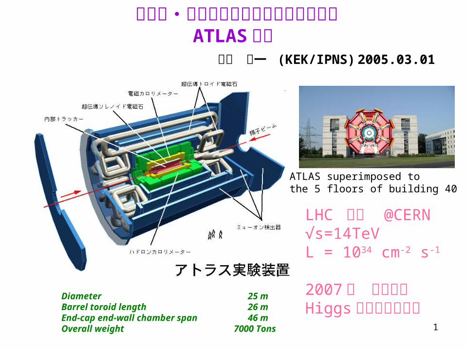
素核研・測定器技術開発の現状とプラン ATLAS 周辺 池上 陽一 (KEK/IPNS)2005.03.01. ATLAS superimposed to the 5 floors of building 40. LHC 計画 @CERN √s=14TeV L = 10 34 cm -2 s -1 2007 年 実験開始 Higgs の発見を焦点に. Diameter25 m Barrel toroid length26 m End-cap end-wall chamber span46 m - PowerPoint PPT PresentationTRANSCRIPT
1
素核研・測定器技術開発の現状とプランATLAS 周辺
池上 陽一 (KEK/IPNS) 2005.03.01
Diameter 25 mBarrel toroid length 26 mEnd-cap end-wall chamber span 46 mOverall weight 7000 Tons
ATLAS superimposed tothe 5 floors of building 40
LHC 計画 @CERN√s=14TeVL = 1034 cm-2 s-1
2007 年 実験開始Higgs の発見を焦点に
2
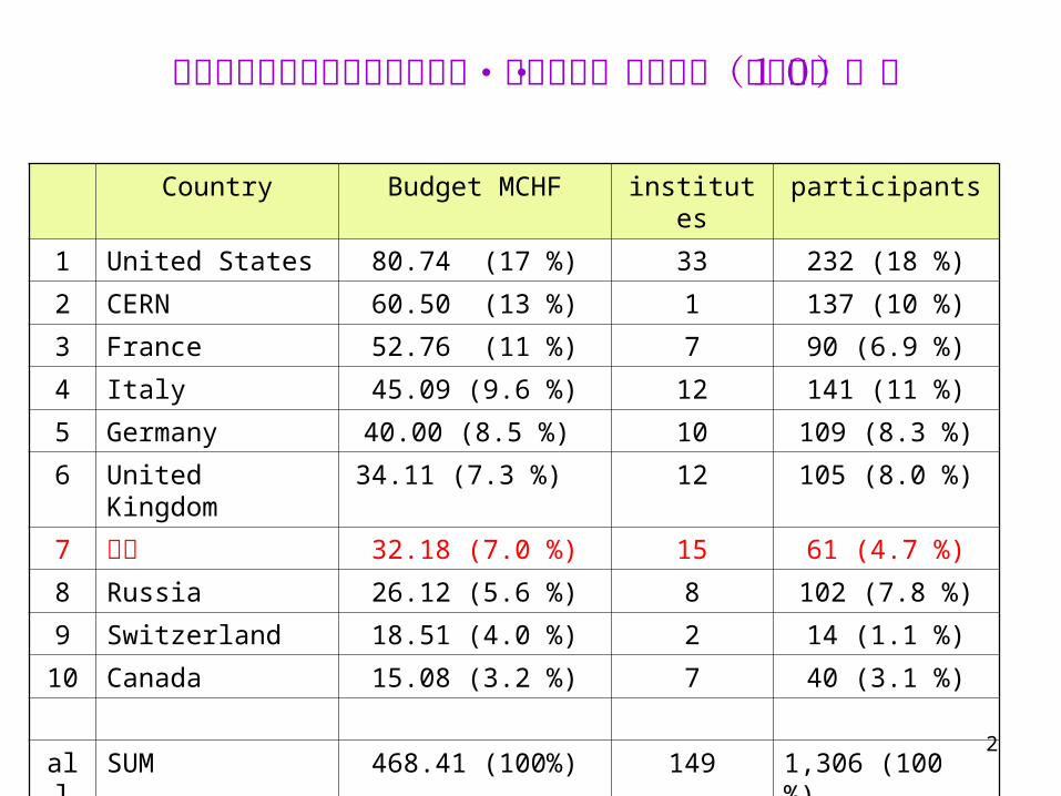
Country Budget MCHF institutes participants
1 United States 80.74 (17 %) 33 232 (18 %)
2 CERN 60.50 (13 %) 1 137 (10 %)
3 France 52.76 (11 %) 7 90 (6.9 %)
4 Italy 45.09 (9.6 %) 12 141 (11 %)
5 Germany 40.00 (8.5 %) 10 109 (8.3 %)
6 United Kingdom 34.11 (7.3 %) 12 105 (8.0 %)
7 日本 32.18 (7.0 %) 15 61 (4.7 %)
8 Russia 26.12 (5.6 %) 8 102 (7.8 %)
9 Switzerland 18.51 (4.0 %) 2 14 (1.1 %)
10 Canada 15.08 (3.2 %) 7 40 (3.1 %)
all SUM 468.41 (100%) 149 1,306 (100 %)
アトラス国際チームの財政分担・参加機関・研究者数(トップ10)
3
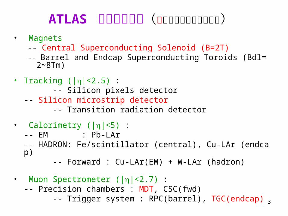
ATLAS 測定器の構成(赤は日本グループが関与)• Magnets
-- Central Superconducting Solenoid (B=2T)-- Barrel and Endcap Superconducting Toroids (Bdl=2~8Tm)
• Tracking (||<2.5) : -- Silicon pixels detector
-- Silicon microstrip detector -- Transition radiation detector
• Calorimetry (||<5) :-- EM : Pb-LAr-- HADRON: Fe/scintillator (central), Cu-LAr (endcap)
-- Forward : Cu-LAr(EM) + W-LAr (hadron)
• Muon Spectrometer (||<2.7) : -- Precision chambers : MDT, CSC(fwd)
-- Trigger system : RPC(barrel), TGC(endcap)
4
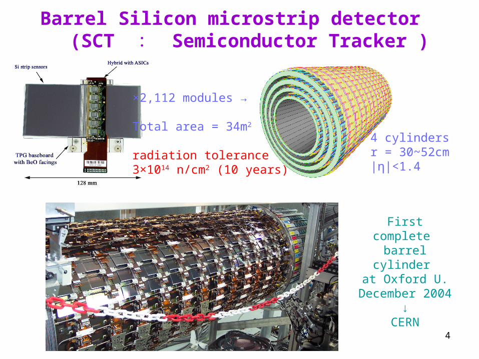
Barrel Silicon microstrip detector (SCT : Semiconductor Tracker )
4 cylindersr = 30~52cm|η|<1.4
×2,112 modules →
Total area = 34m2
radiation tolerance3×1014 n/cm2 (10 years)
First complete barrel cylinder
at Oxford U.December 2004
↓CERN

5
Barrel SCT modules
Specifications:Strip pitch : 80 μmStereo angle : 40 mrreadout channels ; 1536 ch~ 5000 wire bondings Assembly accuracy < 5 μm
Parts: 4 Silicon sensors (Hamamatsu)12 ABCD chips (BiCMOS ASIC)TPG thermal conductor (UK)Flexible hybrid circuit (Japan)
Fablication:Total: 2600 modules980 in Japan (best yield > 95%)Others in UK, US and Scandinavia
6
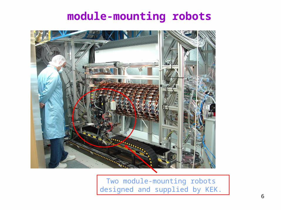
module-mounting robots
Two module-mounting robots designed and supplied by KEK.
7
Barrel SCT における主要な測定器技術開発
• Radiation-hard Si センサーの設計開発• High-density low-mass Readout Hybrid ( COB )の設計開発• 1μm 精度の module の組み立て、及び検査方法の確立• 5K wire bondings x 1K module -> 5M WB sの経験• module-mounting robot の設計開発• Laser による Module 検査方法の確立• IR カメラによる Si センサーの不良解析
8
・電磁カロリメターの内側なので肉厚を極力薄くした:
→ 高強度のアルミニウムを採用(古河・日立電線と技術開発)
→ クライオスタットを液体アルゴンカロリメータと共用
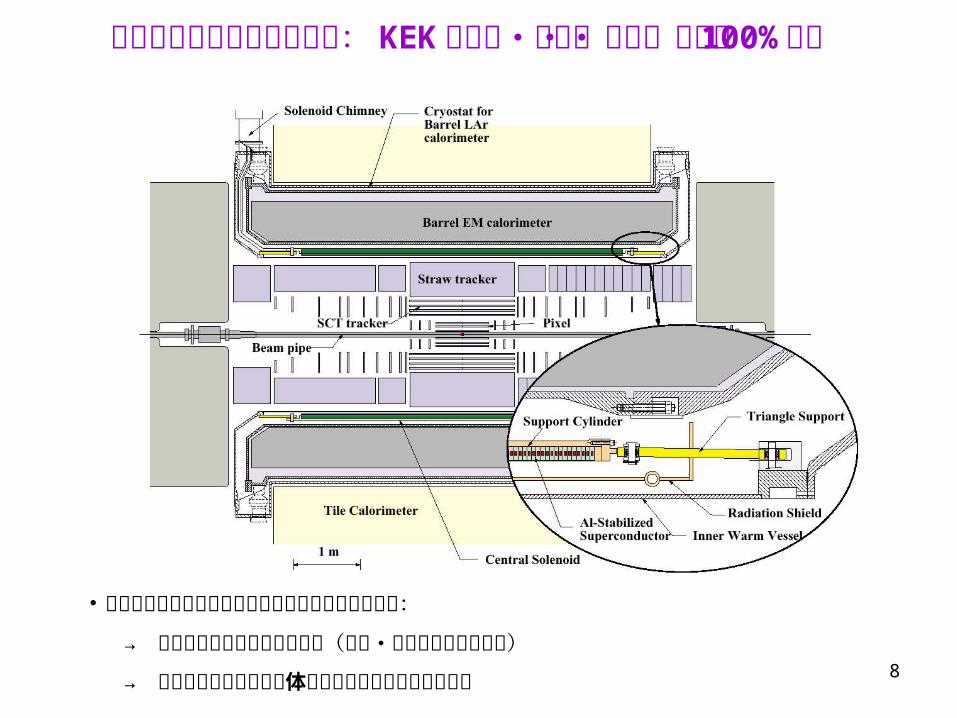
アトラス超伝導ソレノイド: KEK が提案・設計・開発・建設を100% 担当
9
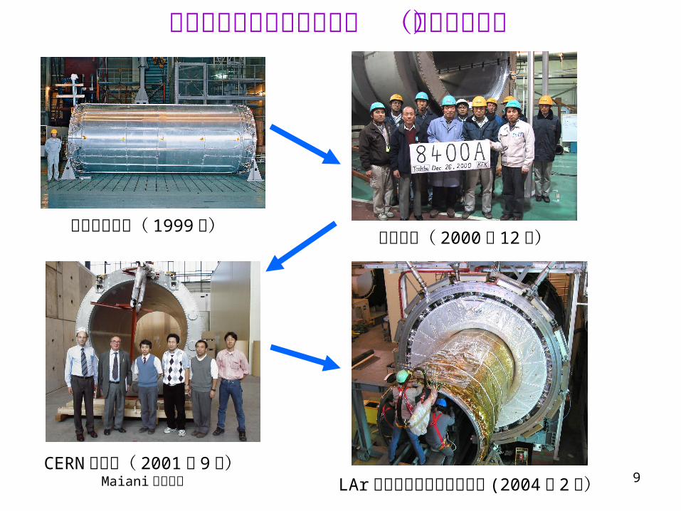
アトラス超伝導ソレノイド (日本が担当)
東芝京浜工場( 1999年) 励磁成功( 2000年 12月)
CERN に到着( 2001 年 9月)
Maiani 所長らとLAr クライオスタットへ据付 (2004 年 2
月)
10
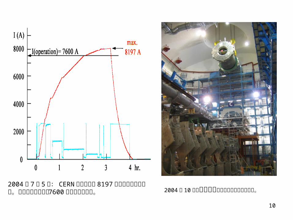
2004 年 7 月 5 日: CERN 地上試験で 8197 アンペアを達成した。通常の運転電流は 7600 アンペアである。
2004 年 10 月にアトラス地下実験場に運搬された。
11
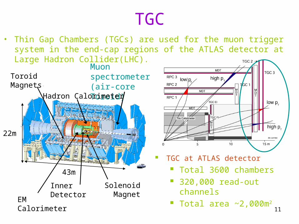
TGC• Thin Gap Chambers (TGCs) are used for the muon trigger system in the
end-cap regions of the ATLAS detector at Large Hadron Collider(LHC).
Muon spectrometer(air-core Toroid)
EM Calorimeter
Hadron Calorimeter
Inner Detector
Toroid Magnets
Solenoid Magnet
22m
43m
TGC at ATLAS detector Total 3600 chambers 320,000 read-out
channels Total area ~2,000m2
12
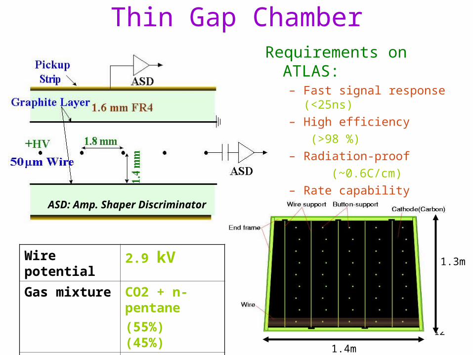
Thin Gap ChamberRequirements on ATLAS:
– Fast signal response (<25ns)
– High efficiency
(>98 %)
– Radiation-proof
(~0.6C/cm)
– Rate capability
(~kHz/cm2)
Wire potential 2.9 kVGas mixture CO2 + n-
pentane
(55%) (45%)
Wire diameter 50 m
ASD: Amp. Shaper Discriminator
1.4m
1.3m
13
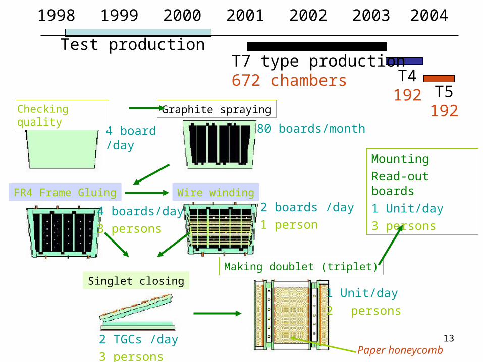
Graphite spraying
FR4 Frame Gluing Wire winding
Singlet closingMaking doublet (triplet)
Paper honeycomb
4 board /day 80 boards/month
4 boards/day3 persons
2 boards /day1 person
2 TGCs /day3 persons
1 Unit/day2 persons
Mounting Read-out boards1 Unit/day3 persons
Checking quality
1998 1999 2000 2001 2002 2003 2004
Test productionT7 type production672 chambers T4
192 T5192

14
TGC chamber Quality Control• TGC is fabricated by the gluing
processes (we can no longer reopen it after closing TGC).
• We have to control the surface distortion less than 200 m
• We apply following tests: Measurement of the surface
resistance of cathode after the graphite spraying,
High voltage test before and after closing singlet TGC,
Pulse test after mounting adapter board and
High voltage test after mounting adapter board.
Pulse response check by -ray radioactive source
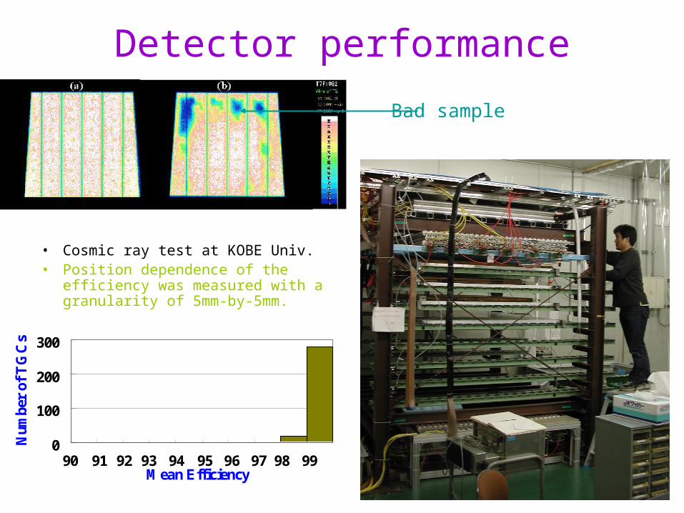
Cosmic ray test at KOBE Univ.
15
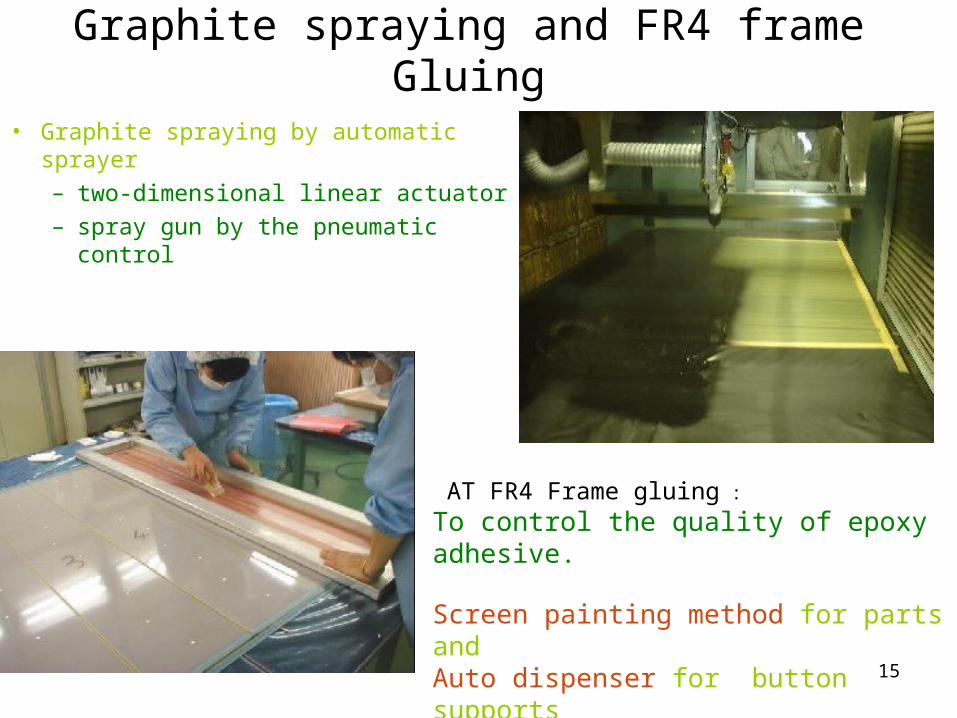
Graphite spraying and FR4 frame Gluing
• Graphite spraying by automatic sprayer– two-dimensional linear actuator – spray gun by the pneumatic control
AT FR4 Frame gluing :
To control the quality of epoxy adhesive. Screen painting method for parts andAuto dispenser for button supportsare adopted.
16
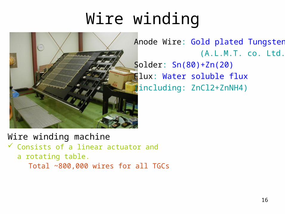
Wire winding
Wire winding machine Consists of a linear actuator and
a rotating table. Total ~800,000 wires for all TGCs
Anode Wire: Gold plated Tungsten (A.L.M.T. co. Ltd.)
Solder: Sn(80)+Zn(20)Flux: Water soluble flux (including: ZnCl2+ZnNH4)
17
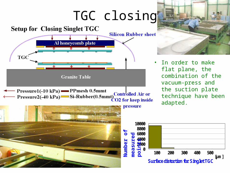
02000400060008000
10000
100 200 300 400 500 [μm]
Surface distortion for Singlet TGC
TGC closing
• In order to make flat plane, the combination of the vacuum-press and the suction plate technique have been adapted.
Nu
mb
er o
f
mea
sure
d p
oin
ts
18
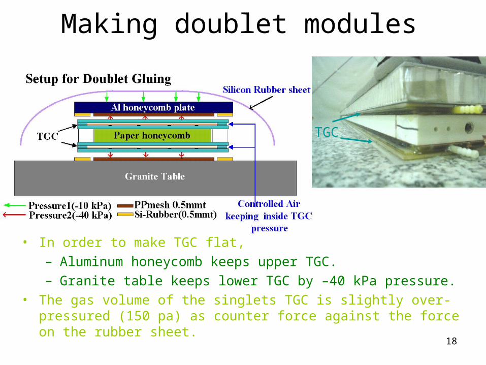
Making doublet modules
• In order to make TGC flat,– Aluminum honeycomb keeps upper TGC.– Granite table keeps lower TGC by –40 kPa pressure.
• The gas volume of the singlets TGC is slightly over-pressured (150 pa) as counter force against the force on the rubber sheet.
TGC
19
0
100
200
300
Mean Efficiency
Num
ber
of T
GC
s
90 91 92 93 94 95 96 97 98 99
Detector performance
• Cosmic ray test at KOBE Univ.• Position dependence of the
efficiency was measured with a granularity of 5mm-by-5mm.
Bad sample
20
TGC chamber Summary
• 1200 TGCs have been produced in Japan – We created the required environment to make
2 TGCs/day.
• We have to make uniform quality– Controlling the TGC’s surface distortion < 200 m
• We have developed some tools
(screen painting method or air control at gluing)
21
Atlas TGC ASICs• 320k channels Muon Trigger Chambers• L1 Trigger and Readout Circuits
– Synchronous (40MHz) track finding circuits (<20 clks latency)
– 100 kHz trigger rate
• On-detector electronics– 耐放射線性 (全ての半導体の照射試験を行う)
• TID:50 krad ( 最大時:安全係数込み)• SEE:2.11x10¹⁰ h/cm2/10 years (安全係数なし)• FPGA が使用出来ない
– 許容消費電力、スペースの制限– チャンネル単価 : 目標 \1,000/ch (全エレキシス
テムで)• 4 種類の ASIC の開発
– Atlas TGC 日本グループと KEK 回路室– ASD, Patch-Panel ASIC, SLB ASIC, H-pT ASIC
22
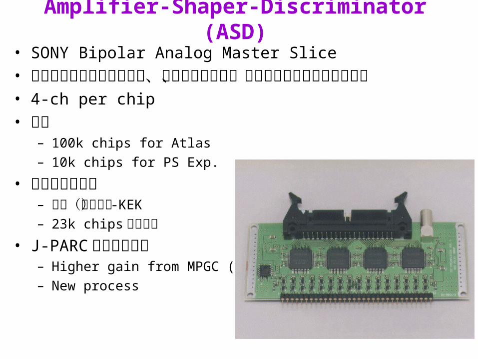
Amplifier-Shaper-Discriminator (ASD)
• SONY Bipolar Analog Master Slice• 回路設計全てを自前で行い、配線レイアウト、プロセスの
みをソニーに委託• 4-ch per chip• 量産
– 100k chips for Atlas– 10k chips for PS Exp.
• 積分時間変更版– 京大(谷森研) -KEK– 23k chips 共同購入
• J-PARC 等からの要請– Higher gain from MPGC (JAERI)– New process
23
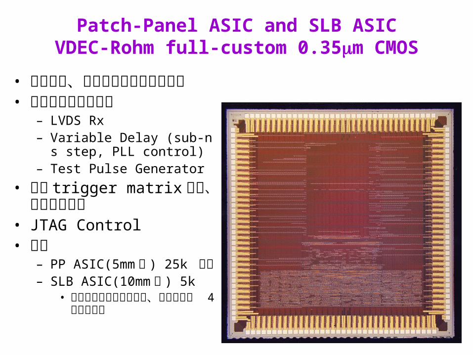
Patch-Panel ASIC and SLB ASICVDEC-Rohm full-custom 0.35m CMOS
• 回路設計、レイアウト設計全て自前
• アナログ回路の設計– LVDS Rx– Variable Delay (sub-ns step,
PLL control)– Test Pulse Generator
• 初段 trigger matrix 回路 読、み出し回路
• JTAG Control • 量産
– PP ASIC(5mm 角 ) 25k 済み
– SLB ASIC(10mm 角 ) 5k • 度重なる失敗を繰り返し、
ついに完成 4 月量産予定

24
H-pT ASICVDEC-Hitachi 0.35m CMOS Gate Array
• 回路設計、レイアウト設計全て自前• 第 2 段 trigger matrix (all logic)• FPGA 感覚で出来た!
– でも、後からバグが見つかったりする。外付け回路で逃げる。• 1.2k chips 量産
• FPGA では無理?– 放射線 SEE
– 多入出力– 多配線資源– 多 Flip-Flop
– FPGA 自動配置 配線では辛い
25
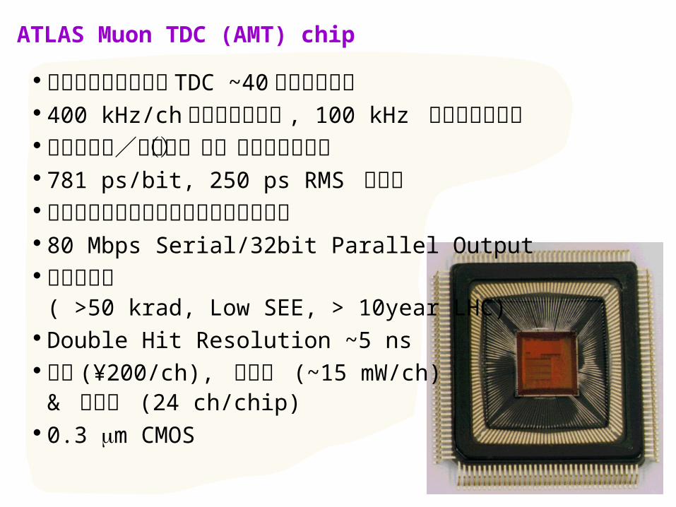
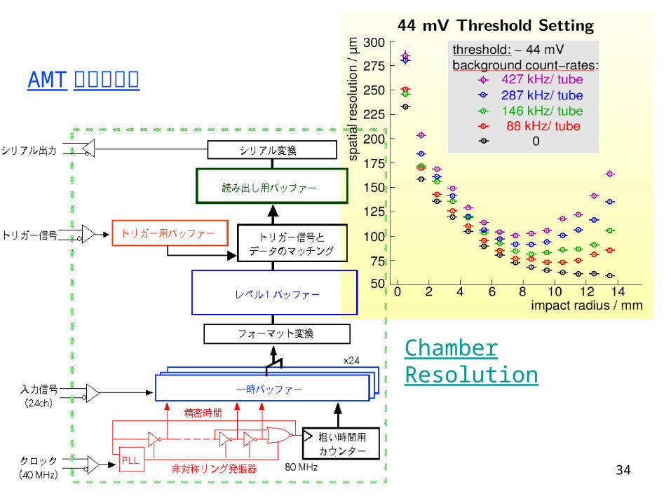
ATLAS Muon TDC (AMT) chip
ミューオン検出器用 TDC ~40 万チャンネル 400 kHz/ch 最大入力レート , 100 kHz トリガーレート 立ち上がり/下がり(幅)エッジ時間測定 781 ps/bit, 250 ps RMS 分解能 トリガーに対応したデータのみ選択出力 80 Mbps Serial/32bit Parallel Output 放射線耐性
( >50 krad, Low SEE, > 10year LHC) Double Hit Resolution ~5 ns 安価 (¥200/ch), 低電力 (~15 mW/ch) & 高密度 (24 ch/chip)
0.3 m CMOS
26
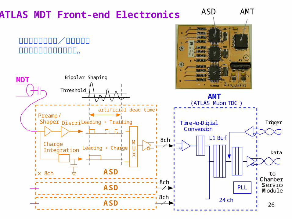
MDT
Preamp/Shaper Discri
Charge Integration
Trigger
24 ch
x 8 ch ASD
AMT (ATLAS Muon TDC)
MUX
8ch
Data
8ch
ASD
ASD
Leading + Trailing
Threshold
Leading + Charge
8ch
artificial dead time
Bipolar Shaping
Time-to-Digital Conversion
PLL
L1 Buf
to Chamber Service Module
ATLAS MDT Front-end Electronics
信号の立ち上がり/下がり及びスルーレートの測定を行う。
ASD AMT
27
• 20,000 チップ量産終了。
• 17,000 Frontend Board 生産終了。
• 現在チェンバーへの取付中。
ATLAS AMT 現状
• AMT-VME ボード (~100 台販売 ), K2K, Cangaroo, 理研…
• Bell アップグレード (Copper TDC Finess ボード )
• Bepi Colimbo 水星探査衛星 ( 宇宙科学研)搭載予定。
• Super-K アップグレード(〜4万チャンネル ) 使用予定。
• Ionwerks Inc. 微量分析装置(米国)
他実験での応用
28
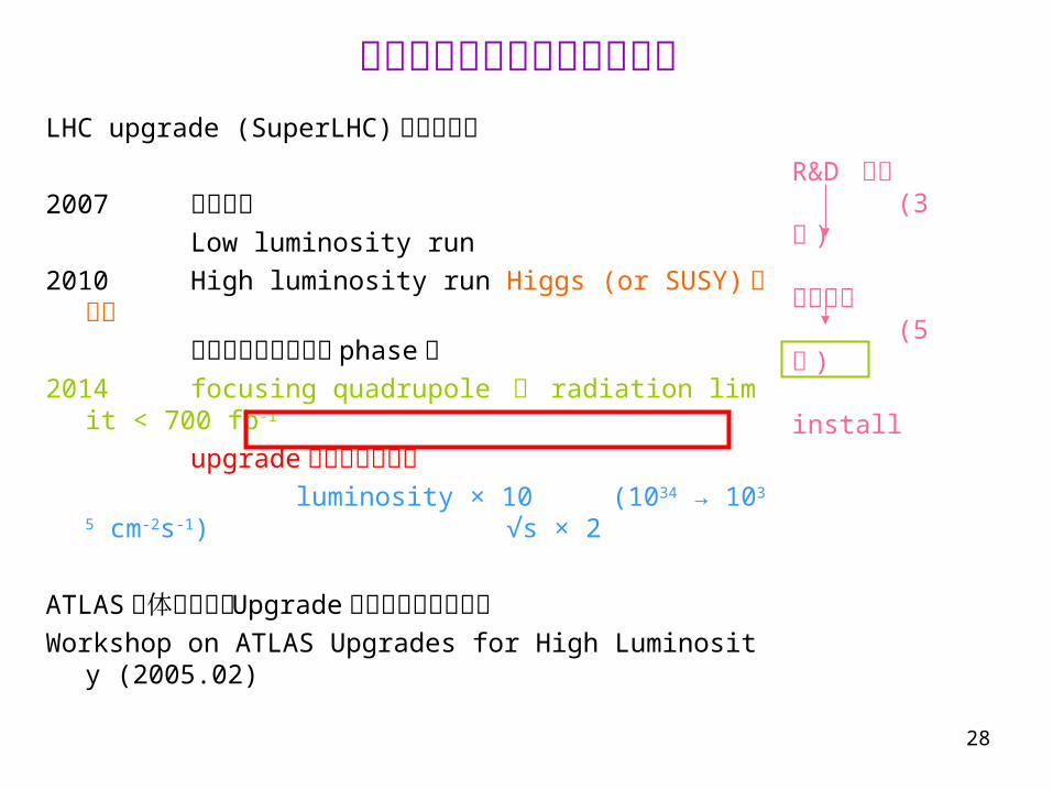
次期測定器技術開発のプラン
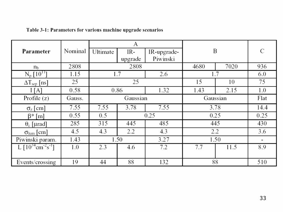
LHC upgrade (SuperLHC) のシナリオ
2007 実験開始 Low luminosity run
2010 High luminosity run Higgs (or SUSY) 発見か
発見から精密測定の phase へ 2014 focusing quadrupole の radiation limit < 700 fb-1
upgrade の可能性を検討luminosity × 10 (1034 → 1035 cm-2s-1)
√s × 2
ATLAS 全体としても Upgrade の詳細な検討が開始Workshop on ATLAS Upgrades for High Luminosity (2005.02)
R&D 開始(3
年 )
量産開始(5
年 )
install
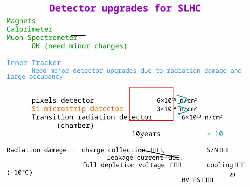
29
Detector upgrades for SLHCMagnetsCalorimeterMuon Spectrometer
OK (need minor changes)
Inner Tracker Need major detector upgrades due to radiation damage and large occupancy
pixels detector 6×10¹⁵ n/cm2
Si microstrip detector 3×10¹⁴ n/cm2
Transition radiation detector 6×10¹³ n/cm2
(chamber)10years × 10
Radiation damege → charge collection の悪化、 S/N の悪化 leakage current の増大、
full depletion voltage の増大 cooling の負担 (-10 )℃
HV PS の負担
30
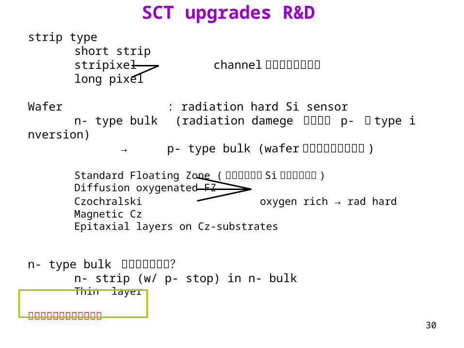
SCT upgrades R&Dstrip type
short stripstripixel channel 数を押さえる工夫long pixel
Wafer : radiation hard Si sensorn- type bulk (radiation damege を受けて p- に type inversion)
→ p- type bulk (wafer の安定な入手が困難 )
Standard Floating Zone ( 高抵抗単結晶 Si の製法の標準 )Diffusion oxygenated FZCzochralski oxygen rich → rad hardMagnetic Cz Epitaxial layers on Cz-substrates
n- type bulk は使えないのか?n- strip (w/ p- stop) in n- bulkThin layer
量産可能な技術であること
31
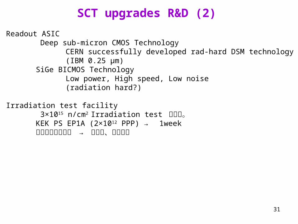
SCT upgrades R&D (2)
Readout ASIC Deep sub-micron CMOS Technology
CERN successfully developed rad-hard DSM technology (IBM 0.25 μm)
SiGe BICMOS TechnologyLow power, High speed, Low noise(radiation hard?)
Irradiation test facility 3×10¹⁵ n/cm2 Irradiation test が必要。KEK PS EP1A (2×10¹² PPP) → 1week放射化物質の移動 → 国内で、行いたい
32
資料
33
34
AMT ブロック図
Chamber Resolution
35
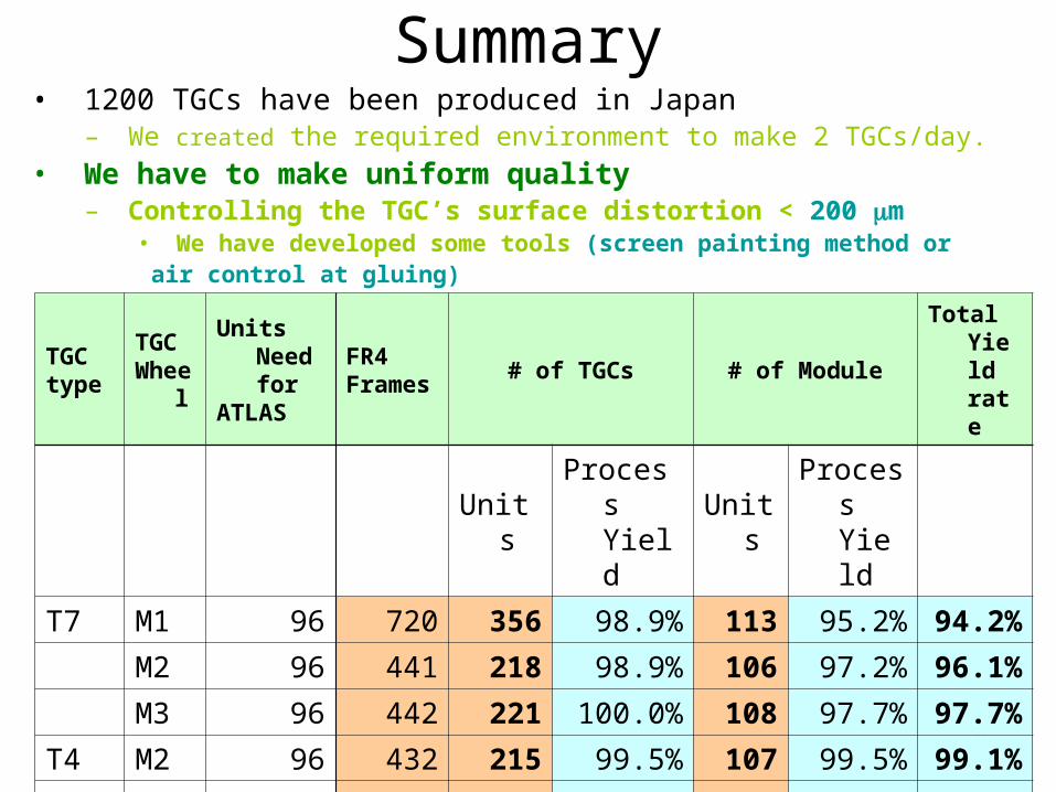
Summary• 1200 TGCs have been produced in Japan
– We created the required environment to make 2 TGCs/day.
• We have to make uniform quality– Controlling the TGC’s surface distortion < 200 m
• We have developed some tools (screen painting method or air control at gluing)
TGC type
TGCWhe
el
Units Need for
ATLAS
FR4Frame
s# of TGCs # of Module
Total Yield rate
UnitsProcess
YieldUnit
s
Process Yield
T7 M1 96 720 356 98.9% 113 95.2%94.2
%
M2 96 441 218 98.9% 106 97.2%96.1
%
M3 96 442 221 100.0% 108 97.7%97.7
%
T4 M2 96 432 215 99.5% 107 99.5%99.1
%
T5 M3 96 433 214 98.8% 107100.0
%98.8
%
SUM 480 2468 1224 541