博士論文 doctoral dissertation development and study of pp · pdf file博士論文...
TRANSCRIPT
博 士 論 文Doctoral Dissertation
Development and Study of the Level-1 Trigger System for the
ATLAS Experiment at the Large Hadron Collider
(LHC 加速器における ATLAS 実験用 Level-1 トリガシステムの開発及びその研究)
Ryo Ichimiya
February, 2006
Graduate School ofScience and Technology
Kobe University

Abstract
The main objectives of the ATLAS Experiment at the Large Hadron Collider are to search for
the Higgs boson(s), to verify the Standard Model, to measure Standard Model parameters more
precisely and to explore the physics beyond the Standard Model in higher energy range of up to
a few TeV. This experiment has to handle tremendous data flow, far more than any experiment
have done ever. Therefore extremely powerful trigger system to reduce the event rate efficiently
is essential. The ATLAS Trigger system consists of three trigger stages: Level-1 Trigger, Level-
2 Trigger and Event Filter. In order to extract interesting physics results efficiently from high
luminosity proton-proton interactions in high radiation environment, special architecture and
devices are required in the Level-1 Trigger and data acquisition system (TDAQ).
The author developed two key devices for the TDAQ of the ATLAS Endcap muon Trigger
system which use detectors called Thin Gap Chamber (TGC). This Trigger system was designed
through a physics performance study with Monte Carlo simulation. Furthermore a trigger
logic simulator has developed to check the correctness trigger logic system. Due to the space
availability and timing consideration, the TGC front-end electronics will be placed on the TGC
surface where the radiation level is high (∼210 Gy for ten years). The high radiation level causes
not only damage to the devices but also limitation of access for maintenance. This situation
made the design work for the trigger electronics much more difficult.
We chose and developed Application Specific Integrated Circuit (ASIC) for the front-end
core part of the TDAQ. The ASICs are manufactured using the latest technology to have
inherently higher radiation tolerance level. It also has favorable characteristics of high-speed
data processing, low power consumption, low cost (in mass production) and small area. A
lot of efforts were made to develop the ASIC with high enough performance for the ATLAS
Experiment.
The Endcap muon Trigger system has flexibility in setting threshold of transverse momen-
tum level to classify incoming muons. This part of function is done at the Sector Logic, the
final part of the Endcap muon Trigger system located in electronics hut. We chose to use the
latest Field Programmable Gate Array (FPGA) for the Sector Logic. The Sector Logic needs
to operate with low latency and needs to have flexibility in setting different threshold level.
The author developed the algorithm and made the final prototype of the Sector Logic.
In order to confirm the radiation tolerance of the semiconductor devices used in the Endcap
muon Trigger electronics system, we have executed γ-ray and proton beam irradiation tests for
these devices.
The ATLAS TDAQ system has been developed and constructed. The ATLAS Experiment
is scheduled to start taking data in 2007.

Acknowledgement
I would like to thank my supervisor Prof. Hiroshi Takeda and Prof. Hisaya Kurashige for their
support and guidance over the entire years. I also give my special thanks to Prof. Osamu Sasaki
who continuously gave me valuable guidance and support. I would like to express special thanks
to Mr. Masahiro Ikeno for technical suggestion and support at the electronics development. I
would also like to address special thanks to Prof. Yasuo Arai for technical/theoretical suggestion
and support in the development of the ASICs and in the semiconductor irradiation tests. I
would like to express thanks to Dr. Hiroyuki Kano for technical support and advice in the ASIC
development. I’m very grateful to Dr. Kentaro Mizouchi for co-works in the ASIC development
and various discussions with me. I would like to thank to Mr. Takeshi Ogata for co-works
for the Sector Logic development. I also would like to express special thanks to Mrs. Yumi
Yokoyama for various support of our studies at our laboratory.
I would like to thank to Prof. Takahiko Kondo, Prof. Chikara Fukunaga, Prof. Hiroshi
Sakamoto, Dr. Masaya Ishino, Prof. Mitsuaki Nozaki, Prof. Kiyotomo Kawagoe, Dr. Atsuhiko
Ochi, Dr. Kazumi Hasuko, Prof. Tokio Kenneth Ohska, Prof. Hiroyuki Iwasaki and Prof. Tomio
Kobayashi for their support and advice.
I would like to give special thanks to Prof. Tohru Takeshita for giving a chance to enter
this exciting world of experimental particle physics studies.
I would like to thank all colleagues at Kobe University, at the ATLAS TGC Electronics
Group and at the ATLAS collaboration.
Finally, I would like to thank my parents and family for their continuous and tremendous
support plus encouragement until now.
1

Contents
0 Introduction 9
1 The ATLAS Experiment 12
1.1 The Large Hadron Collider . . . . . . . . . . . . . . . . . . . . . . . . . . . . . 12
1.1.1 The LHC Accelerator Complex . . . . . . . . . . . . . . . . . . . . . . . 12
1.1.2 The Bending (Dipole) Magnets in the LHC . . . . . . . . . . . . . . . . 14
1.2 Physics at the ATLAS Experiment . . . . . . . . . . . . . . . . . . . . . . . . . 15
1.2.1 The Standard Model . . . . . . . . . . . . . . . . . . . . . . . . . . . . . 15
1.2.2 Physics Potential . . . . . . . . . . . . . . . . . . . . . . . . . . . . . . . 16
1.2.3 Higgs Boson . . . . . . . . . . . . . . . . . . . . . . . . . . . . . . . . . . 17
1.3 The ATLAS Detector . . . . . . . . . . . . . . . . . . . . . . . . . . . . . . . . 19
1.3.1 Overview . . . . . . . . . . . . . . . . . . . . . . . . . . . . . . . . . . . 19
1.3.2 Inner Detector . . . . . . . . . . . . . . . . . . . . . . . . . . . . . . . . 20
1.3.3 Calorimetry . . . . . . . . . . . . . . . . . . . . . . . . . . . . . . . . . . 20
1.3.3.1 Electromagnetic Calorimeter . . . . . . . . . . . . . . . . . . . 21
1.3.3.2 Hadronic Calorimeter . . . . . . . . . . . . . . . . . . . . . . . 21
1.3.4 Muon Spectrometer . . . . . . . . . . . . . . . . . . . . . . . . . . . . . 23
1.3.4.1 Monitored Drift Tube (MDT) . . . . . . . . . . . . . . . . . . 24
1.3.4.2 Cathode Strip Chamber (CSC) . . . . . . . . . . . . . . . . . . 24
1.3.4.3 Resistive Plate Chamber (PRC) . . . . . . . . . . . . . . . . . 25
1.3.4.4 Thin Gap Chamber (TGC) . . . . . . . . . . . . . . . . . . . . 26
2 The ATLAS Trigger/Data-Acquisition (TDAQ) System 28
2.1 Level-1 (LVL1) Trigger Overview . . . . . . . . . . . . . . . . . . . . . . . . . . 30
2.1.1 Muon Trigger . . . . . . . . . . . . . . . . . . . . . . . . . . . . . . . . . 31
2.2 Timing, Trigger and Control (TTC) distribution system . . . . . . . . . . . . . 32
3 The Endcap Muon (TGC) Trigger System 33
3.1 Layout and its Algorithm . . . . . . . . . . . . . . . . . . . . . . . . . . . . . . 33
3.2 Implementation on the Electronics System . . . . . . . . . . . . . . . . . . . . . 34
3.3 Trigger Sector . . . . . . . . . . . . . . . . . . . . . . . . . . . . . . . . . . . . . 36
2

3.4 Latency . . . . . . . . . . . . . . . . . . . . . . . . . . . . . . . . . . . . . . . . 38
4 System Development Issues 40
4.1 Technology selections for the system components . . . . . . . . . . . . . . . . . 40
4.2 Slave Board ASIC . . . . . . . . . . . . . . . . . . . . . . . . . . . . . . . . . . 43
4.2.1 Overview . . . . . . . . . . . . . . . . . . . . . . . . . . . . . . . . . . . 43
4.2.2 Master-Slave Structure . . . . . . . . . . . . . . . . . . . . . . . . . . . . 44
4.2.3 Block Diagram . . . . . . . . . . . . . . . . . . . . . . . . . . . . . . . . 44
4.2.4 Input Block . . . . . . . . . . . . . . . . . . . . . . . . . . . . . . . . . . 45
4.2.5 Low-pT trigger Block . . . . . . . . . . . . . . . . . . . . . . . . . . . . 46
4.2.5.1 Coincidence Matrix for Doublets pair (DSB) . . . . . . . . . . 47
4.2.5.2 Triplet Slave Board (TSB) . . . . . . . . . . . . . . . . . . . . 50
4.2.5.3 EI/FI Slave Board (EFSB) . . . . . . . . . . . . . . . . . . . . 53
4.2.6 Readout Block . . . . . . . . . . . . . . . . . . . . . . . . . . . . . . . . 55
4.2.7 JTAG Block . . . . . . . . . . . . . . . . . . . . . . . . . . . . . . . . . 56
4.2.8 Implementation on the ASIC . . . . . . . . . . . . . . . . . . . . . . . . 58
4.2.9 Validation . . . . . . . . . . . . . . . . . . . . . . . . . . . . . . . . . . . 58
4.3 Sector Logic . . . . . . . . . . . . . . . . . . . . . . . . . . . . . . . . . . . . . . 61
4.3.1 Overview . . . . . . . . . . . . . . . . . . . . . . . . . . . . . . . . . . . 61
4.3.2 Design of the Sector Logic . . . . . . . . . . . . . . . . . . . . . . . . . . 61
4.3.2.1 R-φ coincidence . . . . . . . . . . . . . . . . . . . . . . . . . . 62
4.3.2.2 Track Selection Logic (Pre-Track Selector, Track Selector) . . 63
4.3.2.3 Decoder . . . . . . . . . . . . . . . . . . . . . . . . . . . . . . . 63
4.3.2.4 Encoder . . . . . . . . . . . . . . . . . . . . . . . . . . . . . . . 69
4.3.3 The first prototype (Prototype-0) . . . . . . . . . . . . . . . . . . . . . . 72
4.3.3.1 Specification . . . . . . . . . . . . . . . . . . . . . . . . . . . . 72
4.3.3.2 Implementaion . . . . . . . . . . . . . . . . . . . . . . . . . . . 73
4.3.3.3 Validation . . . . . . . . . . . . . . . . . . . . . . . . . . . . . 74
4.3.3.4 Integration test with the MUCTPI . . . . . . . . . . . . . . . . 74
4.3.3.5 Test beam at H8 beam line in CERN . . . . . . . . . . . . . . 74
4.3.4 Final Design of whole Sector Logic system . . . . . . . . . . . . . . . . . 75
4.3.4.1 Final Design of Sector Logic board . . . . . . . . . . . . . . . . 77
4.4 Radiation Tolerance . . . . . . . . . . . . . . . . . . . . . . . . . . . . . . . . . 80
4.4.1 Test for Total Ionization Dose (TID) . . . . . . . . . . . . . . . . . . . . 80
4.4.1.1 TID Test Procedure . . . . . . . . . . . . . . . . . . . . . . . . 80
4.4.1.2 Results of the TID tests . . . . . . . . . . . . . . . . . . . . . . 81
4.4.2 Test for Single Event Effect (SEE) . . . . . . . . . . . . . . . . . . . . . 86
4.4.2.1 SEE Test Procedure . . . . . . . . . . . . . . . . . . . . . . . . 87
3
4.4.2.2 SEE cross sections for individual chips . . . . . . . . . . . . . . 88
4.4.3 Summary of the irradiation tests . . . . . . . . . . . . . . . . . . . . . . 89
5 Summary and Conclusions 90
Reference 92
4
List of Figures
1.1 LHC and Injection Complex at CERN. . . . . . . . . . . . . . . . . . . . . . . . 13
1.2 Schematic layout of the LHC. Beam 1 circulates clockwise and Beam 2 Counter-
Clockwise. . . . . . . . . . . . . . . . . . . . . . . . . . . . . . . . . . . . . . . . 13
1.3 Cross Section of LHC Tunnel with showing the LHC machine cross section. . . 15
1.4 Feynman-Diagrams for Higgs Boson Production. . . . . . . . . . . . . . . . . . 18
1.5 Decay branching fraction of StandardModelHiggs. . . . . . . . . . . . . . . . . 18
1.6 The ATLAS detector overview. . . . . . . . . . . . . . . . . . . . . . . . . . . . 20
1.7 Inner Detector. . . . . . . . . . . . . . . . . . . . . . . . . . . . . . . . . . . . . 21
1.8 Layout of the Calorimeters. . . . . . . . . . . . . . . . . . . . . . . . . . . . . . 22
1.9 Total thickness (in radiation length) of the ATLAS EM calorimeter as a function
of η. . . . . . . . . . . . . . . . . . . . . . . . . . . . . . . . . . . . . . . . . . . 22
1.10 Amount of material (absorption length) in the ATLAS Calorimetry as a function
of η. . . . . . . . . . . . . . . . . . . . . . . . . . . . . . . . . . . . . . . . . . . 22
1.11 R-Z View of the ATLAS Muon Spectrometer. . . . . . . . . . . . . . . . . . . . 24
1.12 The MDT (Monitored Drift Tube). . . . . . . . . . . . . . . . . . . . . . . . . . 24
1.13 The CSC (Cathode Strip Tube). . . . . . . . . . . . . . . . . . . . . . . . . . . 25
1.14 The RPC (Resistive Plate Chamber). . . . . . . . . . . . . . . . . . . . . . . . . 25
1.15 TGC structure showing anode wires, graphite cathodes, G-10 layers, and read-
out strip orthogonal to the wires. . . . . . . . . . . . . . . . . . . . . . . . . . . 26
1.16 Cross-section of a triplet (left) and of a doublet of TGCs (right). . . . . . . . . 27
2.1 Schematic diagram of the ATLAS Trigger and DAQ System. . . . . . . . . . . 29
2.2 ATLAS LVL1 Trigger System. . . . . . . . . . . . . . . . . . . . . . . . . . . . . 30
2.3 Layout of the ATLAS Muon Trigger Chambers. . . . . . . . . . . . . . . . . . . 31
3.1 The Longitudinal view of the TGC system. . . . . . . . . . . . . . . . . . . . . 33
3.2 Overview of the TGC LVL1 Trigger electronics system. . . . . . . . . . . . . . 35
3.3 TGC electronics placement. . . . . . . . . . . . . . . . . . . . . . . . . . . . . . 37
5
3.4 TGC LVL1 Trigger segmentation for an octant (one eights of pivot plane). One
octant wheel is divided into six ENDCAP sectors and three FORWARD sectors.
Bold lines in the figure indicate individual trigger sectors. They are further
subdivided into trigger subsectors. . . . . . . . . . . . . . . . . . . . . . . . . . 38
3.5 Wire-signal segmentation. Each small box represents a segment of 32 channels,
corresponding to 4 subsectors. . . . . . . . . . . . . . . . . . . . . . . . . . . . . 39
4.1 Voting Logic implementation: Three D-type FlipFlops are used to implement
1bit Voting Register. Even if any one register value flipped, the data out keeps
the initial value. . . . . . . . . . . . . . . . . . . . . . . . . . . . . . . . . . . . 41
4.2 Device selection at the TGC electronics system. . . . . . . . . . . . . . . . . . . 42
4.3 Layout Mask pattern of SLB ASIC Version 6. This version is final design and
mass-production has done with this design. . . . . . . . . . . . . . . . . . . . . 43
4.4 Normal Shift Register. . . . . . . . . . . . . . . . . . . . . . . . . . . . . . . . . 44
4.5 Master-Slave Shift Register. . . . . . . . . . . . . . . . . . . . . . . . . . . . . . 44
4.6 Block Diagram of the SLB ASIC. . . . . . . . . . . . . . . . . . . . . . . . . . . 45
4.7 Double mask scheme implemented in the SLB ASIC, two masks are shown in
the (red) solid squares. One is common for the Readout and the Matrix, and
the other one is only for the trigger matrix. . . . . . . . . . . . . . . . . . . . . 46
4.8 Schematic of Delay Circuit of SLB ASIC Input block. At first, the input signal
is latched either on Positive edge (D-FF) or Negative edge (DN-FF). Following
delay shift register circuit is formed by the Master-Slave structure. . . . . . . . 46
4.9 The functional structure of a Slave Board for the TGC doublet pairs. Shown is
the wire Slave Board; the strip Slave Board has 16-bit output instead. . . . . . 47
4.10 Structure of a 3-out-of-4 Doublet Slave Board Low-pT matrix and the encoded
output information. The wire (r) Slave Board is shown. The strip Doublet Slave
Board is similar, but with ∆φ = ±3. . . . . . . . . . . . . . . . . . . . . . . . . 48
4.11 Detailed structure of the 3-out-of-4 Low-pT matrix for wires. Also shown is the
function of a matrix element. Cells with the same shading have the same ∆r.
The matrix for φ is the same, except ∆φ goes from -3 to +3. (Actually X and
Y in the figure are the same.) . . . . . . . . . . . . . . . . . . . . . . . . . . . . 49
4.12 Declustering rules. When a hit pattern wider than two is found, the rules shown
assign a position to the track. . . . . . . . . . . . . . . . . . . . . . . . . . . . . 50
4.13 Slave Board for TGC Triplets (for wire signals). . . . . . . . . . . . . . . . . . . 51
4.14 Structure of the Triplet logic for wire signals. Logic to deal with the staggering
of triplet layers and the output format after encoding is also shown. . . . . . . 51
6

4.15 Functional structure of a Slave Board for TGC Triplet strip signals. There are
only two active layers of strips per “triplet”. One chip handles up to two triplet
units independently. . . . . . . . . . . . . . . . . . . . . . . . . . . . . . . . . . 52
4.16 The functional structure of the triplet Slave Board for strip signals. Logic to
deal with the staggering of triplet layers and output format after the encoder
section is also shown. . . . . . . . . . . . . . . . . . . . . . . . . . . . . . . . . . 53
4.17 Slave Board for the EI/FI TGC doublet. . . . . . . . . . . . . . . . . . . . . . . 54
4.18 The functional structure of the EI/FI Slave Board. Logic to deal with the
staggering of doublet layers and output format after the encoder section is also
shown. . . . . . . . . . . . . . . . . . . . . . . . . . . . . . . . . . . . . . . . . . 54
4.19 Block Diagram of the SLB Readout Block. . . . . . . . . . . . . . . . . . . . . . 55
4.20 Layout of the Readout macro-core. In this figure, alligned rectangles means the
location of the memory macro cells. . . . . . . . . . . . . . . . . . . . . . . . . 56
4.21 A Schematic View of SLB ASIC Test Setup. . . . . . . . . . . . . . . . . . . . . 59
4.22 Various SLB Test Vectors and Results. . . . . . . . . . . . . . . . . . . . . . . . 60
4.23 Block Diagram of Sector Logic (trigger logic functional view). . . . . . . . . . . 62
4.24 Detail of Sub Sector Cluster (SSC) for the R-φ coincidence togher with hit inputs. 63
4.25 A schematic of Track Selection logic block. . . . . . . . . . . . . . . . . . . . . 64
4.26 Data Format from Hi-pT ASIC chip (Wire mode). . . . . . . . . . . . . . . . . 64
4.27 Wire High-pT Boards coverage and its correspondant SSCs. . . . . . . . . . . . 65
4.28 Wire (R) input signal from from Wire High-pT Board. . . . . . . . . . . . . . . 66
4.29 Strip (φ) input signal from from Strip High-pT Board. . . . . . . . . . . . . . . 67
4.30 A Photograph of TGC Sector Logic Prototype-0 (top view). . . . . . . . . . . . 72
4.31 Block Diagram of Sector Logic Prototype-0 (FORWARD Region type). . . . . . 73
4.32 Correlation plots of pT levels (left) and ROI location(right) for trigger words
read out by Sector Logic vs MUCTPI. . . . . . . . . . . . . . . . . . . . . . . . 75
4.33 The Sector Logic system. . . . . . . . . . . . . . . . . . . . . . . . . . . . . . . 76
4.34 The layout of TGC FORWARD Sector Logic (top view). . . . . . . . . . . . . . 79
4.35 The layout of TGC ENDCAP Sector Logic (top view). . . . . . . . . . . . . . . 79
4.36 γ-ray irradiation test setup. . . . . . . . . . . . . . . . . . . . . . . . . . . . . . 81
4.37 VCON voltages of PP ASIC for γ-ray irradiation. . . . . . . . . . . . . . . . . . 82
4.38 Frequencies of Ring Oscillator on Rohm 0.35 µm for γ-ray irradiation. . . . . . 82
4.39 Consumption current of A54SX32A for γ-ray irradiation. . . . . . . . . . . . . 84
4.40 Frequencies of Ring Oscillator on A54SX32A for γ-ray irradiation. . . . . . . . 84
4.41 Consumption current of AX250 for γ-ray irradiation. (1 krad = 10 Gy) . . . . 85
4.42 Frequencies of Ring Oscillator on AX250 for γ-ray irradiation. (1 krad = 10 Gy) 85
4.43 Schematic of proton beam test setup. . . . . . . . . . . . . . . . . . . . . . . . . 87
4.44 Picture of proton beam test setup. . . . . . . . . . . . . . . . . . . . . . . . . . 88
7

List of Tables
1.1 Parameters of the LHC. . . . . . . . . . . . . . . . . . . . . . . . . . . . . . . . 14
1.2 Main Parameters of the dipole magnet. . . . . . . . . . . . . . . . . . . . . . . . 14
1.3 Fundamental Forces and their Bosons. . . . . . . . . . . . . . . . . . . . . . . . 16
3.1 contributions to the total estimated TGC latency, in bunch-crossing in number
of bunch crossing. (BC) (1 BC = 25 ns) . . . . . . . . . . . . . . . . . . . . . . 39
4.1 Control Registers in SLB ASIC. . . . . . . . . . . . . . . . . . . . . . . . . . . . 57
4.2 Data format between Sector Logic and MUCTPI [16]. . . . . . . . . . . . . . . 70
4.3 Compilation of the SEE test results. . . . . . . . . . . . . . . . . . . . . . . . . 89
8

Chapter 0
Introduction
The Standard Model (SM) is a very successful model in describing interactions of the matter
components, applicable to very small scale and high energies. Past experiments, performed
with the Large Electron Positron collider (LEP), have confirmed the validity of the SM up
to the energy of about 200 GeV. However, there still are questions to be answered in the
SM framework such as the existence of the Higgs boson. The next generation collider, where
protons are chosen as the beam particles, is now being built in the LEP tunnel at CERN. Since
the synchrotron radiation is not a serious problem for proton beams at this energy level, the
collider, named as “the Large Hadron Collider” (LHC), can accelerate the beams up to 7 TeV.
The collider offers a large range of physics opportunities and provides the potential to make
tests of the model with the highest energy and to search for signature of physics beyond the
Standard Model.
Since most of the physics questions involve interactions that has very low cross section, not
only the high energy but also the highest possible luminosity is required. The LHC will reach
a luminosity of 1034 cm−2s−1, with inter-bunch crossing time of 25 ns and more than ∼ 109
interactions per second are expected.
ATLAS Experiment is one of the general purpose experiments scheduled to start taking
data at the LHC in 2007. A lot of work is currently underway to complete the ATLAS detector
system. In addition, detailed simulation works are performed in order to estimate the sensitivity
of the ATLAS Experiment to various interesting physics processes. This thesis is devoted to
developments and studies of electronics systems mostly for the Level-1 Trigger of the ATLAS
Experiment.
The ATLAS Trigger and data-acquisition system is an essential part to reduce the data from
the initial interaction rate ∼ 109 Hz to ∼ 200 Hz for the permanent storage. Since this requires
an overall rejection factor of 107 against “minimum-bias” or QCD processes, an extremely
excellent trigger system, essential for rare new physics such as Higgs boson decays, is required.
This requirement is by far the most difficult one compared with any other experiments in the
past. There are many technical difficulties needed to be overcome in producing the ATLAS
Trigger system.
9

The Level-1 (LVL1) Trigger system locates at the front-end part of the ATLAS Trigger
system and must be operated in synchronous with 40.08 MHz LHC clock. The LVL1 Trig-
ger makes an initial selection to reduce the rate into 100 kHz, based on reduced-granularity
information from the calorimeters and muon detectors.
An essential requirement on the LVL1 Trigger is that it should uniquely identify the bunch
crossing of the interest event(s) occured. Given the short bunch crossing interval, this is a
non-trivial consideration. In the case of the muon Trigger, the physical size of the muon
spectrometer implies times-of-flight comparable to the bunch crossing period.
It is also important to keep the latency (time taken to form and distribute the trigger
decision) to a minimum. During this waiting time all signals in detector channels has to be
retained in “pipeline” memories. These memories are generally contained in custom integrated
circuits, placed on or close to the detector, usually in inaccessible area and under a high-
radiation environment. For reasons of cost and reliability, it is desirable to keep the pipeline
lengths as short as possible. The LVL1 latency, measured from the time of the proton-proton
collision until the trigger decision is made available to the front-end electronics, is required to
be less than 2.5 µs. In order to achieve this, the LVL1 Trigger is implemented as a system of
dedicated hardware processors.
For today’s electronics, the system clock of 40.08 MHz is relatively slow. Many CPUs
operates over a GHz. This high frequency operation is achieved not only by the latest device
technologies but also by the long length pipeline architecture, where each step in the pipeline
has minimized logics. (i.e. This aims lowest latency in each step.) This is a straightforward
way to achieve the high performance in the viewpoint of data throughput.1
On the other hand, the LVL1 Trigger system is required to minimize the latency.2 In
addition, due to the trigger logic of our system needs to cover large geometrical area of which
signals are correlated each other, one unit trigger logic has large number of input channels.
From the viewpoint of implementation, each step of the pipeline should process these signals all
together, so that breakdown of these processes into smaller steps might be limited. Therefore,
we have to implement large-scale logics into steps synchronized with the system clock of 40.08
MHz with sufficient timing margin. To meet this requirement, technical challenges were needed
to develop the logic design.
The author made efforts to finalize the one of front-end core components implementing
Application Specific Integrated Circuit (ASIC), named Slave Board (SLB) ASIC, which makes
both trigger decisions and data read out by using “pipeline” memories. The ASIC is manu-
factured with a full custom 0.35 µm CMOS technology in 9.86 mm × 9.86 mm die size. The
ASIC has over 2×10⁵ gates. To equip enough performance and reliability, various techniques
were developed in both logic implementations and gate layouting in the die.
1Throughput is the amount of data processed in a unit time.2In general, latency and throughput are in the relation of tradeoff.
10

The Sector Logic, which is the final part of the Endcap muon Trigger system, combines
two-dimensional muon track information and finds muons with high transverse momentum.
From the physics requirements, the Sector Logic should have wide flexibility of muon selection
criteria of changing pT threshold at any value. The author has developed the Sector Logic by
using Field Programmable Gate Array (FPGA) devices with Look-Up Table (LUT) method.
From the viewpoint of minimization of latency for the LVL1 Trigger system, many com-
ponents are needed to install near the detector as far as possible, where the radiation level is
considerable high. Devices robust against such a hard radiation environment of ten years of
ATLAS Experiment were chosen for our system. Devices should not be fatally damaged against
total ionization doze (TID) and should be strong against large ionization event by energetic
hadrons (>20 MeV) (Single Event Effect (SEE)). In order to confirm the radiation tolerance of
these devices, we have executed irradiation tests (γ-ray for TID effects, proton beam for SEE
effects).
In this thesis, following issues are mainly discussed:
1. Architecture and its implementation of the Level-1 Trigger, especially Endcap muon
Trigger (Thin Gap Chamber (TGC) Trigger),
2. Functions of Slave Board (SLB) ASIC for the Endcap muon Trigger system and its
development,
3. Sector Logic functions and its development,
4. Irradiation tests for the semiconductor devices used in the system.
This thesis is organized as follows: In Chapter 1, overview of the LHC and ATLAS Exper-
iment and its subsystem are described. In Chapter 2, the design of the ATLAS Trigger/DAQ
(TDAQ) system is described. In Chapter 3, the design of the Endcap (TGC) muon Trigger
system is described. Chapter 4 is the main part of this thesis and is devoted for both the
discussions on (1) technology selection and radiation tolerance test, and (2) the detailed design
and its specification of the components that the author developed. In Chapter 5, discussion
and summary of the study are described.
11

Chapter 1
The ATLAS Experiment
1.1 The Large Hadron Collider
The Large Hadron Collider (LHC) is the latest proton-proton collider being built at CERN,
which will provide a center of mass energy of√
s = 14 TeV with a design luminosity of L =
1034 cm−2s−1. The beam crossing will occur at every 25 ns and, in each crossing, about 23
interactions are expected on average. For the first three years, it will be operated with a
lower luminosity of L = 1033 cm−2s−1 (denoted as “Low-Lumi.”), then the luminosity will be
increased to the design value (“High-Lumi.”). The details are summarized in Table 1.1. The
LHC offers a wide range of physics opportunities. The primary goal of the ATLAS project is
to discover the origin of particle masses at the electroweak scale. In addition, there are several
important goals such as the searches for heavy W- and Z-like objects, supersymmetric particles,
compositeness of the fundamental fermions, as well as the investigation of CP violation in B-
decays, and detailed studies of the top quark.
1.1.1 The LHC Accelerator Complex
The LHC, whose construction was approved in 1994, will be operational in 2007. It will be
accommodated in the LEP tunnel. The existing accelerator complex, which consists of the
50 MeV linac, the 1 GeV booster, the 26 GeV Proton Synchrotron (PS) and 450 GeV Super
Proton Synchrotron (SPS), will be employed as the injection system for the LHC as shown in
Figure 1.1. The LHC is also designed to be used for heavy ion collisions and reaches for lead
ions a center of mass energy of up to√
s = 1312 TeV.
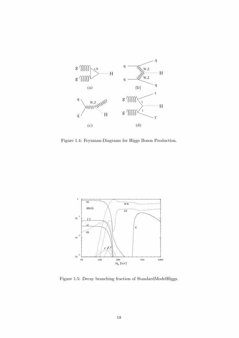
As shown in Figure 1.2, four experiments are proposed and being constructed. Two exper-
iments (ATLAS [1] and CMS) are for general purpose, one (ALICE) for heavy ion experiment
and one (LHCb) for b-physics experiment. One additional experiment (TOTEM), which hosts
on CMS, is an experiment to measure the total cross section, elastic scattering and diffractive
processes at the LHC.
12
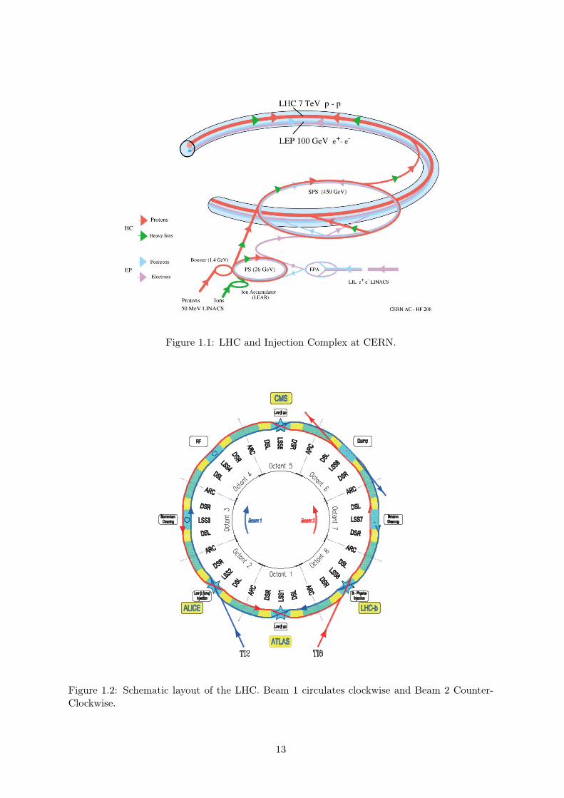
Figure 1.1: LHC and Injection Complex at CERN.
Figure 1.2: Schematic layout of the LHC. Beam 1 circulates clockwise and Beam 2 Counter-Clockwise.
13

Table 1.1: Parameters of the LHC.
Parameter Normal (High-Lumi.) Low-Lumi. Ultimate UnitCircumference 27 kmProton Energy 7.0 ← ← TeV
# of Protons/Bunch 1.1 0.17 1.67 1011
# of Bunch 2835 ← ←Bunch Spacing 25 ← ← ns
Current 0.56 0.087 0.850 ATrans. emittance 3.75 1.0 3.75 µradBeam size at IP 16 ← ← µradCrossing Angle 300 ← ← µrad
Luminosity 1.0 0.1 2.3 1034cm−2s−1
Life Time 10 ← ← HourFilling Time 3 ← ← Min
Table 1.2: Main Parameters of the dipole magnet.
Operational field 8.33 TCoil Aperture at 293K 56.00 mm
Distance between aperture axes at 1.9K 194.00 mmMagnetic length at 1.9K and at normal field 14312 mm
Current at normal field 11850 AOperating Temperature 1.9 K
1.1.2 The Bending (Dipole) Magnets in the LHC
In order to realize the highest beam energy with the given ring circumference, and also consid-
ering spatial limitation of the tunnel, superconducting dipole magnets [2], made with a special
technique, are employed in the LHC beam bending system. Due to the space constraint, (See
Figure 1.3) the magnet has two beam pipes for counter-rotating proton beams and provides an
anti-parallel magnetic field of 8.33 T for them. To realize such strong magnetic field, copper-
clad niobium-titanium windings are employed and they are operated under a temperature of
1.9 K with liquid helium. The parameters are summarized in Table 1.2. A total of 1,232
main dipole magnets will be installed in the ARC area, (see Figure 1.2) where the number is
maximized to achieve the highest energy. The cryogenics system for the magnets will contain
about 700 kl of liquid helium and have a power consumption of about 140 kW.
14

LHC Tunnel diameter = 3.8m
Warm helium recovery line
Helium ring line
LHC machine cryostat
Cryogenic distribution line (QRL)
Jumper connectionSpace reservedfor transport
Figure 1.3: Cross Section of LHC Tunnel with showing the LHC machine cross section.
1.2 Physics at the ATLAS Experiment
The ATLAS Experiment is designed to try to reveal the mechanism of electroweak symmetry
breaking and to study a variety of other physics which would appear at the TeV scale. In
particular, a Higgs boson, which is predicted in the Standard Model (SM), is able to be observed
in various decay channels over the full range of allowed mass region, if it exists. The ATLAS
Experiment can determine the Higgs mass and its couplings.
1.2.1 The Standard Model
The Standard Model (SM) is a very successful description of the interactions of the components
of matter at the smallest scales (< 10−18m) and highest energies (∼ 200GeV) accessible to
current experiments. It is constituted of a quantum field theory that describes the interaction
of spin-12 , point-like fermions, whose interactions are mediated by spin-1 gauge bosons.
The fermions consist of two groups: the leptons and the quarks. The leptons interact weakly
and electromagnetically (charged leptons only) and fall into three families,(eνe
) (µνµ
) (τντ
)
The quarks interact electromagnetically, weakly and strongly and fall into three families,(ud
) (cs
) (tb
)
Both the leptons and quarks have their own anti-particles. All mesons and baryons are com-
posed of the quarks and anti-quarks.
15

Table 1.3: Fundamental Forces and their Bosons.
Forces Boson Symbol Relative Strengthweak intermediate vector bosons W±, Z0 αweak = 1.02 × 10⁻⁵
electromagnetic photon γ αem = 1/137strong gluons g αstrong ≈ 0.1
There are three fundamental forces; the electromagnetic, weak and strong forces.1 They
are described by means of gauge theories and the forces are mediated by one or more boson(s).
They are summarized in Table 1.3.
In order to explain the spontaneous symmetry breaking in the electroweak sector, Higgs
mechanism, which provides masses to the W and Z bosons, has been introduced. The mech-
anism employs a spin-less particle called “the Higgs boson” in its minimal formulation. This
particle can also provide the masses of all the fermions in the SM.
1.2.2 Physics Potential
From an estimated non-diffractive cross-section of ∼100 mb [1], an average of 23 events are
expected per bunch crossing at the peak luminosity. They are mainly from QCD soft collision
processes, involving small momentum transfer, with spectator quarks. The events, which are
collected with the minimum-bias trigger, can be used to study the topological shapes and
energy flows of the events as a test of QCD. Jet cross-sections can be also investigated over
several orders of magnitude. More interesting events, such as a Higgs boson is produced, are
several orders of magnitude (10−13) less frequent. Among the various important physics [3],
the followings can be exploited in the ATLAS Experiment [1] :
• Higgs Boson:
One of the most important issues in the ATLAS Experiment is an approach to the ori-
gin of the spontaneous symmetry breaking in the electroweak sector in the SM and to
understand the origin of particle masses. The LHC has a capability of the Higgs boson
production for wide range of its mass (mH) from mH ≈ 80 GeV up to mH ≈ 1 TeV.
• Top Quark:
The LHC is a top quark factory. It produces roughly 107tt pairs per year even at the
moderate luminosity of 1033 cm−2s−1 (at low luminosity). The mass of the top quark can
be measured with an accuracy of about ±2GeV at a mass of mt ≈ 170 GeV.
• B-Physics:
In the ATLAS Experiment, a large number of B mesons are available for the studies of the
B-physics. The main purposes of the studies are precise measurements of CP violation1Gravitational force is not considered in this context.
16

in the b-quark system (B0d) and the determination of the angles of the unitary triangle
derived from the unitarity of the Cabibbo-Kobayashi-Maskawa matrix. In addition, it is
also possible to measure BsBs mixing and to search for rare decays such as B → µµ.
• Supersymmetric particles:
Supersymmetric extensions of the SM predict a wide spectrum of new particles with
masses and production rates such that at the LHC they could be discovered over a large
fraction of the parameter space. Events with a high jet multiplicity and large missing
energy make a search possible in the range of 1 to 4 TeV.
• Physics beyond the SM:
While the existing precision electroweak measurements are consistent with a light Higgs
boson, the possibility of electroweak symmetry breaking by new strong dynamics at the
TeV scale cannot be excluded. The following searches and measurements are proposed:
– Strongly interacting W’s.
– Technicolor.
– Compositeness.
– New Gauge Bosons.
– Extra Dimensions.
– Anomalous Gauge-boson Couplings.
1.2.3 Higgs Boson
The search for the Higgs boson is the most prominent issue for the LHC. It is used to optimize
the ATLAS detector geometry and is given here as an example of the physics potential. The
current limit on the Higgs mass from experiments at LEP [11] is mH > 113.5GeV.
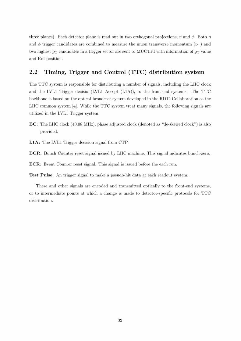
The Feynman-diagrams for Higgs boson production are shown in Figure 1.4. Over the mass
range of 80GeV < mH < 800GeV the gluon fusion (a) is dominant. The process (b) qq → qqH
becomes dominant for higher masses up to 1 TeV.
The decay branching fraction of standard model Higgs boson is shown in Figure 1.5. The
search strategy for the Higgs boson depend on its mass and several methods have to be combined
to cover the full mass range:
• H → bb :
With a Higgs boson mass below the threshold for decays into a pair of vector bosons, this
decay mode is essentially 100%. The signature used will be a lepton from one b-quark
and a b-quark jet from the other, possibly used with the associated production (Figure
1.4 (c) and (d)). This channel is sensitive at 80GeV < mH < 100GeV.
17
g
gH
(a)
q
q
H
q
q(b)
t,b W,Z
W,Z
q
q H
(c)
W,Z
(d)
H
t
t
t
t
g
g
Figure 1.4: Feynman-Diagrams for Higgs Boson Production.
BR(H)
bb_
Ą+Ą
cc_
gg
WW
ZZ
tt-
ƒÁƒÁZƒÁ
MH [GeV]50 100 200 500 1000
10-3
10-2
10-1
1
Figure 1.5: Decay branching fraction of StandardModelHiggs.
18

• H → γγ :
This is a sensitive channel for 90GeV < mH < 150GeV and requires an excellent electro-
magnetic calorimeter and identification of photons against a huge background from jets
misidentified as photons.
• H → ZZ(∗) → 4l± :
For masses between 130GeV < mH < 2mZ, one of the Z bosons is virtual and the Higgs
boson is rather narrow with a large background from boson pair production. For masses
mH > 2mZ, both bosons are real and the signal is rather clean.
• H → WW, ZZ → l±νjj, 2l±jj :
These signatures are important in the mass range up to mH ≈ 1TeV and uses two jets
for identification.
1.3 The ATLAS Detector
ATLAS [3] is a general-purpose proton-proton collider detector, which is being constructed for
LHC. It is designed to exploit the full discovery potential of the LHC. At the high luminosity,
integrated luminosity amounts 100fb−1 per year. Detectors and front-end electronics are firmly
required to be radiation tolerance for these high luminosities. 2 Furthermore, bunches of proton
are separated by only 25 ns, then high speed operations and low dead time of response are
strongly demanded on the detectors. In particular, the very first section of the ATLAS Trigger
system (LVL1 Trigger) is required to have low latency and no dead-time for its operation, which
will be discussed in the Chapter 2.
1.3.1 Overview
The ATLAS detector is illustrated in Figure 1.6, and it measures 22 m high, 44 m long, and
weighs 7,000 tons. The characteristics of the ATLAS detector are summarized as follows:
• Precision inner tracking system (denoted as “Inner Detector”) is constituted with pixel,
strip of silicon, and TRT with 2 T solenoidal magnet. Good performance is expected on
the B−tagging and the γ−conversion tagging.
• A very good electromagnetic calorimeter is mounted to identify and measure electrons
and photons.
• 4π-covered hadronic calorimeter for hermetic jet measurement and missing transverse
energy.
• A stand-alone muon spectrometer with toroidal magnets to identify muons and measure
their momentum.2This issue is discussed in the section 4.4.
19

Figure 1.6: The ATLAS detector overview.
1.3.2 Inner Detector
The inner detector is in an axial central field of 2 T provided by a superconducting solenoidal
magnet and measures the paths of electrically charged particles. The inner detector system
consists of following detectors:
• The pixel detector is based on silicon detectors which contain an array of pixel diodes.
The size of pixel is 50 µm × 400 µm.
• The SemiConductor Tracker (SCT) uses strip detectors with fine granularity in the φ
direction. Silicon is foreseen in the barrel region and GaAs substrates in the forward
region where the radiation doses are higher.
• The Transition Radiation Tracker (TRT) is based on straw tubes of 4mm diameter. The
straws are interleaved with polyethylene radiators to produce and detect X-ray emission
from very relativistic particles.
1.3.3 Calorimetry
The ATLAS detector has, like most colliding-beam high-energy beam experiments, two types of
calorimeters: an electromagnetic calorimeter situated directly outside of the solenoid magnet of
the inner detector, and a hadronic calorimeter is surrounding the electromagnetic one. (Shown
in Figure 1.8.) Accurate jet energy measurement and excellent missing energy reconstruction
20

TRT
Pixels SCT
Barrelpatch panels
Services
Beam pipe
Figure 1.7: Inner Detector.
requirements demand large rapidity coverage. The ATLAS calorimeters therefore extend up to
|η| = 4.9.
1.3.3.1 Electromagnetic Calorimeter
The electromagnetic (EM) calorimeter is a lead-liquid argon detector with accordion-shaped
Kapton electrodes and lead absorber plates over its full coverage. The accordion geometry
provides complete φ symmetry without azimuthal cracks. The lead thickness in the absorber
plates has been chosen as a function of rapidity, so as to optimize the calorimeter performance
in terms of energy resolution.
The total thickness of the EM calorimeter, which is shown in Figure 1.9 as a function of
rapidity, is above 24 radiation length(X0) in the barrel and above 26 X0 in the end-caps. The
EM calorimeter is segmented into square towers of size ∆η ×∆φ = 0.025× 0.025 (∼ 4× 4cm2)
at η = 0. The electromagnetic calorimeter is designed to keep the energy resolution at the level
of ∼ 10%/√
E(GeV) or below.
1.3.3.2 Hadronic Calorimeter
The ATLAS hadronic calorimeter covers the range |η| < 5 using different techniques and
devices as best suited for the different requirements and radiation environment. In the range
|η| < 1.6 the iron-scintillating-tiles technique is used for the barrel and extended barrel Tile
calorimeters and for partially instrumenting the crack between them with the Intermediate
Tile calorimeter (ITC). This gap provides space for cables and services from the innermost
detectors. In the range ∼ 1.5 < |η| < 4.9 the liquid argon calorimeter takes over: the end-cap
hadronic calorimeter extends till |η| < 3.2 while the range 3.2 < |η| < 4.9 is covered by the
high-density forward calorimeter.
21

Calorimeters
Calorimeters
Calorimeters
Calorimeters
Hadronic Tile
EM Accordion
Forward LAr
Hadronic LAr End Cap
Figure 1.8: Layout of the Calorimeters.
0
10
20
30
40
0 1 2 3Pseudorapidity
X0
Barrel-Endcap crack
PresamplerScintillator
ID services+ patch panel
warm flangecables + passive liquidMaterialin front of Presampler
Materialin front of Accordion
B A R R E L E N D C A P
Materialin front ofAccordion
Material up to the end of active BarrelMaterial up to the end of active Endcap
Total active depth
Figure 1.9: Total thickness (in radiation length)of the ATLAS EM calorimeter as a function ofη.
0
5
10
15
20
0 1 2 3 4 5Pseudorapidity
Abso
rptio
n Le
ngth
Tile barrel
Tileextended barrel Hadronic endcap Forward calorimeter
EM barrel EM endcap
Material in front of Muon System
End of activehadronic
cryostat walls
Figure 1.10: Amount of material (absorptionlength) in the ATLAS Calorimetry as a functionof η.
22

The total thickness is 11 interaction lengths (λ) at η = 0, including 1.5λ of the outer
support, sufficient to reduce the punch-through below the irreducible level of prompt or decay
muons. Figure 1.10 shows the amount material in the ATLAS calorimetry as a function of η
(including EM calorimeter). Together with the large η coverage this thickness will guarantee
a good EmissT measurement important in many physics signatures and in particular for SUSY
particle searches.
The most stringent transverse granularity requirement comes from the W → jet-jet decay at
high-pT and applies for |η| < 3 (barrel and end-cap), where a granularity ∆η ×∆φ = 0.1× 0.1
is needed. At these regions, the required energy resolution criteria are:
∆E
E=
50%√E
⊕ 10%.
This resolution is adequate to the tasks of providing jet reconstruction and jet-jet mass recon-
struction as well as missing pT measurement for physics process of interest.
In ATLAS the forward calorimeter (|η| > 3) is integrated in the end-cap cryostat, with the
front face at about 5 meters from the interaction point; this provides a clear benefit in terms of
uniformity of coverage, reducing to the minimal possible level the effects of the crack and dead
space in the transition region around η = 3.1, with advantages for the efficiency of forward jet
tagging and for the reduction of the tails in the EmissT distribution. For this forward calorimeter,
a granularity ∆η × ∆φ = 0.2 × 0.2 is sufficient and required energy resolution criterion is:
∆ET
ET=
100%√E
⊕ 10%.
1.3.4 Muon Spectrometer
The ATLAS muon spectrometer is based on a superconducting air-core toroid magnet system,
producing an average magnetic field of 0.5T, which consists of a 26 m long barrel part with an
inner bore of 9.4 m and an outer radius of 19.5 m and two end-caps with lengths of 5.6 m and
inner bores of 1.26 m. Each toroid consists of eight flat coils symmetrically arranged around
the beam axis with the end-caps rotated with respect to the barrel so that the coils interleave.
Muon chamber planes are attached to the toroids to measure the trajectories of muons. In
the barrel the layout consists of three layers of chambers and in the end-caps the chambers are
placed on the front and back faces of the cryostats. A third layer is fixed on the cavern wall.
Two types of chambers are used for the high-precision measurements: Monitored Drift Tube
chambers (MDT) and Cathode Strip Chambers (CSC).
The high-precision measurements are complemented with chambers for triggering. There
are also two types used for this: Resistive Plate Chambers (RPC) and Thin Gap Chambers
(TGC).
23

2
4
6
8
10
12 m
00
Radiation shield
MDT chambers
End-captoroid
Barrel toroid coil
Thin gap chambers
Cathode strip chambers
Resistive plate chambers
14161820 21012 468 m
Figure 1.11: R-Z View of the ATLAS Muon Spectrometer.
1.3.4.1 Monitored Drift Tube (MDT)
The Monitored Drift Tube chamber (MDT) consists of multi-layers of drift tubes with a diam-
eter of 30 mm as shown in Figure 1.12. The MDTs use non-flammable Ar(93%)/CO2(7%) gas
at 3 atm. Maximum drift time is 500 ns and position resolution is 80 µm.
Longitudinal beam
In-plane alignment
Multilayer
Cross plate
Figure 1.12: The MDT (Monitored Drift Tube).
1.3.4.2 Cathode Strip Chamber (CSC)
The Cathode Strip Chamber (CSC) is a multi-wire proportional chamber (MWPC) with a
symmetric cell in which the anode-cathode spacing is equal to the anode wire pitch, which
has been fixed at 2.54 mm. (Figure 1.13) In a CSC the precision coordinate is obtained by
measuring the charge induced on the segmented cathode by the avalanche formed on the anode
24

wire. The CSCs can be operated in highest rate environment at large η using an appropriate
segmentation. (cf. Figure 1.11)
Wires
Strips
Rohacell
Cathode read-out
Spacer bar
Sealing rubber Epoxy
Wire fixation bar
Conductive epoxy
HV capacitor
Anode read-out
Gas inlet/
outlet
0.5 mm G10
laminates
Nomex honeycomb
Figure 1.13: The CSC (Cathode Strip Tube).
1.3.4.3 Resistive Plate Chamber (PRC)
The Resistive Plate Chamber is a trigger chamber and used in the barrel region. The RPC
is the gaseous parallel plate detectors with two bakelite plates coated with layers of graphite
paint providing the electric field and external pick-up strips on plastic material for the signal.
A set of two orthogonal strips is used to provide two-dimensional information with good spatial
resolution.
Figure 1.14: The RPC (Resistive Plate Chamber).
25

1.3.4.4 Thin Gap Chamber (TGC)
The Thin Gap Chamber (TGC) is a trigger chamber used in the end-cap region. The TGC has
a structure similar to Multi-Wire Proportional Chambers (MWPCs), except that the anode-
to-anode, i.e. wire-to-wire, distance is larger than the cathode-to-anode distance. Figure 1.15
shows the TGC structure. This thin gap gives shorter drift time and high time resolution. Two
graphite cathodes with distance of 2.8 mm are sandwiched with 50 µm diameter Au-coated
anode wires with a pitch of 1.8 mm. The pick-up strips are formed in orthogonal direction to
the wires and this gives two-dimensional information.
To match the geometric granularity to the needed momentum resolution, from 4 to 20
anode wires are grouped and these wire-groups give R coordinates. The strips are readout
individually and give φ coordinates.
With the use of a highly quenching gas mixture of CO2 and pentane (C5H12), 55% : 45%
, this type of cell geometry allows operation in saturated mode. Saturated mode operation
enables the operation with the hit-rate of 1 kHz/cm2, which is ten times greater than the
estimated hit-rate at the ATLAS Experiment.
Since the TGC is too thin to satisfy the deformation requirement (maximum allowable
deformation is less than 100 µm), two or three TGCs sandwiches thick paper honeycombs. A
module with two TGCs denotes doublet and three TGCs one denotes triplet.
Figure 1.16 shows the cross-sections of triplet (left) and doublet of TGCs.
1.8 mm
1.4 mm
1.6 mm G-10
50 ∝ m wire
Pick-up strip
+HV
Graphite layer
Figure 1.15: TGC structure showing anode wires, graphite cathodes, G-10 layers, and read-outstrip orthogonal to the wires.
26

Figure 1.16: Cross-section of a triplet (left) and of a doublet of TGCs (right).
27

Chapter 2
The ATLASTrigger/Data-Acquisition (TDAQ)System
The ATLAS Trigger and Data-Acquisition (TDAQ) system is based on three levels of online
event selection. Each trigger level refines the decisions made at the previous level and, where
necessary, applies additional selection criteria. Starting from an initial bunch-crossing rate of
40.08 MHz (interaction rate ∼ 109 Hz at a luminosity of 1034 cm−2s−1), the rate of selected
events must be reduced to ∼ 100 Hz for permanent storage. While this requires an overall
rejection factor of 107 against “minimum-bias” processes, excellent efficiency must be retained
for the rare new physics, such as Higgs boson decays, that is sought in ATLAS.
Figure 2.1 shows a simplified functional view of the ATLAS TDAQ system. In the following,
a brief description is given of some of key aspects of the event-selection process.
The Level-1 (LVL1) Trigger system makes an initial selection based on reduced-granularity
information from the calorimeter (e, γ, jet, EmissT ) and muon detector(µ). High transverse-
momentum (high-pT) muons are identified using only the trigger chambers [7]. The calorimeter
selections are based on reduced-granularity information from all the ATLAS calorimeters (elec-
tromagnetic and hadronic; barrel, end-cap and forward) [8], [9].
The maximum rate at which the ATLAS front-end systems can accept LVL1 Trigger is
limited to 75 kHz (upgradeable to 100 kHz).
An essential requirement on the LVL1 Trigger is that it should uniquely identify the bunch-
crossing of interest. Given the short (25 ns) bunch-crossing interval, this is a non-trivial con-
sideration. In the case of the muon Trigger, the physical size of the muon spectrometer implies
times-of-flight comparable to the bunch-crossing period. For the calorimeter Trigger, a serious
challenge is that the pulse shape of the calorimeter signals extends over many bunch crossings.
It is important to keep the latency (time taken to form and distribute the trigger decision)
to a minimum. During this time period, information for all detector channels has to be re-
tained in “pipeline” memories. These memories are generally contained in custom integrated
28

LEVEL 2TRIGGER
LEVEL 1TRIGGER
CALO MUON TRACKING
Event builder
Pipelinememories
Derandomizers
Readout buffers(ROBs)
EVENT FILTER
Bunch crossingrate 40 MHz
< 75 (100) kHz
~ 3 kHz
~ 200 Hz
Interaction rate~1 GHz
Regions of Interest Readout drivers(RODs)
Full-event buffersand
processor sub-farms
Data recording
~ 10 ms
~ 1 s
~ 300MB/s
Figure 2.1: Schematic diagram of the ATLAS Trigger and DAQ System.
circuits, placed on or close to the detector, usually in inaccessible regions and in a high-radiation
environment. The total number of detector channels, excluding the pixel detectors, exceeds
107. For reasons of cost and reliability, it is desirable to keep the pipeline lengths as short as
possible. The LVL1 latency, measured from the time of the proton-proton collision until the
trigger decision is available to the front-end electronics, is required to be less than 2.5 µs. In
order to achieve this, the LVL1 Trigger is implemented as a system of purpose-built hardware
processors. The target latency for the LVL1 Trigger is 2.0 µs (leaving 500 ns contingency).
Events selected by LVL1 are read out from the front-end electronics systems of the detectors
and put into readout buffers (ROBs). A large number of front-end electronics channels are
multiplexed into each ROB. Intermediate buffers, labeled “derandomizer” in Figure 2.1, average
out the high instantaneous data rate at the output of the pipeline memories to match the
available input bandwidth of the readout drivers (RODs).
All of the data for the selected bunch crossing from all of the detectors are held in the
ROBs either until the event is rejected by the Level-2 (LVL2) Trigger (in which case the data
are discarded) or, in case the event is accepted by LVL2, until the data have been successfully
transferred by the DAQ system to storage associated with the Event Filter (which makes the
third level of event selection). The process of moving data from the ROBs to the Event Filter
(EF) is called event building. Whereas before event building each event is composed of many
fragments, with one fragment in each ROB, after event building the full event is stored in a
single memory accessible by an EF processor.
The LVL2 Trigger makes use of “region-of-interest” (RoI) information provided by the
29

LVL1 Trigger. This includes information on the position (η and φ) and pT range of candidate
objects (high-pT muons, electrons/photons, hadrons/taus, jets), and energy sums (missing-ET
vector and scalar ET value, where ET is transverse energy). The RoI data are sent by LVL1
to LVL2, for all events selected by the LVL1 Trigger, using a dedicated data path. Using the
RoI information, the LVL2 Trigger selectively accesses data from the ROBs, moving only the
data that are required in order to make the LVL2 decision. The LVL2 Trigger has access to
all of the event data, if necessary with the full precision and granularity. Thanks to this RoI
mechanism, usually only a few per cent of the full event data are required. The LVL2 Triggers
are required to reduce the rate to ∼3 kHz. The latency of the LVL2 Trigger is variable from
event to event; it is expected to be ∼10 ms.
After LVL2, the last stage of selection is performed in the EF. Here the algorithms will
be based on the offline code. The EF must reduce the rate to a level suitable for permanent
storage (∼300 MB/s), currently assumed to be ∼200 Hz for full events of size ∼1.5 Mbyte.
2.1 Level-1 (LVL1) Trigger Overview
Muon Trigger / CTPInterface
Central Trigger Processor
TTC
Muon Trigger(RPC based)
Muon Trigger(TGC based)
Front-end Preprocessor
Cluster Processor(electron/photon andhadron/tau triggers)
Jet/Energy-sumProcessor
Calorimeter Trigger Muon Trigger
Endcap Barrel
Trigger decision tofront-end, readoutand other systems
RoI information toLVL2 trigger
Read-out data to DAQsystem (ROBs)
Figure 2.2: ATLAS LVL1 Trigger System.
The LVL1 Trigger is one of the most essential parts of the ATLAS Experiment for the
reason that it decides whether the event is interest or not at the very early stage. As described
above, the LVL2 Trigger only searches selected region by LVL1 Trigger. Therefore, if the LVL1
Trigger makes failure, there is no way to salvage significant events at any following stages.
The LVL1 Trigger system is a system of synchronous, pipelined processors running at 40.08
MHz or multiples thereof. As shown in Figure 2.2, the LVL1 Trigger system is composed of
a number of building blocks: the calorimeter Trigger, the muon Trigger, the Central Trigger
Processor (CTP) and the Timing, Trigger and Control (TTC) system.
30

In the muon Trigger, both TGC based Endcap muon Trigger subsystem and RPC based
Barrel muon Trigger subsystem are operating in parallel. Each result of both muon Trigger
subsystem are gathered by the Muon Trigger CTP Interface (MUCTPI) and combined data
from all muon trigger chambers are sent to the CTP.
In the calorimeter Trigger, both Cluster processor and Jet/Energy processor are operating
in parallel and these results are sent to CTP individually.
2.1.1 Muon Trigger
The Level-1 muon Trigger is based on dedicated, fast and finely segmented muon detectors.
The layout of these trigger chambers, RPC detectors in the barrel regions and TGC detectors
in the end-cap regions are shown in Figure 2.3. RPC Trigger system covers the pseudorapidity
range |η| < 1.05, while the TGC Trigger system covers 1.05 < |η| < 2.4. In order to prevent
punch-through muons, RPC and TGC are overlapped at boundary region around |η| = 1.05.
The double counting of muon tracks introduced by this overlap will be solved at MUCTPI.
low pT
high pT
5 10 15 m0
RPC 3
RPC 2
RPC 1 low pT
high pT
MDT
MDT
MDT
MDT
TGC 1
TGC 2
TGC 3
MDT
MDT
Troidal Magnet
Figure 2.3: Layout of the ATLAS Muon Trigger Chambers.
There are troidal magnets at both end-cap and barrel regions creating rotating fields in φ
direction for bending muon tracks. (These troidal magnets are shown in Figure 1.11.) These
trigger chambers measure muon tracks.
As illustrated in Figure 2.3, the LVL1 muon Trigger is based on three trigger stations. Two
stations are used for low-pT muon riggers (threshold range approximately 6-10 GeV), while
the third station is used in addition for high-pT triggers (threshold range approximately 6-35
GeV)1. High-pT triggers are made by using the results of low-pT triggers. If high-pT trigger
candidates are found, they override the corresponding low-pT trigger candidates. Each station
is composed of two detector planes (with the exception of the innermost TGC station that has1For TGC, lower threshold of high-pT triggers had been extended down to 6 GeV.
31
three planes). Each detector plane is read out in two orthogonal projections, η and φ. Both η
and φ trigger candidates are combined to measure the muon transverse momentum (pT) and
two highest pT candidates in a trigger sector are sent to MUCTPI with information of pT value
and RoI position.
2.2 Timing, Trigger and Control (TTC) distribution system
The TTC system is responsible for distributing a number of signals, including the LHC clock
and the LVL1 Trigger decision(LVL1 Accept (L1A)), to the front-end systems. The TTC
backbone is based on the optical-broadcast system developed in the RD12 Collaboration as the
LHC common system [4]. While the TTC system treat many signals, the following signals are
utilized in the LVL1 Trigger system.
BC: The LHC clock (40.08 MHz); phase adjusted clock (denoted as “de-skewed clock”) is also
provided.
L1A: The LVL1 Trigger decision signal from CTP.
BCR: Bunch Counter reset signal issued by LHC machine. This signal indicates bunch-zero.
ECR: Event Counter reset signal. This signal is issued before the each run.
Test Pulse: An trigger signal to make a pseudo-hit data at each readout system.
These and other signals are encoded and transmitted optically to the front-end systems,
or to intermediate points at which a change is made to detector-specific protocols for TTC
distribution.
32
Chapter 3
The Endcap Muon (TGC) TriggerSystem
As described in Section 2.1.1, TGC provides the muon Trigger in the end-cap region. There are
two sides at the ATLAS detector. All ATLAS detector layouts and connections are arranged
as mirror symmetry, and there are no functional difference between both side Endcap muon
Trigger electronics.
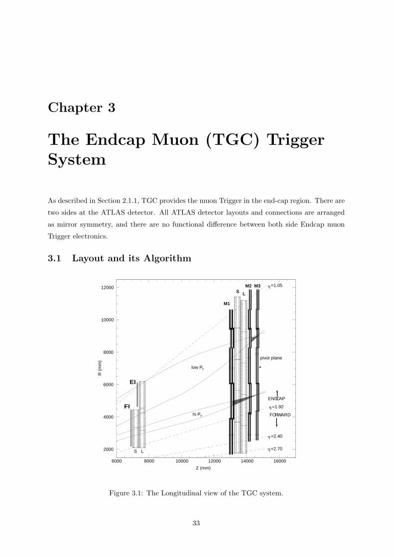
3.1 Layout and its Algorithm
2000
4000
6000
8000
10000
12000
6000 8000 10000 12000 14000 16000
EI
M1
M2 M3S L
=2.70
=1.05
=2.40
=1.92
Z (mm)
R (
mm
)
low PT
hi PT
pivot plane
ENDCAP
FORWARD
S L
FI
Figure 3.1: The Longitudinal view of the TGC system.
33

TGCs which cover end-cap region are layouted as Figure 3.1. Where EI (End-cap Inner),
FI (Forward Inner), M1, M2 and M3 are the station name of TGC planes. In M1 station,
triplet type TGCs are used and in M2 and M3 station, doublet type TGCs are used.(see Figure
1.16) M3 station is referred to as the pivot plane, and its chamber layout and electronics are
arranged such that, to a good approximation, there are no overlaps or holes in this plane. For
triggering, the TGCs cover a pseudorapidity range 1.05 < |η| < 2.4, except for the innermost
plane (EI/FI) which covers a range 1.05 < |η| < 1.9.
Figure 3.1 also shows the LVL1 muon Trigger scheme in the end-cap region. The trigger
algorithm uses pivot plane hits and extrapolates to the interaction point to construct the
apparent infinite-momentum path of the track. The deviation from this path of hits found
in the preceding “confirming” trigger planes is related to the track momentum. A window is
constructed for each trigger region in the r and φ directions around the infinite momentum path.
A coincidence is signaled if there is a hit in the window corresponding to the hit location in the
pivot plane. Independent signals are generated for R and φ, with the wire signals determining
the R-coordinate and strip signals determining φ-coordinate. The low-pT trigger is a trigger
candidate utilizes information from two doublets (M2 and M3). And the high-pT trigger is a
trigger candidate utilizes information low-pT trigger and triplet (M1). In order to have a good
trigger efficiency and an efficient background reduction, a 3-out-of-4 coincidence is required for
the doublet pair planes of M2 and M3, for both wires and strips, a 2-out-of-3 coincidence for
the triplet wire planes, and a 1-out-of-2 coincidence for the triplet strip planes is required.
Then the trigger windows are formed in R−φ space. Using these information, muon tracks
are classified into six levels of their transverse momentum (pT). The applied pT threshold is
determined by the size of the two-dimensional (R and φ) window, and for any single threshold
this window is optimized to provide 90% efficiency. Tracks are flagged according to the highest
threshold they cross. The final trigger decision in the end-cap system is done by merging the
results of the R − φ coincidence and the information from EI/FI chambers in order to reject
tracks coming from other than the interaction point. [13]
3.2 Implementation on the Electronics System
In this section, a detail description and its implementation of the Endcap muon Trigger system
along with the trigger path are given. Then, overview of readout system and DCS (Detector
Control System) issues are given in brief.
Figure 3.2 shows an overview of the TGC LVL1 Trigger electronics scheme and Figure
3.3 shows the placement of these electronics relative to the trigger chambers. The wire and
strip signals emerging from the TGC are fed into a two-stage amplifier in an Amplifier Shaper
Discriminator (ASD) circuit [23] [24]. Four ASD circuits are built into a single ASD chip
and four ASD chips are incorporated into an ASD Board; hence each ASD Board handles 16
34

channels of signals. The ASD Board is physically attached to the edge of a TGC and enclosed
inside the TGC electrical shielding.
KTR001V03
3 / 4 Coin. Matrix
triplet
innerdoublet
pivotdoublet
2 / 3 Coincidence
L1B De-rand
L1B De-rand
18
Patch Panel
BID, OR
BID, OR
BID, OR
BID, OR
BID, OR
BID, OR
BID, OR
ASD32
Wire Doublet Slave Board
Wire Triplet Slave Board
R
3 / 4 Coin. Matrix
triplet
innerdoublet
pivotdoublet
L1B De-rand
L1B De-rand
ϕ
20
Patch Panel
BID, OR
BID, OR
BID, OR
BID, OR
BID, OR
BID, OR
Strip Doublet Slave Board
Strip Triplet Slave Board
ASD32
ASD32
ASD32
ASD32
ASD32
ASD32
ASD32
ASD32
ASD32
ASD32
ASD32
ASD32
wire
strip
18
16
Wire High-pT Board
R, R
ϕ, ϕ
δ
δ
OR
SelectorH-Pt
L
H
Strip High-pT Board
SelectorH-Pt
L
H
SelectorH-Pt
L
H
SelectorH-Pt
L
H
CTP
EI wire
FI wire
EI strip
FI strip
L1B De-rand
4
Patch Panel
BID
BID
BID
BID
ASD32
FI Slave Boards
ASD32
ASD32
ASD32
4OR
OR
L1B De-rand
4
Patch Panel
BID
BID
BID
BID
ASD16
EI Slave Boards
ASD16
ASD32
ASD32
2OR
OR
Hits Selector
Sector Logic
R- ϕ Coin.M
UC
TP
I
TTC
F/E Electronics
Figure 3.2: Overview of the TGC LVL1 Trigger electronics system.
Signals from the ASD Boards are sent to a PS-Board where Patch-Panel (PP) ASICs and
Slave Board (SLB) ASICs are implemented. PS-Boards are placed on the accessible outer
surfaces of the TGC wheels except for EI/FI PS-Boards. Thus, electronics for the two doublets
are mounted on the outside of the outer doublet wheel and those for the triplets on the inner
surface of the triplet wheel. The PP ASIC has 32 channels of Bunch-Crossing Identification
(BCID) circuits. Outputs from PP are fed to the on-board logic to take care of physical overlap
35
in the TGCs and fan-outs.
The processed signals are sent to corresponding SLB ASICs where the coincidence and
read-out circuits are placed. There are five different types of SLB; wire and strip boards for
each of the triplet and doublets and a board for the EI/FI chamber. They differ in their number
of inputs, the kind of coincidence made and the maximum window width.
Information from the SLBs for the triplet and doublets is encoded to produce more compact
signals and the encoded coincidence information is passed to a High-pT coincidence Board
located near the outer rim of the triplet wheel. Signals from the doublet and triplet SLBs are
combined here to find high-pT track candidates. Wire (R-coordinate) and strip (φ-coordinate)
information is treated separately.
Signals from the High-pT Boards are sent to Sector Logic Boards containing an R-φ co-
incidence unit and track selectors, to select the highest-pT candidates. In the Sector Logic,
hit information from EI/FI SLBs is incorporated to the trigger logic. This provides excellent
robustness against soft charged particles due to the very large field integral produced by the
forward toroids located between the Trigger system and the innermost muon station. The Sec-
tor Logic boards are located in USA15 outside the main ATLAS cavern. The resulting trigger
information is sent to the MUCTPI in a standard format [16]. The total latency of the system,
from the bunch-crossing in which the interaction occurs until the delivery of the LVL1 track
candidates to the MUCTPI is 1.20 µs.
Full-information data sets are read-out through the DAQ system in parallel with the primary
trigger-logic. For read-out purposes the SLBs of one or more trigger sectors are grouped into
Local DAQ Blocks. Each SLB is connected to the Star Switch (SSW) which manages the
data collection for a Local DAQ Block. The transfer, via S-LINK (using optical fiber), of data
from the SSW witch to the Read Out Drivers (ROD) in USA15 is managed by the Local DAQ
Master.
The DCS has been developed on a ATLAS wide system to controle and monitor detec-
tors. The DCS is a slow path primarily for initial setting of the system and monitoring the
environment, power, gas flow, etc. TGC DCS is implemented by using the CAN-bus system.
3.3 Trigger Sector
Figure 3.4 shows the pivot plane formed by the TGC doublet plane furthest from the interaction
point. As shown in Figure 3.1 the pivot plane is divided into two regions, ENDCAP (|η| < 1.9)
and FORWARD (|η| > 1.9). The end-cap region of each octant (one eights of pivot plane)
is divided into six trigger sectors in φ, where a trigger sector is a logical unit that is treated
independently in the trigger. Similarly the Forward region of each octant is divided into three
trigger sectors. Thus in each side of TGC wheels, there are 48 ENDCAP trigger sectors and
24 FORWARD sectors.
36

High-Pt
Slave Board
Patch-panel
TGC EI
TGC EM1
TGC EM2 EM3Sector Logic
MUCTPI
MDT EMMDT EI
RO B
in USA15
Star-SW
in UXA15
Endcap toroid
Star-SW
Slave Board
Slave Board
Patch-panel
Patch-panel
RO D
TGC FI
Figure 3.3: TGC electronics placement.
In each trigger sector, the two highest-pT track candidates are selected and sent to the
MUCTPI.
The small region, shown by read dashed line in Figure 3.4 is a trigger subsector which
corresponds to the smallest unit area of the trigger segmentation. A trigger subsector corre-
sponds to eight channels of wire-groups and eight channels of readout strips. An ENDCAP
trigger sector contains 37 η rows by 4 φ columns, 148 trigger subsectors in total. A FORWARD
trigger sector contains 16 η rows by 4 φ columns, 64 trigger subsectors in total. Each trigger
subsector corresponds to one Region of Interest (RoI). Each subsector is treated independently
in the trigger so that the ∆r and ∆φ inputs that determine the pT condition applied can be
set separately for each subsector.
System segmentation is different between the detector and trigger logic. Each chamber
output is divided into 16-channel segments, corresponding to output from ASD boards (de-
scribed below). This segmentation, however, dose not correspond to the trigger segmentation
in wire-group signals since the chamber layout in R-directon shown in Figure 3.1 is not projec-
tive toward the interaction point. Hence the signals should be rearranged into proper segments
before entering trigger logic. Figure 3.5 shows the wire-signal segmentation. As shown in the
figure, trigger segments are over the boundaries of chambers, and signal exchanges are neces-
sary between them. This signal rearrangement is taken care of by PS-Boards. Totally 19 kinds
of PS-Boards are made and every signals are rearranged by rerouting and/or between adjacent
37

Figure 3.4: TGC LVL1 Trigger segmentation for an octant (one eights of pivot plane). One oc-tant wheel is divided into six ENDCAP sectors and three FORWARD sectors. Bold lines in thefigure indicate individual trigger sectors. They are further subdivided into trigger subsectors.
boards. For strip signals, the segmentation is same between the chamber and electronics and
no signal exchanges are needed. Details of signal rearrangement in PS-Boards are described in
“The TGC Excel Parameter Book” [25].
3.4 Latency
The total estimated latency of the Endcap muon Trigger system from interaction through to
the input to the MUCTPI is 1.20 µs. The contributions to this latency are listed in Table 3.1.
Adding the additional 12 bunch crossings for the MUCTPI and CTP, plus 20 bunch crossings
for the TTC and the cable back to front-end electronics, gives a total latency of 2.00 µs. This
meets the requirement of 2 µs and provides the full 0.5 µs contingency allocated within the 2.5
µs absolute maximum latency.
38

2000
4000
6000
8000
10000
12000
12000 12500 13000 13500 14000 14500 15000Z (mm)
R (m
m)
M1
M2 M3ā = 1.05
ā = 1.92
ā = 2.40
ā = 2.70
ā = 2.29ā = 2.16ā = 2.03
ā = 1.83
ā = 1.72
ā = 1.62
ā = 1.53
ā = 1.46
ā = 1.37
ā = 1.26
ā = 1.14
ā = 1.05
KHA051V01
Figure 3.5: Wire-signal segmentation. Each small box represents a segment of 32 channels,corresponding to 4 subsectors.
Table 3.1: contributions to the total estimated TGC latency, in bunch-crossing in number ofbunch crossing. (BC) (1 BC = 25 ns)
Process/transmission Time required Accumulated timeTOF to TGC 3 3TGC response 1 4ASD 1 5Cable to Patch Panel 2 7Bunch-crossing ID and OR (PP ASIC) 2 9Cable to SLB 0 9Delay Adjust (SLB ASIC) 1 103/4 or 2/3 coincidence (SLB ASIC) 3 13Cable to high-pT coincidence 3 16Delay adjustment (HPT ASIC) 1 17High-pT coincidence matrix (HPT ASIC) 4 21Optical cable to USA15 (90 m) 18 39Sector Logic processing 8 47Cable to MUCTPI (5 m) 1 48Total delay sum 48BC 1.20 µs
39

Chapter 4
System Development Issues
This section is devoted for both the discussions on technology selection and radiation tolerance
test, and the detailed design and its specification of the components which the author had
developed.
4.1 Technology selections for the system components
In this section, discussions on the requirements of choosing devices for each component are
described. As following reasons, we decided to use only ASIC and Anti-Fuse type FPGA for
electronics devices located in the experimental hall.
The FPGA (Field Programmable Gate Array) and the CPLD (Complexed Programmable
Logic Device) are popular devices and have convenient features such as; reprogrammable1, wide
line-up of its gate size and speed range, and availability. For this reason, the FPGA/CPLD
is widely used for today’s electronic circuits such as computers, networking equipments and
scientific instruments.
FPGAs and CPLDs have large configuration memories to determine its functionality. There
are two types of configuration memories: SRAM (volatile) and Flash (non-volatile). The con-
figuration data stored in the memories set properties of whole logic blocks and set connections
between logic cells and I/O ports.
It is known that bit-flip phenomenon of their configuration memories at high radiation
environment, and this may cause function failure of the device. Such data change can be found
by read-back the configuration data from the device periodically. Thus such a failure can be
fixed by re-configuring the device. Using this method (periodical read-back & re-configuration),
the system functionality can be retained except the read-back cycle duration2.
This technique sounds good idea, therefore at first TGC system planed to adopt both
SRAM-based FPGAs and Flash-based CPLDs for some components.3 However, we’ve found
1This means any circuit modifications can be done after the components made.2The period of read-back from each device should be determined in consideration of MTBF (Mean Time
Before Failure) by the modification of configuration memories and the number of this type of devices.3In that design, the read-back and re-configuration are done by using a Flash-based CPLD (non-volatile).
40
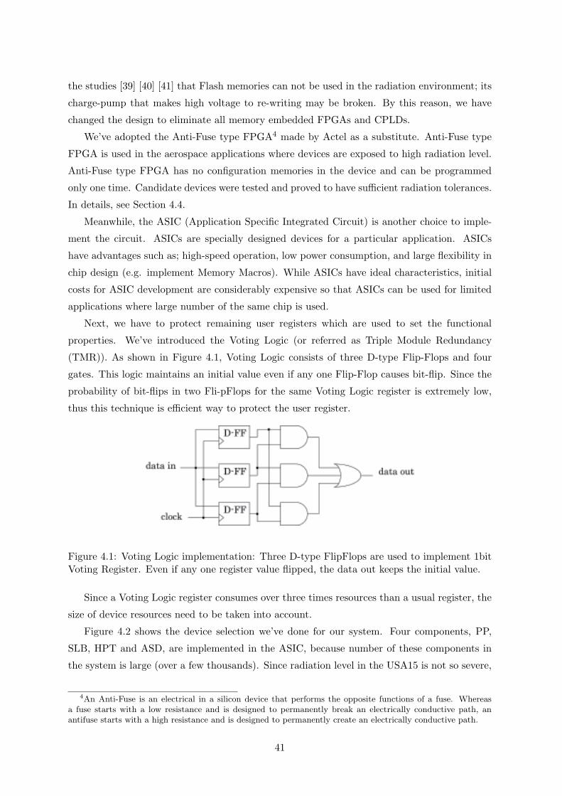
the studies [39] [40] [41] that Flash memories can not be used in the radiation environment; its
charge-pump that makes high voltage to re-writing may be broken. By this reason, we have
changed the design to eliminate all memory embedded FPGAs and CPLDs.
We’ve adopted the Anti-Fuse type FPGA4 made by Actel as a substitute. Anti-Fuse type
FPGA is used in the aerospace applications where devices are exposed to high radiation level.
Anti-Fuse type FPGA has no configuration memories in the device and can be programmed
only one time. Candidate devices were tested and proved to have sufficient radiation tolerances.
In details, see Section 4.4.
Meanwhile, the ASIC (Application Specific Integrated Circuit) is another choice to imple-
ment the circuit. ASICs are specially designed devices for a particular application. ASICs
have advantages such as; high-speed operation, low power consumption, and large flexibility in
chip design (e.g. implement Memory Macros). While ASICs have ideal characteristics, initial
costs for ASIC development are considerably expensive so that ASICs can be used for limited
applications where large number of the same chip is used.
Next, we have to protect remaining user registers which are used to set the functional
properties. We’ve introduced the Voting Logic (or referred as Triple Module Redundancy
(TMR)). As shown in Figure 4.1, Voting Logic consists of three D-type Flip-Flops and four
gates. This logic maintains an initial value even if any one Flip-Flop causes bit-flip. Since the
probability of bit-flips in two Fli-pFlops for the same Voting Logic register is extremely low,
thus this technique is efficient way to protect the user register.
Figure 4.1: Voting Logic implementation: Three D-type FlipFlops are used to implement 1bitVoting Register. Even if any one register value flipped, the data out keeps the initial value.
Since a Voting Logic register consumes over three times resources than a usual register, the
size of device resources need to be taken into account.
Figure 4.2 shows the device selection we’ve done for our system. Four components, PP,
SLB, HPT and ASD, are implemented in the ASIC, because number of these components in
the system is large (over a few thousands). Since radiation level in the USA15 is not so severe,
4An Anti-Fuse is an electrical in a silicon device that performs the opposite functions of a fuse. Whereasa fuse starts with a low resistance and is designed to permanently break an electrically conductive path, anantifuse starts with a high resistance and is designed to permanently create an electrically conductive path.
41

Experimental hallElectronics hut
PS-BoardHSC CrateASICASIC FPGA(Anti-fuse)FPGA(Anti-fuse)
Figure 4.2: Device selection at the TGC electronics system.
any FPGA can be used. In Section 4.3, the development of the Sector Logic, which is located
in the electronics hut, is described.
42
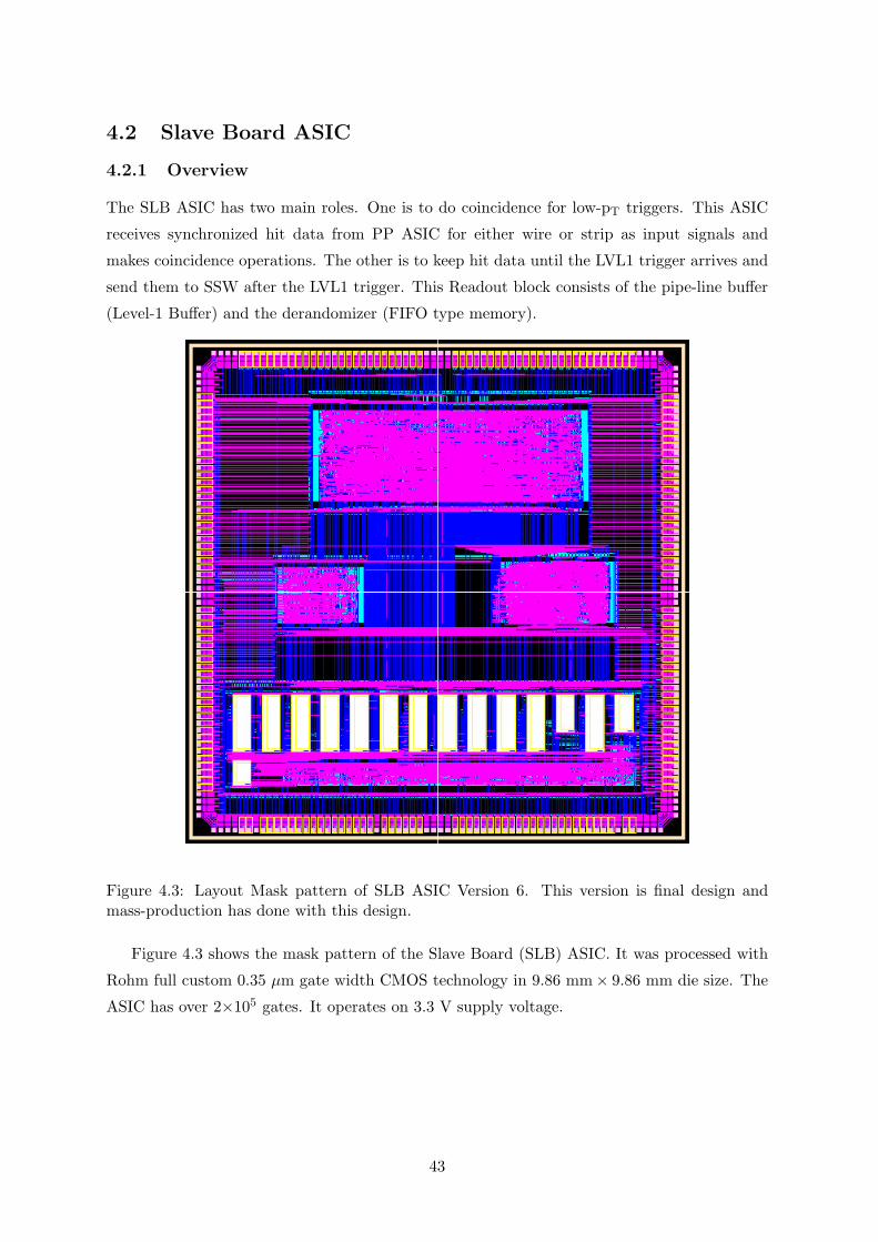
4.2 Slave Board ASIC
4.2.1 Overview
The SLB ASIC has two main roles. One is to do coincidence for low-pT triggers. This ASIC
receives synchronized hit data from PP ASIC for either wire or strip as input signals and
makes coincidence operations. The other is to keep hit data until the LVL1 trigger arrives and
send them to SSW after the LVL1 trigger. This Readout block consists of the pipe-line buffer
(Level-1 Buffer) and the derandomizer (FIFO type memory).
Figure 4.3: Layout Mask pattern of SLB ASIC Version 6. This version is final design andmass-production has done with this design.
Figure 4.3 shows the mask pattern of the Slave Board (SLB) ASIC. It was processed with
Rohm full custom 0.35 µm gate width CMOS technology in 9.86 mm× 9.86 mm die size. The
ASIC has over 2×10⁵ gates. It operates on 3.3 V supply voltage.
43
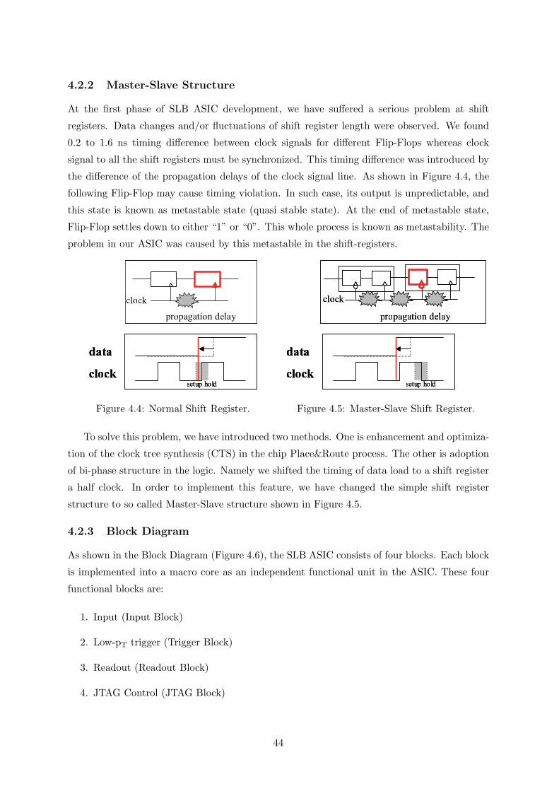
4.2.2 Master-Slave Structure
At the first phase of SLB ASIC development, we have suffered a serious problem at shift
registers. Data changes and/or fluctuations of shift register length were observed. We found
0.2 to 1.6 ns timing difference between clock signals for different Flip-Flops whereas clock
signal to all the shift registers must be synchronized. This timing difference was introduced by
the difference of the propagation delays of the clock signal line. As shown in Figure 4.4, the
following Flip-Flop may cause timing violation. In such case, its output is unpredictable, and
this state is known as metastable state (quasi stable state). At the end of metastable state,
Flip-Flop settles down to either “1” or “0”. This whole process is known as metastability. The
problem in our ASIC was caused by this metastable in the shift-registers.
dataclock
�z�ü�x��clockpropagation delay
setup hold
dataclock
�z�ü�x��clockpropagation delay
setup hold
Figure 4.4: Normal Shift Register.
setup hold
clockpropagation delay
dataclock
setup hold
clockpropagation delay
dataclock
Figure 4.5: Master-Slave Shift Register.
To solve this problem, we have introduced two methods. One is enhancement and optimiza-
tion of the clock tree synthesis (CTS) in the chip Place&Route process. The other is adoption
of bi-phase structure in the logic. Namely we shifted the timing of data load to a shift register
a half clock. In order to implement this feature, we have changed the simple shift register
structure to so called Master-Slave structure shown in Figure 4.5.
4.2.3 Block Diagram
As shown in the Block Diagram (Figure 4.6), the SLB ASIC consists of four blocks. Each block
is implemented into a macro core as an independent functional unit in the ASIC. These four
functional blocks are:
1. Input (Input Block)
2. Low-pT trigger (Trigger Block)
3. Readout (Readout Block)
4. JTAG Control (JTAG Block)
44

Figure 4.6: Block Diagram of the SLB ASIC.
The macro core structure can be seen from the picture of the ASIC layer mask pattern.
Several small squares regularly aligned at the bottom in Figure 4.3 are the macro cores for the
Readout block with the memory of 128 bits depth and 12, 20 or 32 bits widths while the single
large square at the top is for the input block. The small squares in the central part are the
JTAG control and the low-pT matrix blocks from left to right.
4.2.4 Input Block
The SLB ASIC can accept maximum 160 input signals from PP ASICs. In the Input block,
every individual channel can be masked in three different ways. The mask can be set as:
1. through input data (no mask),
2. always low (=0; force cold channel)
3. always high (=1; force hot channel)
Namely we have 2 bits mask for each channel. The mask registers can be accessed with the
standard JTAG protocol. In addition, we have two masks for one input channel; one for hit
signal stream (thus consequently for the trigger stream too) and the other one for only trigger
data stream. The concept of this double mask scheme for a channel is shown in Figure 4.7.
The “always high” logic can improve acceptance loss that comes from dead channels even if
one chooses the 4-out-of-4 coincidence logic. The “always low” logic is used to eliminate noisy
channels and unwanted channels for the trigger. The masking logic posterior to the phase-
adjust circuit has a function of a test pulse input. The test pulse is triggered by the Test Pulse
45
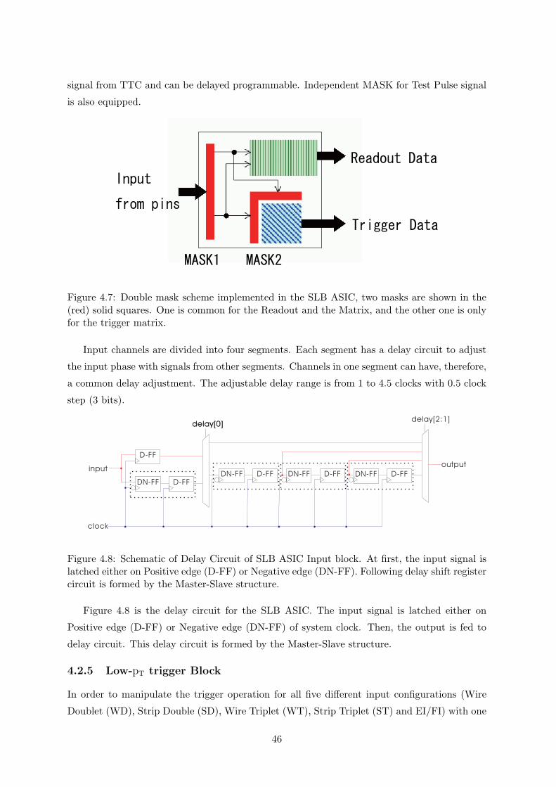
signal from TTC and can be delayed programmable. Independent MASK for Test Pulse signal
is also equipped.
Inputfrom pins
Readout Data
Trigger Data
MASK1 MASK2
Figure 4.7: Double mask scheme implemented in the SLB ASIC, two masks are shown in the(red) solid squares. One is common for the Readout and the Matrix, and the other one is onlyfor the trigger matrix.
Input channels are divided into four segments. Each segment has a delay circuit to adjust
the input phase with signals from other segments. Channels in one segment can have, therefore,
a common delay adjustment. The adjustable delay range is from 1 to 4.5 clocks with 0.5 clock
step (3 bits).
D-FF
DN-FF
inputDN-FF D-FF DN-FF D-FF DN-FF D-FF
clock
output
D-FF
delay[0]delay[0]delay[2:1]
Figure 4.8: Schematic of Delay Circuit of SLB ASIC Input block. At first, the input signal islatched either on Positive edge (D-FF) or Negative edge (DN-FF). Following delay shift registercircuit is formed by the Master-Slave structure.
Figure 4.8 is the delay circuit for the SLB ASIC. The input signal is latched either on
Positive edge (D-FF) or Negative edge (DN-FF) of system clock. Then, the output is fed to
delay circuit. This delay circuit is formed by the Master-Slave structure.
4.2.5 Low-pT trigger Block
In order to manipulate the trigger operation for all five different input configurations (Wire
Doublet (WD), Strip Double (SD), Wire Triplet (WT), Strip Triplet (ST) and EI/FI) with one
46

single ASIC, the Low-pT trigger block has three main logics, which are selectable by setting
appropriate registers. A coincidence matrix technique is used commonly for wire WD and
strip SD configurations while 2 out of 3 and 1 out of 2 (or) logics are used for WT and ST
respectively. EI/FI is used ST logic. In the following subsections, the implementations of these
logic are described.
4.2.5.1 Coincidence Matrix for Doublets pair (DSB)
The Doublet Slave Board (DSB) services the four layers of the two sets of TGC doublets. A
block diagram of the Doublet Slave Board is shown in Figure 4.9, where Phase adjust and
Masks are implemented in Input block (see Section 4.2.4) and L1 buffers, Derandomizer and
counters are implemented in Readout block (See Section 4.2.6) respectively.
SOS041V11
Mask
Phase adjust
Clock
Clock
3-out-of-4Coin. Matrix
Clock L1A
LS-Link
Derandomizer
Mask
Phase adjust
Phase adjust
Phase adjust
Phase adjust
Phase adjust
Phase adjust
Phase adjust
pivotdoublet
middledoublet
2x6
2x6
2x2
2x2
32
32
32
32
ƒÂ RPosition + 18-bit
ECR
BCR FE_BCID COUNTER
FE_L1ID COUNTER
L1 buffer
Mask
Mask
TestPulse
TestPulse
Figure 4.9: The functional structure of a Slave Board for the TGC doublet pairs. Shown is thewire Slave Board; the strip Slave Board has 16-bit output instead.
Each DSB covers a 32-channel per layer width of either wire or strip signals, giving 128
channels of inputs to a DSB from the four TGC layers. For wires, a track segment found by
the coincidence matrix is encoded as an 18-bit word containing R, its pivot plane position,
and ∆R, its deviation from the infinite momentum path. Similarly, for strips, a 16-bit word is
encoded containing φ and ∆φ information. If high background rates produce a large number
of accidental coincidences, the 3-out-of-4 coincidence matrix can be programmed to provide a
4-out-of-4 coincidence offering a more robust trigger.
47
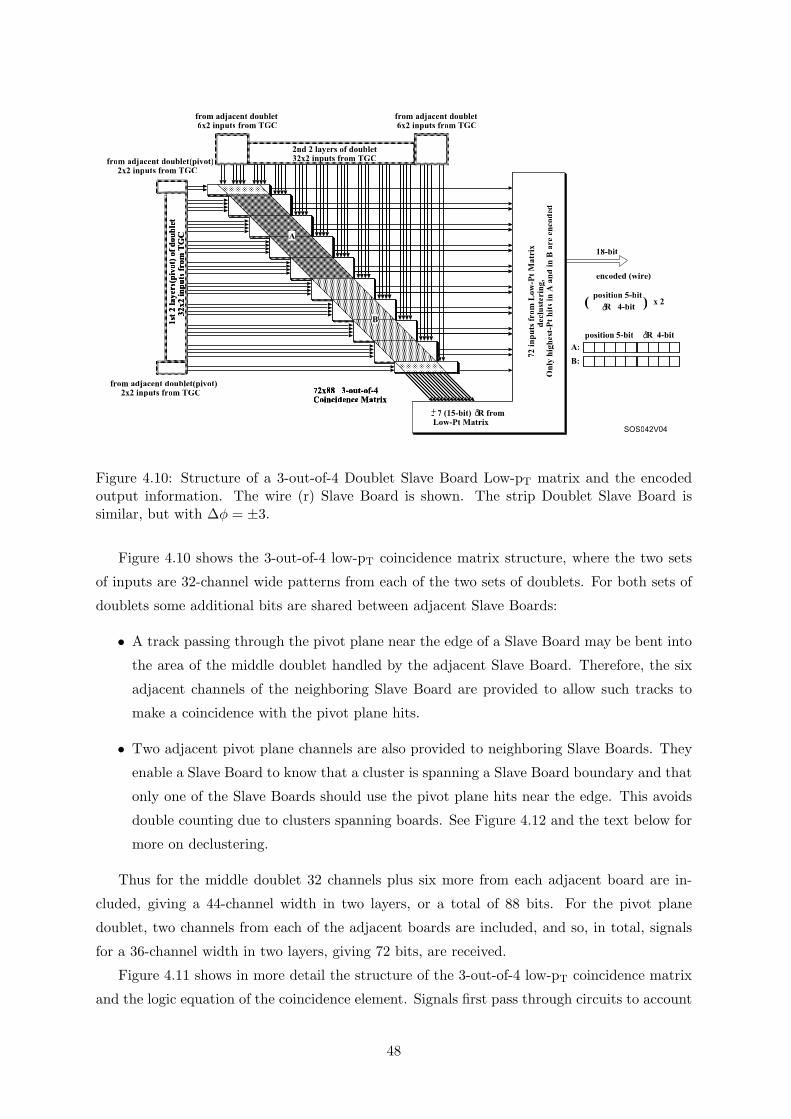
A
B
B
C
C
D
D
72x88 3-out-of-4Coincidence Matrix
1st 2
laye
rs(p
ivot
) of d
oubl
et
32x2
inpu
ts fr
om T
GC
2nd 2 layers of doublet32x2 inputs from TGC
from adjacent doublet 6x2 inputs from TGC
from adjacent doublet 6x2 inputs from TGC
a
d
from adjacent doublet(pivot) 2x2 inputs from TGC
from adjacent doublet(pivot) 2x2 inputs from TGC
72 in
puts
from
Low
Pt M
atrix
en
code
, hig
hest
Pt h
it
18-bit
encoded (wire)
72x88 3-out-of-4Coincidence Matrix
1st 2
laye
rs(p
ivot
) of d
oubl
et
32x2
inpu
ts fr
om T
GC
72 in
puts
from
Low
-Pt M
atrix
dec
luste
ring,
Onl
y hig
hest-
Pt h
its in
A an
d in
B ar
e enc
oded
position 5-bit R 4-bitƒÂ x 2( )
ƒÂR 4-bitposition 5-bit
A
B
A:B:
7 (15-bit) R fromLow-Pt Matrix
ƒÂ+-SOS042V04
Figure 4.10: Structure of a 3-out-of-4 Doublet Slave Board Low-pT matrix and the encodedoutput information. The wire (r) Slave Board is shown. The strip Doublet Slave Board issimilar, but with ∆φ = ±3.
Figure 4.10 shows the 3-out-of-4 low-pT coincidence matrix structure, where the two sets
of inputs are 32-channel wide patterns from each of the two sets of doublets. For both sets of
doublets some additional bits are shared between adjacent Slave Boards:
• A track passing through the pivot plane near the edge of a Slave Board may be bent into
the area of the middle doublet handled by the adjacent Slave Board. Therefore, the six
adjacent channels of the neighboring Slave Board are provided to allow such tracks to
make a coincidence with the pivot plane hits.
• Two adjacent pivot plane channels are also provided to neighboring Slave Boards. They
enable a Slave Board to know that a cluster is spanning a Slave Board boundary and that
only one of the Slave Boards should use the pivot plane hits near the edge. This avoids
double counting due to clusters spanning boards. See Figure 4.12 and the text below for
more on declustering.
Thus for the middle doublet 32 channels plus six more from each adjacent board are in-
cluded, giving a 44-channel width in two layers, or a total of 88 bits. For the pivot plane
doublet, two channels from each of the adjacent boards are included, and so, in total, signals
for a 36-channel width in two layers, giving 72 bits, are received.
Figure 4.11 shows in more detail the structure of the 3-out-of-4 low-pT coincidence matrix
and the logic equation of the coincidence element. Signals first pass through circuits to account
48

0
A B
CD
X
Y
X = Y = A & C + A & D + B & D
12x2 (middle doublet) inputs4x
2 (pi
vot d
oubl
et) i
nput
s
ƒÂR
8 out
puts
to en
code
r sec
tion
SOS043V05
b C = a & b & c + a & b & ca
c-1-2-3-4-5-6 76543217-
OR�
ed Y
OR�ed X
C
Figure 4.11: Detailed structure of the 3-out-of-4 Low-pT matrix for wires. Also shown is thefunction of a matrix element. Cells with the same shading have the same ∆r. The matrix forφ is the same, except ∆φ goes from -3 to +3. (Actually X and Y in the figure are the same.)
for the half-cell staggering between layers in order to improve the effective resolution. The
3-out-of-4 coincidence is then performed in each coincidence element. When a coincidence is
found, a hit signal and ∆R (or ∆φ) signal are generated. Hit signals in the elements of each
row are OR’ed, while the ∆R (or ∆φ) signals are OR’ed along the diagonal elements. For R,
the ∆R output pattern is 15 bits wide; for φ, the ∆φ output pattern is seven bits wide.
In Figure 4.10, the coincidence matrix is shown divided into two halves, A and B, (each half
services signals from a 16-channel per layer width) and the highest-pT track candidate found in
each half is selected. Hence the OR’ing mentioned above is done for each half independently.
To select the highest-pT track, ∆R (or ∆φ) outputs are examined first and then the selected
hits with the smallest |∆R| from the 3-out-of-4 coincidence are passed through declustering
logic to produce a single track. Figure 4.12 shows the declustering rules. Even though a real
particle almost always makes at most two hits, a cluster is treated as a single track, regardless
of its size. If more than one cluster is found in any half-matrix, only the highest-pT track
candidate is kept. For wires, the 15-bit ∆R pattern (∆R = −7 to ∆R = +7) is encoded in
four bits and position information is encoded in five bits so that the R information for each
track is nine bits wide. This encoding reduces the required number of cables and hence the
line-driver power dramatically. Since each of the two halves of the Slave Board can produce a
track candidate, the output from this circuit is 18 bits wide. For strips, the seven bit wide ∆φ
pattern (∆φ = −3 to ∆φ = +3) is encoded in three bits. Position in φ is encoded in five bits
49

Rule for Declustering
ABCDE
C-Output
C-Output = B & C & D + A & B & C
SOS044V03
Figure 4.12: Declustering rules. When a hit pattern wider than two is found, the rules shownassign a position to the track.
so that the φ information for each track is eight bits wide and for the two highest-pT tracks,
16 bits. Despite this attention to multi-muon encoding, the occurrence of more than one muon
in the area covered by a Slave Board is rare.
4.2.5.2 Triplet Slave Board (TSB)
The Triplet Slave Board (TSB) (Figures 12-18 and 12-20) performs coincidence operations on
signals from the three layers of the triplet. The TSB is similar to the Doublet Slave Board.
The wire coincidence operation uses 2-out-of-3, and the strip 1-out-of-2, logic. Figure 4.13
and Figure 4.15 show the TSB trigger-logic and Readout components for wires and strips
respectively.
Wire Triplet Slave Board: Each wire TSB receives from each layer of TGCs a 36-channel
wide wire pattern. It also includes two bits from each of the two adjacent boards to
take care of boundaries between regions covered by adjacent Slave Boards, resulting in
a 108-bit input pattern. The coincidence matrix is subdivided into three 32-channel
sections. The structure of the 2-out-of-3 coincidence for triplet wire signals and the logic
equation are shown in Figure 4.14. Signals first pass through circuits to account for the
cell-staggering of 1/3 between successive layers before they go through the coincidence
circuits. A 3-out-of-3 coincidence can also be required should the background rate be
50

SOS051V10
MaskClockClock L1A
LS-Link
Phase adjust
L1 buffer
Derandomizer
2-out-of-3
2-out-of-3 18-bitCoincidence
Phase adjust
Phase adjust
Phase adjust
Phase adjust
3x2
32
32
32
3x2
ECR
BCR FE_BCID COUNTER
FE_L1ID COUNTER
Mask
TestPulse
Figure 4.13: Slave Board for TGC Triplets (for wire signals).
36x3 (triplet) inputs
declustering and encoder 1 hit / 32 inputs
18 bits (3 hits) / Triplet Slave Board
hit position hit position hit position
100
C1
A1 A2B2B1
out
out = A1 & B2& C0& C2 + C1 & A1 & B1 + C1 & B2 & A2
C2C0
SOS052V06
Figure 4.14: Structure of the Triplet logic for wire signals. Logic to deal with the staggeringof triplet layers and the output format after encoding is also shown.
51
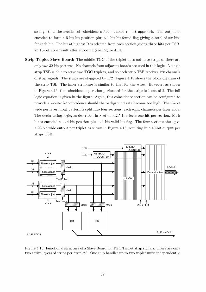
so high that the accidental coincidences force a more robust approach. The output is
encoded to form a 5-bit hit position plus a 1-bit hit-found flag giving a total of six bits
for each hit. The hit at highest R is selected from each section giving three hits per TSB,
an 18-bit wide result after encoding (see Figure 4.14).
Strip Triplet Slave Board: The middle TGC of the triplet does not have strips so there are
only two 32-bit patterns. No channels from adjacent boards are used in this logic. A single
strip TSB is able to serve two TGC triplets, and so each strip TSB receives 128 channels
of strip signals. The strips are staggered by 1/2. Figure 4.15 shows the block diagram of
the strip TSB. The inner structure is similar to that for the wires. However, as shown
in Figure 4.16, the coincidence operation performed for the strips is 1-out-of-2. The full
logic equation is given in the figure. Again, this coincidence section can be configured to
provide a 2-out-of-2 coincidence should the background rate become too high. The 32-bit
wide per layer input pattern is split into four sections, each eight channels per layer wide.
The declustering logic, as described in Section 4.2.5.1, selects one hit per section. Each
hit is encoded as a 4-bit position plus a 1 bit valid hit flag. The four sections thus give
a 20-bit wide output per triplet as shown in Figure 4.16, resulting in a 40-bit output per
strips TSB.
SOS054V08
Phase adjust
Phase adjust
MaskClock
LS-Link
L1 buffer
Derandomizer
OR
2x20 = 40-bit
Phase adjust
Phase adjust
Clock
Mask
OR
Clock L1A
32
32
32
32
ECR
BCR FE_BCID COUNTER
FE_L1ID COUNTER
Mask
Mask
TestPulse
TestPulse
Figure 4.15: Functional structure of a Slave Board for TGC Triplet strip signals. There are onlytwo active layers of strips per “triplet”. One chip handles up to two triplet units independently.
52

32x2 (triplet) inputs (no neighbor input)
declustering and encoder 1 hit / 16 inputs
20 bits (4 hits) / Triplet Slave Board
hit position hit positionhit position hit position
64
SOS053V04
out = b & c + b & a & c + a & c & b + c & b & d + b & d & cout
dcba
Figure 4.16: The functional structure of the triplet Slave Board for strip signals. Logic to dealwith the staggering of triplet layers and output format after the encoder section is also shown.
4.2.5.3 EI/FI Slave Board (EFSB)
The EI/FI Slave Board (EFSB) (Figure 4.17) performs coincidence operations (1-out-of-2) on
signals from the EI/FI doublet. The total numbers of the wire signals from an EI TGC doublet
unit and an FI TGC doublet unit are 16 and 32 per layer respectively. The total number of
the strip signals per layer is 32 for both the EI and FI TGC units. A single EFSB takes care
of signals from an EI or an FI doublet.
The EFSB has very similar structure to the TSB, as shown Figure 4.18. The additional
functionality of the EFSB is coincidence logic that provides hit-signals to the Sector Logic
boards. The Slave Board performs the 1-out-of-2 (or optionally 2-out-of-2) coincidence opera-
tion. Since the trigger window size in the EI/FI station is larger than 50 cm (in the bending
plane), fine granularity in the provision of hit-signals is not necessary. The segmentation for
the EI TGC unit is defined to be two segments in the R-direction and four segments in the
φ-direction. The FI TGC unit is subdivided into four segments in both the R and φ-directions.
Each segment provides a hit-signal using the coincidence logic shown in Figure 4.18. The total
number of the hit-signals sent to the Sector Logic is 6 bits per the EI TGC doublet and 8 bits
per the FI TGC doublet.
53

KHA021V02
Phase adjust
Phase adjust
MaskClock
LS-Link
L1 buffer
Derandomizer
OR
6-bit
Phase adjust
Phase adjust
Clock
Mask Clock L1A
32
32
32
32
wire
strip
OR OR OR OR OR OR OR
ECR
BCR FE_BCID COUNTER
FE_L1ID COUNTER
Mask
Mask
TestPulse
TestPulse
Figure 4.17: Slave Board for the EI/FI TGC doublet.
KHA023V01
EI / FI 32x2 inputs
OR
64
hit
OR
hit
OR
hit
OR
hitout = b & c + b & a & c + a & c & b + c & b & d + b & d & cout
dcba
Figure 4.18: The functional structure of the EI/FI Slave Board. Logic to deal with the stag-gering of doublet layers and output format after the encoder section is also shown.
54
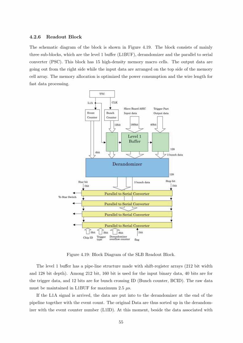
4.2.6 Readout Block
The schematic diagram of the block is shown in Figure 4.19. The block consists of mainly
three sub-blocks, which are the level 1 buffer (L1BUF), derandomizer and the parallel to serial
converter (PSC). This block has 15 high-density memory macro cells. The output data are
going out from the right side while the input data are arranged on the top side of the memory
cell array. The memory allocation is optimized the power consumption and the wire length for
fast data processing.
Figure 4.19: Block Diagram of the SLB Readout Block.
The level 1 buffer has a pipe-line structure made with shift-register arrays (212 bit width
and 128 bit depth). Among 212 bit, 160 bit is used for the input binary data, 40 bits are for
the trigger data, and 12 bits are for bunch crossing ID (Bunch counter, BCID). The raw data
must be maintained in L1BUF for maximum 2.5 µs.
If the L1A signal is arrived, the data are put into to the derandomizer at the end of the
pipeline together with the event count. The original Data are thus sorted up in the derandom-
izer with the event counter number (L1ID). At this moment, beside the data associated with
55
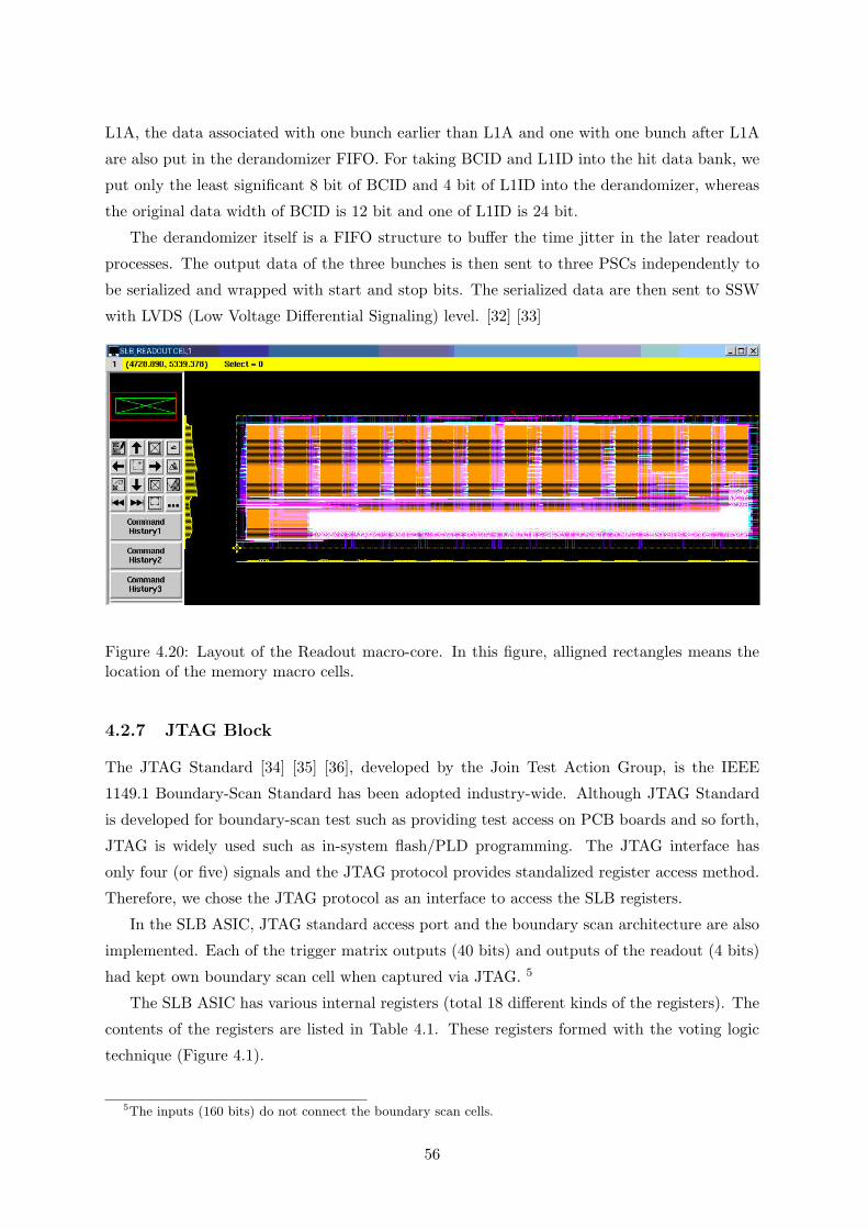
L1A, the data associated with one bunch earlier than L1A and one with one bunch after L1A
are also put in the derandomizer FIFO. For taking BCID and L1ID into the hit data bank, we
put only the least significant 8 bit of BCID and 4 bit of L1ID into the derandomizer, whereas
the original data width of BCID is 12 bit and one of L1ID is 24 bit.
The derandomizer itself is a FIFO structure to buffer the time jitter in the later readout
processes. The output data of the three bunches is then sent to three PSCs independently to
be serialized and wrapped with start and stop bits. The serialized data are then sent to SSW
with LVDS (Low Voltage Differential Signaling) level. [32] [33]
Figure 4.20: Layout of the Readout macro-core. In this figure, alligned rectangles means thelocation of the memory macro cells.
4.2.7 JTAG Block
The JTAG Standard [34] [35] [36], developed by the Join Test Action Group, is the IEEE
1149.1 Boundary-Scan Standard has been adopted industry-wide. Although JTAG Standard
is developed for boundary-scan test such as providing test access on PCB boards and so forth,
JTAG is widely used such as in-system flash/PLD programming. The JTAG interface has
only four (or five) signals and the JTAG protocol provides standalized register access method.
Therefore, we chose the JTAG protocol as an interface to access the SLB registers.
In the SLB ASIC, JTAG standard access port and the boundary scan architecture are also
implemented. Each of the trigger matrix outputs (40 bits) and outputs of the readout (4 bits)
had kept own boundary scan cell when captured via JTAG. 5
The SLB ASIC has various internal registers (total 18 different kinds of the registers). The
contents of the registers are listed in Table 4.1. These registers formed with the voting logic
technique (Figure 4.1).
5The inputs (160 bits) do not connect the boundary scan cells.
56

Table 4.1: Control Registers in SLB ASIC.
Name Bit RW DescriptionDEPTH 21 RW Depth of L1BufferTESTPULSE 5 RW Delay of Test pulse TriggerDELAY 4 RW No longer used (after version 3)DELAY A 4 RW Delay adjust for block A (form 0 to 3clk with 0.5clk)DELAY B 4 RW Delay adjust for block B (form 0 to 3clk with 0.5clk)DELAY C 4 RW Delay adjust for block C (form 0 to 3clk with 0.5clk)DELAY D 4 RW Delay adjust for block D (form 0 to 3clk with 0.5clk)SCHEME 1 RW Coincidence condition 0: 3 out of 4, 1:4 out of 4L1VETO 1 RW Level1 Accept (L1A) usage 0:Through,1:supress L1ACLKINV 1 RW Clock phase 0: Order, 1:InvertReset 1 RW Reset of Internal ECR and BCRDRDRST 1 RW Derandomizer ResetDCVETO 1 RW Input data Low Level 0:DC balanced, 1:NormalSEU 1 RO SEU flagMODULE 8 RO Module type and Module AddressOVERFLOW 8 RO Counts the number of Derandomizer Overflow was happened.ID 32 RO ID=0010 0100 0000 0100 1100 0000 0000 0100MASK1P 160 RW Mask Pattern for Readout and MatrixMASK1 160 RW Mask Enable for ReadoutMASK2P 160 RW Mask Pattern for Matrix onlyMASK2 160 RW Mask Enable for Matrix onlyTPP 160 RW Test Pulse Pattern
57

4.2.8 Implementation on the ASIC
The functions of the each block are described in Hardware Description Language (HDL). For
ASIC development, Verilog HDL is the default language we used.
At first, we verified the described function block has proper functionality using the Verilog
Simulator NC-Verilog (Cadence).
Then, the code is converted into gate-level code or net list using Logic Synthesizer Design-
Compiler (Synopsys). The gate-level code consists of instantiation of logic cells of the ASIC
libraries and the connection information among these logic cells. The gate-level code has equal
functionality with original code and can be implemented in the ASIC. At this point, we verified
the functionality using the gate-level code.
Finally, Place and Route (P&R) was performed. We used Milkyway and Apollo (Synopsys)
P&R software.
P&R consists of following steps:
1. Read in the gate-level code: The gates and connections are registered into the P&R
library.
2. Floor Plan: Define the areas for each function block will be located.
3. Gate Placement: The gates of the each function block will be placed automatically using
the algorithm that aims to minimize the total length of the circuit connections.
4. Routing: Place the connection wires among the gates. These connections are optimized
step-by-step. This step is very important to reduce the propagation delay.
5. Back Annotation: Extract actual delays between each connection. Extracted delay con-
sists of propagation delay and input port charge-up delays (= R × C). 6
4.2.9 Validation
We have tested an ASIC chip on test board to validate full functionality.
Figure 4.21 shows a schematic view of the inspection setup, which consists of a SLB ASIC
Test Board (equiped with a 256 pin QFP socket), 6 VME Pulse Pattern Generator (PPG)
modules for data feed, 2 FIFO modules for data Readout, a clock generator and so forth.
We prepared test vectors, which simulated the input patterns for the five types of SLB
ASIC (WD, WT, SD, ST, EI/FI) when muon tracks pass the TGCs. The input data from
PPG modules were fed to the DUT (Device Under Test) chip on the test board, and the
output are read out by FIFO modules in synchronous with 40.08 MHz system clock. The
output data are compared with test vector outputs. In this test, a universal clock generator
is used. TTC signals are provided via PPG (L1A, BCR, ECR), via a clock generator (CLK)
6Unfortunately some libraries (such as we used) do not have input port capacitance information.
58
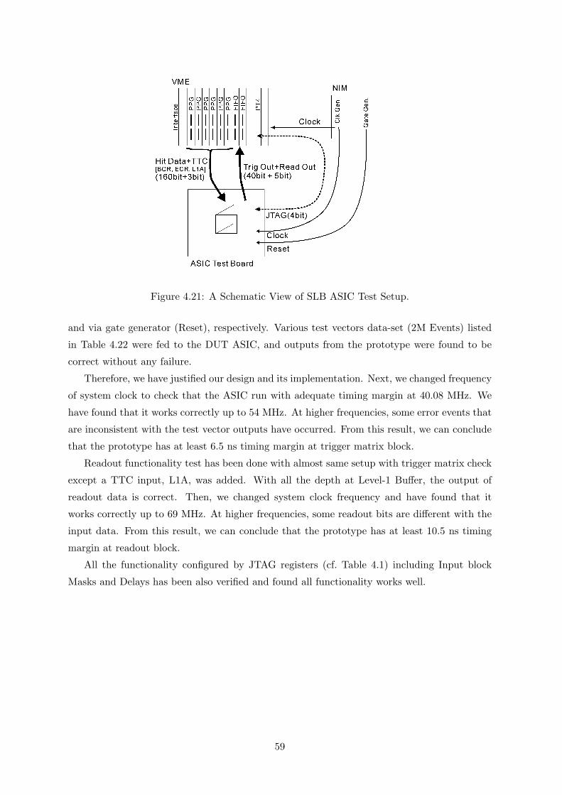
Figure 4.21: A Schematic View of SLB ASIC Test Setup.
and via gate generator (Reset), respectively. Various test vectors data-set (2M Events) listed
in Table 4.22 were fed to the DUT ASIC, and outputs from the prototype were found to be
correct without any failure.
Therefore, we have justified our design and its implementation. Next, we changed frequency
of system clock to check that the ASIC run with adequate timing margin at 40.08 MHz. We
have found that it works correctly up to 54 MHz. At higher frequencies, some error events that
are inconsistent with the test vector outputs have occurred. From this result, we can conclude
that the prototype has at least 6.5 ns timing margin at trigger matrix block.
Readout functionality test has been done with almost same setup with trigger matrix check
except a TTC input, L1A, was added. With all the depth at Level-1 Buffer, the output of
readout data is correct. Then, we changed system clock frequency and have found that it
works correctly up to 69 MHz. At higher frequencies, some readout bits are different with the
input data. From this result, we can conclude that the prototype has at least 10.5 ns timing
margin at readout block.
All the functionality configured by JTAG registers (cf. Table 4.1) including Input block
Masks and Delays has been also verified and found all functionality works well.
59

Figure 4.22: Various SLB Test Vectors and Results.
Trigger Type Tracks/event Scheme # of Error3 out of 4 04 out of 4 03 out of 4 04 out of 4 03 out of 4 04 out of 4 03 out of 4 04 out of 4 03 out of 4 04 out of 4 03 out of 4 04 out of 4 02 out of 3 03 out of 3 02 out of 3 03 out of 3 02 out of 3 03 out of 3 01 out of 2 02 out of 2 01 out of 2 02 out of 2 01 out of 2 02 out of 2 01 out of 2 02 out of 2 01 out of 2 02 out of 2 01 out of 2 02 out of 2 0
EI/FI
1track
2tracks
3tracks
Strip Triplet(ST)
1track
2tracks
3tracks
Wire Triplet(WT)
1track
2tracks
3tracks
Sire Doublet(SD)
1track
2tracks
3tracks
1track
2tracks
3tracks
Wire Doublet(WD)
60

4.3 Sector Logic
The Sector Logic is the final part of ATLAS TGC muon Trigger system. One Sector Logic
covers one trigger sector (shown in Figure 3.4 in Section 3.3.). In each 25 ns bunch crossing, the
Sector Logic receives track information of wires (∆R) and strips (∆φ) from High-pT modules.
To get transverse momentum (pT) of muon tracks, the Sector Logic combines both inputs.
Then, it chooses the two highest-pT tracks in each trigger sector. Resulting trigger information
including pT and RoI location are sent to the MUCTPI.
4.3.1 Overview
Requirements for the track selection in the Sector Logic are:
1. Both transverse momentum and hit position on the pivot plane of the TGC should be
reconstructed from hit information of wires and strips from the High-pT modules.
2. Information of the innermost TGCs (EI/FI stations) should be used for track finding to
suppress fake tracks and low momentum background tracks.
3. Muons with more than 6 GeV/c pT from the interaction point should be accepted.
4. Accepted muon tracks should be classified into six groups based on pT information. These
6 pT thresholds should be programmable.
5. Up to 2 highest-pT tracks are chosen in each trigger sector. These track information
including pT and RoI location should be sent to the MUCTPI.
6. Track finding should be applied to each beam crossing. (i.e. These circuitry are imple-
mented with dead time less logic)
The Sector Logic is also equipped with a Level-1 Readout Buffer. The High-pT module
outputs and the Sector Logic output thus are included in the Readout data flow in the same
way as the chamber data. This information from the Sector Logic will play important role in
diagnosis of the trigger system as well as in checking trigger performance.
4.3.2 Design of the Sector Logic
A schematic of the Sector Logic is shown in Figure 4.23. The Sector Logic consists of Decoder,
R-φ coincidence matrices, Track Selection logic and Encoder. The logic operates in pipeline
mode at 40.08 MHz.
The Sector Logic receives hit information of wires and strips from each High-pT module in
one trigger sector (cf. Figure 3.4 in Section 3.3). In order to get transverse momentum of tracks,
it combines both inputs and then classifies muon tracks into six levels (R-φ Coincidence).
61
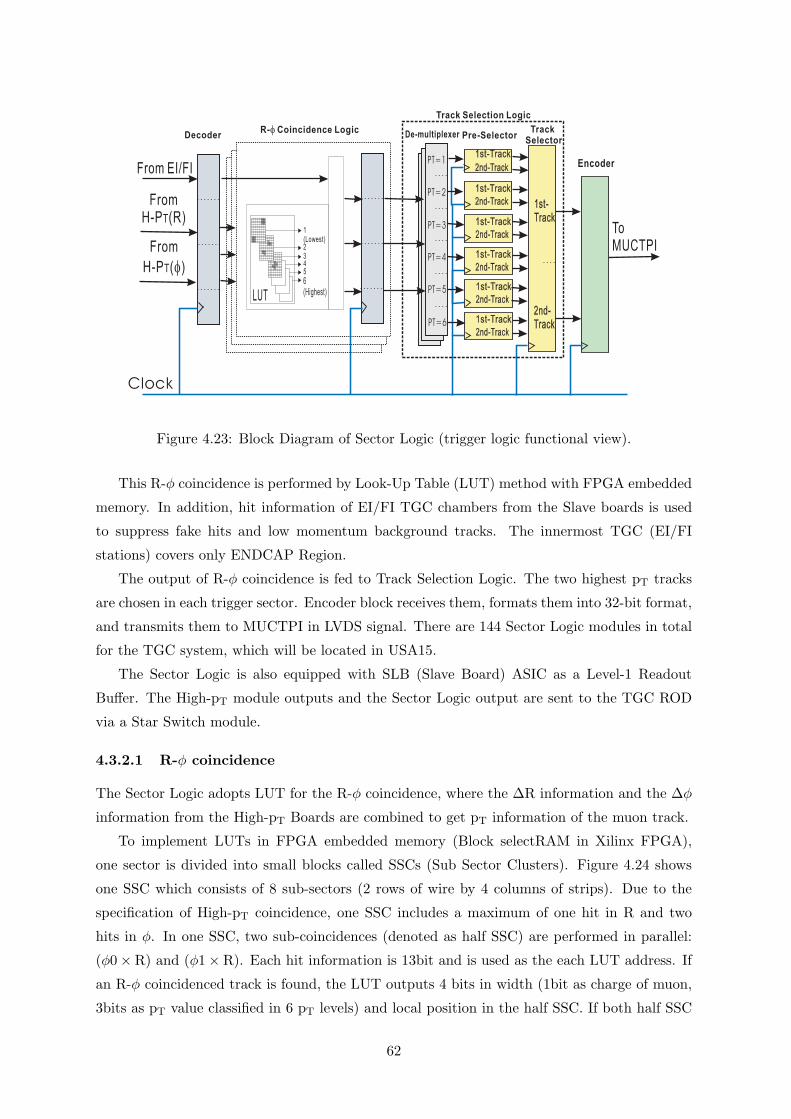
From EI/FI
1(Lowest)
LUT
45
6(Highest)
23
FromH-P (R)T
From
H-P ( )T f
DecoderR- Coincidence Logicf
De-multiplexer
1st-Track
2nd-Track
1st-Track
2nd-Track
1st-Track
2nd-Track
1st-Track
2nd-Track
1st-Track
2nd-Track
1st-Track
2nd-Track
1st-Track
2nd-Track
PT=1
PT=2
PT=3
PT=4
PT=5
PT=6
Pre-SelectorTrack
Selector
Encoder
ToMUCTPI
Clock
Track Selection Logic
Figure 4.23: Block Diagram of Sector Logic (trigger logic functional view).
This R-φ coincidence is performed by Look-Up Table (LUT) method with FPGA embedded
memory. In addition, hit information of EI/FI TGC chambers from the Slave boards is used
to suppress fake hits and low momentum background tracks. The innermost TGC (EI/FI
stations) covers only ENDCAP Region.
The output of R-φ coincidence is fed to Track Selection Logic. The two highest pT tracks
are chosen in each trigger sector. Encoder block receives them, formats them into 32-bit format,
and transmits them to MUCTPI in LVDS signal. There are 144 Sector Logic modules in total
for the TGC system, which will be located in USA15.
The Sector Logic is also equipped with SLB (Slave Board) ASIC as a Level-1 Readout
Buffer. The High-pT module outputs and the Sector Logic output are sent to the TGC ROD
via a Star Switch module.
4.3.2.1 R-φ coincidence
The Sector Logic adopts LUT for the R-φ coincidence, where the ∆R information and the ∆φ
information from the High-pT Boards are combined to get pT information of the muon track.
To implement LUTs in FPGA embedded memory (Block selectRAM in Xilinx FPGA),
one sector is divided into small blocks called SSCs (Sub Sector Clusters). Figure 4.24 shows
one SSC which consists of 8 sub-sectors (2 rows of wire by 4 columns of strips). Due to the
specification of High-pT coincidence, one SSC includes a maximum of one hit in R and two
hits in φ. In one SSC, two sub-coincidences (denoted as half SSC) are performed in parallel:
(φ0 × R) and (φ1 × R). Each hit information is 13bit and is used as the each LUT address. If
an R-φ coincidenced track is found, the LUT outputs 4 bits in width (1bit as charge of muon,
3bits as pT value classified in 6 pT levels) and local position in the half SSC. If both half SSC
62

Figure 4.24: Detail of Sub Sector Cluster (SSC) for the R-φ coincidence togher with hit inputs.
has candidates, higher pT level candidate is chosen as the SSC output. In case both candidates
has same pT level, the candidate in the lower-φ half SSC is chosen. Finally, the track position
information of the sector (RoI) is added.
Each ENDCAP trigger sector covers 37 rows of wire by 4 columns of strips. To cover
this, 19 SSCs are needed. However, SSCs on chamber boundaries should be treated as two
different SSC from the viewpoint of the R-φ coincidence. Therefore, 23 SSCs are needed in one
ENDCAP trigger sector.
4.3.2.2 Track Selection Logic (Pre-Track Selector, Track Selector)
Track Selection logic block consists of 6 pre-track selectors, and a track selector. Figure 4.25
shows schematics of Track selection logic block.
Track candidates from R-φ Coincidence are sent to the Pre-Track Selectors. Each Pre-Track
Selector unit collects tracks with the same pT level and selects 2 tracks with the 1st and 2nd
lower (higher R). There are 6 identical Pre-Track selector units corresponding to 6 levels of
track pT. The output from the Pre-Track selector includes position information of triggered
sub-sector.
The Track Selector unit picks up the final 2 highest-pT tracks among 12 tracks from 6 Pre-
Track Selectors. The output from the Track Selector is a combination of position information
(RoI number), charge sign of track, and 6 levels of pT information.
4.3.2.3 Decoder
Each High-pT ASIC chip chooses up to two hits and outputs them in 20 bit format. The High-
pT ASIC can be configured for wire or strip by setting configuration pin. Figure 4.26 shows
each High-pT ASIC outputs.
Figure 4.27 shows the connection between wire High-pT Boards and Sector Logic. As shown
in this Figure, four High-pT ASICs cover in an ENDCAP trigger sector and two High-pT ASICs
63

PT=6
PT=5
PT=4
PT=3
PT=2
PT=1
Pre-Track Selector Track Selector
Figure 4.25: A schematic of Track Selection logic block.
Figure 4.26: Data Format from Hi-pT ASIC chip (Wire mode).
64

cover in an ENDCAP trigger sector. The signal format between High-pT Boards and a Sector
Logic Board is defined in “HPT Board g-link connection table” [17].
1 �¨1 hit
6 �¨2 hit
6 �¨2 hit
6 �¨2 hitEW0
F0
M3
TGC Doublet(Pivot plane)
Interaction Point
h = 1.92
h = 2.29
h = 1.62
h = 1.37
h = 1.05
}
}}}}}
FORWARD
High-P module(Wire)
T
ENDCAP
FORWARD
ENDCAP
{{{
6 �¨2 hit
2 �¨2 hit {
TriggerSector(Subsector)
{
SSC0
SSC1
SSC2
SSC3
SSC4
SSC5
SSC6
SSC7
SSC8
SSC9
SSC10
SSC11
SSC12
SSC13
SSC14
SSC15
SSC16
SSC17
SSC18
SSC0
SSC1
SSC2
SSC3
SSC4
SSC5
SSC6
SSC7
0
1
2
3
0
1
2
FORWARD
ENDCAP
Figure 4.27: Wire High-pT Boards coverage and its correspondant SSCs.
65

*Wire (R) Signal: Wire (R) hit signal consists of ∆R information with a sign bit(∆R: 1+4
bits), a bit for discriminating between Low-pT coincidence and High-pT coincidence
(H/L), position information of R (HitID+POS: 3+1 bits).
H/L
POSHitID DR
2nd Hit
H/L
POSHitID DR
1st Hit
�} �}
Figure 4.28: Wire (R) input signal from from Wire High-pT Board.
ENDCAP Region: Wire signals for ENDCAP Region sector are covered by four High-
pT ASICs. In Decoder block in ENDCAP Region Sector Logic, SSC# (Sub Sector
Cluster Number) are generated from HitID as:
High-pT ASIC SSC#EW0-Chip0 SSC# = HitIDEW0-Chip1 SSC# = HitID + 1EW0-Chip2 SSC# = HitID + 7EW0-Chip3 SSC# = HitID + 13
The following table shows correspondances each High-pT ASIC, its cover region and
SSC#.
High-pT ASIC η SLB ASIC SSC# HitID Max HitEW0-Chip0 -1.05 EWD0 EWT0 0 0 1 → 1EW0-Chip1 1.05-1.37 EWD1 EWT1 1 2 0 1 6 → 2
EWD2 3 4 2 3EWD3 EWT2 5 6 4 5
EW0-Chip2 1.37-1.62 EWD4 EWT3 7 8 0 1 6 → 2EWD5 9 10 2 3EWD6 EWT4 11 12 4 5
EW0-Chip3 1.62-1.92 EWD7 EWT5 13 14 0 1 6 → 2EWD8 15 16 2 3EWD9 EWT6 17 18 4 5
66

FORWARD Region: Wire signals for FORWARD Region sector are covered by two
High-pT ASICs. In Decoder block in FORWARD Region Sector Logic, SSC# (Sub
Sector Cluster Number) are generated from HitID as:
High-pT ASIC SSC#FW0-Chip0 SSC# = HitIDFW0-Chip1 SSC# = HitID + 6
The following table shows correspondances each High-pT ASIC, its cover region and
SSC#.
High-pT ASIC η SLB ASIC SSC# HitID Max HitFW0-Chip0 1.92-2.29 FWD0 FWT0 0 1 0 1 6 → 2
FWD1 2 3 2 3FWD2 FWT1 4 5 4 5
FW0-Chip1 2.29- FWD3 FWT2 6 7 0 1 2 → 2
*Strip (φ) Signal: Strip (φ) hit signal consists of ∆φ information whith a sign bit (∆φ:
1+3 bits), a bit for discriminating between Low-pT coincidence and High-pT coincidence
(H/L), position information of φ (HitID+POS: 3+1 bits). Unused 4th bit of ∆φ infor-
mation is set to “0”.
H/L
POSHitID Df
2nd Hit
H/L
POSHitID Df
1st Hit
�} �}0 0
Figure 4.29: Strip (φ) input signal from from Strip High-pT Board.
ENDCAP Region: Strip signals for ENDCAP Region sector are covered by two High-
pT ASICs. In Decoder block in ENDCAP Region Sector Logic, TGC (Pivot Cham-
ber) ID and hit position in φ are calculated from HitID and POS as:
67
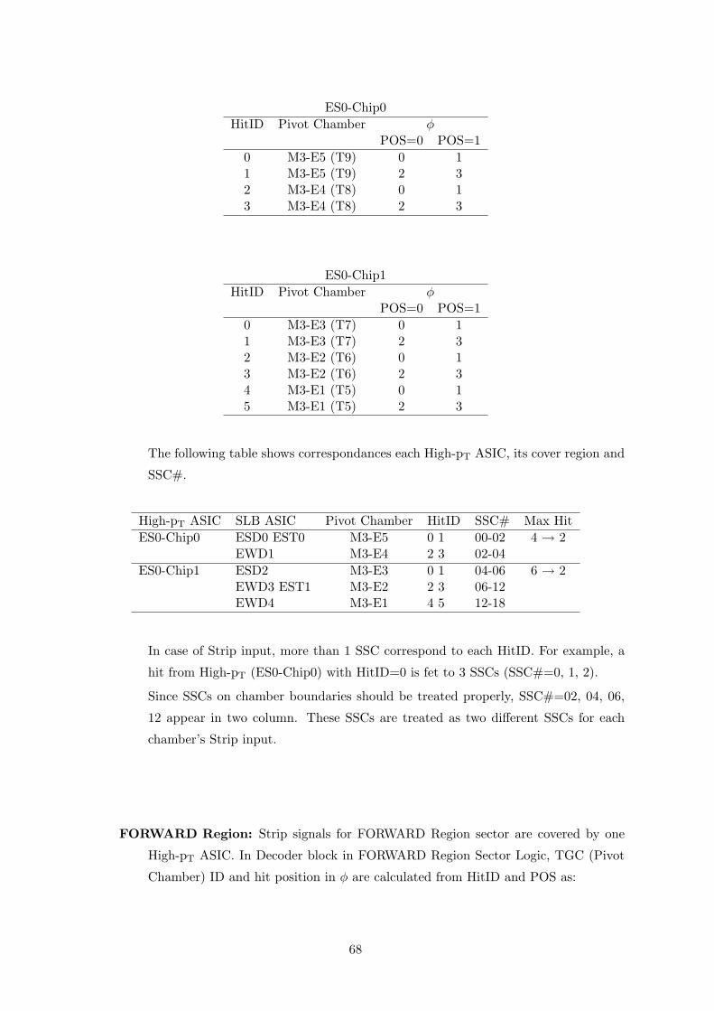
ES0-Chip0HitID Pivot Chamber φ
POS=0 POS=10 M3-E5 (T9) 0 11 M3-E5 (T9) 2 32 M3-E4 (T8) 0 13 M3-E4 (T8) 2 3
ES0-Chip1HitID Pivot Chamber φ
POS=0 POS=10 M3-E3 (T7) 0 11 M3-E3 (T7) 2 32 M3-E2 (T6) 0 13 M3-E2 (T6) 2 34 M3-E1 (T5) 0 15 M3-E1 (T5) 2 3
The following table shows correspondances each High-pT ASIC, its cover region and
SSC#.
High-pT ASIC SLB ASIC Pivot Chamber HitID SSC# Max HitES0-Chip0 ESD0 EST0 M3-E5 0 1 00-02 4 → 2
EWD1 M3-E4 2 3 02-04ES0-Chip1 ESD2 M3-E3 0 1 04-06 6 → 2
EWD3 EST1 M3-E2 2 3 06-12EWD4 M3-E1 4 5 12-18
In case of Strip input, more than 1 SSC correspond to each HitID. For example, a
hit from High-pT (ES0-Chip0) with HitID=0 is fet to 3 SSCs (SSC#=0, 1, 2).
Since SSCs on chamber boundaries should be treated properly, SSC#=02, 04, 06,
12 appear in two column. These SSCs are treated as two different SSCs for each
chamber’s Strip input.
FORWARD Region: Strip signals for FORWARD Region sector are covered by one
High-pT ASIC. In Decoder block in FORWARD Region Sector Logic, TGC (Pivot
Chamber) ID and hit position in φ are calculated from HitID and POS as:
68

FS0-Chip2HitID Pivot Chamber φ
POS=0 POS=10 M3-F (T2) 0 11 M3-F (T2) 2 3
The following table shows correspondances each High-pT ASIC, its cover region and
SSC#.
High-pT ASIC SLB ASIC Pivot Chamber HitID SSC# Max HitFS0-Chip2 FSD0 FST0 M3-F 0 1 00-15 2 → 2
In case of FORWARD region Strip input, these inputs are fed to all SSCs. Since
there is only one chamber in FORWARD Region, special treatment for chamber
overlap isn’t required.
4.3.2.4 Encoder
The Encoder block of the Sector Logic sends resulting trigger information of 2 highest-pT tracks
in the Sector to feed it to the MUCTPI.
TGC Sector Logic formats its output in 32-bit format, and transmits them to MUCTPI in
LVDS signal. The format is shown in Table 4.2.
69

Table 4.2: Data format between Sector Logic and MUCTPI [16].
Bit# Meaning ENDCAP FORWARD0 > 2 candidates in the sector1 ROI1 with overlap flags ROI1[0] ROI1[0]2 ROI1[1] ROI1[1]3 ROI1[2] ROI1[2]4 ROI1[3] ROI1[3]5 ROI1[4] ROI1[4]6 ROI1[5] ROI1[5]7 ROI1[6] res8 ROI1[7] res9 OVL1 (Note1) res10 ROI2 with overlap flags ROI2[0] ROI2[0]11 ROI2[1] ROI2[1]12 ROI2[2] ROI2[2]13 ROI2[3] ROI2[3]14 ROI2[4] ROI2[4]15 ROI2[5] ROI2[5]16 ROI2[6] res17 ROI2[7] res18 OVL2 (Note1) res19 pT1[0] (Note2)20 pT1[1]21 pT1[2]22 pT2[0] (Note2)23 pT2[1]24 pT2[2]25 > 1 candidate in ROI1 (Note3) res res26 > 1 candidate in ROI2 (Note3) res res27 BCID[0] (Note4)28 BCID[1]29 BCID[2]30 Candidate1 sign (Note5)31 Candidate2 sign (Note5)
70

Note1. OVLi[1..0]
00: No overlap
01: Overlap in φ
10: Overlap in η
11: Overlap in φ and η
Note2. pTi[2..0]
000: Low pT 1 (Lowest pT)
001: Low pT 2
010: Low pT 3
011: High pT 1
100: High pT 2
101: High pT 3 (Highest pT)
111: No Candidate
000: Reserved
Note3. This bit field is for Barrel Muon Trigger system (RPC) only. TGC Electronics cannot
tell >1 candidate in a RoI.
Note4. Three bits for the BCID should be enough for checking purpose as it is very unlikely
to have a misalignment greater than 8 BC. They are the low order bits of the BCID
provided by the TTC system (TTCrx receiver chips or equivalent).
Note5. Candidate sign
0: Negative (µ−)
1: Positive (µ+)
The double counting in the ENDCAP-FORWARD overlap region can be removed by cutting
the edge of strips of the pivot chambers in the FORWARD Region, so as not to make a
coincidence in φ projection. Therefore, the MUCTPI does not need to take care and there is
no overlap bit in the output for the FORWARD Region Sector Logic.
The MUCTPI receives TGC Sector Logic outputs and RPC Sector Logic outputs. It solves
overlap problem between TGC and RPC, mentioned in Section 2.1.1, and then calculates overall
multiplicities of muon tracks for six muon threthold levels.
The latest interface definition including Table 4.2 and strategy for solving the overlap
problem are described in the official document; “Interface & overlaps in the LVL1 muon trigger
system” [16].
71
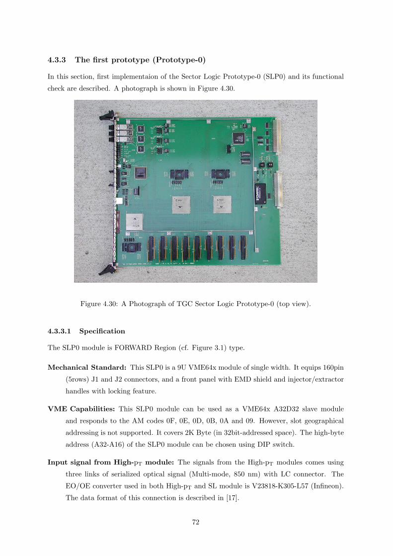
4.3.3 The first prototype (Prototype-0)
In this section, first implementaion of the Sector Logic Prototype-0 (SLP0) and its functional
check are described. A photograph is shown in Figure 4.30.
Figure 4.30: A Photograph of TGC Sector Logic Prototype-0 (top view).
4.3.3.1 Specification
The SLP0 module is FORWARD Region (cf. Figure 3.1) type.
Mechanical Standard: This SLP0 is a 9U VME64x module of single width. It equips 160pin
(5rows) J1 and J2 connectors, and a front panel with EMD shield and injector/extractor
handles with locking feature.
VME Capabilities: This SLP0 module can be used as a VME64x A32D32 slave module
and responds to the AM codes 0F, 0E, 0D, 0B, 0A and 09. However, slot geographical
addressing is not supported. It covers 2K Byte (in 32bit-addressed space). The high-byte
address (A32-A16) of the SLP0 module can be chosen using DIP switch.
Input signal from High-pT module: The signals from the High-pT modules comes using
three links of serialized optical signal (Multi-mode, 850 nm) with LC connector. The
EO/OE converter used in both High-pT and SL module is V23818-K305-L57 (Infineon).
The data format of this connection is described in [17].
72

Output signals for MUCTPI: The signals transmits to the MUCTPI are 32-bit format
LVDS signals. A 68-pin half pitch connector (8931E-068-178L (KEL)) is equipped.
Input signal for TTC distributor: The signal level for TTC is LVDS. The SLP0 inputs 4
TTC signals (BC (Des1), BCR, ECR, L1A) from TTC distributor with a 20-pin flat cable
connector.
Input and Output signals for Readout: A SLB ASIC is mounted for Readout of input
and output signals of the Sector Logic. The trigger matrix feature of SLB ASIC is
disabled. The Readout output signals are converted into serialized LVDS signal with
LVDS serializer (DS92LV1023TMSA). A RJ-45 connector is equipped for the cable to
Star Switch (SSW).
4.3.3.2 Implementaion
The core function blocks of the Sector Logic are divided two stages and each stage is imple-
mented in the FPGA device(s) respectively. The block diagram is shown in Figure 4.31.
Optical
Interface
3links
(50bit)
OE
Deserialize
Decoder
Dispatch
each SSCs
R-
Coincidence
f
Classify hits
into 6 pT levels
19x8SSCs
X8
Pre
Track Selector
Choose 2 hits in
each pT level
Final
Selector
Choose 2 hits
in a Sector
16x6pTs
Encoder
Encode2 hits
FPGA0(SSC0-SSC5), FPGA1(SSC6-SSC7)
FPGA2
8X8SSCs
32bit
X6
17
17
16
Figure 4.31: Block Diagram of Sector Logic Prototype-0 (FORWARD Region type).
At first stage, decoder block and R-φ Coincidence block are implemented. The decoder
block inputs the R- and φ- High-pT outputs and rearrange them into each SSC inputs. The
R-φ Coincidence block uses FPGA embedded memory (Block SelectRAM) as LUT memory
for each SSCs. In order to implement R-φ Coincidence, we choose extended memory type of
73
the Xilinx Virtex-E EM series FPGA [37] (XCV405E (Block SelectRAM bits: 560KByte)).
FPGA0 covers from SSC0 to SSC5 and FPGA1 covers SSC6 and SSC7.
At second stage, Track Selection Logic (Pre-Track Selector and Track Selector) and Encoder
are implemented. The Encoder receives two track candidates from the Track Selection Logic
and formats them into for MUCTPI output format [16]. This block is implemented in one
Xilinx Virtex-E FPGA [37] (XCV400E) named as FPGA2.
4.3.3.3 Validation
First, we have tested the Prototype-0 board to validate the Sector Logic design. We prepared
test vectors, which simulated the input patterns for the Sector Logic when muon tracks pass the
TGCs. Series of input data were fed to the prototype through an optical interface module with
the serializer (G-Link), which was specially made for this test. The output to the MUCTPI
was read out. The input and the output were synchronized to 40.08 MHz system clock. In
this test, a universal clock generator was used. The latency from the G-Link input to the
trigger output was found to be 6 clocks as expected from the design. The prototype was tested
for over 1M events and outputs were found to be correct without any failure. Therefore, we
have justified our design and its implementation for the prototype. Next, we changed system
clock frequency to check that the prototype board runs with adequate timing margin at 40.08
MHz. We have found that it worked correctly up to 51.5 MHz. At higher frequencies, we
have found problems on the links between receivers on the prototype and transmitters on the
optical serializer module. From this result, we can conclude that the prototype has at least 5.5
ns timing margin.
4.3.3.4 Integration test with the MUCTPI
As explained in section 4.3.2.4, the link between the Sector Logic and the MUCTPI employs
32-bit width LVDS. Timing alignment issues and data integrity through the link were tested to
check the trigger data transmission from the Sector Logic to the MUCTPI. The FPGA design
of the Sector Logic Prototype-0 was once configured so that test pattern data words loaded in
registers were sent to the MUCTPI. The encoder and driver parts of the FPGA design were
un-changed from the original design. There was no bit error occurred during 109 events trigger
data transmission. Details of these tests are reported in [19].
4.3.3.5 Test beam at H8 beam line in CERN
We have tested whole TGC electronics system with MUCTPI and CTP using muon beam at H8
experimental area of CERN SPS in 2003 [30], [31]. Configuration of TGC electronics system is
same as a part of forward region and we used Prototype-0 as a Sector Logic for Forward region.
Whole system worked well and the Sector Logic successfully issued trigger words to MUCTPI.
We checked consistency between trigger data in SLB ASIC on the Sector Logic through the
74

TGC ROD and data received by MUCTPI through the MIROD. Figure 4.32 shows correlation
plots of pT levels and ROI location. We observed 0.2% inconsistencies out of about 2M events.
But no errors were found in the Sector Logic functionalities and it might be caused by timing
synchronization in the readout path.
Figure 4.32: Correlation plots of pT levels (left) and ROI location(right) for trigger words readout by Sector Logic vs MUCTPI.
4.3.4 Final Design of whole Sector Logic system
As described in the previous section, the design and its functionality of the TGC Sector Logic
have been verified using its prototype (SLP0).
Then, we began to design entire TGC Sector Logic system. In this section, the Sector Logic
system and each component are described.
Figure 4.33 shows whole TGC Sector Logic system. The TGC Sector Logic system consists
of following components:
1. FORWARD Sector Logic: 48 Sectors/System (24 Sectors/Side)
In final design, two Sector Logics are implemented in a FORWARD Sector Logic board.
Therefore, there are 24 FORWARD Sector Logic boards in the System and they are stored
in two 9Ux400mm VME64x crates.
2. ENDCAP Sector Logic: 96 Sectors/System (48 Sectors/Side)
The ENDCAP Sector Logic also implements two Sector Logics in a board. Therefore,
there are 48 ENDCAP Sector Logic boards in the System and they are stored in four
9Ux400mm VME64x crates.
3. TTC Fanout:
For Sector Logic, the following signals are distributed: Clock, BCR (Bunch ID Clear),
75

FORWARD
High-pT Boards
ENDCAP
High-pT Boards
FORWARD
Sector Logic Boards
ENDCAP
Sector Logic Boards
R, f
R, f
EI/FI PS-Boards
VME 9Ux400mm
VME 9Ux400mm
g-link (optical link)
g-link (optical link)
EI/FI Optical
Fanout modules
HSC Crate
HSC module
SL Crate
SL Crate
SSW modules
R, hitf
R, hitf
Readout Data
(LVDS)
Readout Data
(LVDS)
TTC Fanout
(Service Patch Panel)
TTC Signals
(to All SLs)
g-link (optical link)
g-link
(optical link)
Figure 4.33: The Sector Logic system.76

ECR (Event ID Clear), L1A (Level-1 Trigger Accept) and Reset. The Service Patch-
Panel for PS-Boards can be used for the Sector Logic TTC Fanout by setting on-board
jumper pin.
4. EI/FI Optical Fanout module: 96 Optical links/System (48 optical links/Side)
Hit signals from EI/FI PS-Boards are should be distributed to appropriate ENDCAP
Sector Logic boards (up to four boards). We designed six channels 1:4 Fanout Optical
Fanout Modules, which can be stored in HSC crate (without VME access). There are
total 8 Optical Fanout modules in the system.
5. SSW Module:
A SSW Module equips 10 inputs. One TGC Side can be covered 4 SSW modules (12
FORWARD Sector Logic boards and 24 ENDCAP Sector Logic boards). The output
from the SSW module is sent to the ROD module.
6. HSC Crate and HSC module: 2 Crates/System (1 Crate/Side)
A HSC Crate covers one TGC Side and stores 4 EI/FI Optical Fanout modules, 4 SSW
modules and a HSC module.
4.3.4.1 Final Design of Sector Logic board
In this section, the specification of the final design Sector Logic board is described.
The final design is developed with latest FPGA devices at the design time, this gives
following merits:
• Three FPGAs in SLP0 is integrated in one FPGA.
• Two Sector Logics are implemented in one board. (i.e. One board covers two trigger
sector.)
• In addition the final design Sector Logic board has more timing margins and its cost is
cheaper than the SLP0 since FPGA has been improved very much in these years.
Main FPGA: We chose Xilinx Virtex-II FPGA [37] for Sector Logic implementation. The
Virtex-II FPGA has 18 Kbit Block SelectRAMs in the device. 4 Block SelectRAM is
required to implement a LUT for one SSC.
• FORWARD Sector Logic:
There are 8 SSCs in FORWARD Sector and requires 8 × 4=32 Block SelectRAMs.
We selected XC2V1000, which have 40 Block SelectRAMs.
• ENDCAP Sector Logic:
There are 23 SSCs in ENDCAP Sector and requires 23 × 4=92 Block SelectRAMs.
We selected XC2V3000, which have 96 Block SelectRAMs.
77

VME Control CPLD: For VME control and interface, we chose Xilinx CoolRunner-II CPLD,
XC2S256-PQ208C. This CPLD provides following features: VME access, FPGA program-
ming from VME, EPROM writing by JTAG protocol and JTAG controller.
Input signal from high-pT modules and EI/FI Optical Fanout module: These signals
are serialized optical signal (Multi-mode, 850 nm with LC connector.
• FORWARD Sector Logic:
The signals received from the High-pT modules are 3 links times 2 sector. 6 EO/OE
converters (V23818-K305-L57,Infineon) are used. We selected XC2V1000, which
have 40 Block SelectRAMs.
• ENDCAP Sector Logic:
The signals received from the High-pT modules are 6 links times 2 sector. The signals
received from the EI/FI Optical fanout are 4 links. Dual Receiver (M2R-25-4-1-TL,
STRATOS Lightwave) is used to reduce the number of optical converters. 6 (for
High-pT modules)+2(for EI/FI) OE/OE converter (Dual Receiver) is used.
Output signals for MUCTPI: The signals transmits to the MUCTPI are 32-bit format
LVDS signals. The ANSI/SFF-8441 standard 68-pin VHDCI type connectors for each
Sector are equipped. Detailed information is described in [16].
Input signal for TTC distributor: The signal level for TTC is LVDS. The SLP0 inputs 5
TTC signals (BC(Des1), BCR, ECR, L1A and Reset) from TTC distributor with a 10-pin
flat cable connector.
Input and Output signals for Readout: Two SLB ASICs are mounted for input and out-
put signals of each Sector Logic Readout. The trigger matrix feature is disabled. The
Readout output signals are converted into serialized LVDS signal with LVDS serializer
(DS92LV1023TMSA). A JRC (JTAG Routing Circuit, which is used on PS-Board) is also
mounted to select both SLB’s JTAG path. A RJ-45 connector is equipped to send the
serialized data to Star Switch (SSW). The channel assignment is same with PS-Boards.
G-Link Monitor: For monitoring G-Link status, we chose a Xilinx Spartan-IIE FPGA (XC2S50E-
PQ208C). This FPGA provides G-Link status registers which can be accessed via VME
and “G-Link OK” signals for each Main FPGA.
Figure 4.34 and Figure 4.35 show the layouts for FORWARD Sector Logic and ENDCAP
Sector Logic respectively.
78
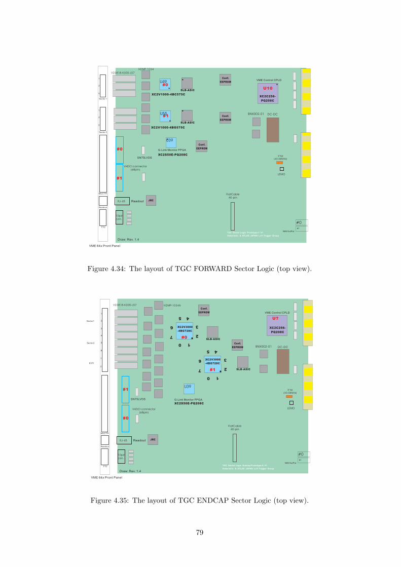
V23818-K305-L57
HDMP-1034
BNX002-01
VHDCI connector
(68pin)
U10
1
2
3
VME 64x Pront Panel
TGC Sector Logic Prototype-1 V1
Kobe Univ. & ATLAS JAPAN Lvl1 Trigger Group
XC2V1000-4BG575C
1
2
3
#0
#1
#0
#1
Conf.
EEPROM
RJ-45
10pin
con.
Readout
SLB-ASIC
XC2V1000-4BC575C
SLB-ASIC
Conf.
EEPROM
Sector 1
Sector 2
MUCTPI
Readout
TTC
JRC
Draw: Rev. 1.4
DC-DC
Conf.
EEPROM
U39
U55
U49
SN75LVDS
#0
#1
NIM OutPut
XC2S50E-PQ208C
XC2C256-
PQ208C
FlatCable
40-pin
G-Link Monitor FPGA
VME Control CPLD
LEMO
X’tal
(40.08MHz)
Figure 4.34: The layout of TGC FORWARD Sector Logic (top view).
V23818-K305-L57 HDMP-1034A
BNX002-01
VHDCI connector
(68pin)
LEMO
X’tal
(40.08MHz)
DC-DC
U?
10
2
3
45
6
7
VME 64x Pront Panel
TGC Sector Logic Endcap Prototype-0 V1
Kobe Univ. & ATLAS JAPAN Lvl1 Trigger Group
10
2
3
45
6
7
#0
#0
#1
FlatCable
40-pin
XC2V3000
-4BG728C
XC2V3000
-4BG728C
#1
Conf.
EEPROM
Conf.
EEPROM
SLB-ASIC
SLB-ASIC
1
2
3
4
5
6
Sector1
2
EI/FI
Draw: Rev. 1.4
U39
#0
#1
NIM OutPut
Sector2
1
XC2C256-
PQ208C
XC2S50E-PQ208C
RJ-45
10pin
con.
Readout
Readout
TTC
JRC
MUCTPI
SN75LVDS
VME Control CPLD
G-Link Monitor FPGA
Figure 4.35: The layout of TGC ENDCAP Sector Logic (top view).
79
4.4 Radiation Tolerance
As discussed in Section 4.1, four types of ASICs are extensively used in the on-detector part of
the ATLAS Level-1 muon Endcap trigger system. (See Figure 4.2 on page 42.) Anti-Fuse type
FPGAs are also used for other components with not a large number of same chip is used. As
illustrated on Figure 3.3 on page 37, the ASICs and FPGAs are mounted on boards, which are
just behind or outer rims of the TGC wheels.
The region where these electronics (except ASD board location) are mounted will be exposed
to the radiation of up to ∼210 Gy (including a safety factor 70) and a energetic hadron (>20
MeV) integrated intensity of up to ∼ 2.1 × 10¹⁰ hadrons/cm2 for ten years in the normal
operation [12] [14]. All ASICs we made except ASD ASIC 7 and both Anti-Fuse type FPGAs
are fabricated in the CMOS process. CMOS process is not sensitive to neutrons in estimated
level (up to ∼ 1.2×10¹² 1MeV eq. neutrons/cm2, including a safety factor 20) in the on-detector
TGC electronics system.
We must clarify all the devices (of ASICs, FPGAs and other Commercial-Off-The-Shelf (COTS))
to survive in this radiation environment with no degradation in performance in terms of total
ionizing dose (TID) and single event effects (SEE).
We intend to use four technologies for the chip production; (1) 0.35 µm standard full custom
CMOS of ROHM, (2) 0.35 µm Gate Array CMOS of Hitachi for ASIC productions and (3-4)
two Actel Anti-Fuse type FPGAs [38].
In order to validate the devices made with these technologies are applicable in the on-
detector TGC electronics system, we have made the irradiation measurements of them using
γ-ray from 60Co for TID and 70 MeV proton beam for SEE.
In this Section, the results of the irradiation tests for chips fabricated with technologies
listed above are described. The result of the irradiation test for other COTS are documented
in [22].
4.4.1 Test for Total Ionization Dose (TID)
4.4.1.1 TID Test Procedure
The γ-ray irradiation facility is two-story structure; an irradiation room on the downstairs and
a store with a lead container for the irradiation sources on the upstairs. 48 pencil type rods as
radiation sources are filled in a cylindrical vessel, which moves between the upstairs and the
downstairs via remote control system. (Figure 4.36 shows the experiment setup.)
The maximum strength of the sources and the maximum dose rate are 22 TBq and 1000 Gy/hr
in H2O. The irradiation rate can be controlled by changing the radiation source and the lo-
cation of the DUT (we call hereafter a target chip as DUT; Device Under Test). We used
7The study of radiation tolerance including neutron irradiation for ASD ASIC had been done [23] [24], hencethe ASD ASIC issue does not described in this thesis.
80
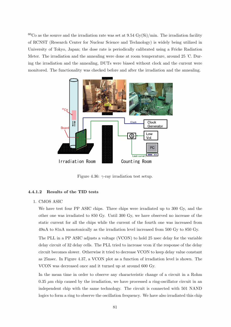
60Co as the source and the irradiation rate was set at 9.54 Gy(Si)/min. The irradiation facility
of RCNST (Research Center for Nuclear Science and Technology) is widely being utilized in
University of Tokyo, Japan; the dose rate is periodically calibrated using a Fricke Radiation
Meter. The irradiation and the annealing were done at room temperature, around 25 C. Dur-
ing the irradiation and the annealing, DUTs were biased without clock and the current were
monitored. The functionality was checked before and after the irradiation and the annealing.
Irradiation Room Counting Room
Figure 4.36: γ-ray irradiation test setup.
4.4.1.2 Results of the TID tests
1. CMOS ASIC
We have test four PP ASIC chips. Three chips were irradiated up to 300 Gy, and the
other one was irradiated to 850 Gy. Until 300 Gy, we have observed no increase of the
static current for all the chips while the current of the fourth one was increased from
49nA to 81nA monotonically as the irradiation level increased from 500 Gy to 850 Gy.
The PLL in a PP ASIC adjusts a voltage (VCON) to hold 25 nsec delay for the variable
delay circuit of 32 delay cells. The PLL tried to increase vcon if the response of the delay
circuit becomes slower. Otherwise it tried to decrease VCON to keep delay value constant
as 25nsec. In Figure 4.37, a VCON plot as a function of irradiation level is shown. The
VCON was decreased once and it turned up at around 600 Gy.
In the mean time in order to observe any characteristic change of a circuit in a Rohm
0.35 µm chip caused by the irradiation, we have processed a ring-oscillator circuit in an
independent chip with the same technology. The circuit is connected with 501 NAND
logics to form a ring to observe the oscillation frequency. We have also irradiated this chip
81

as the same condition as the one for PP ASIC. Figure 4.38 shows the frequency change
with the irradiation. We can find the frequency was increased till 600 Gy, then it was
decreased, namely the circuit response became once faster owing to the irradiation, and
then it became slower. Comparing with this figure with Figure 4.37, we found correlation.
This means that the PLL worked correctly to adjust VCON in order to compensate the
variation of the circuit response time due to the irradiation up to 850 Gy where we quitted
the test.
The functions of the ICs were measured before, after the irradiation, after the annealing
and at the breaks during the irradiations. We could not find any failure in the tests.
0 200 400 600 800Absorbed Dose (Gy)
1000
VCO
N(V)
Patch-Panel ASIC
Figure 4.37: VCON voltages of PP ASIC for γ-ray irradiation.
0 200 400 600 800
Ring Oscillator
Freq
uenc
y (M
Hz)
Absorbed Dose (Gy)
Figure 4.38: Frequencies of Ring Oscillator on Rohm 0.35 µm for γ-ray irradiation.
Three SLB ASICs (0.35 µm Rohm full custom) were sampled in the TID test. Static
currents were measured during irradiation.
82

In the SLB ASIC, the current increased from 2.1 mA to 14.5 mA at the start of the
irradiation. The increase of the current due to the integrated dose can be observed at
around 150 Gy. At the integrated dose of 200 Gy, we interrupted the irradiation for
the function measurement. After the inspection of the chip, the irradiation was resumed
up to 430 Gy, where the current monotonously increased to 44 mA. The current went
down to 33 mA at the termination of the irradiation. In the annealing of three days,
the current gradually decreased to 2 mA. Other two chips were irradiated up to 200 Gy.
Behaviours of the current increase were exactly same as the chip mentioned above.
For two High-pT ASIC chips, one was irradiated up to 750 Gy. During the irradiation
we took two breaks at 200 Gy and 400 Gy for the function inspection of the chip. The
increase of the current gradually starts at around 200 Gy and is rapid beyond 300 Gy.
Another chip was irradiated up to 200 Gy and showed similar behavior.
The functions of the ICs of SLB and High-pT ASIC were measured before, after the
irradiation, after annealing and at the breaks during the irradiations. The functions of
the Low-pT trigger logic in the SLB AISC and High-pT trigger logic in the High-pT ASIC
were tested. Five test input patterns were fed to the ICs at 40.08 MHz and the outputs
were compared with the simulation outputs. We could not find any failure in the tests.
2. Actel Anti-Fuse type FPGAs
In on-detector part of the system, two series A54SX-A and Axcelerator of Actel Anti-
Fuse type FPGAs are used. A54SX-A will be used in PS-Board and also in the boards
installed in the HSC crate while Axcelerator will be used only in SSW board mounted in
the HSC crate. Axcelerator is a large scale FPGA and has embedded memories.
In a chip of A54SX-A series (A54SX32A), we have built in a ring oscillator circuit and
measured its characteristic behavior in the radiation environment while a four-bit shift
register circuit in R-cell and a ring oscillator circuit in C-cell have been built in a Axe-
celerator chip.
Figure 4.39 shows static currents versus absorbed dose (irradiation) level for four A54SX32A
FPGAs. The full (dotted) curves indicate the current with (without) the operation of
the ring oscillator circuit. Figure 4.40 indicates frequency dependence on the absorbed
dose. From both plots, we found that no significant degradation due to the irradiation
was observed up to 600 Gy in A54SX32A chips. Note that we will use them in at most
100 Gy (for ten years) radiation environment.
The static current for four Axcelerator series FPGAs (AX250) versus the absorbed dose
is shown in Figure 4.41. 8 In the measurement, the operation of the build-in circuit (a
ring oscillator) has been paused for 10 seconds in every one minute regularly. This makes
81 krad = 10 Gy
83

absorbed dose(Gy)
Current(mA)
0
2
4
6
8
10
12
14
16CHIP1
CHIP2
CHIP3
CHIP4
120010008006004002000
Actel Anti-Fuse FPGA (A54SX32A)
Figure 4.39: Consumption current of A54SX32A for γ-ray irradiation.
freq
uenc
y(M
Hz)
8
8.5
9
9.5
10
10.5
11
11.5
12
absorbed dose(Gy)120010008006004002000
CHIP1CHIP2CHIP3CHIP4
Actel Anti-Fuse FPGA (A54SX32A)
Figure 4.40: Frequencies of Ring Oscillator on A54SX32A for γ-ray irradiation.
84

Figure 4.41: Consumption current of AX250 for γ-ray irradiation. (1 krad = 10 Gy)
Figure 4.42: Frequencies of Ring Oscillator on AX250 for γ-ray irradiation. (1 krad = 10 Gy)
85
saw-toothed structure in the graph. The frequency of the ring oscillator versus the dose
is shown in Figure 4.40. In the current measurement, we observed two different currents
per chip, one is observed in the I/O cell which needs 3.3 V power, and the other one is for
the core logic part which is operated with 1.5 V. From both plots, we found that neither
significant current increase nor frequency change has been observed for all the four chips
tested. Dynamic range of the change for both the leak current and the frequency in the
Axcelerator series chips were smaller than one in the SX-A series ones. This may be
due to that the Axcelerators were processed with more advanced technology of 0.15 µm
CMOS Anti-Fuse than SX-A ones.
4.4.2 Test for Single Event Effect (SEE)
A Soft SEE (Single Event Effect) is phenomenon of radiation induced bit flip (non-permanent)
or Single Event Upset (SEU). A hard SEE is also the same as the soft SEE but a destructive
SEE produces permanent short circuits in a chip, like a latch-up. Whatever effect is concerned,
any SEE rate for a chip can be determined from the SEE test as follows;
SEErate = (σSEE) × Nbits × SRLsee × SFsim
where σSEE is the cross section of either SEU or hard SEE for a chip in the location it will
be installed (cm2/bit), Nbits is the number of bits affected by SEE, SRLsee is the simulated
Radiation Level at the location in a second (hadrons/cm2/s), and SFsim is the safety factor of
the simulation, and is set as ’5’.
The maximum value of the SRLsee of the PP ASIC or SLB ASIC is seen on the electronics
module at the most inner part of the ATLAS ENDCAP region (r=775 cm and z=1250 cm) and
is estimated as 2.11 × 10² hadrons/cm2/s (for hadrons energy >20MeV). The SRLsee for the
position where High-pT ASICs are placed is estimated to be 1.42× 10² hadrons/cm2/s. These
values are taken from a simulation done by the ATLAS radiation hardness assurance group [12]
[14].
In order to estimate the SEE rate for any particular chip in a test, we must count occurrence
of SEUs for certain amount of time, estimate integrated proton intensity into the chip, and
derive σSEU from them.
For the estimation of the proton intensity for a chip in a test, we made dosimetry measure-
ment for a Cu-foil. Thickness of the Cu foil is 0.125 mm and its purity is 99.99+%.
The size of the Cu-foil is 25 mm × 25 mm and attached on top of the chip just being
tested. After one hour a run of the SEE test, γ-ray spectrum from activated radioisotopes was
measured for 1,000 sec with a Ge detector.
We can estimate the number of nucleus generated (N) in the irradiation for period Tr
seconds from the number of γs observed (Cγ) in the dosimetry measurement. Then if we know
the effective cross section of proton and Cu, and number of Cu atoms in the target, we can
86

deduce the integrated proton intensity (number of protons/cm2). Furthermore, in order to
estimate actual integrated proton intensity in the die of a chip (F ) in the irradiation period,
beam profiles were measured. For the beam profile measurement, we exposed the irradiated
Cu-foil on an Imaging Plate (IP) [42] after Ge detector measurement, and scan the intensity of
the exposed Imaging Plate with a IP Reader (FUJIFILM BAS-1000). The unit of F is given
as proton/cm2. Then σSEU is given with a following relation,
σSEU = (number of SEE counted)/F/Nbits.
4.4.2.1 SEE Test Procedure
For the SEE test, we have used an AVF cyclotron at the Cyclotron and Radioisotope Center
(CYRIC) of the Tohoku University, Japan. The Cyclotron was recently upgraded and has
maximum proton energy of 90 MeV. 70 MeV proton beam was extracted through a Ti foil of
20 mmφ and 100 µm thickness into air and was impinged to a DUT.
Figure 4.43 and Figure 4.44 shows the experiment setup. A target board and a ZnS fluo-
rescence screen were mounted on an X-Y stage. The beam position was first monitored by the
fluorescence screen and then the target board was moved to the beam position (The beam was
stopped with a beam stopper during the X-Y stage was moving.). Actual beam profile and
beam intensity were measured, individually for each chip with dosimetry of a 100 µm thick Cu
foil placed in front of the DUT. The beam intensity at the final beam stopper was around 2 -
4 nA. The beam was intentionally broadened up to the size of around 20 mmφ.
(VNC viewer)
Figure 4.43: Schematic of proton beam test setup.
87
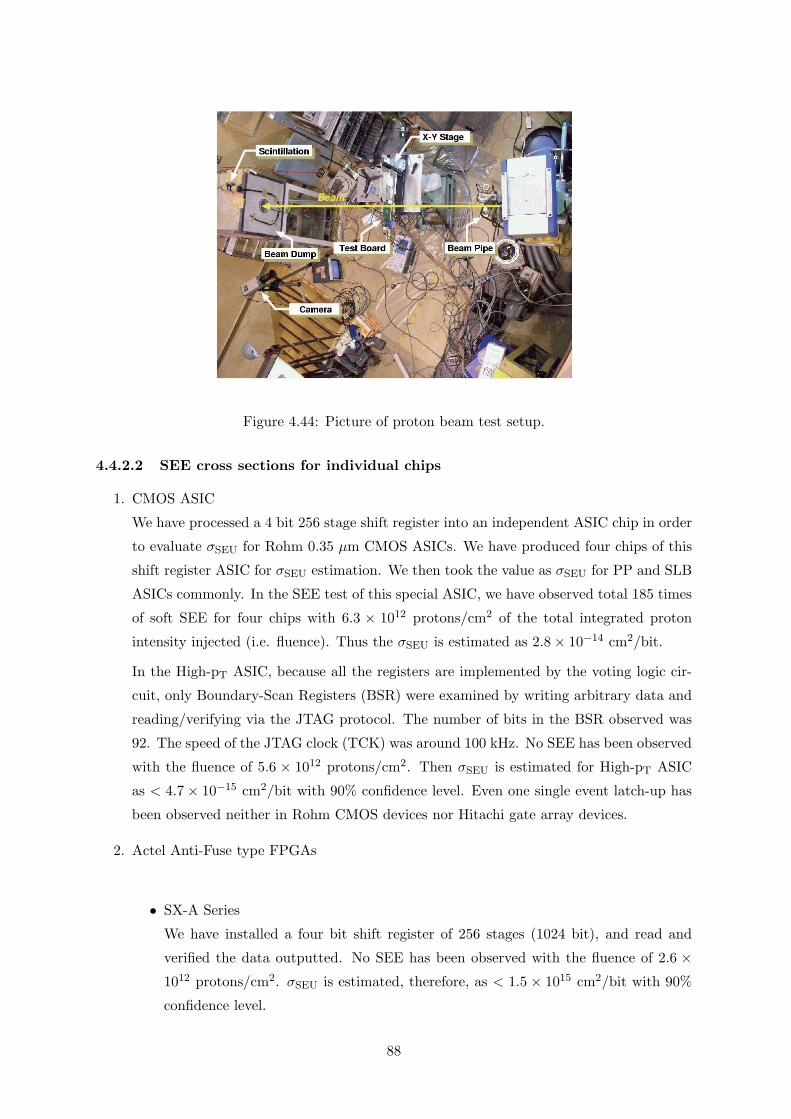
Figure 4.44: Picture of proton beam test setup.
4.4.2.2 SEE cross sections for individual chips
1. CMOS ASIC
We have processed a 4 bit 256 stage shift register into an independent ASIC chip in order
to evaluate σSEU for Rohm 0.35 µm CMOS ASICs. We have produced four chips of this
shift register ASIC for σSEU estimation. We then took the value as σSEU for PP and SLB
ASICs commonly. In the SEE test of this special ASIC, we have observed total 185 times
of soft SEE for four chips with 6.3 × 10¹² protons/cm2 of the total integrated proton
intensity injected (i.e. fluence). Thus the σSEU is estimated as 2.8 × 10⁻¹⁴ cm2/bit.
In the High-pT ASIC, because all the registers are implemented by the voting logic cir-
cuit, only Boundary-Scan Registers (BSR) were examined by writing arbitrary data and
reading/verifying via the JTAG protocol. The number of bits in the BSR observed was
92. The speed of the JTAG clock (TCK) was around 100 kHz. No SEE has been observed
with the fluence of 5.6 × 10¹² protons/cm2. Then σSEU is estimated for High-pT ASIC
as < 4.7 × 10⁻¹⁵ cm2/bit with 90% confidence level. Even one single event latch-up has
been observed neither in Rohm CMOS devices nor Hitachi gate array devices.
2. Actel Anti-Fuse type FPGAs
• SX-A Series
We have installed a four bit shift register of 256 stages (1024 bit), and read and
verified the data outputted. No SEE has been observed with the fluence of 2.6 ×10¹² protons/cm2. σSEU is estimated, therefore, as < 1.5 × 1015 cm2/bit with 90%
confidence level.
88
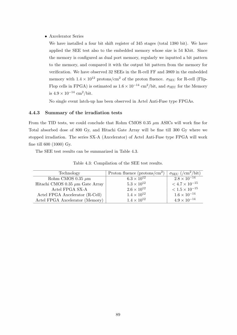
• Axcelerator Series
We have installed a four bit shift register of 345 stages (total 1380 bit). We have
applied the SEE test also to the embedded memory whose size is 54 Kbit. Since
the memory is configured as dual port memory, regularly we inputted a bit pattern
to the memory, and compared it with the output bit pattern from the memory for
verification. We have observed 32 SEEs in the R-cell FF and 3869 in the embedded
memory with 1.4 × 10¹² protons/cm2 of the proton fluence. σSEU for R-cell (Flip-
Flop cells in FPGA) is estimated as 1.6× 10⁻¹⁴ cm2/bit, and σSEU for the Memory
is 4.9 × 10⁻¹⁴ cm2/bit.
No single event latch-up has been observed in Actel Anti-Fuse type FPGAs.
4.4.3 Summary of the irradiation tests
From the TID tests, we could conclude that Rohm CMOS 0.35 µm ASICs will work fine for
Total absorbed dose of 800 Gy, and Hitachi Gate Array will be fine till 300 Gy where we
stopped irradiation. The series SX-A (Axcelerator) of Actel Anti-Fuse type FPGA will work
fine till 600 (1000) Gy.
The SEE test results can be summarized in Table 4.3.
Table 4.3: Compilation of the SEE test results.
Technology Proton fluence (protons/cm2) σSEU (/cm2/bit)Rohm CMOS 0.35 µm 6.3 × 10¹² 2.8 × 10⁻¹⁴
Hitachi CMOS 0.35 µm Gate Array 5.3 × 10¹² < 4.7 × 10⁻¹⁵
Actel FPGA SX-A 2.6 × 10¹² < 1.5 × 10⁻¹⁵
Actel FPGA Axcelerator (R-Cell) 1.4 × 10¹² 1.6 × 10⁻¹⁴
Actel FPGA Axcelerator (Memory) 1.4 × 10¹² 4.9 × 10⁻¹⁴
89
Chapter 5
Summary and Conclusions
In the ATLAS Experiment, events with important and/or interesting physics processes are
buried in a large amount of backgrounds originated from QCD soft collision processes. Event
triggering system plays an important role to find out such interesting events, and will be a key
for success in the experiment. Since muons exist in the final states of various important physics
processes, trigger systems with muon activities is especially important in this experiment.1
The author developed two the key devices for the Endcap muon Trigger of the Level-1
Trigger system; TGC Trigger system.
The TGC Trigger electronics is required to handle about 3×10⁵ chamber signals, to operate
in synchronous with 40.08 MHz LHC clock and to have dead-time less architecture (pipe-line
processing). To realize the functionalities, various new technologies were tested and introduced
to the trigger system. Followings were accomplished in this studies :
1. Development of the front-end circuits with ASICs (Slave Board ASICs) :
In SLB ASIC, five types of low-pT decision circuits are implemented in one device. It also
has pipeline memories to realize dead-time-less data acquisition (pipeline processing) and
queuing buffers for signal readout. We implemented the circuits in a custom IC device
(Rohm 0.35 µm process with 9.86 mm squared die), where a total number of ∼ 106 CMOS
gates were placed. The author also confirmed the validity of the fabricated ASICs. The
ASICs worked with a clock frequency up to 69 MHz (i.e. There is 10.5 ns timing margin
at normal 40.08 MHz operation.). The mass-production had done.
2. Development of the (R, φ) coordinate integration logic (Sector Logic) :
The Sector Logic integrates R and φ coordinate information and finds muons with high
transverse momentum. To remain a flexibility for detection of various types of the physics
events, the Look-Up Table (LUT) algorithm is implemented in FPGA (programmable)
devices. In the Sector Logic, muons are classified into six groups based on the momentum
1Note that muons, which punch-through the calorimeters, make signals in the outer tracker devices. Hits inthe tracker are important as clean trigger sources rather than the hits observed in the inner tracking systemswhere a large amount of pile-up is seen.
90

with the programmable thresholds. The author started from a preliminary designing
process of the algorithm, and by completing the design verification, module prototyping
for the validity check, then, in final, established the final design for the fabrication. With
the prototyping module, the author confirmed that the module worked with a clock
frequency up to 54 MHz. It was found that the signal processing worked enough fast and
provided 6.5 ns margin at normal 40.08 MHz operation.
3. Tests for radiation tolerance :
Electronics systems, which will be installed in the experimental hall, are required to
be radiation-tolerant. According the latest ATLAS policy [14], the electronics devices
mounted around the TGC should be tolerant to 210 Gy for TID and 2.1×10¹⁰ hadrons/cm2
for SEE.
• Tests for total ionization doze (TID) effects; caused by γ-rays :
We measured variations of the characteristics of the ASICs (Rohm 0.35 µm CMOS
process, Hitachi 0.35 µm Gate Array CMOS process) and two Actel Anti-Fuse type
FPGAs as a function of total radiation dose. The leakage current does not increase
until the radiation exposure of 210 Gy, which is the Radiation Tolerance Criteria
(RTC) value. Note that this RTC value contains safety factor 70 to the simulated
radiation level in worst case for 10 years operation. And any fatal phenomena were
occurred. Hence, it can be concluded that this device can be used for ATLAS
Experiment without any TID problem.
• Tests for single event effects (SEE); caused by energetic hadron (>20MeV):
We have measured the rates of single event upset (SEU) for the ICs with protons
(70 MeV) provided from the AVF-Cyclotron at CYRIC in Tohoku University. The
SEU cross-section of Rohm 0.35 µm CMOS process measured from this experiment
is σSEU = 2.8 × 10⁻¹⁴ cm2/bit. Since the estimated SEU rate in the whole TGC
electronics system is small enough, we can overcome it by introducing the Voting
Logic structure.
91

Bibliography
[1] ATLAS Collaboration, “Technical Proposal for a General-Purpose pp Experiment at the
Large Hadron Collider at CERN”, CERN/LHCC/94-43, December 15, 1994.
[2] O.Bruning et. al., “LHC Design Report Volume I The LHC Main Ring”, CERN-2004-003,
June 4, 2004.
[3] The ATLAS and CMS Collaborations, “High Transverse Momentum Physics at the Large
Hadron Collider”, BNL-HET-01/33.
[4] RD12 Collaboration, “RD12 Status Report”, CERN/LHCC/97-29, April 1997.
[5] ATLAS Collaboration, “ATLAS Detector and Performance Technical Design Report”,
CERN/LHCC/99-14,15 (1999)
[6] ATLAS Collaboration, “ATLAS Level-1 Trigger Technical Design Report”,
CERN/LHCC/98-14, June 1998.
[7] ATLAS Collaboration, “ATLAS Muon Spectrometer Technical Design Report”,
CERN/LHCC/97-22, May 1997.
[8] ATLAS Collaboration, “ATLAS Liquid Argon Calorimeter Technical Design Report”,
CERN/LHCC/96-41, December 1996.
[9] ATLAS Collaboration, “ATLAS Tile Calorimeter Technical Design Report”,
CERN/LHCC/96-42, December 1996.
[10] ATLAS Collaboration, “ATLAS Trigger Performance Status Report”, CERN/LHCC/98-
15, June 1998.
[11] P.Igo-Kemenes, “report to the LEPC”, November 2000.
[12] O.Sasaki, “Official Radiation Levels and Radiation Tolerance Criteria in TGC Boards”,
http://www-online.kek.jp/˜sosamu/radiation/radiationtolerancecriteria tgc.doc
[13] Level-1 muon trigger group, “Improvement to the Level-1 muon trigger giving in-
creased robustness against backgrounds”, ATLAS-DAQ-99-008 (ATLAS-COM-DAQ-99-
92

011), June 1, 1999.
http://atlas.web.cern.ch/Atlas/project/TGC/www/doc/com-daq-99-011 ps.gz
[14] Radiation Hardness Assurance Working Group, “ATLAS policy on radiation tolerant elec-
tronics”, ATLAS working document.
http://www.cern.ch/Atlas/GROUPS/FRONTEND/WWW/radtol2.ps
[15] ATLAS Radiation Background Taskforce, “Estimation of Radiation Background, Impact
on Detectors, Activation and Shielding Optimization in ATLAS”, ATL-GEN-2005-001,
January 13, 2005.
http://atlas.web.cern.ch/Atlas/GROUPS/PHYSICS/RADIATION/gen-2005-001-feb05.pdf
[16] Ph.Farthouat, “Interfaces and overlaps in the level-1 muon trigger system, Revision 11”,
January 17, 2006. https://edms.cern.ch/document/114604/5
[17] R.Ichimiya, “HPT Board g-link connection table (rev-12)”, ATL-DA-EN-0002,
July 29, 2005, https://edms.cern.ch/document/700560/
[18] R.Ichimiya et. al., “Sector Logic Implementation for the ATLAS Endcap Level-1 Muon
Trigger”, Proceedings of the Eights Workshop on Electronics for LHC Experiments, Col-
mar, France, 9-13 September 2002, CERN 2002-003, pp. 236-240.
[19] R.Ichimiya et. al., “Report on the Integration Test between the Endcap Muon Trigger
Sector Logic and the Muon-CTP-Interface”, ATL-DA-TR-0004, January 10, 2002.
[20] R.Ichimiya et.al., “Radiation Qualification of Electronics Components used for the ATLAS
Level-1 Muon Endcap Trigger System”, IEEE Transaction on Nuclear Science, Vol.52,
issue 4, August 2005, pp.1061-1066.
http://cdsweb.cern.ch/search.py?recid=812814&ln=en
[21] R.Ichimiya et. al., “Irradiation tests of ROHM 0.35um ASIC and Actel Anti-fuse FPGA
for the ATLAS Muon Endcap Level-1 Trigger System”, Proceedings of the Tenth Workshop
on Electronics for LHC Experiments, Boston, MA, USA, 13-17 September, 2004, CERN
2004-010, pp. 117-121.
http://cdsweb.cern.ch/search.py?recid=812812&ln=en
[22] R.Ichimiya et. al., “Radiation qualification of Commercial-Off-The-Shelf LVDS and G-
link serializers and deserializers for the ATLAS endcap muon level-1 trigger System”,
Proceedings of the Tenth Workshop on Electronics for LHC Experiments, Boston, MA,
USA, 13-17 September 2004, CERN 2004-010, pp. 389-393.
http://cdsweb.cern.ch/search.py?recid=812813&ln=en
93
[23] O.Sasaki, “ATLAS Thin Gap Chamber Amplifier-Shaper-Discriminator ICs and ASD
Boards”, ASD PRR document, ATL-MT-ER-0001, October, 1999.
https://edms.cern.ch/file/325796/1/asd-prr.pdf
[24] O.Sasaki and M.Yoshida, “ASD IC for the thin gap chamber in the ATLAS experiment”,
IEEE Transaction on Nuclear Science, Vol.46 (1999) pp. 1871-1875.
[25] The TGC Excel Parameter Book.
http://atlas.web.cern.ch/Atlas/project/TGC/design/tgc.xls
[26] H.Kano et. al., “Custom chips developed for the trigger/readout system of the ATLAS
endcap muon chambers”, Proceedings of the Sixth Workshop on Electronics for LHC Ex-
periments, Cracow, Poland, 11-15 September 2002, CERN 2000-010, pp. 486-490.
[27] H.Sakamoto et. al., “Readout system for the ATLAS end cap muon trigger chamber”,
Prepared for 7th International Conference on Instrumentation for Colliding Beam Physics
(INSTR99), Hamamatsu, Japan, 15-19 November, 1999. Published in Nuclear Instruments
and Methods in Physics Research Section A, Vol.453, Issues 1-2, 11 October 2000, pp. 430-
432.
[28] K.Hasuko et. al., “A remote control system for FPGA-embedded modules in radiation
Environments”, IEEE transactions on Nuclear Science, vol49 (2002), issue 2, pp. 501-506.
[29] K.Hasuko et. al., “The first integration test of the ATLAS end-cap muon level1 Trigger
system”, Prepared for IEEE 2002 Nuclear Science Symposium (NSS) and Medical Imaging
Conference (MIC) and Symposium on Nuclear Power Systems, Norfolk, Virginia, 10-16
November 2002. Published in IEEE Transaction on Nuclear Science, Vol.50 (2003) pp. 864-
868.
[30] T.Maeno et. al., “Test Beam results on the ATLAS First Level-1 Endcap Muon Trigger
System”, Published in Como 2003, Astroparticle, particle and space physics, detectors and
Medical physics applications, pp. 265-269.
[31] C.Fukunaga et. al., “Beam test of the ATLAS End-cap Muon Level1 Trigger System”, Pro-
ceedings of the Ninth Workshop on Electronics for LHC Experiments, Amsterdam Nether-
land, Sep. 2003.
[32] The LVDS (Low Voltage Differential Signaling) Standard, ANSI/TIA/EIA-644.
[33] National Semiconductor, “LVDS Owner’s Manual and Design Guide”.
http://www.national.com/appinfo/lvds/lvdstotal.pdf
[34] IEEE, “IEEE Standard Test Access Port and Boundary-Scan Architecture”,
IEEE Std. 1149.1-1990.
94
[35] IEEE, “Supplement to IEEE Std. 1149.1-1990, IEEE Standard Test Access Port and
Boundary-Scan Architecture”, IEEE Std. 1149.1b-1994.
[36] JTAG Technologies web page, http://www.jtag.com
[37] Xilinx Inc., 2100 Logic Drive San Jose, CA 95124 USA.
http://www.xilinx.com/
[38] Actel Corporation, Mountain View, CA 94043-4655 USA.
http://www.actel.com/
[39] A.H.Johnston, “Radiation Damage of Electronic and Optoelectronic Devices in Space”,
Proceedings of the 4th International Workshop on Radiation Effects on Semiconductor
Devices for Space Application.
http://parts.jpl.nasa.gov/docs/Dmg Space-00.pdf
[40] T.Miyahira and G.Swift, “Evaluation of Radiation Effects in Flash Memories”, Proceedings
of 1998 Military and Aerospace Applications of Programmable Devices and Technologies
Conference.
http://klabs.org/richcontent/MAPLDCon98/Abstracts/c4.htm
[41] D.R.Roth et. al., “SEU and TID testing of the Samsung 128 Mbit and the Toshiba 256
Mbit Flash memory”, 2000 IEEE Radiation Effect Data Workshop, pp. 96-99.
[42] Fuji Photo Film Co., Ltd.
See http://home.fujifilm.com/products/science/img plate/img plate.html
95