ac/dc controller ic for led lighting included 650v mosfet€¦ · ac revision function for led...
TRANSCRIPT
Datasheet
Product structure:Silicon monolithic integrated circuit This product has no designed protection against radioactive rays. .
1/13
Target SPEC Ver.00127.JUN.2013
© 2013 ROHM Co., Ltd. All rights reserved. TSZ22111・14・001
www.rohm.com
AC/DC Drivers
AC/DC controller IC for LED lighting Included 650V MOSFET BM520Q2XF Series ((((In Developing)))) Description
BM520Q2xF is AC/DC converter with a built in FET which has a 650V withstand voltage for LED lighting. This IC is suitable for a Quasi-resonant switching typed High Side LED driver application, it can achieve a high accuracy of the LED current, and a low EMI at once. In addition, by embedding a PFC (Power Factor Correction) converter, it provides a countermeasure for harmonics.
Moreover, owing to the built-in bootstrap circuit with 650V withstand voltage, the low-power can be achieved. And owing to the external resistance for sensing the switching current, you may design the power supply with a high degree of freedom.
By the built-in bootstrap circuit and MOSFET, a compact application board with only a few components can be designed easily. So this IC is also suitable for a low cost strategy.
Key Specifications
Operating Power Supply Voltage Range:
VCC 8.9V to 26.0V DRAIN:~650V Operating Current: Normal: ( BM520Q25F ):0.60mA (Typ.) ( BM520Q29F ):0.50mA (Typ.) Operating temperature range: - 40deg. to +105deg. MOSFET ON resistance: BM520Q25F :4.0Ω (Typ.) BM520Q29F :8.5Ω (Typ.)
Features Quasi-resonant switching mode + PFC Built-in 650V bootstrap circuit Built-in 650V switching MOSFET Maximum frequency 150kHz VCC pin: under voltage protection VCC pin: over voltage protection (latch) SOURCE pin: Leading-Edge-Blanking function LED over current detection ZT pin: trigger mask function ZT pin: over voltage protection (latch) FET over current protection AC revision function for LED current detection
Package
SOP8 4.90mm×3.90mm pitch 1.27mm (Typ.) (Typ.) (Typ.)
Application
LED bulb, seal typed LED lighting Electrical machineries for LED lighting
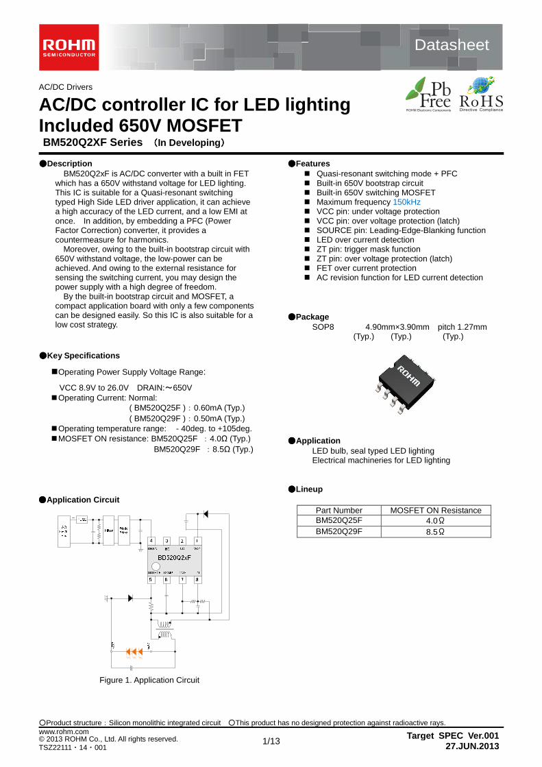
LineupApplication Circuit
Part Number MOSFET ON Resistance BM520Q25F 4.0Ω BM520Q29F 8.5Ω
Figure 1. Application Circuit
2/13
DatasheetBM520Q2XF Series
Target SPEC Ver.00127.JUN.2013
© 2013 ROHM Co., Ltd. All rights reserved. www.rohm.com
TSZ22111・15・001
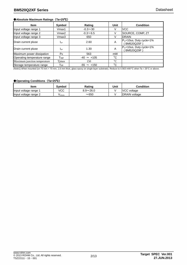
Absolute Maximum Ratings((((Ta=25))))
Item Symbol Rating Unit Condition Input voltage range 1 Vmax1 -0.3~30 V VCC Input voltage range 2 Vmax2 -0.3~6.5 V SOURCE, COMP, ZT Input voltage range 3 Vmax3 650 V DRAIN
Drain current pluse IDP 2.60 A PW=10us, Duty cycle=1% ( BM520Q25F )
Drain current pluse IDP 1.30 A PW=10us, Duty cycle=1% ( BM520Q29F )
Maximum power dissipation Pd 563 mW Operating temperature range Topr -40 ~ +105 oC Maximum junction temperature Tjmax 150 oC Storage temperature range Tstr -55 ~ +150 oC (Note1) When mounted (on 70 mm × 70 mm, 1.6 mm thick, glass epoxy on single-layer substrate). Reduce to 4.563 mW/°C when Ta = 25°C or above. Operating Conditions((((Ta=25))))
Item Symbol Rating Unit Condition Input voltage range 1 VCC 8.9~26.0 V VCC voltage Input voltage range 2 VDRAIN ~650 V DRAIN voltage
3/13
DatasheetBM520Q2XF Series
Target SPEC Ver.00127.JUN.2013
© 2013 ROHM Co., Ltd. All rights reserved. www.rohm.com
TSZ22111・15・001
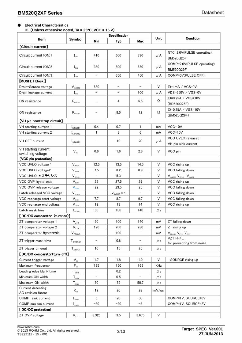
Electrical Characteristics IC((((Unless otherwise noted, Ta = 25°°°°C, VCC = 15 V))))
Item Symbol SpecificationSpecificationSpecificationSpecification
UnitUnitUnitUnit ConditionConditionConditionCondition
MinMinMinMin TypTypTypTyp MaxMaxMaxMax
[[[[Circuit current]]]]
Circuit current (ON)1 ION1
410 600 790 μA
NTC=2.0V(PULSE operating)
BM520Q25F
Circuit current (ON)2 ION2
350 500 650 μA
COMP=2.0V(PULSE operating)
BM520Q29F
Circuit current (ON)3 ION3
- 350 450 μA COMP=0V(PULSE OFF)
[MOSFET b[MOSFET b[MOSFET b[MOSFET block ]lock ]lock ]lock ]
Drain-Source voltage V(BR)DDS
650 - - V ID=1mA / VGS=0V
Drain leakage current IDSS
- - 100 μA VDS=650V / VGS=0V
ON resistance RDS(ON)
- 4 5.5 Ω
ID=0.25A / VGS=10V
(BD520Q25F)
ON resistance RDS(ON)
- 8.5 12 Ω
ID=0.25A / VGS=10V
(BM520Q29F)
[[[[VHVHVHVH pinpinpinpin bootstrap circuit]]]]
VH starting current 1 ISTART1
0.4 0.7 1 mA VCC= 0V
VH starting current 2 ISTART2
1 3 6 mA VCC=10V
VH OFF current ISTART3
- 10 20 μA
VCC UVLO released
VH pin sink current
VH starting current switching voltage
VSC
0.6 1.6 2.8 V VCC pin
[[[[VCCVCCVCCVCC pin protectionpin protectionpin protectionpin protection]]]]
VCC UVLO voltage 1 VUVLO1
12.5 13.5 14.5 V VCC rising up
VCC UVLO voltage2 VUVLO2
7.5 8.2 8.9 V VCC falling down
VCC UVLO ヒステリシス VUVLO3
- 5.3 - V VUVLO3=
VUVLO1-
VUVLO2
VCC OVP hysteresis VOVP1
26 27.5 29 V VCC rising up
VCC OVP release voltage VOVP2
22 23.5 25 V VCC falling down
Latch released VCC voltage VLATCH
- VUVLO2
-0.5 - V VCC falling down
VCC recharge start voltage VCHG1
7.7 8.7 9.7 V VCC falling down
VCC recharge end voltage VCHG2
12 13 14 V VCC rising up
Latch mask time TLATCH
60 100 140 μs
[ DC/DC[ DC/DC[ DC/DC[ DC/DC comparator comparator comparator comparator ((((turnturnturnturn----onononon))))]]]]
ZT comparator voltage 1 VZT1
60 100 140 mV ZT falling down
ZT comparator voltage 2 VZT2
120 200 280 mV ZT rising up
ZT comparator hysteresis VZTHYS
- 100 - mV VZTHYS=
VZT1-
VZT2
ZT trigger mask time TZTMASK
- 0.6 - μs
VZT H->L,
for preventing from noise
ZT trigger timeout TZTOUT
10 15 25 μs
[ DC/DC[ DC/DC[ DC/DC[ DC/DC comparatorcomparatorcomparatorcomparator((((turnturnturnturn----offoffoffoff))))]]]]
Current trigger voltage VCS
1.7 1.8 1.9 V SOURCE rising up
Maximum frequency FSW
135 150 165 KHz
Leading edge blank time TLEB
- 0.2 - μs
Minimum ON width Tmin
- 0.5 - μs
Maximum ON width Tmax
30 39 50.7 μs
Current detecting
AC revision factor
KCS
12 20 28 mV/us
COMP sink current ICompsi
5 20 50 COMP=1V, SOURCE=0V
COMP sou rce surrent Icompso
-50 -20 -5 COMP=1V, SOURCE=2V
[ DC/DC [ DC/DC [ DC/DC [ DC/DC protectioprotectioprotectioprotectionnnn]]]]
ZT OVP voltage VZTL
3.325 3.5 3.675 V
4/13
DatasheetBM520Q2XF Series
Target SPEC Ver.00127.JUN.2013
© 2013 ROHM Co., Ltd. All rights reserved. www.rohm.com
TSZ22111・15・001
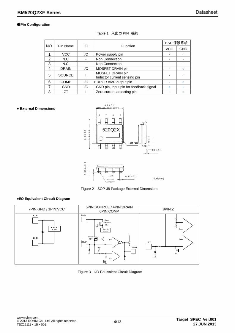
Pin Configuration
Table 1. 入出力 PIN 機能
NO. Pin Name I/O Function ESD 保護系統
VCC GND
1 VCC I/O Power supply pin - 2 N.C. - Non Connection - - 3 N.C. - Non Connection - - 4 DRAIN I/O MOSFET DRAIN pin -
5 SOURCE I MOSFET DRAIN pin Inductor current sensing pin -
6 COMP I/O ERROR AMP output pin - 7 GND I/O GND pin, input pin for feedback signal - 8 ZT I Zero current detecting pin -
External Dimensions
I/O Equivalent Circuit Diagram
7PIN:GND / 1PIN:VCC 5PIN:SOURCE / 4PIN:DRAIN
6PIN:COMP 8PIN:ZT
Super
Junction
FET
Drain
Source
Start Up
Circuit
Power
FET
COMP
ZT
0.4
5M
IN
0 . 2± 0 . 1
1 . 2 7
1.3
75±
0.1
0.1
75
0 . 4 2± 0 . 1
4 . 9± 0 . 2
1
2
3 4
8
7
6
5
6.0
±0
.3
3.9
±0
.2
MAX 5.25 ( include BURR)
(Unit:mm) 1.27
520Q2X
Lot No.
Figure 2 SOP-J8 Package External Dimensions
Figure 3 I/O Equivalent Circuit Diagram
5/13
DatasheetBM520Q2XF Series
Target SPEC Ver.00127.JUN.2013
© 2013 ROHM Co., Ltd. All rights reserved. www.rohm.com
TSZ22111・15・001
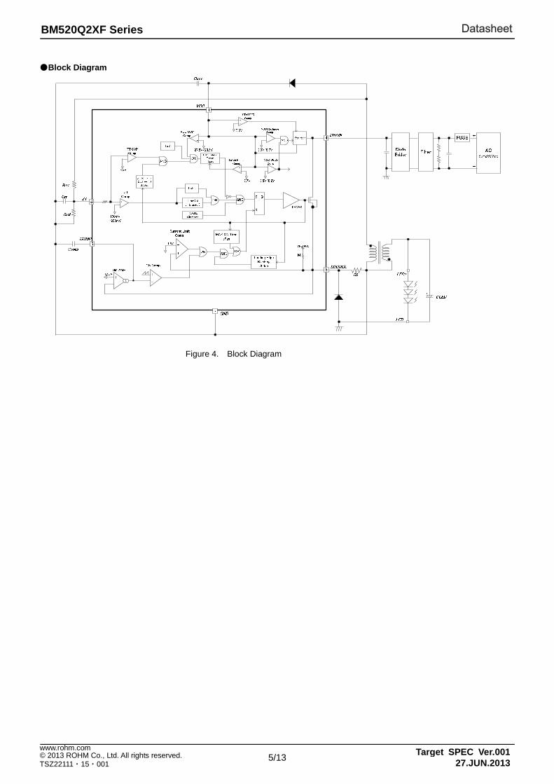
Block Diagram
Figure 4. Block Diagram
6/13
DatasheetBM520Q2XF Series
Target SPEC Ver.00127.JUN.2013
© 2013 ROHM Co., Ltd. All rights reserved. www.rohm.com
TSZ22111・15・001
Start U
p C
urrent [m
A]
+
-VCC RECHARGE
VCC
Cvcc
DRAINFUSE
+
-
Diode
Bridge
AC
Input
4
1
13V/8.7V
+
-
VSC
LH
LH
Starter
0.8V
+
-
13.5V/8.2V
VCC UVLO
Block Descriptions
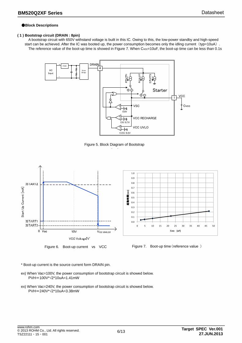
( 1 ) Bootstrap circuit (DRAIN : 8pin) A bootstrap circuit with 650V withstand voltage is built in this IC. Owing to this, the low-power standby and high-speed start can be achieved. After the IC was booted up, the power consumption becomes only the idling current(typ=10uA).
The reference value of the boot-up time is showed in Figure 7. When Cvcc=10uF, the boot-up time can be less than 0.1s
* Boot-up current is the source current form DRAIN pin.
ex) When Vac=100V, the power consumption of bootstrap circuit is showed below. PVH=100V*√2*10uA=1.41mW ex) When Vac=240V, the power consumption of bootstrap circuit is showed below. PVH=240V*√2*10uA=3.38mW
0.0
0.1
0.2
0.3
0.4
0.5
0.6
0.7
0.8
0.9
1.0
0 5 10 15 20 25 30 35 40 45 50
起動
時間
起動
時間
起動
時間
起動
時間
[se
c]
Cvcc [uF]
Figure 5. Block Diagram of Bootstrap circuit
Figure 6. Boot-up current vs VCC
voltage
Figure 7. Boot-up time(reference value )
7/13
DatasheetBM520Q2XF Series
Target SPEC Ver.00127.JUN.2013
© 2013 ROHM Co., Ltd. All rights reserved. www.rohm.com
TSZ22111・15・001
(2 )起動起動起動起動シーケンスシーケンスシーケンスシーケンス 起動シーケンスを Figure 8 に示します。 各々の詳細な説明は、各章で説明します。
Figure 8. 起動シーケンス タイムチャート
A : Input voltage VH is applied.
B : The IC starts operating when VCC > VUVLO1 (13.5 V Typ). Switching function starts when other protection functions are judged as normal. During the time from the IC starts up until the secondary output voltage increases higher than certain voltage, the current consumption of VCC pin causes a drop of VCC voltage. As a result, the VCC should be set to higher than VUVLO2
(8.2V Typ) until the switching operation starts. C : Owing to the soft-start function, over current limit value is restricted to prevent any excessive rise in voltage or current.
D : When the switching operation starts, VOUT rises. Once the output voltage starts, set the rated voltage within the TFOLP period (32ms Typ). E : When there is a light load, it makes FB voltage < VBST (0.40V Typ). In this case, burst operation starts for reducing power consumption. While the burst operation works, the IC is in a low-power consumption mode. H : If the VCC voltage becomes lower than VUVLO2
(7.7V Typ), the restart is executed. I : The circuit current of IC reduces, and the voltage of VCC pin rises. (same as B) J : Same as F. K : Same as G.
TBD

8/13
DatasheetBM520Q2XF Series
Target SPEC Ver.00127.JUN.2013
© 2013 ROHM Co., Ltd. All rights reserved. www.rohm.com
TSZ22111・15・001
(3) VCC pin protection function The VCC low voltage protection function VCC UVLO (Under Voltage Lock Out), over voltage protection function VCC OVP (Over Voltage Protection), and a VCC recharge function which operates in case of a drop in VCC voltage are built in this IC. The VCC UVLO and VCC OVP functions are used for preventing the destructions of the switching MOSFET which occurs when the VCC voltage is too high or too low. Owing to the VCC charge function, the VCC pin is charged from high voltage lines by the start circuit when the VCC voltage drops, and the secondary output voltage is stabilized.
(3-1) VCC UVLO / VCC OVP function
VCC UVLO and VCC OVP are auto recovery comparators which have voltage hysteresis. VCC OVP operates in case of continuing VCC pin voltage > VOVP
(Typ=27.5V). VCC OVP has a built-in mask time TLATCH(Typ=100us). When the VCC voltage is over VOVP(typ=27.5V),and this state lasts TLATCH(typ=100us), the detection is executed. By this function, the surge which occurs at VCC pin can be masked .
(3-2) VCC charge function When the VCC pin voltage is over VUVLO1, the IC starts up. In this case, if the VCC pin voltage drops below VCHG1, VCC charge function operates. At this time, the VCC pin is charged from the DRAIN pin through the bootstrap circuit. By this operation, the failure of start-up can be prevented.
A: DRAIN pin voltage is applied, VCC voltage rises by the charging current Istart1 (700uA typ). B: VCC voltage> Vsc, the charging current to VCC changes from start1(700uA typ)⇒Istart2(3mA typ) C: VCC voltage> Vchg2, though VCC charge function reacts, due to VCC UVLO is detected, the charge continues. D: VCC voltage> Vuvlo1, the VCC UVLO is released, and DC/DC operation starts, the charge to VCC stops. E: VCC voltage> Vchg1, the charge to VCC restarts. F: VCC voltage> Vovp1, VCC OVP is detected. G: VCC voltage> Vovp2, if VCC voltage drops below Vovp2 in 100us, VCC OVP is released, and the latch will not be activated. H: Vovp2< VCC voltage < Vovp1, if this state is kept longer than 100us, switching stops by latch. I: VCC voltage< Vuvlo1, VCC UVLO is detected. J : VCC voltage< Vlatch2, the latch state is released. K : VCC voltage< Vcs 、the charging current to VCC changes from start2(3mA typ)⇒Istart1(700uA typ)
Figure 9. VCC_UVLO/ VCC_OVP / VCC Charge Function Timing Chart
9/13
DatasheetBM520Q2XF Series
Target SPEC Ver.00127.JUN.2013
© 2013 ROHM Co., Ltd. All rights reserved. www.rohm.com
TSZ22111・15・001
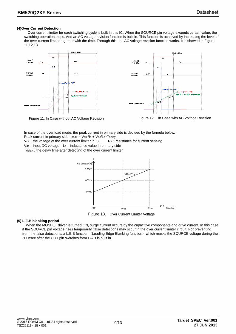
(4)Over Current Detection Over current limiter for each switching cycle is built in this IC. When the SOURCE pin voltage exceeds certain value, the
switching operation stops. And an AC voltage revision function is built in. This function is achieved by increasing the level of the over current limiter together with the time. Through this, the AC voltage revision function works. It is showed in Figure 11,12,13.
In case of the over load mode, the peak current in primary side is decided by the formula below. Peak current in primary side: Ipeak = Vcs/Rs + Vdc/Lp*Tdelay Vcs:the voltage of the over current limiter in IC Rs:resistance for current sensing Vdc:input DC voltage Lp:inductance value in primary side Tdelay:the delay time after detecting of the over current limiter
X
Y
Time [us]0.015.3us
0.400V
0.704V
7.6us
+20mV/us
0.552V
CS Limitter[V]
(5) L.E.B blanking period When the MOSFET driver is turned ON, surge current occurs by the capacitive components and drive current. In this case,
if the SOURCE pin voltage rises temporarily, false detections may occur in the over current limiter circuit. For preventing from the false detections, a L.E.B function(Leading Edge Blanking function)which masks the SOURCE voltage during the 200nsec after the OUT pin switches form L→H is built in.
Figure 11. In Case without AC Voltage Revision Figure 12. In Case with AC Voltage Revision
Figure 13. Over Current Limiter Voltage
10/13
DatasheetBM520Q2XF Series
Target SPEC Ver.00127.JUN.2013
© 2013 ROHM Co., Ltd. All rights reserved. www.rohm.com
TSZ22111・15・001
VCC
700uA Charge
(Pulse Stop)
VCC 3mA Charge
(Pulse Stop)
Normal MODE
VCC OVP
(Pulse Stop)
ZT OVP
(Pulse Stop)
TSD
(Pulse Stop)
Latch
Latch
Cancel
VCC 3mA Charge
(Latch state)
VCC 3mA Charge
(Pulse Stop)
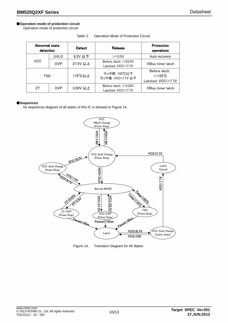
Operation mode of protection circuit Operation mode of protection circuit
Table 2. Operation Mode of Protection Circuit
Abnormal state Abnormal state Abnormal state Abnormal state
detectiondetectiondetectiondetection
DetectDetectDetectDetect ReleasReleasReleasRelease e e e
Protection Protection Protection Protection
operationsoperationsoperationsoperations
VCC
UVLO 8.2V 以下 >=13.5V Auto recovery
OVP 27.5V 以上
Before latch:<=23.5V
Latched:VCC<=7.7V
100us timer latch
TSD 175以上
ラッチ前:155以下
ラッチ後:VCC=7.7V 以下
Before latch:
<=155
Latched:VCC<=7.7V
ZT OVP 3.50V 以上
Before latch:<=3.33V
Latched:VCC<=7.7V
100us timer latch
Sequences
he sequences diagram of all states of this IC is showed in Figure 14.
Figure 14. Transition Diagram for All States

11/13
DatasheetBM520Q2XF Series
Target SPEC Ver.00127.JUN.2013
© 2013 ROHM Co., Ltd. All rights reserved. www.rohm.com
TSZ22111・15・001
Thermal loss According to the thermal design, please observe the conditions below when use this IC.
1. The ambient temperature Ta must be 105 or less. 2. The consumption of the IC must be within the allowable dissipation Pd. The thermal dissipation characteristics are as follows. (PCB: 70 mm × 70mm × 1.6 mm, mounted on glass epoxy substrate)
0
100
200
300
400
500
600
700
800
900
1000
0 25 50 75 100 125 150
Pd
[mW
]
Ta[]
Figure 15. Thermal Dissipation Characteristics

12/13
DatasheetBM520Q2XF Series
Target SPEC Ver.00127.JUN.2013
© 2013 ROHM Co., Ltd. All rights reserved. www.rohm.com
TSZ22111・15・001
Ordering Information
B M 5 2 0 Q 2 X F - GE 2
Product name
Package F : SOP8
Packaging and forming specification E2: Embossed tape and reel
Physical Dimension and Forming Specification Marking Diagram Line Up
形名形名形名形名(BM520Q2XF) BM520Q25F BM520Q29F
LOT No.
1PIN MARK
520Q2X
(UNIT : mm)
PKG : SOP8
(Max 5.35 (include.BURR))
∗ Order quantity needs to be multiple of the minimum quantity.
<Tape and Reel information>
Embossed carrier tapeTape
Quantity
Direction of feed The direction is the 1pin of product is at the upper left when you hold
reel on the left hand and you pull out the tape on the right hand
2500pcs
E2
( )
Direction of feed
Reel1pin
13/13
DatasheetBM520Q2XF Series
Target SPEC Ver.00127.JUN.2013
© 2013 ROHM Co., Ltd. All rights reserved. www.rohm.com
TSZ22111・15・001
Cautions on Use (1) Absolute maximum ratings
Operating the IC over the absolute maximum ratings may damage the IC. In addition, it is impossible to predict all destructive situations such as short-circuit modes, open circuit modes, etc. Therefore, it is important to consider circuit protection measures, like adding a fuse, in case the IC is operated in a special mode exceeding the absolute maximum ratings.
(2) Power supply lines Design the PCB layout pattern to provide low impedance ground and supply lines. Separate the ground and supply lines of the digital and analog blocks to prevent noise in the ground and supply lines of the digital block from affecting the analog block. Furthermore, connect a capacitor to ground at all power supply pins. Consider the effect of temperature and aging on the capacitance value when using electrolytic capacitors.
(3) Ground voltage The voltage of the ground pin must be the lowest voltage of all pins of the IC at all operating conditions. Ensure that no pins are at a voltage below the ground pin at any time, even during transient condition.
(4) Shorting between pins and mounting errors Be careful when mounting the IC on printed circuit boards. The IC may be damaged if it is mounted in a wrong orientation or if pins are shorted together. Short circuit may be caused by conductive particles caught between the pins.
(5) Operation under strong electromagnetic field Operating the IC in the presence of a strong electromagnetic field may cause the IC to malfunction.
(6) Input terminals In the construction of this IC, P-N junctions are inevitably formed creating parasitic diodes or transistors. The operation of these parasitic elements can result in mutual interference among circuits, operational faults, or physical damage. Therefore, conditions which cause these parasitic elements to operate, such as applying a voltage to an input pin lower than the GND voltage should be avoided. Furthermore, do not apply a voltage to the input terminals when no power supply voltage is applied to the IC. Even if the power supply voltage is applied, make sure that the input terminals have voltages within the values specified in the electrical characteristics of this IC.
(7) External capacitor When using a ceramic capacitor, determine the dielectric constant considering the change of capacitance with temperature and the decrease in nominal capacitance due to DC bias and others.
(8) Thermal consideration Use a thermal design that allows for a sufficient margin by taking into account the permissible power dissipation (Pd) in actual operating conditions.
(9) Rush current
When power is first supplied to the IC, rush current may flow instantaneously. It is possible that the charge current to the parasitic capacitance of internal photo diode or the internal logic may be unstable. Therefore, give special consideration to power coupling capacitance, power wiring, width of GND wiring, and routing of connections.
(10) Unused input terminals Input terminals of an IC are often connected to the gate of a CMOS transistor. The gate has extremely high impedance and extremely low capacitance. If left unconnected, the electric field from the outside can easily charge it. The small
charge acquired in this way is enough to produce a significant effect on the conduction through the transistor and cause unexpected operation of IC. So unless otherwise specified, input terminals not being used should be connected to the power supply or ground line.
(11) About this document Although the functional description and application notes given in this document for the IC are reliable, it does not mean that the particular application a user designs with this IC is guaranteed to work. It is the user's responsibility to check well the design application including other external devices used together with this IC.
Status of this document The Japanese version of this document is the formal specification. A customer may use this translated version only as an aid in reading the formal version. If there are any differences between the translation and formal version of this document, the formal version takes priority.