asic design implementation of memory efficient infinite
TRANSCRIPT
PRZEGLĄD ELEKTROTECHNICZNY (Electrical Review), ISSN 0033-2097, R. 88 NR 3b/2012 223
Muhammad Faisal SIDDIQI1,2 , Muhammad Kamran BHATTI4, Sana SHUJA1, Shaista JABEEN1, Saeed AHMAD1,2, Adeel IQBAL1,2 , Ghufran SHAFIQ1,2, Ahmad Naseem ALVI2, Azhar YASEEN2,
Abid Ali MINHAS5, Shahzad A. MALIK2, Shahid A. KHAN2, Raja Ali RIAZ1,2,3
Center for Advanced Studies in Telecommunication, COMSATS Institute of Information Technology, Islamabad (1), Department Of Electrical Engineering, COMSATS Institute of Information Technology, Islamabad (2), School of ECS, University of Southampton (3),
National Institute of Electronics (4), Bahria University (5)
ASIC Design Implementation of Memory Efficient Infinite Impulse Response UWB Equalizer
Abstract. Channel Equalization plays an important role in reducing distortion and Inter-Symbol Interference (ISI) to improve the quality of transmission in Ultra-Wide Band (UWB) channel. Many equalization techniques have been proposed in the past but the proposed techniques in this paper describes Infinite Impulse Response (IIR) equalizer architecture which halves the memory requirement of conventional IIR equalizers. This is achieved by exploiting the aperiodically repeated clusters of negative-exponentially decaying segments of Channel Impulse Response (CIR) and hence by providing a single delay- line between the input and output of the equalizer. Further this architecture is realized by implementing on Application Specific Integrated Circuit (ASIC) using Mentor Graphics IC Design tools. Mathematical modeling gives suitable parameters of the IIR Filter, followed by Register Transfer Level (RTL) Design using Very High Descriptive Language (VHDL), ASIC synthesis to TSMC 0.35um process technology, physical modeling using advanced layout techniques. The IIR equalization filter is designed using 8758 Metal Oxide Semi-conductor (MOS) transistors with core cell area of 0.406mm2. Streszczenie. W artykule zaproponowano architekturę ekwalizera NOI, która zmniejsza wymagania pamięci przy transmisji szerokopasmowej w układach ASIC. Zaprezentowano układ w technologii 35 nm z tranzystorami MOS przy powierzchni celki jądra 0.406 mm2. (Projekt szerokopasmowego ekwalizera NOI w układach ASIC) Keywords: Quasi-cyclic LDPC codes, Protograph LDPC codes, Low complexity LDPC codes, Vandermonde Matrix. Słowa kluczowe: układy ASIC – application specific integrated circuits, ekwalizer, filtry szerokopasmowe. Introduction
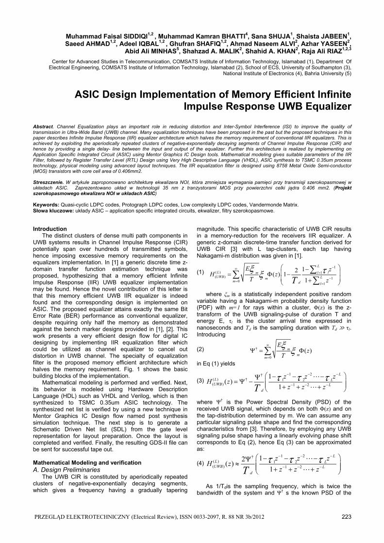
The distinct clusters of dense multi path components in UWB systems results in Channel Impulse Response (CIR) potentially span over hundreds of transmitted symbols, hence imposing excessive memory requirements on the equalizers implementation. In [1] a generic discrete time z-domain transfer function estimation technique was proposed, hypothesizing that a memory efficient Infinite Impulse Response (IIR) UWB equalizer implementation may be found. Hence the novel contribution of this letter is that this memory efficient UWB IIR equalizer is indeed found and the corresponding design is implemented on ASIC. The proposed equalizer attains exactly the same Bit Error Rate (BER) performance as conventional equalizer, despite requiring only half the memory as demonstrated against the bench marker designs provided in [1], [2]. This work presents a very efficient design flow for digital IC designing by implementing IIR equalization filter which could be utilized as channel equalizer to cancel out distortion in UWB channel. The specialty of equalization filter is the proposed memory efficient architecture which halves the memory requirement. Fig. 1 shows the basic building blocks of the implementation.
Mathematical modeling is performed and verified. Next, its behavior is modeled using Hardware Description Language (HDL) such as VHDL and Verilog, which is then synthesized to TSMC 0.35um ASIC technology. The synthesized net list is verified by using a new technique in Mentor Graphics IC Design flow named post synthesis simulation technique. The next step is to generate a Schematic Driven Net list (SDL) from the gate level representation for layout preparation. Once the layout is completed and verified. Finally, the resulting GDS-II file can be sent for successful tape out. Mathematical Modeling and verification A. Design Preliminaries
The UWB CIR is constituted by aperiodically repeated clusters of negative-exponentially decaying segments, which gives a frequency having a gradually tapering
magnitude. This specific characteristic of UWB CIR results in a memory-reduction for the receivers IIR equalizer. A generic z-domain discrete-time transfer function derived for UWB CIR [3] with L tap-clusters, each tap having Nakagami-m distribution was given in [1].
(1) 1
( ) 1( ) 1
01
12( ) 1
1
L
L lm lUWB Lm
m d l
E zH z
T zT
where ξm is a statistically independent positive random variable having a Nakagami-m probability density function (PDF) with m=1 for rays within a cluster, Φ(z) is the z-transform of the UWB signaling-pulse of duration T and energy E, τl is the cluster arrival time expressed in nanoseconds and Td is the sampling duration with Td ≫ τl. Introducing
(2) †
0
( )m
mm
Ez
T
in Eq (1) yields
(3) 1 2†
( ) † 1 2( ) 1 2
1( )
1
LL L
UWB L
d
z z zH z
z z zT
where Ψ† is the Power Spectral Density (PSD) of the received UWB signal, which depends on both Φ(z) and on the tap-distribution determined by m. We can assume any particular signaling pulse shape and find the corresponding characteristics from [3]. Therefore, by employing any UWB signaling pulse shape having a linearly evolving phase shift corresponds to Eq (2), hence Eq (3) can be approximated as:
(4) 1 2†
( ) 1 2( ) 1 2
12( )
1
LL L
UWB L
d
z z zH z
z z zT
As 1/Tdis the sampling frequency, which is twice the
bandwidth of the system and Ψ† s the known PSD of the
224 PRZEGLĄD ELEKTROTECHNICZNY (Electrical Review), ISSN 0033-2097, R. 88 NR 3b/2012
signaling-pulse, we introduce the product of these two constants as:
Fig. 1. Design Methodology
(5) †2
dT
★
Finally, upon substituting Eq (5) in Eq (4), after a few algebraic simplifications we arrive at: (6)
1
( )( ) 1
†
( )( ) 1
( )1, 2,...,
L
LLUWB
zY z
H z zX z
for L
★ ★
★
which is the required transfer function of the UWB IIR equalizer. B. Conventional IIR Equalizer Design
This design hinges on the extension of Eq (6) into a difference equation. Upon solving Eq (6) for Y(z) we obtain: (7)
( )( )
1 1
(1)
( ) : ( ) 1 ( )L L
LUWBH z Y z z X z z
IIR
★★
Finally, taking the inverse z-transform of Eq (7) gives the causal recursive difference equation for the conventional IIR UWB equalizer design in the form of:
(8) 1 1
[ ] [ ] [ ] [ ]L L
v
y n x n y n v x n w
★ ★
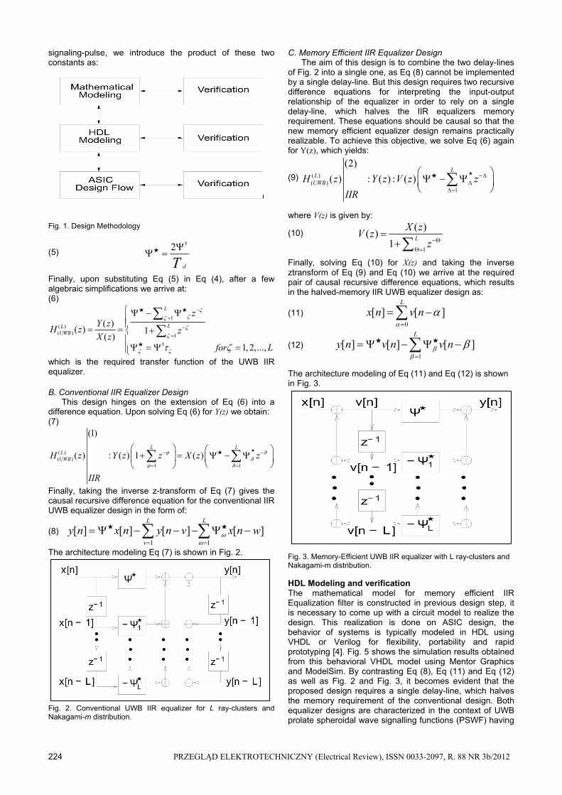
The architecture modeling Eq (7) is shown in Fig. 2. Fig. 2. Conventional UWB IIR equalizer for L ray-clusters and Nakagami-m distribution.
C. Memory Efficient IIR Equalizer Design The aim of this design is to combine the two delay-lines
of Fig. 2 into a single one, as Eq (8) cannot be implemented by a single delay-line. But this design requires two recursive difference equations for interpreting the input-output relationship of the equalizer in order to rely on a single delay-line, which halves the IIR equalizers memory requirement. These equations should be causal so that the new memory efficient equalizer design remains practically realizable. To achieve this objective, we solve Eq (6) again for Y(z), which yields:
(9) ( )( )
1
(2)
( ) : ( ) : ( )L
LUWBH z Y z V z z
IIR
★★
where V(z) is given by:
(10) 1
( )( )
1L
X zV z
z
Finally, solving Eq (10) for X(z) and taking the inverse ztransform of Eq (9) and Eq (10) we arrive at the required pair of causal recursive difference equations, which results in the halved-memory IIR UWB equalizer design as:
(11) 0
[ ] [ ]L
x n v n
(12) 1
[ ] [ ] [ ]L
y n v n v n
★ ★
The architecture modeling of Eq (11) and Eq (12) is shown in Fig. 3.
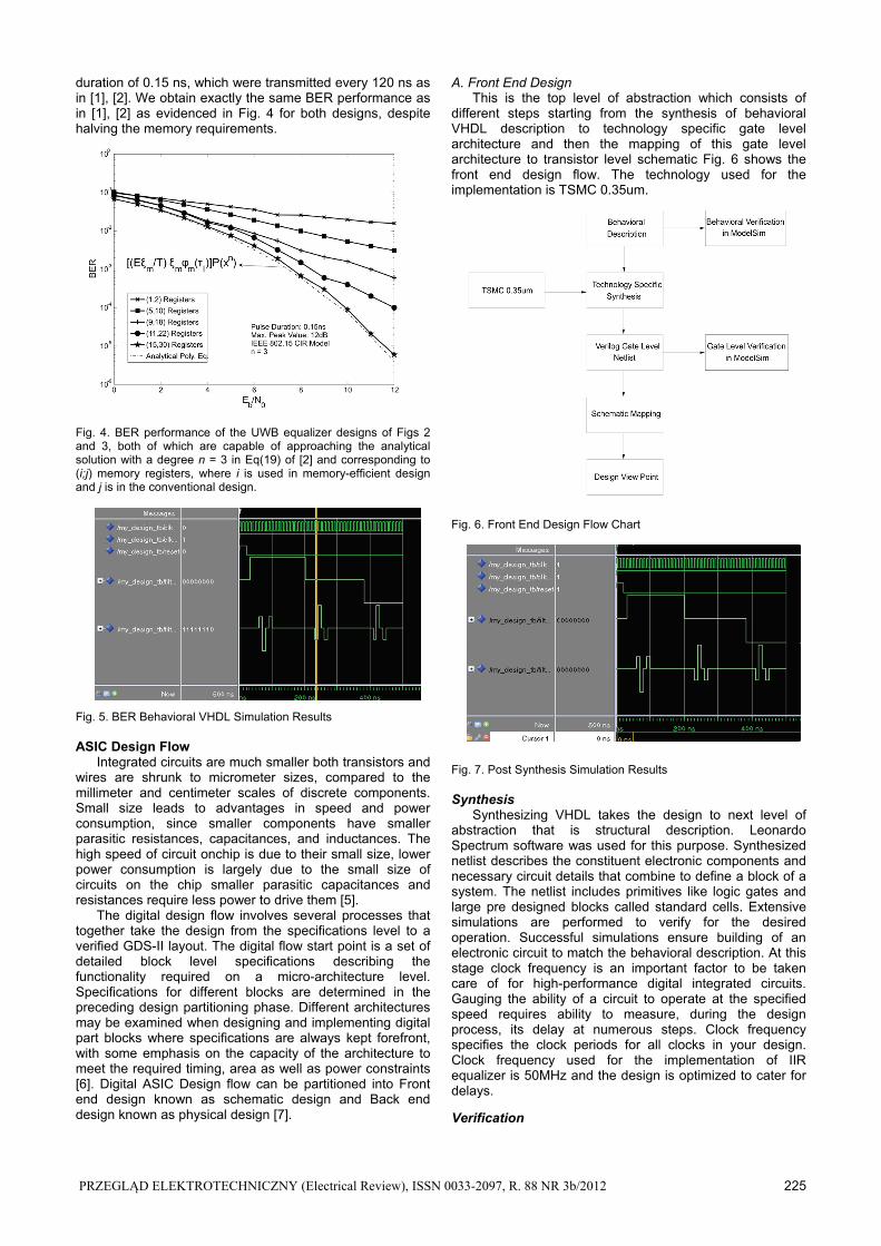
Fig. 3. Memory-Efficient UWB IIR equalizer with L ray-clusters and Nakagami-m distribution. HDL Modeling and verification The mathematical model for memory efficient IIR Equalization filter is constructed in previous design step, it is necessary to come up with a circuit model to realize the design. This realization is done on ASIC design, the behavior of systems is typically modeled in HDL using VHDL or Verilog for flexibility, portability and rapid prototyping [4]. Fig. 5 shows the simulation results obtained from this behavioral VHDL model using Mentor Graphics and ModelSim. By contrasting Eq (8), Eq (11) and Eq (12) as well as Fig. 2 and Fig. 3, it becomes evident that the proposed design requires a single delay-line, which halves the memory requirement of the conventional design. Both equalizer designs are characterized in the context of UWB prolate spheroidal wave signalling functions (PSWF) having
PRZEGLĄD ELEKTROTECHNICZNY (Electrical Review), ISSN 0033-2097, R. 88 NR 3b/2012 225
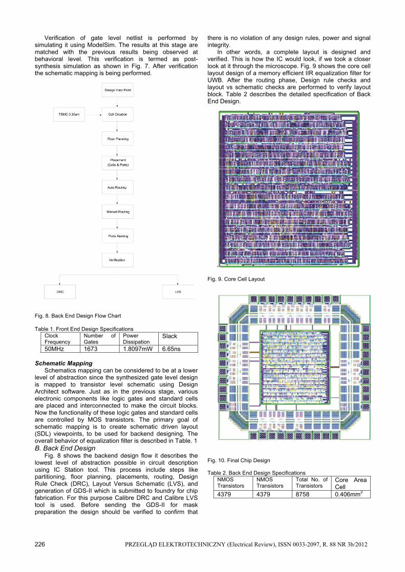
duration of 0.15 ns, which were transmitted every 120 ns as in [1], [2]. We obtain exactly the same BER performance as in [1], [2] as evidenced in Fig. 4 for both designs, despite halving the memory requirements. Fig. 4. BER performance of the UWB equalizer designs of Figs 2 and 3, both of which are capable of approaching the analytical solution with a degree n = 3 in Eq(19) of [2] and corresponding to (i;j) memory registers, where i is used in memory-efficient design and j is in the conventional design.
Fig. 5. BER Behavioral VHDL Simulation Results ASIC Design Flow
Integrated circuits are much smaller both transistors and wires are shrunk to micrometer sizes, compared to the millimeter and centimeter scales of discrete components. Small size leads to advantages in speed and power consumption, since smaller components have smaller parasitic resistances, capacitances, and inductances. The high speed of circuit onchip is due to their small size, lower power consumption is largely due to the small size of circuits on the chip smaller parasitic capacitances and resistances require less power to drive them [5].
The digital design flow involves several processes that together take the design from the specifications level to a verified GDS-II layout. The digital flow start point is a set of detailed block level specifications describing the functionality required on a micro-architecture level. Specifications for different blocks are determined in the preceding design partitioning phase. Different architectures may be examined when designing and implementing digital part blocks where specifications are always kept forefront, with some emphasis on the capacity of the architecture to meet the required timing, area as well as power constraints [6]. Digital ASIC Design flow can be partitioned into Front end design known as schematic design and Back end design known as physical design [7].
A. Front End Design This is the top level of abstraction which consists of
different steps starting from the synthesis of behavioral VHDL description to technology specific gate level architecture and then the mapping of this gate level architecture to transistor level schematic Fig. 6 shows the front end design flow. The technology used for the implementation is TSMC 0.35um. Fig. 6. Front End Design Flow Chart Fig. 7. Post Synthesis Simulation Results Synthesis
Synthesizing VHDL takes the design to next level of abstraction that is structural description. Leonardo Spectrum software was used for this purpose. Synthesized netlist describes the constituent electronic components and necessary circuit details that combine to define a block of a system. The netlist includes primitives like logic gates and large pre designed blocks called standard cells. Extensive simulations are performed to verify for the desired operation. Successful simulations ensure building of an electronic circuit to match the behavioral description. At this stage clock frequency is an important factor to be taken care of for high-performance digital integrated circuits. Gauging the ability of a circuit to operate at the specified speed requires ability to measure, during the design process, its delay at numerous steps. Clock frequency specifies the clock periods for all clocks in your design. Clock frequency used for the implementation of IIR equalizer is 50MHz and the design is optimized to cater for delays.
Verification
226 PRZEGLĄD ELEKTROTECHNICZNY (Electrical Review), ISSN 0033-2097, R. 88 NR 3b/2012
Verification of gate level netlist is performed by simulating it using ModelSim. The results at this stage are matched with the previous results being observed at behavioral level. This verification is termed as post-synthesis simulation as shown in Fig. 7. After verification the schematic mapping is being performed. Fig. 8. Back End Design Flow Chart
Table 1. Front End Design Specifications
Clock Frequency
Number of Gates
Power Dissipation
Slack
50MHz 1673 1.8097mW 6.65ns
Schematic Mapping Schematics mapping can be considered to be at a lower
level of abstraction since the synthesized gate level design is mapped to transistor level schematic using Design Architect software. Just as in the previous stage, various electronic components like logic gates and standard cells are placed and interconnected to make the circuit blocks. Now the functionality of these logic gates and standard cells are controlled by MOS transistors. The primary goal of schematic mapping is to create schematic driven layout (SDL) viewpoints, to be used for backend designing. The overall behavior of equalization filter is described in Table. 1 B. Back End Design
Fig. 8 shows the backend design flow it describes the lowest level of abstraction possible in circuit description using IC Station tool. This process include steps like partitioning, floor planning, placements, routing, Design Rule Check (DRC), Layout Versus Schematic (LVS), and generation of GDS-II which is submitted to foundry for chip fabrication. For this purpose Calibre DRC and Calibre LVS tool is used. Before sending the GDS-II for mask preparation the design should be verified to confirm that
there is no violation of any design rules, power and signal integrity.
In other words, a complete layout is designed and verified. This is how the IC would look, if we took a closer look at it through the microscope. Fig. 9 shows the core cell layout design of a memory efficient IIR equalization filter for UWB. After the routing phase, Design rule checks and layout vs schematic checks are performed to verify layout block. Table 2 describes the detailed specification of Back End Design.
Fig. 9. Core Cell Layout Fig. 10. Final Chip Design Table 2. Back End Design Specifications
NMOS Transistors
NMOS Transistors
Total No. of Transistors
Core Area Cell
4379 4379 8758 0.406mm2
PRZEGLĄD ELEKTROTECHNICZNY (Electrical Review), ISSN 0033-2097, R. 88 NR 3b/2012 227
LVS A Layout vs. Schematic (LVS) check is performed. This
ensures that the layout is in conformance with the schematic. The design process moves back and forth between Layout, LVS and DRC. DRC
This stage is often dependent on the final process technology that is used to manufacture the Chip. The design rule check ensures that the rules laid down by the fabrication process technology are not violated. A good example would be, some processes need transistors, wires and polysilicon to be of a certain minimum width. The layout would have to be drawn based on such constraints. The design toggles between Layout, LVS and DRC.
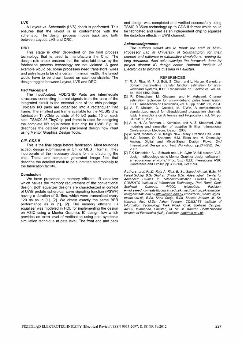
Pad Placement
The input/output, VDD/GND Pads are intermediate structures connecting internal signals from the core of the integrated circuit to the external pins of the chip package. Typically I/O pads are organized into a rectangular Pad frame. The smallest pad frame available for the MOSIS chip fabrication TinyChip consists of 40 I/O pads, 10 on each side. TSMC0.35 TinyChip pad frame is used for designing the complete IIR equalization filter chip for UWB. Fig. 10 describes the detailed pads placement design flow chart using Mentor Graphics Design Tools. CIF, GDS II
This is the final stage before fabrication. Most foundries accept design submissions in CIF or GDS II format. They incorporate all the necessary details for manufacturing the chip. These are computer generated image files that describe the detailed mask to be submitted electronically to the fabrication facility. Conclusion
We have presented a memory efficient IIR equalizer which halves the memory requirement of the conventional design. Both equalizer designs are characterized in context of UWB prolate spheroidal wave signaling function (PSWF) having a duration of 0.15ns, which were transmitted every 120 ns as in [1], [2]. We obtain exactly the same BER performance as in [1], [2]. The memory efficient IIR equalizer was modeled in HDL for implementing the design on ASIC using a Mentor Graphics IC design flow which provides an extra level of verification using post synthesis simulation technique at gate level. The front end and back
end design was completed and verified successfully using TSMC 0.35um technology up to GDS II format which could be fabricated and used as an independent chip to equalize the distortion effects in UWB channel.
Acknowledgements
The authors would like to thank the staff of Multi-Processor Lab at University of Southampton for their support and patience in exhaustive simulations, running for long durations. Also acknowlwdge the hardwork done by project director IC design centre National Institute of Electronics to promote this field in Pakistan.
REFERENCES
[1] R. A. Riaz, M. F. U. Butt, S. Chen, and L. Hanzo, Generic z-domain discrete-time transfer function estimation for ultra-wideband systems, IEEE Transactions on Electronics, vol. 44, pp. 14911492, 2008.
[2] R. Dilmaghani, M. Ghavami, and H. Aghvami, Channel estimation technique for ultra-wideband pulse transmission, IEEE Transactions on Electronics, vol. 40, pp. 13481350, 2004.
[3] A. F. Molisch, D. Cassioli, M. Z.Win, A comprehensive standardized model for ultrawideband propagation channels, IEEE Transactions on Antennas and Propogation, vol. 54, pp. 31513166, 2006.
[4] A. A. H. Ab-Rahman, I. Kamisian, and A. Z. Shaameri, Asic modeling and simulation of adaptive fir filter, International Conference on Electronic Design, 2008.
[5] W. Wolf, Modern VLSI Design. New Jersey: Prentice Hall, 2008. [6] H.G. Bakeer, O. Shaheen, H.M. Eissa and M. Dessouky,
Analog, Digital and Mixed-Signal Design Flows, 2nd International Design and Test Workshop, pp.247-252, Dec. 2007.
[7] T.K Schneider, A.J. Schwab and J.H. Aylor ”A full custom VLSI design methodology using Mentor Graphics design software in an educational environs,” Proc. Sixth IEEE International ASIC Conference and Exhibit, pp.305-308, Oct 1993.
Authors: prof. Ph.D. Raja A. Riaz, B. Sc. Saeed Ahmad, B.Sc. M. Faisal Siddiqi, B.Sc.Ghufran Shafiq, B.Sc. Adeel Iqbal , Center for Advanced Studies in Telecommunication Studies (CAST), COMSATS Institute of Information Technology, Park Road, Chak Shehzad Campus, 44000, Islamabad, Pakistan, email:[email protected],http://cast.org.pk,email:[email protected],http://ciitisb.edu.pk,email:[email protected], B.Sc. Sana Shuja, B.Sc. Shaista Jabeen, M. Sc. Naseem Alvi, M.Sc. Azhar Yaseen, COMSATS Institute of Information Technology, Park Road, Chak Shehzad Campus, 44000, Islamabad, Pakistan, M. Sc. M. Kamran Bhatti,National Institute of Electronics (NIE), Pakistan, http://nie.gov.pk.