aula 1 intro 2012 v0eletronica
TRANSCRIPT
1
2012-2 1
ELETRÔNICA BÁSICAELETRÔNICA BÁSICA
CF-071
Prof.: Cyro Ketzer Saul
2012-2 2
Programa
• Componentes Eletrônicos:– Componentes lineares passivos
• Resistores; Capacitores; Indutores.
– Componentes não-lineares passivos• Termistores, varistores, diodos (P-N, Zener, túnel)
– Componentes não-lineares ativos• Transistores (bipolares, de efeito de campo, MOS)• SCRs, Triacs, IGBT, Amplificadores Operacionais, 555
• Princípios Básicos de Circuitos– Circuítos RC e aplicação em filtros– Retificação de sinal alternado– Polarização de transistores e circuitos transistorizados simples– Circuitos com amplificadores operacionais– Circuitos empregando o 555
• Eletrônica Digital– Princípios de lógica Booleana para aplicações em circuitos lógicos.– Características e aplicações de circuitos lógicos TTL e CMOS.– Microcontroladores (Arduino)
2
2012-2 3
Objetivo
• Capacitar o aluno a distinguir e analisar:– Componentes
– Aplicações
– Especificações
– Esquemas eletrônicos simples
• Construir:– Circuitos eletrônicos analógicos (muito simples)
– Circuitos digitais simples
• Introdução ao Arduino
2012-2 4
Funcionamento
• Aulas Teórico – Práticas– Configuração das Aulas
• Teóricas
• Teórico-Práticas
• Práticas
• Avaliação– A cada aula sempre sobre a aula anterior
– Trabalhos práticos
3
2012-2 5
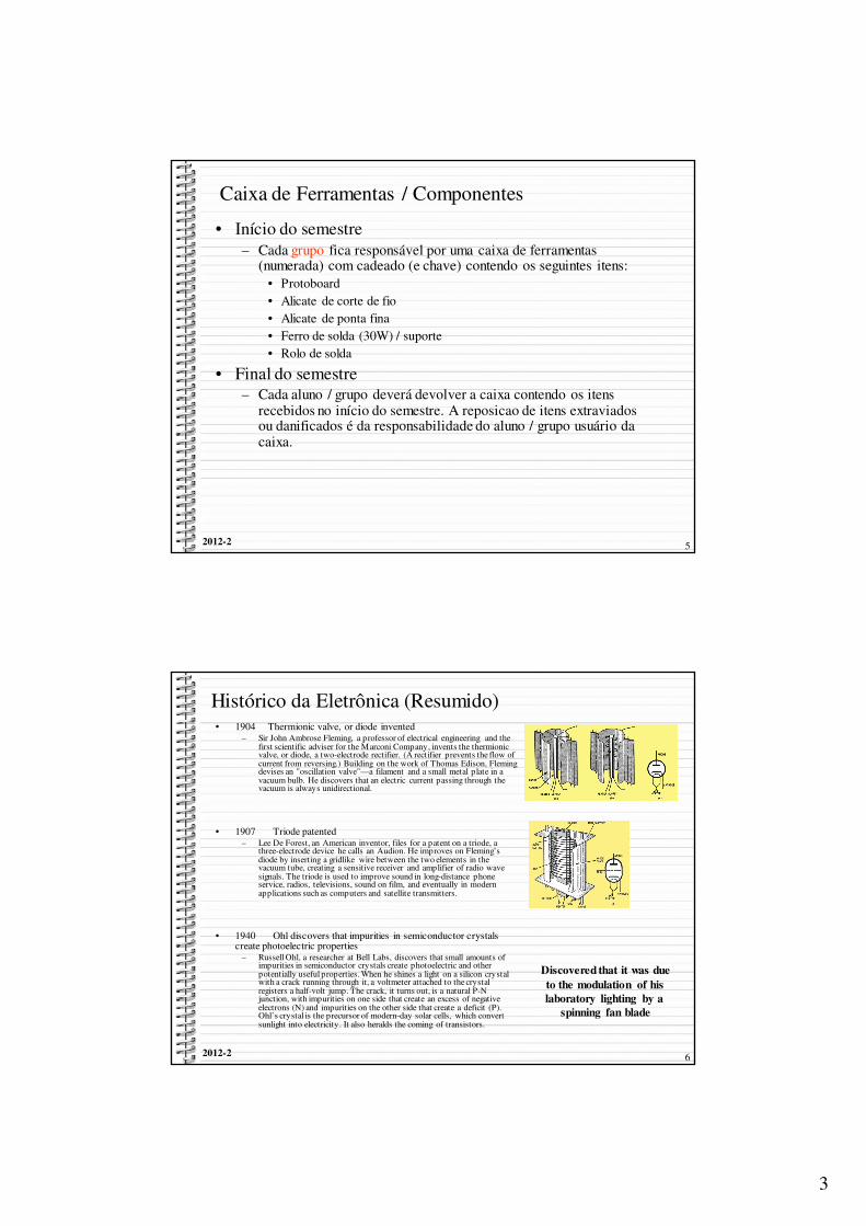
Caixa de Ferramentas / Componentes
• Início do semestre– Cada grupo fica responsável por uma caixa de ferramentas
(numerada) com cadeado (e chave) contendo os seguintes itens:• Protoboard• Alicate de corte de fio• Alicate de ponta fina• Ferro de solda (30W) / suporte• Rolo de solda
• Final do semestre– Cada aluno / grupo deverá devolver a caixa contendo os itens
recebidos no início do semestre. A reposicao de itens extraviados ou danificados é da responsabilidade do aluno / grupo usuário da caixa.
2012-2 6
Histórico da Eletrônica (Resumido)• 1904 Thermionic valve, or diode invented
– Sir John Ambrose Fleming, a professor of electrical engineering and the first scientific adviser for the Marconi Company, invents the thermionic valve, or diode, a two-electrode rectifier. (A rectifier prevents the flow of current from reversing.) Building on the work of Thomas Edison, Fleming devises an "oscillation valve"—a filament and a small metal plate in a vacuum bulb. He discovers that an electric current passing through the vacuum is always unidirectional.
• 1907 Triode patented– Lee De Forest, an American inventor, files for a patent on a triode, a
three-electrode device he calls an Audion. He improves on Fleming’s diode by inserting a gridlike wire between the two elements in the vacuum tube, creating a sensitive receiver and amplifier of radio wave signals. The triode is used to improve sound in long-distance phone service, radios, televisions, sound on film, and eventually in modern applications such as computers and satellite transmitters.
• 1940 Ohl discovers that impurities in semiconductor crystals create photoelectric properties
– Russell Ohl, a researcher at Bell Labs, discovers that small amounts of impurities in semiconductor crystals create photoelectric and other potentially useful properties. When he shines a light on a silicon crystal with a crack running through it, a voltmeter attached to the crystal registers a half-volt jump. The crack, it turns out, is a natural P-N junction, with impurities on one side that create an excess of negative electrons (N) and impurities on the other side that create a deficit (P). Ohl’s crystal is the precursor of modern-day solar cells, which convert sunlight into electricity. It also heralds the coming of transistors.
Discovered that it was due
to the modulation of his
laboratory lighting by a
spinning fan blade
4
2012-2 7
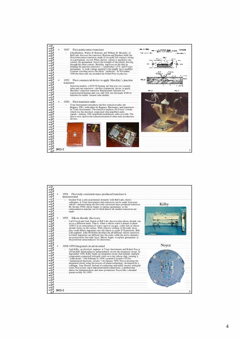
• 1947 First pointcontact transistor– John Bardeen, Walter H. Brattain, and William B. Shockley of
Bell Labs discover the transistor. Brattain and Bardeen build the first pointcontact transistor, made of two gold foil contacts sitting on a germanium crystal. When electric current is applied to one contact, the germanium boosts the strength of the current flowing through the other contact. Shockley improves on the idea by building the junction transistor—"sandwiches" of N- and P-type germanium. A weak voltage applied to the middle layer modifies a current traveling across the entire "sandwich." In November 1956 the three men are awarded the Nobel Prize in physics.
• 1952 First commercial device to apply Shockley’s junction transistor
– Sonotone markets a $229.50 hearing aid that uses two vacuum tubes and one transistor—the first commercial device to apply Shockley’s junction transistor. Replacement batteries for transistorized hearing aids cost only $10, not the nearly $100 of batteries for earlier vacuum tube models.
• 1954 First transistor radio– Texas Instruments introduces the first transistor radio, the
Regency TR1, with radios by Regency Electronics and transistors by Texas Instruments. The transistor replaces De Forest’s triode, which was the electrical component that amplified audio signals—making AM (amplitude modulation) radio possible. The door is now open to the transistorization of other mass production devices.
2012-2 8
• 1954 First truly consistent mass-produced transistor is demonstrated
– Gordon Teal, a physical chemist formerly with Bell Labs, shows colleagues at Texas Instruments that transistors can be made from pure silicon—demonstrating the first truly consistent mass-produced transistor. By the late 1950s silicon begins to replace germanium as the semiconductor material out of which almost all modern transistors are made.
• 1955 Silicon dioxide discovery– Carl Frosch and Link Derick at Bell Labs discover that silicon dioxide can
act as a diffusion mask. That is, when a silicon wafer is heated to about 1200°C in an atmosphere of water vapor or oxygen, a thin skin of silicon dioxide forms on the surface. With selective etching of the oxide layer, they could diffuse impurities into the silicon to create P-N junctions. Bell Labs engineer John Moll then develops the all-diffused silicon transistor, in which impurities are diffused into the wafer while the active elements are protected by the oxide layer. Silicon begins to replace germanium as the preferred semiconductor for electronics.
• 1958-1959 Integrated circuit invented– Jack Kilby, an electrical engineer at Texas Instruments and Robert Noyce
of Fairchild Semiconductor independently invent the integrated circuit. In September 1958, Kilby builds an integrated circuit that includes multiple components connected with gold wires on a tiny silicon chip, creating a "solid circuit." (On February 6, 1959, a patent is issued to TI for "miniaturized electronic circuits.") In January 1959, Noyce develops his integrated circuit using the process of planar technology, developed by a colleague, Jean Hoerni. Instead of connecting individual circuits with gold wires, Noyce uses vapor-deposited metal connections, a method that allows for miniaturization and mass production. Noyce files a detailed patent on July 30, 1959.
Kilby
Noyce
5
2012-2 9
• 1962 MOSFET is invented– The metal oxide semiconductor field effect transistor
(MOSFET) is invented by engineers Steven Hofstein and Frederic Heiman at RCA's research laboratory in Princeton, New Jersey. Although slower than a bipolar junction transistor, a MOSFET is smaller and cheaper and uses less power, allowing greater numbers of transistors to be crammed together before a heat problem arises. Most microprocessors are made up of MOSFETs, which are also widely used in switching applications.
• 1965 Automatic adaptive equalizer invented by Robert Lucky
– The automatic adaptive equalizer is invented in 1965 at Bell Laboratories by electrical engineer Robert Lucky. Automatic equalizers correct distorted signals, greatly improving data performance and speed. All modems still use equalizers.
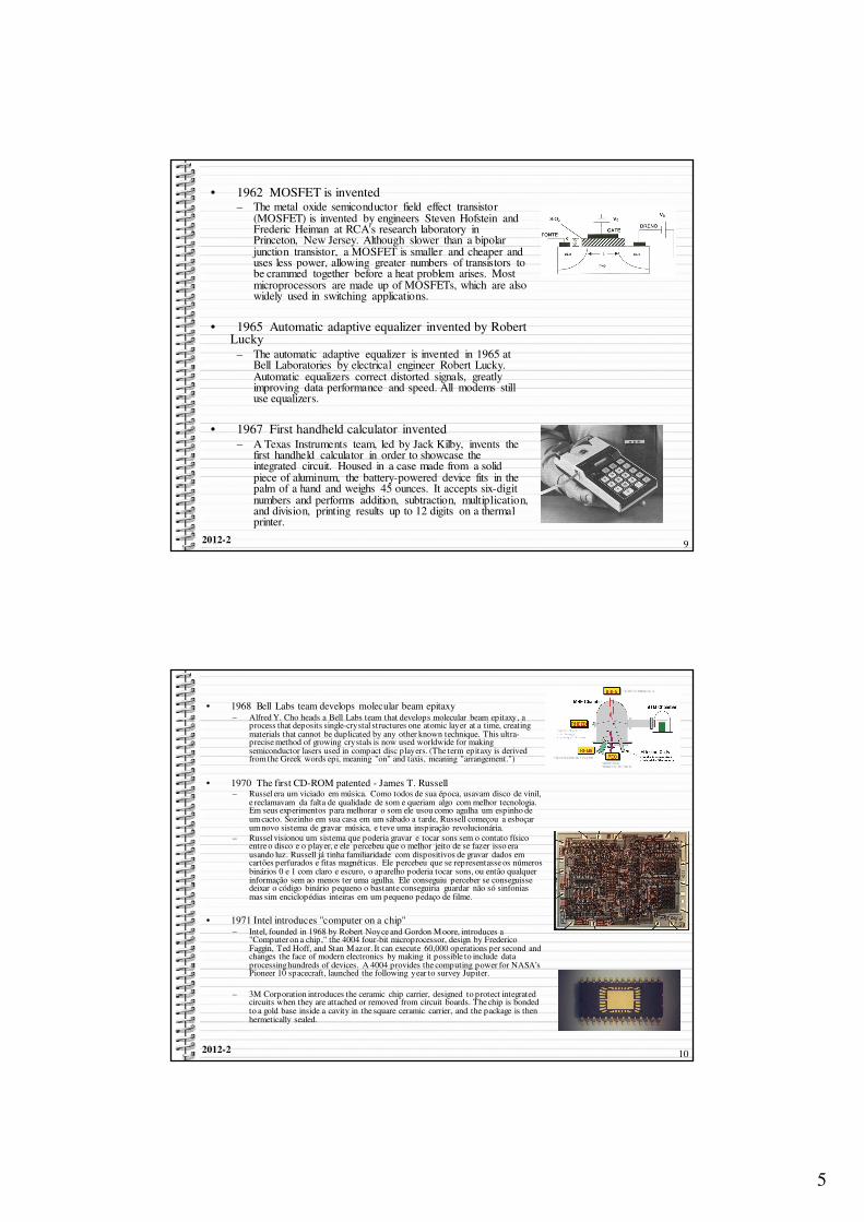
• 1967 First handheld calculator invented– A Texas Instruments team, led by Jack Kilby, invents the
first handheld calculator in order to showcase the integrated circuit. Housed in a case made from a solid piece of aluminum, the battery-powered device fits in the palm of a hand and weighs 45 ounces. It accepts six-digit numbers and performs addition, subtraction, multiplication, and division, printing results up to 12 digits on a thermal printer.
2012-2 10
• 1968 Bell Labs team develops molecular beam epitaxy– Alfred Y. Cho heads a Bell Labs team that develops molecular beam epitaxy, a
process that deposits single-crystal structures one atomic layer at a time, creating materials that cannot be duplicated by any other known technique. This ultra-precise method of growing crystals is now used worldwide for making semiconductor lasers used in compact disc players. (The term epitaxy is derived from the Greek words epi, meaning "on" and taxis, meaning "arrangement.")
• 1970 The first CD-ROM patented - James T. Russell– Russel era um viciado em música. Como todos de sua época, usavam disco de vinil,
e reclamavam da falta de qualidade de som e queriam algo com melhor tecnologia. Em seus experimentos para melhorar o som ele usou como agulha um espinho de um cacto. Sozinho em sua casa em um sábado a tarde, Russell começou a esboçar um novo sistema de gravar música, e teve uma inspiração revolucionária.
– Russel visionou um sistema que poderia gravar e tocar sons sem o contato físico entre o disco e o player, e ele percebeu que o melhor jeito de se fazer isso era usando luz. Russell já tinha familiaridade com dispositivos de gravar dados em cartões perfurados e fitas magnéticas. Ele percebeu que se representasse os números binários 0 e 1 com claro e escuro, o aparelho poderia tocar sons, ou então qualquer informação sem ao menos ter uma agulha. Ele conseguiu perceber se conseguisse deixar o código binário pequeno o bastante conseguiria guardar não só sinfonias mas sim enciclopédias inteiras em um pequeno pedaço de filme.
• 1971 Intel introduces "computer on a chip"– Intel, founded in 1968 by Robert Noyce and Gordon Moore, introduces a
"Computer on a chip," the 4004 four-bit microprocessor, design by Frederico Faggin, Ted Hoff, and Stan Mazor. It can execute 60,000 operations per second and changes the face of modern electronics by making it possible to include data processing hundreds of devices. A 4004 provides the computing power for NASA's Pioneer 10 spacecraft, launched the following year to survey Jupiter.
– 3M Corporation introduces the ceramic chip carrier, designed to protect integrated circuits when they are attached or removed from circuit boards. The chip is bonded to a gold base inside a cavity in the square ceramic carrier, and the package is then hermetically sealed.
6
2012-2 11
• 1972 Home video game systems become available– In September, Magnavox ships Odyssey 100 home game
systems to distributors. The system is test marketed in 25 cities, and 9,000 units are sold in Southern California Alone during the first month at a price of $99.95.
– In November, Nolan Bushnell forms Atari and ships Pong, a coin-operated video arcade game, designed and built by Al Alcorn. The following year Atari introduces its home version of the game, which soon outstrips Odyssey 100.
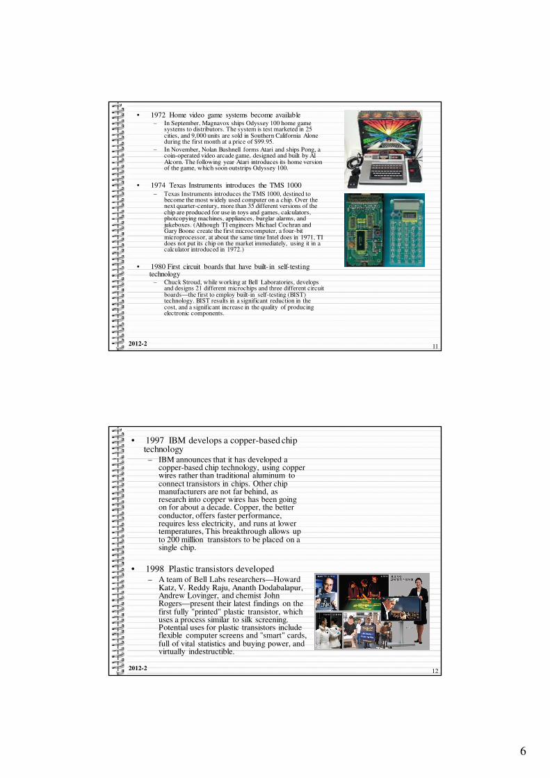
• 1974 Texas Instruments introduces the TMS 1000– Texas Instruments introduces the TMS 1000, destined to
become the most widely used computer on a chip. Over the next quarter-century, more than 35 different versions of the chip are produced for use in toys and games, calculators, photcopying machines, appliances, burglar alarms, and jukeboxes. (Although TI engineers Michael Cochran and Gary Boone create the first microcomputer, a four-bit microprocessor, at about the same time Intel does in 1971, TI does not put its chip on the market immediately, using it in a calculator introduced in 1972.)
• 1980 First circuit boards that have built- in self-testing technology
– Chuck Stroud, while working at Bell Laboratories, develops and designs 21 different microchips and three different circuit boards—the first to employ built-in self-testing (BIST) technology. BIST results in a significant reduction in the cost, and a significant increase in the quality of producing electronic components.
2012-2 12
• 1997 IBM develops a copper-based chip technology– IBM announces that it has developed a
copper-based chip technology, using copper wires rather than traditional aluminum to connect transistors in chips. Other chip manufacturers are not far behind, as research into copper wires has been going on for about a decade. Copper, the better conductor, offers faster performance, requires less electricity, and runs at lower temperatures, This breakthrough allows up to 200 million transistors to be placed on a single chip.
• 1998 Plastic transistors developed– A team of Bell Labs researchers—Howard
Katz, V. Reddy Raju, Ananth Dodabalapur, Andrew Lovinger, and chemist John Rogers—present their latest findings on the first fully "printed" plastic transistor, which uses a process similar to silk screening. Potential uses for plastic transistors include flexible computer screens and "smart" cards, full of vital statistics and buying power, and virtually indestructible.
7
2012-2 13
Definições em Eletrônica
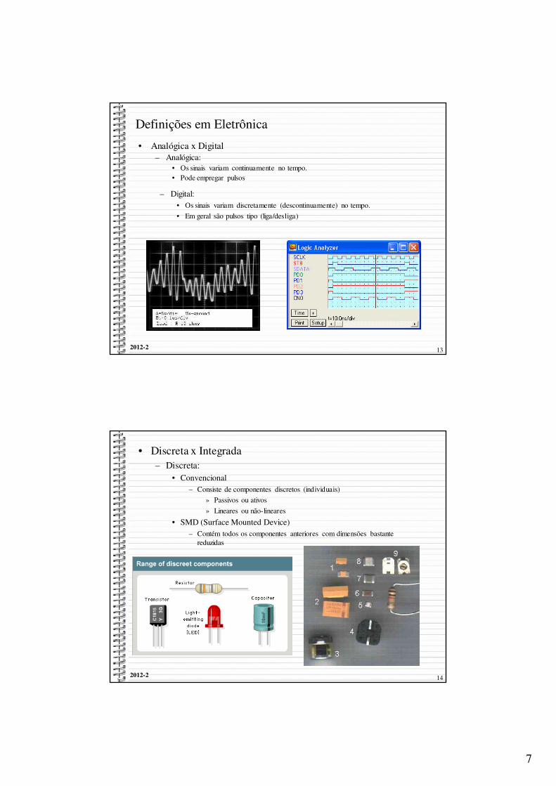
• Analógica x Digital– Analógica:
• Os sinais variam continuamente no tempo.• Pode empregar pulsos
– Digital: • Os sinais variam discretamente (descontinuamente) no tempo.
• Em geral são pulsos tipo (liga/desliga)
2012-2 14
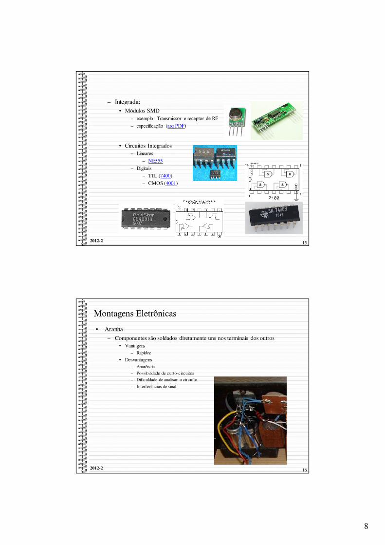
• Discreta x Integrada– Discreta:
• Convencional– Consiste de componentes discretos (individuais)
» Passivos ou ativos
» Lineares ou não-lineares
• SMD (Surface Mounted Device)– Contém todos os componentes anteriores com dimensões bastante
reduzidas
8
2012-2 15
– Integrada:• Módulos SMD
– exemplo: Transmissor e receptor de RF
– especificação (arq PDF)
• Circuitos Integrados– Lineares
– NE555
– Digitais
– TTL (7400)
– CMOS (4001)
2012-2 16
Montagens Eletrônicas
• Aranha– Componentes são soldados diretamente uns nos terminais dos outros
• Vantagens– Rapidez
• Desvantagens– Aparência
– Possibilidade de curto-circuitos
– Dificuldade de analisar o circuíto
– Interferências de sinal
9
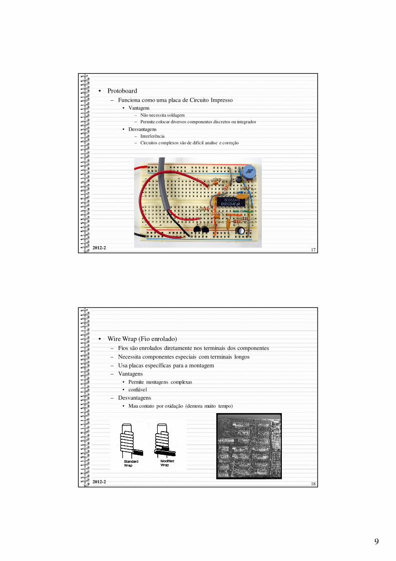
2012-2 17
• Protoboard– Funciona como uma placa de Circuito Impresso
• Vantagens– Não necessita soldagem
– Permite colocar diversos componentes discretos ou integrados
• Desvantagens– Interferência
– Circuitos complexos são de difícil analise e correção
2012-2 18
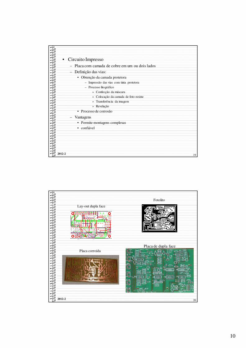
• Wire Wrap (Fio enrolado)– Fios são enrolados diretamente nos terminais dos componentes
– Necessita componentes especiais com terminais longos
– Usa placas específicas para a montagem
– Vantagens• Permite montagens complexas
• confiável
– Desvantagens• Mau contato por oxidação (demora muito tempo)
10
2012-2 19
• Circuito Impresso– Placa com camada de cobre em um ou dois lados
– Definição das vias:• Obtenção da camada protetora
– Impressão das vias com tinta protetora
– Processo litográfico
» Confecção da máscara
» Colocação da camada de foto-resiste
» Transferência da imagem
» Revelação
• Processo de corrosão
– Vantagens• Permite montagens complexas
• confiável
2012-2 20
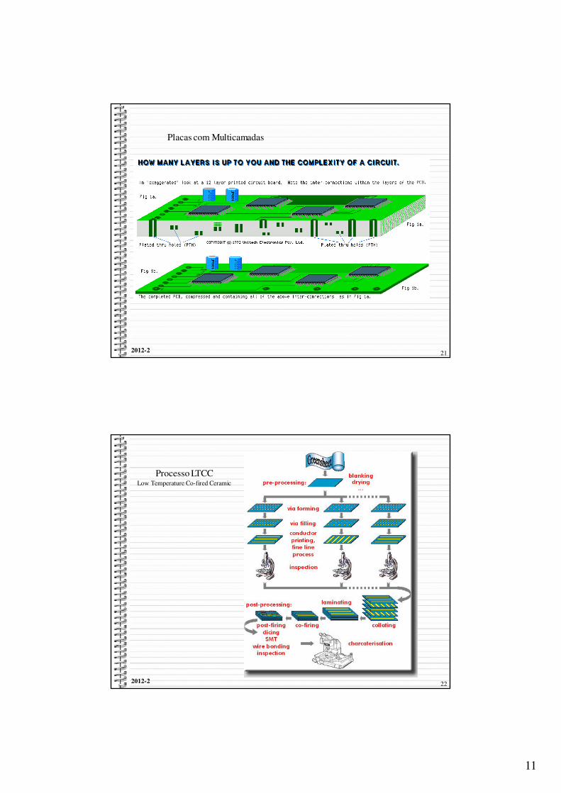
Placa corroída
Fotolito
Placa de dupla face
Lay-out dupla face
11
2012-2 21
Placas com Multicamadas
2012-2 22
Processo LTCCLow Temperature Co-fired Ceramic
12
2012-2 23
Necessidade de Miniaturização
• After Spielberg, S. “1941” (1979)
2012-2 24
Efeitos Macro de Forças Micro
• Processo de deslocamento de Laragtixas em paredes– Forças de Van der Waals promovem a adesão
13
2012-2 25
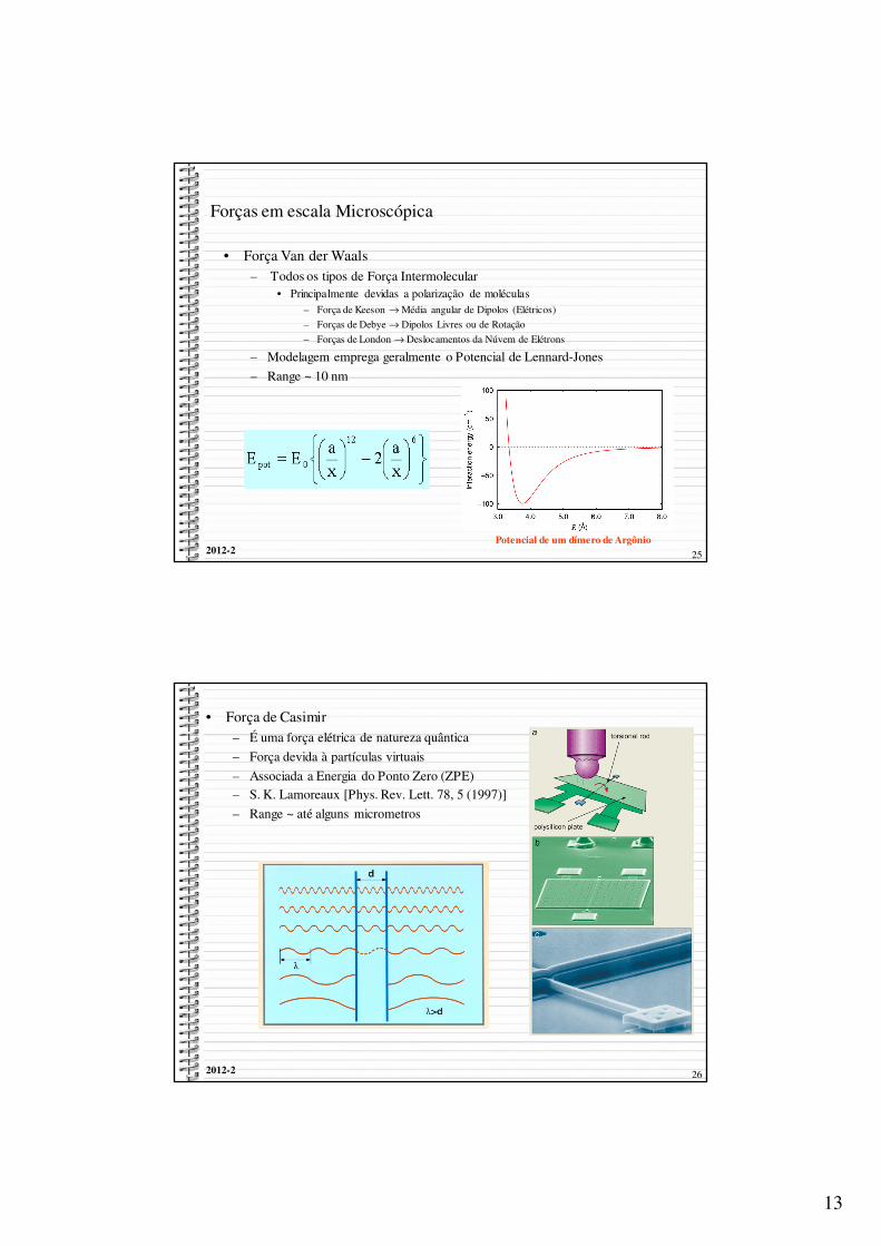
Forças em escala Microscópica
• Força Van der Waals – Todos os tipos de Força Intermolecular
• Principalmente devidas a polarização de moléculas– Força de Keeson → Média angular de Dipolos (Elétricos)
– Forças de Debye → Dipolos Livres ou de Rotação
– Forças de London → Deslocamentos da Núvem de Elétrons
– Modelagem emprega geralmente o Potencial de Lennard-Jones
– Range ~ 10 nm
Potencial de um dímero de Argônio
2012-2 26
• Força de Casimir– É uma força elétrica de natureza quântica
– Força devida à partículas virtuais
– Associada a Energia do Ponto Zero (ZPE)
– S. K. Lamoreaux [Phys. Rev. Lett. 78, 5 (1997)]
– Range ~ até alguns micrometros
14
2012-2 27
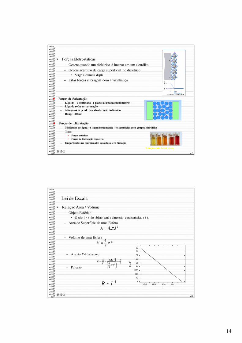
• Forças Eletrostáticas– Ocorre quando um dielétrico é imerso em um eletrólito
– Ocorre acúmulo de carga superficial no dielétrico• Surge a camada dupla
– Estas forças interagem com a vizinhança
� Forças de Solvatação
– Líquido →→→→ confinado →→→→ placas afastadas nanômetros
– Líquido sofre estruturação
– A força →→→→ depende da estruturação do líquido
– Range ~10 nm
� Forças de Hidratação
– Moléculas de água →→→→ ligam fortemente →→→→ superfícies com grupos hidrófilos
– Tipos
• Forças estéricas
• Forças de hidratação repulsiva
– Importantes na química dos colóides e em biologia
Soluções coloidais de AuAg
2012-2 28
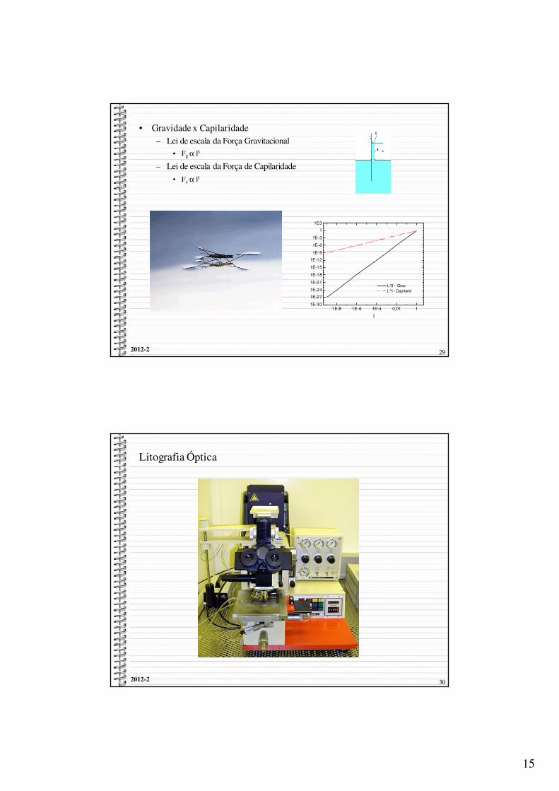
• Relação Área / Volume– Objeto Esférico
• O raio ( r ) do objeto será a dimensão característica ( l ).
– Área de Superfície de uma Esfera
– Volume de uma Esfera
2..4 lA π=
3..3
4lV π=
– A razão R é dada por:
– Portanto
( )l
l
l
V
AR
3
..3
4..4
3
2
=
==
π
π
1~ −lR 1E-8 1E-6 1E-4 0,01 1
1
10
100
1000
1E4
1E5
1E6
1E7
1E8
1E9
R α
l-1
l
Lei de Escala
15
2012-2 29
• Gravidade x Capilaridade– Lei de escala da Força Gravitacional
• Fg α l3
– Lei de escala da Força de Capilaridade
• Fc α l1
1E-8 1E-6 1E-4 0,01 11E-30
1E-27
1E-24
1E-21
1E-18
1E-15
1E-12
1E-9
1E-6
1E-3
1
1E3
L 3̂ - Grav
L 1̂- Capilarid
l
2012-2 30
Litografia Óptica
16
2012-2 31
• Positive Resist Process– Shipley S1400-27
• Negative Resist Process– Futurrex NR8-1000
Si wafer
Glass Mask
UV - Light
Pattern
Resist removed during development
Resist NOT removed during development
UV Light breaks chemical bonds in the
resist polymer making it soluble
Si wafer
Glass Mask
UV - Light
Pattern
Resist removed during development
Resist NOT removed during development
UV Light activates chemical reactions of polymerization
turning the resist insoluble.
2012-2 32
Resist removed during development
Resist NOT removed during development
Si wafer
Glass Mask
UV - Light
Pattern
Under-etch occurs during thedevelopment processing
Lift-off Profile for Negative Resist
• Positive Resist Process– Shipley S1813– Wafer drying – Hot plate 90oC / 2 min– Spin Coat 5000 RPM / 30s → 1,2 µm– Soft-bake 90 / 1 min– Chlorobenzene Soak 10 min (hardens surface)– Exposition 70 mJ/cm2 (necessary)– Development– Post-bake 100oC / 2 min
17
2012-2 33
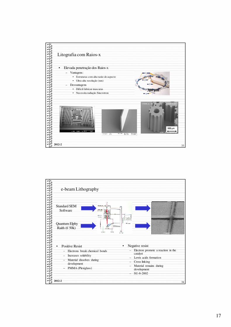
Litografia com Raios-x
• Elevada penetração dos Raios-x– Vantagens:
• Estruturas com alta razão de aspecto
• Ultra-alta resolução (nm)
– Desvantagens• Difícil fabricar mascaras
• Necessita radiação Sincrotron300 µm
2012-2 34
e-beam Lithography
• Positive Resist– Electrons break chemical bonds
– Increases solubility
– Material dissolves during development
– PMMA (Plexiglass)
• Negative resist– Electron promote a reaction in the
catalyst– Lewis acids formation– Cross linking– Material remains during
development– SU-8-2002
Standard SEMSoftware
Quantum ElphyRaith (€ 50k)
18
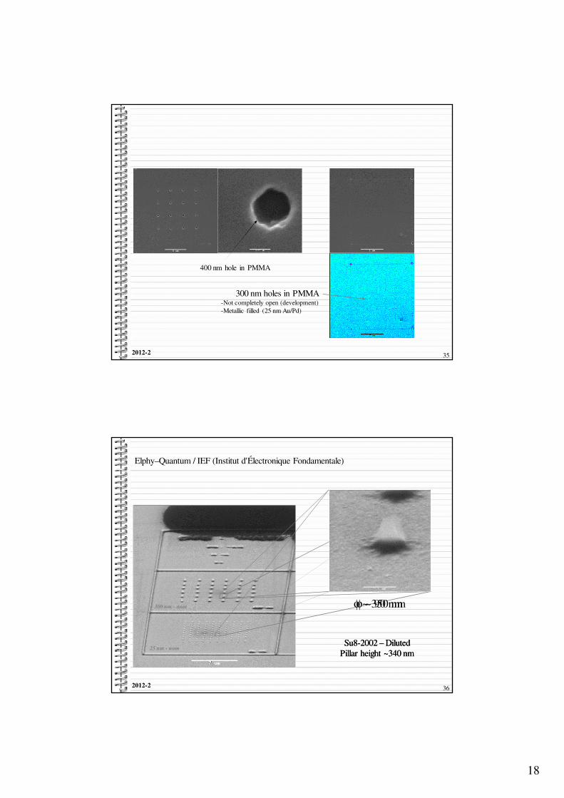
2012-2 35
400 nm hole in PMMA
300 nm holes in PMMA-Not completely open (development)-Metallic filled (25 nm Au/Pd)
2012-2 36
φ ~ 90 nm
Elphy–Quantum / IEF (Institut d'Électronique Fondamentale)
Su8Su8--2002 2002 –– DilutedDilutedPillar height ~340 nmPillar height ~340 nm
25 nm - nom
300 nm - nom φ ~ 350 nm
19
2012-2 37
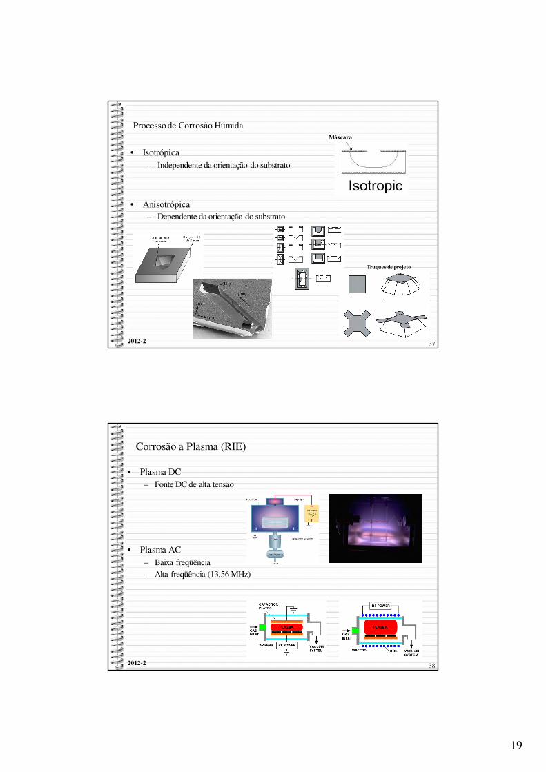
Processo de Corrosão Húmida
• Isotrópica– Independente da orientação do substrato
• Anisotrópica– Dependente da orientação do substrato
Máscara
Truques de projeto
2012-2 38
Corrosão a Plasma (RIE)
• Plasma DC– Fonte DC de alta tensão
• Plasma AC– Baixa freqüência– Alta freqüência (13,56 MHz)
20
2012-2 39
2012-2 40
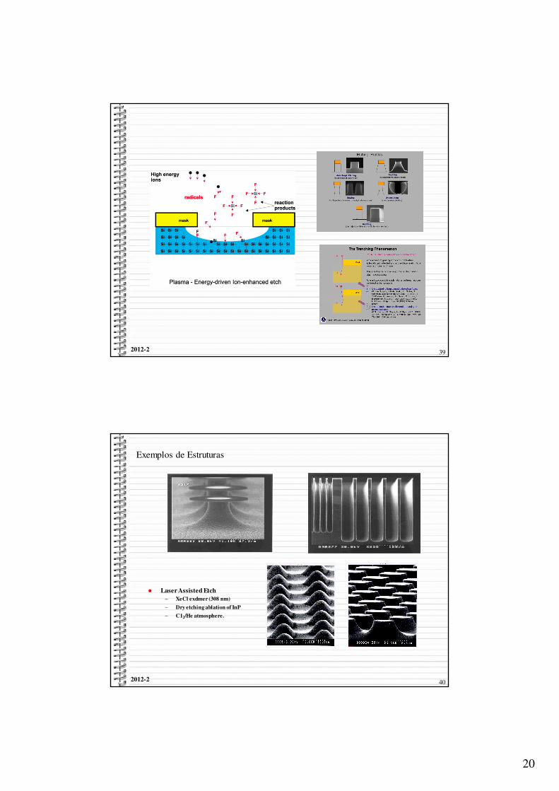
Exemplos de Estruturas
� Laser Assisted Etch
– XeCl exdmer (308 nm)
– Dry etching ablation of InP
– C12/He atmosphere.
21
2012-2 41
Oxidação de Silício
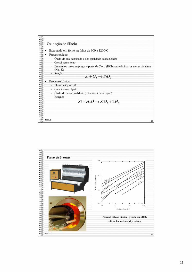
• Executada em forno na faixa de 900 a 1200oC• Processo Seco
– Óxido de alta densidade e alta qualidade (Gate Oxide)– Crescimento lento– Em muitos casos emprega vapores de Cloro (HCl) para eliminar os metais alcalinos
(Na , K)– Reação:
• Processo Úmido– Fluxo de O2 + H20– Crescimento rápido– Óxido de baixa qualidade (máscaras / passivação)– Reação:
2 2Si O SiO+ →
2 2 22Si H O SiO H+ → +
2012-2 42
Forno de 3-zonas
Thermal silicon dioxide growth on <100>
silicon for wet and dry oxides.
22
2012-2 43
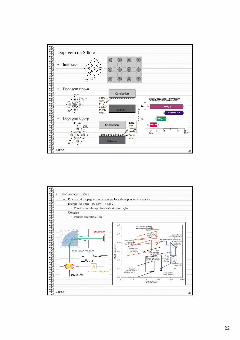
Dopagem de Silício
• Intrínseco
• Dopagem tipo-n
• Dopagem tipo-p
2012-2 44
• Implantação Iônica– Processo de dopagem que emprega Ions da impureza acelerados
– Energia do Feixe (10 keV – 6 MeV)• Permite controlar a profundidade de penetração
– Corrente• Permite controlar a Dose
23
2012-2 45
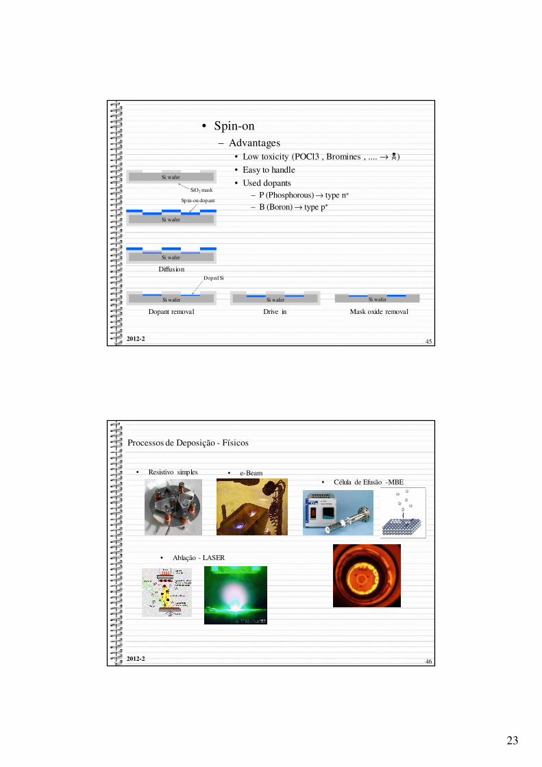
Si wafer
• Spin-on– Advantages
• Low toxicity (POCl3 , Bromines , .... → �)
• Easy to handle
• Used dopants – P (Phosphorous) → type n+
– B (Boron) → type p+
Si wafer
SiO2 mask
Si wafer
Spin-on dopant
Si wafer
Diffusion
Drive inDopant removal
Si wafer
Doped Si
Mask oxide removal
Si wafer
2012-2 46
Processos de Deposição - Físicos
• Resistivo simples • e-Beam• Célula de Efusão -MBE
• Ablação - LASER
24
2012-2 47
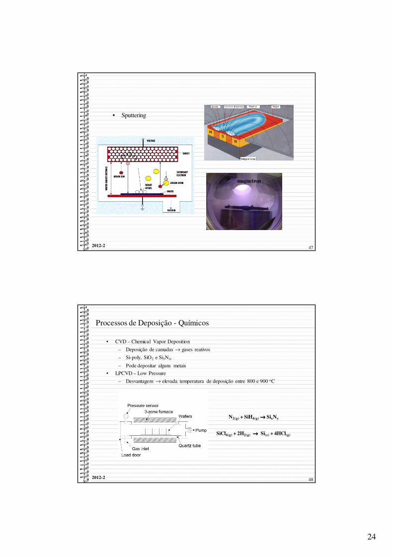
• Sputtering
magnetron
2012-2 48
Processos de Deposição - Químicos
• CVD – Chemical Vapor Deposition
– Deposição de camadas → gases reativos
– Si-poly, SiO2 e Si3N4.
– Pode depositar alguns metais
• LPCVD – Low Pressure
– Desvantagem → elevada temperatura de deposição entre 800 e 900 oC
N2(g) + SiH4(g) →→→→ SixNy
SiCl4(g) + 2H2(g) →→→→ Si(s) + 4HCl(g)
25
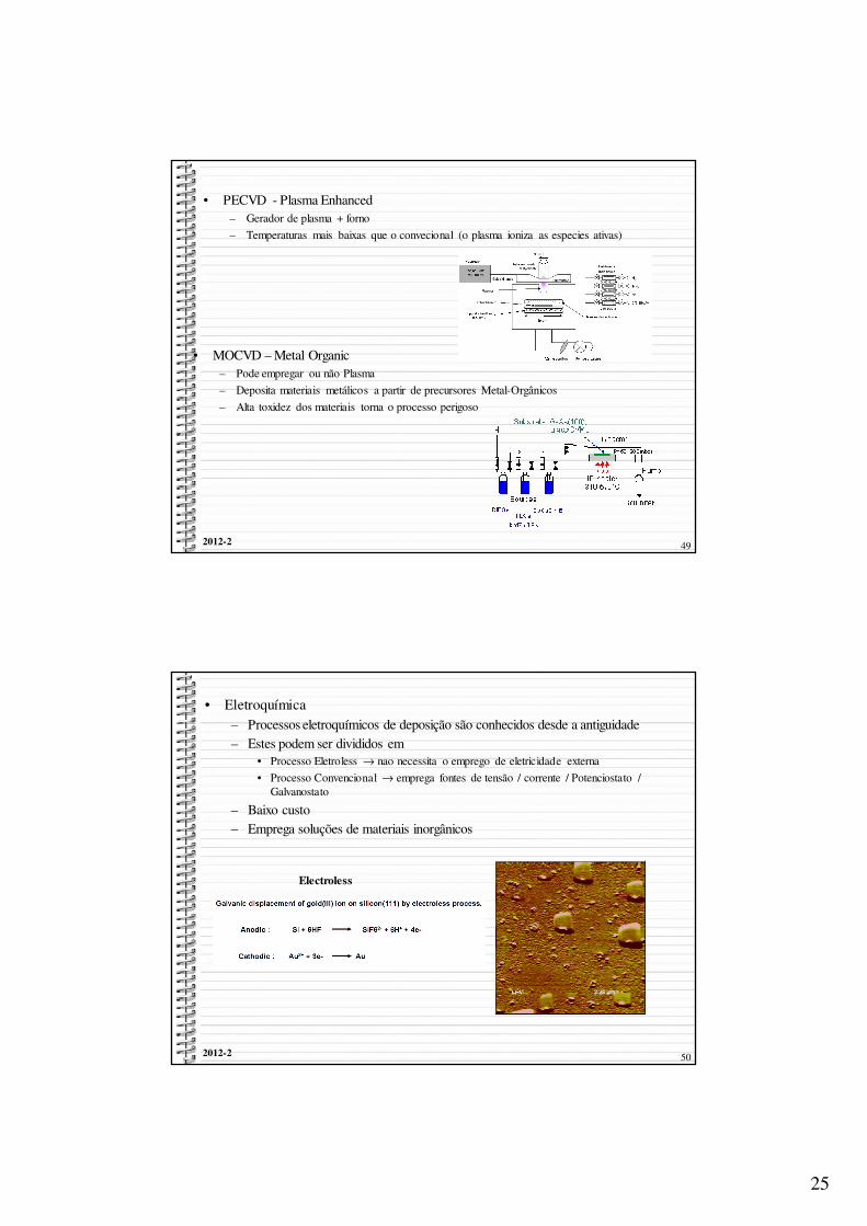
2012-2 49
• PECVD - Plasma Enhanced – Gerador de plasma + forno
– Temperaturas mais baixas que o convecional (o plasma ioniza as especies ativas)
• MOCVD – Metal Organic – Pode empregar ou não Plasma
– Deposita materiais metálicos a partir de precursores Metal-Orgânicos
– Alta toxidez dos materiais torna o processo perigoso
2012-2 50
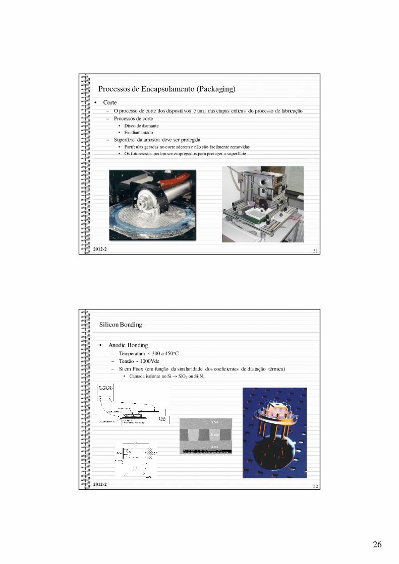
• Eletroquímica– Processos eletroquímicos de deposição são conhecidos desde a antiguidade– Estes podem ser divididos em
• Processo Eletroless → nao necessita o emprego de eletricidade externa
• Processo Convencional → emprega fontes de tensão / corrente / Potenciostato / Galvanostato
– Baixo custo– Emprega soluções de materiais inorgânicos
Electroless
26
2012-2 51
Processos de Encapsulamento (Packaging)
• Corte– O processo de corte dos dispositivos é uma das etapas críticas do processo de fabricação
– Processos de corte• Disco de diamante
• Fio diamantado
– Superfície da amostra deve ser protegida• Partículas geradas no corte aderem e não são facilmente removidas
• Os fotoresistes podem ser empregados para proteger a superfície
2012-2 52
Silicon Bonding
• Anodic Bonding– Temperatura ~ 300 a 450oC
– Tensão ~ 1000Vdc
– Si em Pirex (em função da similaridade dos coeficientes de dilatação térmica)• Camada isolante no Si → SiO2 ou Si3N4
27
2012-2 53
• Soldagem de Fios– Wire bonding permite conectar os dispositivos microfabricados com a eletrônica
externa.– Em geral são empregados fios de Au ou Al– O processo de soldagem envolve
• Pressão mecânica
• Vibração ultra-sônica
2012-2 54
28
2012-2 55
FIM