ce3411 microprocessor systems lab...8255a interface (7-segment) objective: to get familiar with the...
TRANSCRIPT
CE3411 MICROPROCESSOR SYSTEMS LAB
Kingdom of Saudi Arabia
Ministry of Education Prince Sattam Bin Abdulaziz University College of Computer Engineering & Sciences
Department of Computer Engineering
اململكة العربية الصعودية
وزارة التعليم
جامعة األمري شطام بن عبدالعسيس
م احلاشبكلية هندشة وعلو
قصم هندشة احلاشب

Laboratory Safety :
Please read these Safety Guidelines, Safety is a priority at Prince Sattam Bin Abdulaziz
University .While it may seem unlikely that an accident could happen to you, you
should know the accident rate in universities is 10 to 100 times greater than in the
chemical industry. To help prevent accidents, safety notes are included in the lab
manual. In addition, any relevant Material Safety Data Sheets (MSDS) are posted in a
laboratory binder and guidelines.
Pay close attention to this information – our goals are:
1. To avoid accidents in the lab, and
2. To respond promptly and appropriately should an accident occur.
Safety depends on you!
It is your responsibility to follow the instructions in the
lab manual and any additional guidelines provided by
your instructor. It is also your responsibility to be
familiar with the location and operation of safety
equipment.

General Laboratory Safety Guidelines
• Wear appropriate protective clothing. Do not wear open-toed shoes, sandals, shorts
or shirts with dangling sleeves. Tie back long hair and avoid dangling jewelry.
• Clean your workstation after each lab period, and return all equipment and
materials to appropriate stations before leaving the lab.
• Always turn off the power before working on any electric circuit or electronic device.
• When operating with electric circuits and electronic devices other than just a
computer, you must work in pairs or teams.
• When in doubt about the operation of any circuit or device in lab, always have an
instructor check your work before connecting power to your system.
• Report any safety issues or violations that you are aware of as soon as possible to
your course instructor and program director.
• Ensure that you have a safe buffer area around you and that you are working on
an appropriate surface when using soldering irons in the lab.
• Always make sure that all lab equipment, soldering irons, project circuits are
powered down before leaving your lab area.
• Ensure that your work environment is clear and free of debris before starting your
work AND after finishing your project.
• Never block walkways in the laboratory with lab equipment, cables, and electrical
power cords.
• Do not eat, drink, smoke, or apply cosmetics in the laboratory.
• Avoid all horseplay in the laboratory.
• Dispose of sharps waste properly — place broken glass in the glass discard container,
metal in the metal waste container, and place other waste materials in the designated
container(s). Secure all sharps, including needles, blades, probes, knives, etc.
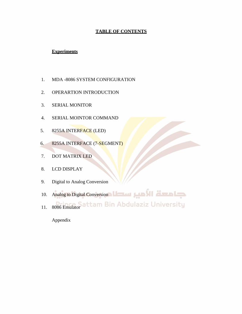
TABLE OF CONTENTS
Experiments
1.
MDA -8086 SYSTEM CONFIGURATION
2.
OPERARTION INTRODUCTION
3.
SERIAL MONITOR
4.
SERIAL MOINTOR COMMAND
5.
8255A INTERFACE (LED)
6.
8255A INTERFACE (7-SEGMENT)
7.
DOT MATRIX LED
8.
LCD DISPLAY
9.
Digital to Analog Conversion
10.
Analog to Digital Conversion
11.
8086 Emulator
Appendix

EXPERIMENT No.1
MDA -8086 SYSTEM CONFIGURATION
Objective:
To get familiar with the MDA-8086 kit and it components functions.
Equipment:
MDA-8086 kit.
Introduction:
MDA-8086 is kit having microprocessor and various other components for the detailed
understanding of 8086 microprocessor.
Components and Its Functions:
1-CPU (Central processing unit): Using Intel 8086, Using 4.9152 MHz
2-ROM (Read Only Memory):
It has program to control user's key inputs.
LCD display, user’s program. 64K Byte, it has data communication program.
Range o f ROM Address is F0000~FFFFFH.
3- SRAM (Static Random Access Memory):
Input user's program & data. Address of memory is 00000H~0FFFFH, totally 64K Byte.
4-DISPLAY:
It is LCD, 16(Character r) ×2(Line).
5- KEY BOARD: It is used to input machine language and has 16 of hexa-decimal keys and 8 of function
keys.
6- SPEAKER: Able to test so und using with speaker and further more able to test synthesizer.
7-RS-232C: It is ready to do data communication with IBM compatible personal computer.
8-DOT MATRIX LED: To understand & test of dot matrix structure and principle of display it is interfaced to
8255A (PPI).
9- A /D CONVERTER:
Convert analog signal to digital signal using with AD C0804.
10- D /A CONVERTER: Convert digital signal to analog signal using with D A C0800 and it is interfaced so as to
more Level meter.
11- STEPPING MOTOR INTERFACE:

So as to control stepping mo to r drive r circuit of stepping motor is interfaced.
12-POWER:
A C 110~220V, D C +5V 3A, +12V 1A, -12V 0.5A SMPS.
Memory Map:
Address Memory Description
00000H ~ 0FFFFH RAM PROGRAM & DATA MEMORY
F0000H ~ FFFFFH ROM MONITOR ROM
10000H ~ EFFFFH USER'S RANGE
I/O Address Map:
ADDRESS I/O PORT DESCRIPTION
00H ~ 07H LCD & KEYBOARD LCD Display
00H : INSTRUCTION REGISTER
02H : STATUS REGISTER
04H : DATA REGISTER
KEYBOARD
01H : KEYBOARD REGISTER (Only
read)
01H : KEYBOARD FLAG (Only
write)
08H ~ 0FH 8251 / 8253 8251(Using to data communication)
08H : DATA REGISTER
0AH : INSTRUCTION / STATUS
REGISTER
8253(TIMER/COUNTER)
09H : TIMER 0 REGISTER
0BH : TIMER 1 REGISTER
0DH : TIMER 2 REGISTER
0FH : CONTROL REGISTER
10H ~ 17H 8255A-CS1/
8255A-CS2
8255A-CS1(DOT & ADC
INTERFACE)
18H : A PORT DATA REGISTER
1AH : B PORT DATA REGISTER
1CH : C PORT CONTROL
REGISTER
8255-CS2(LED & STEPPING
MOTOR)
19H : A PORT DATA REGISTER
1BH : B PORT DATA REGISTER
1DH : C PORT CONTROL
REGISTER
1FH : CONTROL REGISTER
20H ~ 2FH I/O EXTEND CONNECTOR
30H ~ FFH USER'S RANGE

EXPERIMENT No.2
OPERARTION INTRODUCTION
Objective:
To get familiar with the MDA-8086 kit:
1-Function of Keys
2-Basic Operation
Equipment:
MDA-8086 kit.
Introduction:
Detailed knowledge of kind and function of keys and it basic operations.
1-KIND & FUNCTION OF KEYS:
MDA-8086 has high performance 64K-byte monitor program. It is designed
for easy function. After power is on, the monitor begins to work. In addition
to all the key function the monitor has a memory checking routine.
The following is a simple description of the key functions.
2-BASIC OPERATIONS:
On a power-up, following message will be displayed on a LCD.

Whenever RES is pressed, the display becomes FIGURE 1-1 and user can operate
keyboard only in this situation.


Quiz:
Q: Write the names of functions keys available on your kit (MDA 8086)

EXPERIMENT No.3
SERIAL MONITOR
Objective:
To get familiar how MDA-8086 kit can be connected to computer and do different
operations.
Equipment:
MDA-8086 kit and a PC having Intel microprocessor and WinnComm installed on PC.
Introduction:
Serial monitor is the basic monitor program to do data communicate between MDA-8086
and computer.
1. How to use serial monitor?
So as to use serial monitor, move jumper P1 which located on the PCB like
this.
2. HOW TO CONNET MDA-8086 TO YOUR PC:
The MDA-8086 is connected serially through COM port of PC and in the following way:
The connector of computer RS-232C is 9 pin and RS-232C of MDA-8086 is 9 pin, must
be connected

3. MDA-8086 INSTALLATION:
The MDA-8086 is installed by connecting it to PC having Intel microprocessor and these
two will be connected by third party software WinnComm.
4. SETUP THE CONFIGURATION OF “WinnComm”:
The data communication between MDA-8086 and computer, need fixing initial of
COMM. When you push F5 key, following is displayed and the step of fixing initial is
like
follow
When on a power-up, following message will be displayed. This message is displayed
only when on a power-up, and does not display when press RESET key
5. ASSEMBLING/COMPILING THE SOURCE CODE:
For assembling or compiling the source code first open the related source code and
assemble or compile it according to either it is in assembly or in C language.
So for assembly click on the ASM 8086 and for C click on C 8086 this will ABS
(absolute file).
6. DWONDLOAD AND EXECUTE THE SOURCE FILE:
When the ABS file is generated the press ‘L’ for the program to download and then press
F3 to send the file for execution and lastly press ’G’ to execute and display the

result.
Quiz:
Q:Which program is used fo serial communication between MDA8086 kit and your
system?

EXPERIMENT No.4
SERIAL MOINTOR COMMAND
Objective:
Knowledge of basic commands for memory modification and displays the modifications.
Equipment:
MDA-8086 kit and a PC having Intel microprocessor and WinnComm installed on PC.
Introduction:
These commands are to modify the memory elements and movement of blocks from one
address o another memory address.
1. MEMORY MODIFY COMMAND
2. MEMROY DISPLAY COMMAND:
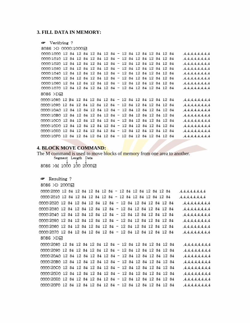
3. FILL DATA IN MEMORY:
4. BLOCK MOVE COMMAND:
The M command is used to move blocks of memory from one area to another.

5. DISPLAY REGISTER COMMAND:
The R command is used to display the i8086 processor registers.

6. TRACE COMMAND:
Executes instructions, one at a time, beginning at the location pointed to by the program
counter. After execution of each instruction, the processor registers are displayed
Quiz:
Q1: Which command is used for copying data from one memory location to another?
Q2: Which command is used to modify the memory elements ?
Q3: Which command is used to display the 8086 processor registers

EXPERIMENT No.5
8255A INTERFACE (LED)
Objective:
Glow of LEDS on the MDA-8086 kit using port B of PPI 8255.
Equipment:
PC having Intel microprocessor, MDA-8086 kit using WinnComm.
Introduction:
8255 is a programmable peripheral interface. It is compatible to Intel and other
microprocessors. It has 3 I/O ports named as port A, B, C and has 24 pins for I/O that are
programmable in group of 12 pins, has groups that operate in three distinct modes of
operation.
Interfacing of 8255A with 8086:

Quiz:
LED Glow Diagonally:
There are four leds on the kit which are connected to the port B (PB0-PB3) of 8255.
Write a code to make leds glow diagonally

EXPERIMENT No.6
8255A INTERFACE (7-SEGMENT)
Objective:
To get familiar with the seven segment display and its interfacing with 8086
microprocessor using 8255A.
Equipment:
PC having Intel microprocessor, MDA-8086 kit using WinnComm.
Introduction:
Seven segment is a display which may be either common anode or common cathode.
Which is ON either on 1 or zero but here we use the format ‘ON’ on zero (active low).
.
Interfacing of Seven segment with 8086 and 8255A:
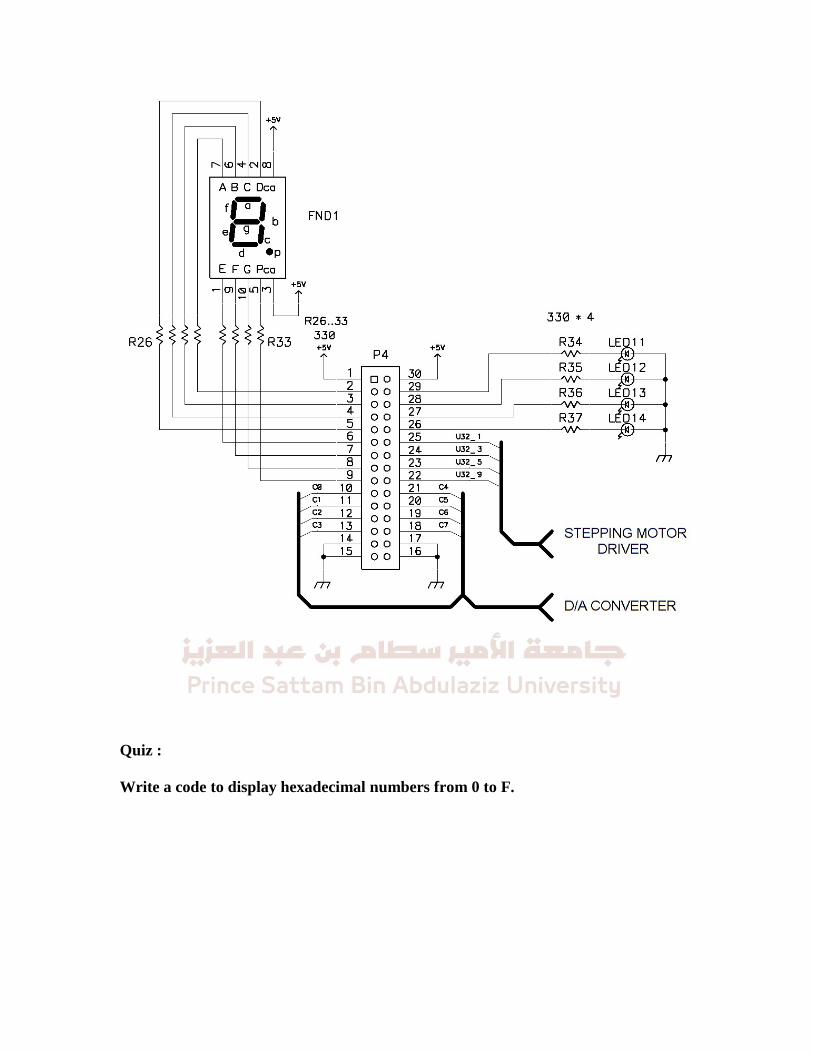
Quiz :
Write a code to display hexadecimal numbers from 0 to F.

EXPERIMENT No.7
DOT MATRIX LED
Objective:
To get familiar with dot matrix leds and their connections.
Equipment:
PC having Intel microprocessor, MDA-8086 kit using WinnComm.
1-DOT-MATRIX LED DISPLAY:
Introduction:
The KMD D1288C is 1.26 inch height 3mm diameter and 8 × 8 dot matrix LED displays.
The KMD D1288C are dual emitting color type of red, green chips are contained in a dot
with milky and white lens color. The dot matrix LEDs are active low.
Internal Circuit Diagram:
2-DOT-MATRIX LED INTERFACE:

Quiz:
1) Write a code to display letter “E” on dot matrix using red leds.
2) Write a code to display “KSA” on dot matrix using green leds.
3) Write a code to display a star on dot matrix.
EXPERIMENT No.8
LCD DISPLAY
Objective:
To get familiar with LCD its pin configuration, internal architecture and its interface with
PPI 8255A.
Equipment:
PC having Intel microprocessor, MDA-8086 kit using WinnComm.
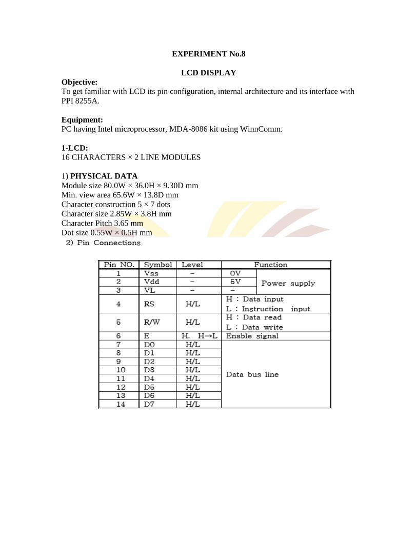
1-LCD:
16 CHARACTERS × 2 LINE MODULES
1) PHYSICAL DATA
Module size 80.0W × 36.0H × 9.30D mm
Min. view area 65.6W × 13.8D mm
Character construction 5 × 7 dots
Character size 2.85W × 3.8H mm
Character Pitch 3.65 mm
Dot size 0.55W × 0.5H mm

INSTRUCTIONS:

LCD INTERFACE:
The interface of LCD with 8255A is shown in the figure.
Quiz:
1) Write a code for displaying a sentence character by character.
2) Write a code of displaying your name and shifting towards right
3) Write a code of displaying your name and make the display on and off

EXPERIMENT No.9
Digital to Analog Conversion
Objective:
To get familiar with Digital to analog conversion
Equipment:
PC having Intel microprocessor, MDA 8086 kit
General Description:
The DAC0800 is a monolithic 8-Bit high-speed current output digital to analog converter
(DAC) featuring typical setting times of 100ns. When used as a multiplying DAC
monotonic performance over a 40 to 1 reference current range is possible.
Fig1:DAC0800 Block Diagram

D/A Converter Interface:

D/A Converter Experiment:
Setup jumper cap, like following;
Lab Task: When you send the Digital data to DAC then analog voltage will be
displayed on the LED Bar.
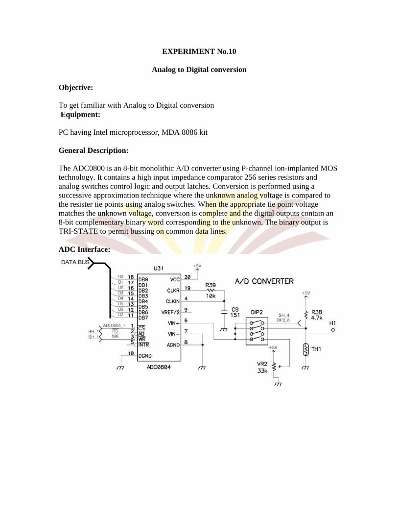
EXPERIMENT No.10
Analog to Digital conversion
Objective:
To get familiar with Analog to Digital conversion
Equipment:
PC having Intel microprocessor, MDA 8086 kit
General Description:
The ADC0800 is an 8-bit monolithic A/D converter using P-channel ion-implanted MOS
technology. It contains a high input impedance comparator 256 series resistors and
analog switches control logic and output latches. Conversion is performed using a
successive approximation technique where the unknown analog voltage is compared to
the resister tie points using analog switches. When the appropriate tie point voltage
matches the unknown voltage, conversion is complete and the digital outputs contain an
8-bit complementary binary word corresponding to the unknown. The binary output is
TRI-STATE to permit bussing on common data lines.
ADC Interface:

A/D Converter Experiment:
① Setting DIP2 switch on the left of ADC0804 like follow.
② Setup jumper cap, like following;
Lab Task: When you adjust the analog switches, ADC value will be displayed on the
LCD module.
EXPERIMENT No.11

8086 Emulator
Objective:
To get familiar with 8086 Emulator
Equipment:
PC having Intel microprocessor
Introduction:
This software is used for assembly programming.
Open the Emulator8086 from start menu.
Select new tab

Select option one and press ok.
Write your code in the highlighted area.

Compile your code.
Click on save.
Click on run button.
Following window will appear.
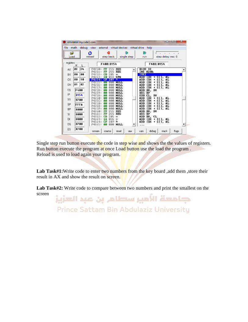
Single step run button execute the code in step wise and shows the the values of registers.
Run button execute the program at once Load button use the load the program .
Reload is used to load again your program.
Lab Task#1:Write code to enter two numbers from the key board ,add them ,store their
result in AX and show the result on screen.
Lab Task#2: Write code to compare between two numbers and print the smallest on the
screen

Appendix
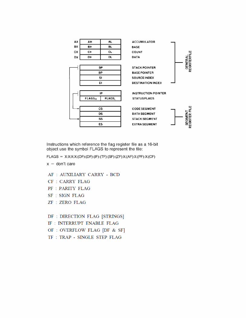
o 8086 Pin Configuration
o 8086 Register Model