consistent study of graphene structures through the direct
TRANSCRIPT
Consistent Study of Graphene Structures through the Direct Incorporation of Surface Conductivity
Georgios D. Bouzianas, Nikolaos V. Kantartzis, Traianos V. Yioultsis and Theodoros D. Tsiboukis Department of Electrical and Computer Engineering, Aristotle University of Thessaloniki, GR-54124 Thessaloniki, Greece
(email: [email protected], [email protected])
Basic Motives
GRAPHENE is the first truly two-dimensional (2-D) material to be observed and isolated in nature. In essence, it is a flat monolayer of carbon atoms tightly packed into a 2-D honeycomb lattice.
Its impressive electronic behavior is attributed to the fact that the energy-momentum relation for electrons is linear over a wide range of energies, rather than quadratic. Therefore, electrons act as massless relativistic particles, i.e. Dirac fermions.
Graphene has already found very interesting applications in the areas of integrated circuits and optoelectronics, while it is expected to be used in several devices from transformation optics, exploiting its capability to support the propagation of surface plasmonic waves.
Various techniques have been developed for the accurate simulation of graphene structures.
Objective: To enhance existing FDTD methods which use subcell techniques by directly incorporating the surface conductivity.
Graphene Conductivity Model
Simulation Results
Our study concentrates on the isotropic local conductivity case in the absence of an external magnetic field. The graphene surface conductivity is given by the Kubo formula.
The computational space was excited with a Total Field-Scattered Field formulation in conjunction with a near-to-far field transformation algorithm that was applied at surface S.
22
2 2 2 200
( ) ( ) ( 2 ) ( ) ( )( , , , )
( 2 ) ( 2 ) 4( / )d d d d
c
f f je j f fjeT d d
j j h
The first term resembles the intraband contributions, whereas the second term resembles the interband counterparts. We are interested in the intraband σintra term only, which is valid for microwave frequencies:
2
2
11
cintra
ej
µ τσ
ωτπ=
+
Generalized 3D FDTD Scheme
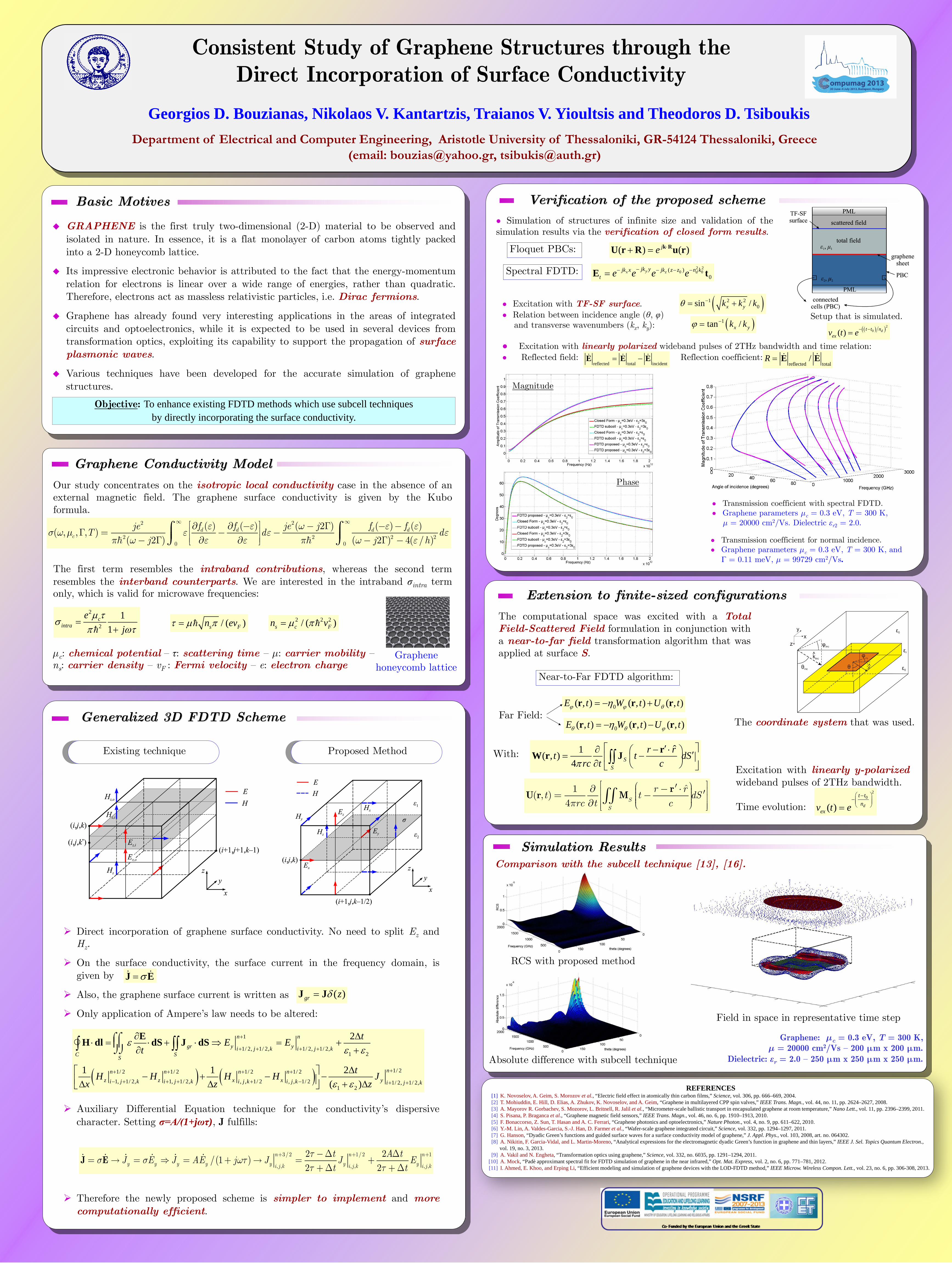
Graphene honeycomb lattice
Existing technique
Direct incorporation of graphene surface conductivity. No need to split Ez and Hz.
On the surface conductivity, the surface current in the frequency domain, is given by
Also, the graphene surface current is written as
Only application of Ampere’s law needs to be altered:
Auxiliary Differential Equation technique for the conductivity’s dispersive character. Setting σ=A/(1+jωτ), J fulfills:
3/2 1/2 1
, , , , , ,
2 2/ 1
2 2
n n n
y y y y y y yi j k i j k i j k
t AJ E J AE
tj J J E
t t
J E
( ) ( )
1
1/ 2, 1/ 2, 1/ 2, 1/ 2,1 2
1/ 21/ 2 1/ 2 1/ 2 1/ 2
1, 1/ 2, 1, 1/ 2, , , 1/ 2 , , 1/ 2 1/ 2, 1/ 2,1 2
2
1 1 2( )
n n
gr y yi j k i j kC SS
nn n n nz z x x yi j k i j k i j k i j k i j k
tE Et
tH H H H Jx z z
εε ε
ε ε
+
+ + + +
++ + + +
− + + + + − + +
∂ ∆⋅ = ⋅ + ⋅ ⇒ = +
∂ +
∆ − + − − ∆ ∆ + ∆
⌠⌠⌡⌡∫ ∫∫
EH dl dS J dS
Extension to finite-sized configurations
Far Field: 0( , ) ( , ) ( , )E t W t U tθ θ ϕη= − −r r r
0( , ) ( , ) ( , )E t W t U tϕ ϕ θη= − +r r r
Near-to-Far FDTD algorithm:
ˆ1( , )4 S
S
r rt t dSrc t cπ
′∂ − ⋅ ′= − ∂ ∫∫
rW r J
ˆ1( , )
4 S
S
r rt t dS
rc t c
rU r M
Comparison with the subcell technique [13], [16].
RCS with proposed method
Therefore the newly proposed scheme is simpler to implement and more computationally efficient.
μc: chemical potential – τ: scattering time – μ: carrier mobility – ns: carrier density – vF : Fermi velocity – e: electron charge
/ ( )s Fn evτ µ π=
2 2 2/ ( )s c Fn vµ π=
With:
Graphene: μc = 0.3 eV, T = 300 K, μ = 20000 cm2/Vs – 200 μm x 200 μm.
Dielectric: εr = 2.0 – 250 μm x 250 μm x 250 μm.
The coordinate system that was used.
Excitation with linearly y-polarized wideband pulses of 2THz bandwidth. Time evolution:
20
( ) d
t tn
exv t e −
− =
Field in space in representative time step
Absolute difference with subcell technique
( )gr zδ=J J
σ=J E
Proposed Method
• Simulation of structures of infinite size and validation of the simulation results via the verification of closed form results.
Verification of the proposed scheme
• Excitation with TF-SF surface. • Relation between incidence angle (θ, φ) and transverse wavenumbers (kx, ky):
2 20 0( )
0yx z djk yjk x jk z z n k
t e e e e−− − − −=E t
( ) ( )je ⋅+ = k RU r R u r
Spectral FDTD:
( )1 2 20sin /x yk k kθ −= +
( )1tan /x yk kϕ −=Setup that is simulated.
( )( )20( ) dt t nexv t e− −=
Floquet PBCs:
reflected total incident= −E E E
reflected total/R = E E
• Transmission coefficient for normal incidence. • Graphene parameters μc = 0.3 eV, T = 300 K, and Γ = 0.11 meV, μ = 99729 cm2/Vs.
Magnitude
Phase
• Transmission coefficient with spectral FDTD. • Graphene parameters μc = 0.3 eV, T = 300 K, μ = 20000 cm2/Vs. Dielectric εr2 = 2.0.
REFERENCES [1] K. Novoselov, A. Geim, S. Morozov et al., “Electric field effect in atomically thin carbon films,” Science, vol. 306, pp. 666–669, 2004. [2] T. Mohiuddin, E. Hill, D. Elias, A. Zhukov, K. Novoselov, and A. Geim, “Graphene in multilayered CPP spin valves,” IEEE Trans. Magn., vol. 44, no. 11, pp. 2624–2627, 2008. [3] A. Mayorov R. Gorbachev, S. Mozorov, L. Britnell, R. Jalil et al., “Micrometer-scale ballistic transport in encapsulated graphene at room temperature,” Nano Lett., vol. 11, pp. 2396–2399, 2011. [4] S. Pisana, P. Braganca et al., “Graphene magnetic field sensors,” IEEE Trans. Magn., vol. 46, no. 6, pp. 1910–1913, 2010. [5] F. Bonaccorso, Z. Sun, T. Hasan and A. C. Ferrari, “Graphene photonics and optoelectronics,” Nature Photon., vol. 4, no. 9, pp. 611–622, 2010. [6] Y.-M. Lin, A. Valdes-Garcia, S.-J. Han, D. Farmer et al., “Wafer-scale graphene integrated circuit,” Science, vol. 332, pp. 1294–1297, 2011. [7] G. Hanson, “Dyadic Green’s functions and guided surface waves for a surface conductivity model of graphene,” J. Appl. Phys., vol. 103, 2008, art. no. 064302. [8] A. Nikitin, F. Garcia-Vidal, and L. Martin-Moreno, “Analytical expressions for the electromagnetic dyadic Green’s function in graphene and thin layers,” IEEE J. Sel. Topics Quantum Electron., vol. 19, no. 3, 2013. [9] A. Vakil and N. Engheta, “Transformation optics using graphene,” Science, vol. 332, no. 6035, pp. 1291–1294, 2011. [10] A. Mock, “Padè approximant spectral fit for FDTD simulation of graphene in the near infrared,” Opt. Mat. Express, vol. 2, no. 6, pp. 771–781, 2012. [11] I. Ahmed, E. Khoo, and Erping Li, “Efficient modeling and simulation of graphene devices with the LOD-FDTD method,” IEEE Microw. Wireless Compon. Lett., vol. 23, no. 6, pp. 306-308, 2013.
• Excitation with linearly polarized wideband pulses of 2THz bandwidth and time relation: • Reflected field: Reflection coefficient: