design and implementation of a microcontroller … and implementation of a microcontroller based...
TRANSCRIPT

Al-Mansour Journal / Issue ( 24 ) 2015 ) 24(العدد /مجلة المنصور
- 19 -
Design and Implementation of a Microcontroller BasedDC/AC Inverter
Firas Mohammed Ali Al-Raie* Hawraa Qasim Hameed*
AbstractIn this paper, a method is proposed to improve the frequency stability and
accuracy of the generated wave in DC/AC square wave inverters using amicrocontroller-based stabilized oscillator circuit.The proposed technique relies on using the 8051 microcontroller as a
stable oscillator to generate two anti-phase 50 Hz square waves for thedriving power stage of the inverter based on a program stored in itsinternal ROM. These signals are then boosted to increase their voltageand current levels using BJT switching mode power transistors operatingin the push/pull mode. The resulting signal is then raised into the requiredvoltage level with the aid of a step-up transformer.A practical inverter circuit has been designed and constructed to convert
a 12 V battery DC input into 220 V AC output based on the 8051microcontroller. This circuit consists of an 8051 microcontroller, buffer,driver power transistor stage, final power transistor stage, and a step-uptransformer. The inverter circuit has been simulated, implemented, andtested practically. The test measurements have indicated that the circuitgives a full load power of 10 W with full-load voltage regulation of 8%, anda maximum conversion efficiency of 70%.
Keywords: DC/AC Inverter, Power Electronics, 8051 Microcontroller,Square Wave Inverter.
* Department of Electrical Engineering, University of Technology

Hawraa Qasim Hameed Firas Mohammed Ali Al-Raieحوراء قاسم حمید. م.، مفراس محمد علي.م.م
- 20 -
1. IntroductionAn inverter is an electronic circuit that converts direct current (DC) to
alternating current (AC) as shown in Figure 1.
Figure 1: Block Diagram of an Inverter.
Inverters are used in a wide range of applications, from small switchingpower supplies in computers, to large electric utility applications thattransport power, especially in renewable energy systems like solarsystems, wind power systems, …etc [1]. The inverter is so namedbecause it performs the opposite function of a rectifier. Most inverters dotheir job by performing two main functions: first they convert the incomingDC into AC, and then they step up the resulting AC to the required voltagelevel using a transformer. The most important parameters of the invertercircuit are its conversion power efficiency, frequency stability, outputvoltage regulation, and output waveform distortion [2].
Inverters can be classified into three types according to the shape of thegenerated waveform as depicted in Figure 2. These are the square waveinverters, modified sine wave inverters, and pure sine wave inverters.
Square wave inverters are simple in design and implementation. Theoutput voltage alternates between positive and negative values. Theoutput waveform, however, has a lot of amount of total harmonic distortion(THD) which results in a considerable power dissipation due to theseharmonics. On the other hand, the square wave inverter cannot regulateits AC output voltage when the battery voltage changes significantly. Thiscan cause some types of AC loads to fail suddenly [2].

Al-Mansour Journal / Issue ( 24 ) 2015 ) 24(العدد /مجلة المنصور
- 21 -
Figure 2: Types of the Generated Inverter Waveforms.
In the modified sine wave inverters, the output signal is similar to asquare wave except that it goes to zero for some delay time beforeswitching positively or negatively. This may reduce the THD, and givesbetter load compatibility. The shape of the waveform can also becontrolled to allow regulation of the AC output voltage level as thebattery’s voltage changes. The pulses of the square wave can be madetall and narrow when the battery voltage is high, and can be made shortand wide when the battery voltage is low. This results in a consistentaverage voltage for supplying the AC loads, and improves loadcompatibility and performance [3].Pure sine wave inverters produce a waveform that closely matches the
signal of the main power grid system. The generated waveform has verylow THD and thus these inverters can run more sensitive AC loads. Thedesign technique of pure sine inverters is complex and usually involvesthe use of PWM to produce hundreds of positive and negative pulsesduring each AC cycle. These pulses are then filtered into a smooth sinewave shape. Most true sine wave inverters are able to adjust the durationand timing of each pulse by using a microcontroller or microprocessorcontrol. This allows the voltage and frequency to be controlled to givebetter load compatibility and performance quality [4, 5].

Hawraa Qasim Hameed Firas Mohammed Ali Al-Raieحوراء قاسم حمید. م.، مفراس محمد علي.م.م
- 22 -
2. Square Wave DC/AC InvertersSimple types of square wave inverters consist of a square wave oscillator,
driver, power transistor switching circuit, and a transformer as shown inthe block diagram of Figure 3.
Figure 3: The Main Stages of a Simple Square-Wave DC / AC Inverter.
In this type of DC/AC inverters, the output waveform is not a puresinusoidal wave but a square alternating wave. This means that the outputsignal contains a significant amount of harmonics accompanying thefundamental component. The square wave oscillator is a multivibratorcircuit providing a square wave with a low frequency of 50 Hz. This circuitcan use the NE555 or a similar timer to produce the required signal. Thegenerated signal is then applied to a power transistor driving circuit inorder to increase its current level. This stage is an intermediate one thatdrives another higher power stage. The transistors at the final power stageoperate in a switching mode with a high current rating for high efficiency.The signal is then converted to 220 V level by means of a step-uptransformer.
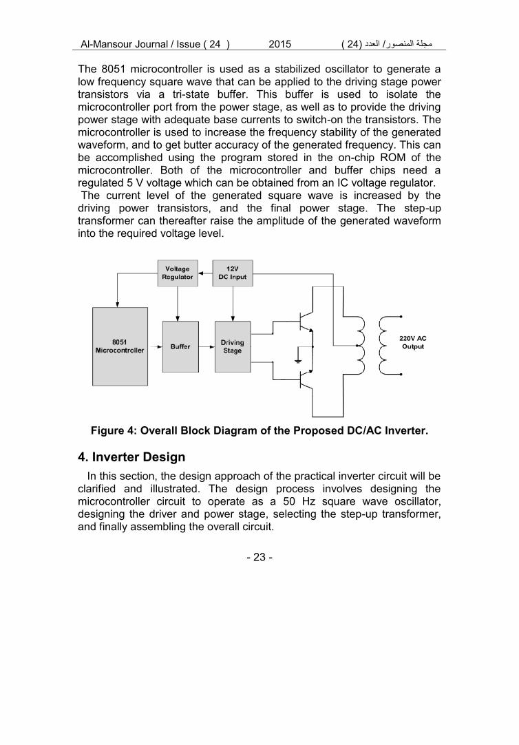
3. The Proposed Inverter CircuitFigure 4 presents a generalized diagram for the proposed inverter. To
simplify the analysis of the circuit, one can divide it into several stages anddeal with each stage independently.This circuit uses BJT transistors as switching devices and a center-tapstep-up transformer to convert a 12 V DC input into a 220 V AC output.The output waveform of this circuit is a square wave, and the power outputdepends on the transformer power rating, in addition to the current ratingof the power transistors.
Al-Mansour Journal / Issue ( 24 ) 2015 ) 24(العدد /مجلة المنصور
- 23 -
The 8051 microcontroller is used as a stabilized oscillator to generate alow frequency square wave that can be applied to the driving stage powertransistors via a tri-state buffer. This buffer is used to isolate themicrocontroller port from the power stage, as well as to provide the drivingpower stage with adequate base currents to switch-on the transistors. Themicrocontroller is used to increase the frequency stability of the generatedwaveform, and to get butter accuracy of the generated frequency. This canbe accomplished using the program stored in the on-chip ROM of themicrocontroller. Both of the microcontroller and buffer chips need aregulated 5 V voltage which can be obtained from an IC voltage regulator.The current level of the generated square wave is increased by the
driving power transistors, and the final power stage. The step-uptransformer can thereafter raise the amplitude of the generated waveforminto the required voltage level.
Figure 4: Overall Block Diagram of the Proposed DC/AC Inverter.
4. Inverter DesignIn this section, the design approach of the practical inverter circuit will be
clarified and illustrated. The design process involves designing themicrocontroller circuit to operate as a 50 Hz square wave oscillator,designing the driver and power stage, selecting the step-up transformer,and finally assembling the overall circuit.

Hawraa Qasim Hameed Firas Mohammed Ali Al-Raieحوراء قاسم حمید. م.، مفراس محمد علي.م.م
- 24 -
4.1 Designing the 8051 Microcontroller-Based Oscillator CircuitThe purpose of the oscillator circuit is to provide a clean square wave withan ideal frequency of 50 Hz, which is the frequency of the required ACvoltage.In order to generate a stabilized low frequency signal, it is preferred toproduce first a high frequency signal from a crystal oscillator, and then usefrequency dividers to obtain the required low frequency. This techniquecan be realized in software by programming a microcontroller to generatethe required square waves with a pre-determined time delays.The Atmel 89C51 microcontroller chip has been selected for this design.
This is a special IC of the 8051 family. It is a low cost 8-bit microcontrollerwith an internal Flash ROM code memory of 4 KB, and an internal RAM of128 B. It possesses 4 I/O ports, each containing 8 lines and has also two16-bit internal timers and one serial port.The timers of the 8051 microcontroller are referred as Timer 0 and Timer
1. They can be used as either timers or counters. Each 16-bit timer isimplemented by two 8-bit registers as low byte and high byte. For timer 0,the low byte is referred as TL0, while the high byte is referred as TH0. ForTimer 1, the equivalent registers are TL1 and TH1 respectively. Each timercan operate in four different modes depending on the codeword saved in aspecialized register called TMOD. In mode 1, the operation is 16-bittimer/counter with the TH and TL registers are cascaded. Each timerneeds a clock pulse to start. The clock frequency for the timers of the 8051equals the crystal frequency divided by 12 [6]. For example, if the crystalfrequency is 10 MHz, then the clock frequency will be 833.333 kHz, andthe clock interval will thus equal to 1.2 µs.
The starting and stopping process of the timers can be controlled viasoftware by setting and clearing a special flag bit, called TR (timer start),respectively. Before starting the timer, registers TL and TH should beloaded with certain initial values. The 16-bit timer can be loaded withvalues ranging from 0000H up to FFFFH. After loading the timer, it startsto count up starting from the initial preset value. When the timer reachesits maximum allowable value (FFFFH), it overflows and resets to 0. Thiscondition can be monitored through a special flag bit, called TF (timerflag). When the timer overflows, TF becomes 1. When the timer flag israised, the timer can be stopped by clearing the TR bit. In order to repeatthe counting process, the registers TH and TL must be reloaded with theoriginal value, and the TF flag must be reset to 0.
Al-Mansour Journal / Issue ( 24 ) 2015 ) 24(العدد /مجلة المنصور
- 25 -
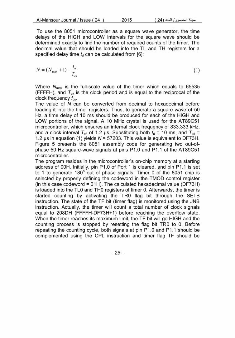
To use the 8051 microcontroller as a square wave generator, the timedelays of the HIGH and LOW intervals for the square wave should bedetermined exactly to find the number of required counts of the timer. Thedecimal value that should be loaded into the TL and TH registers for aspecified delay time td can be calculated from [6]:
ck
d
TtNN )1( max (1)
Where Nmax is the full-scale value of the timer which equals to 65535(FFFFH), and Tck is the clock period and is equal to the reciprocal of theclock frequency fck.The value of N can be converted from decimal to hexadecimal beforeloading it into the timer registers. Thus, to generate a square wave of 50Hz, a time delay of 10 ms should be produced for each of the HIGH andLOW portions of the signal. A 10 MHz crystal is used for the AT89C51microcontroller, which ensures an internal clock frequency of 833.333 kHz,and a clock interval Tck of 1.2 µs. Substituting both td = 10 ms, and Tck =1.2 µs in equation (1) yields N = 57203. This value is equivalent to DF73H.Figure 5 presents the 8051 assembly code for generating two out-of-phase 50 Hz square-wave signals at pins P1.0 and P1.1 of the AT89C51microcontroller.The program resides in the microcontroller’s on-chip memory at a startingaddress of 00H. Initially, pin P1.0 of Port 1 is cleared, and pin P1.1 is setto 1 to generate 180o out of phase signals. Timer 0 of the 8051 chip isselected by properly defining the codeword in the TMOD control register(in this case codeword = 01H). The calculated hexadecimal value (DF73H)is loaded into the TL0 and TH0 registers of timer 0. Afterwards, the timer isstarted counting by activating the TR0 flag bit through the SETBinstruction. The state of the TF bit (timer flag) is monitored using the JNBinstruction. Actually, the timer will count a total number of clock signalsequal to 208DH (FFFFH-DF73H+1) before reaching the overflow state.When the timer reaches its maximum limit, the TF bit will go HIGH and thecounting process is stopped by resetting the flag bit TR0 to 0. Beforerepeating the counting cycle, both signals at pin P1.0 and P1.1 should becomplemented using the CPL instruction and timer flag TF should be

Hawraa Qasim Hameed Firas Mohammed Ali Al-Raieحوراء قاسم حمید. م.، مفراس محمد علي.م.م
- 26 -
cleared. This process is repeated continuously to obtain two anti-phase50% duty cycle pulse signals.The assembly program has been converted to hex file using the MIDE-51
assembler, and then burned into the flash memory of the microcontrollerusing a commercial universal programmer.
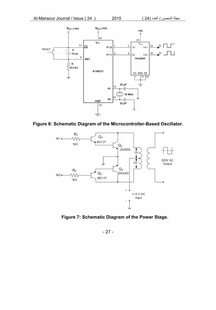
Figure 6 shows the schematic diagram of the AT89C51 microcontroller togenerate the 50 Hz square wave signals. The 74LS244 tri-state buffer isconnected to Port 1 of the microcontroller in order to isolate it from thepower stage, and to provide the power transistors with the necessarycurrent for driving them.
Figure 5: The Assembly Program Used to Generate the 50 Hz Signals.
4.2 Designing the Power StageThe second stage in the inverter design is to synthesize the transistor
power circuit in order to increase the current and voltage levels of thegenerated square waves. This circuit consists of two pairs of transistorsconnected in Darlington configuration in order to increase the current gain[7]. This circuit actually operates in the push/pull mode. Figure 7 shows aschematic diagram of the circuit.
Al-Mansour Journal / Issue ( 24 ) 2015 ) 24(العدد /مجلة المنصور
- 27 -
Figure 6: Schematic Diagram of the Microcontroller-Based Oscillator.
Figure 7: Schematic Diagram of the Power Stage.
Hawraa Qasim Hameed Firas Mohammed Ali Al-Raieحوراء قاسم حمید. م.، مفراس محمد علي.م.م
- 28 -
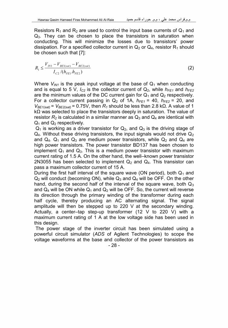
Resistors R1 and R2 are used to control the input base currents of Q1 andQ3. They can be chosen to place the transistors in saturation whenconducting. This will minimize the losses due to transistors’ powerdissipation. For a specified collector current in Q2 or Q4, resistor R1 shouldbe chosen such that [7]:
)./( 212
)(2)(111
FEFEC
satBEsatBEIN
hhIVVV
R
(2)
Where VIN1 is the peak input voltage at the base of Q1 when conductingand is equal to 5 V, IC2 is the collector current of Q2, while hFE1 and hFE2are the minimum values of the DC current gain for Q1 and Q2 respectively.For a collector current passing in Q2 of 1A, hFE1 = 40, hFE2 = 20, andVBE1(sat) = VBE2(sat) = 0.75V, then R1 should be less than 2.8 kΩ. A value of 1kΩ was selected to place the transistors deeply in saturation. The value ofresistor R2 is calculated in a similar manner as Q3 and Q4 are identical withQ1 and Q2 respectively.Q1 is working as a driver transistor for Q2, and Q3 is the driving stage of
Q4. Without these driving transistors, the input signals would not drive Q2and Q4. Q1 and Q3 are medium power transistors, while Q2 and Q4 arehigh power transistors. The power transistor BD137 has been chosen toimplement Q1 and Q3. This is a medium power transistor with maximumcurrent rating of 1.5 A. On the other hand, the well–known power transistor2N3055 has been selected to implement Q2 and Q4. This transistor canpass a maximum collector current of 15 A.During the first half interval of the square wave (ON period), both Q1 andQ2 will conduct (becoming ON), while Q3 and Q4 will be OFF. On the otherhand, during the second half of the interval of the square wave, both Q3and Q4 will be ON while Q1 and Q2 will be OFF. So, the current will reverseits direction through the primary winding of the transformer during eachhalf cycle, thereby producing an AC alternating signal. The signalamplitude will then be stepped up to 220 V at the secondary winding.Actually, a center–tap step-up transformer (12 V to 220 V) with amaximum current rating of 1 A at the low voltage side has been used inthis design.The power stage of the inverter circuit has been simulated using a
powerful circuit simulator (ADS of Agilent Technologies) to scope thevoltage waveforms at the base and collector of the power transistors as
Al-Mansour Journal / Issue ( 24 ) 2015 ) 24(العدد /مجلة المنصور
- 29 -
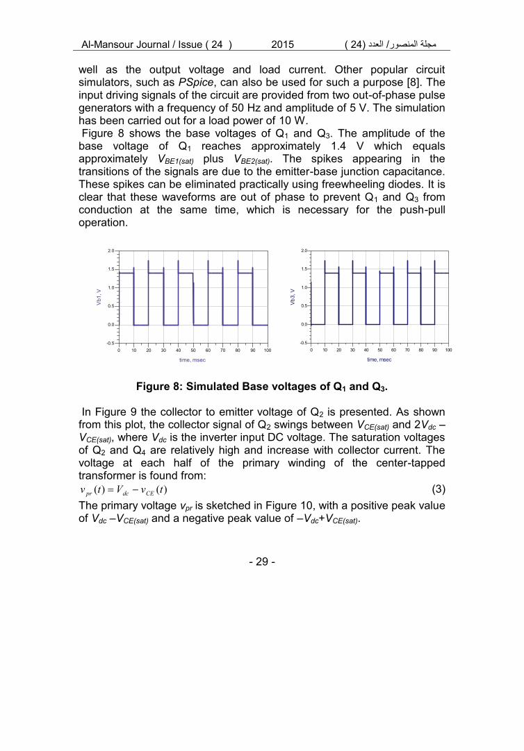
well as the output voltage and load current. Other popular circuitsimulators, such as PSpice, can also be used for such a purpose [8]. Theinput driving signals of the circuit are provided from two out-of-phase pulsegenerators with a frequency of 50 Hz and amplitude of 5 V. The simulationhas been carried out for a load power of 10 W.Figure 8 shows the base voltages of Q1 and Q3. The amplitude of the
base voltage of Q1 reaches approximately 1.4 V which equalsapproximately VBE1(sat) plus VBE2(sat). The spikes appearing in thetransitions of the signals are due to the emitter-base junction capacitance.These spikes can be eliminated practically using freewheeling diodes. It isclear that these waveforms are out of phase to prevent Q1 and Q3 fromconduction at the same time, which is necessary for the push-pulloperation.
Figure 8: Simulated Base voltages of Q1 and Q3.
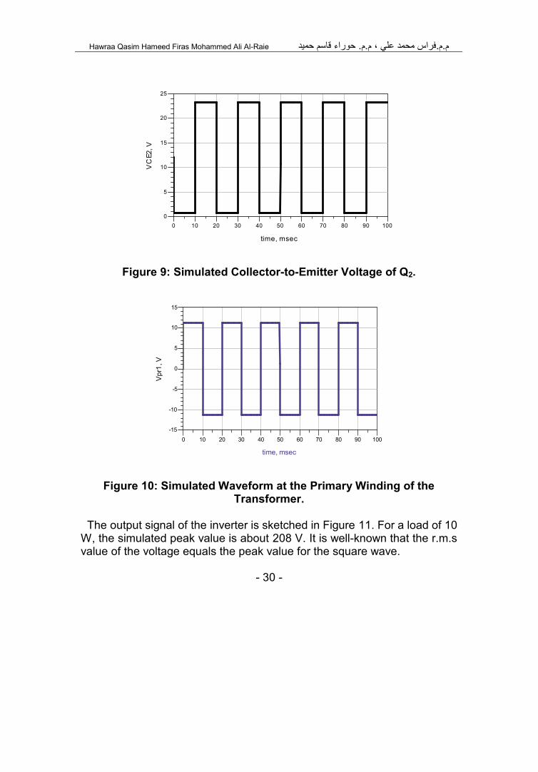
In Figure 9 the collector to emitter voltage of Q2 is presented. As shownfrom this plot, the collector signal of Q2 swings between VCE(sat) and 2Vdc –VCE(sat), where Vdc is the inverter input DC voltage. The saturation voltagesof Q2 and Q4 are relatively high and increase with collector current. Thevoltage at each half of the primary winding of the center-tappedtransformer is found from:
)()( tvVtv CEdcpr (3)The primary voltage vpr is sketched in Figure 10, with a positive peak valueof Vdc –VCE(sat) and a negative peak value of –Vdc+VCE(sat).
10 20 30 40 50 60 70 80 900 100
0.0
0.5
1.0
1.5
-0.5
2.0
time, msec
Vb1
,V
10 20 30 40 50 60 70 80 900 100
0.0
0.5
1.0
1.5
-0.5
2.0
time, msec
Vb3,
V
Hawraa Qasim Hameed Firas Mohammed Ali Al-Raieحوراء قاسم حمید. م.، مفراس محمد علي.م.م
- 30 -
Figure 9: Simulated Collector-to-Emitter Voltage of Q2.
Figure 10: Simulated Waveform at the Primary Winding of theTransformer.
The output signal of the inverter is sketched in Figure 11. For a load of 10W, the simulated peak value is about 208 V. It is well-known that the r.m.svalue of the voltage equals the peak value for the square wave.
10 20 30 40 50 60 70 80 900 100
5
10
15
20
0
25
time, msec
VC
E2,V
10 20 30 40 50 60 70 80 900 100
-10
-5
0
5
10
-15
15
time, msec
Vpr
1,V
Al-Mansour Journal / Issue ( 24 ) 2015 ) 24(العدد /مجلة المنصور
- 31 -
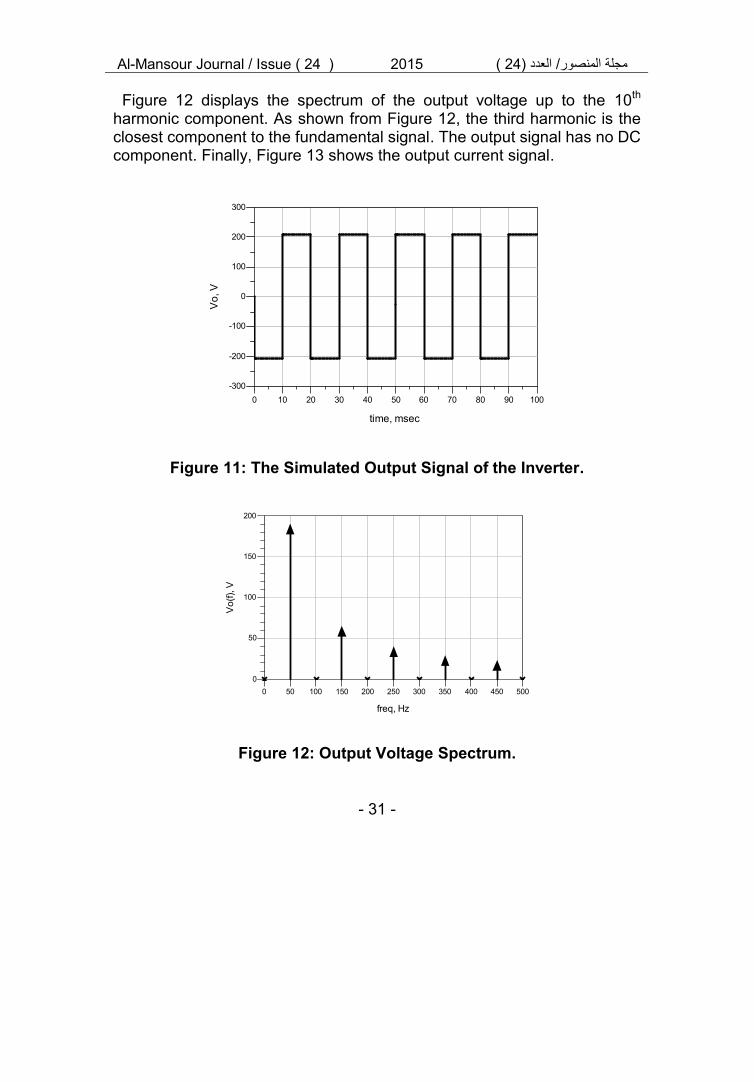
Figure 12 displays the spectrum of the output voltage up to the 10th
harmonic component. As shown from Figure 12, the third harmonic is theclosest component to the fundamental signal. The output signal has no DCcomponent. Finally, Figure 13 shows the output current signal.
Figure 11: The Simulated Output Signal of the Inverter.
Figure 12: Output Voltage Spectrum.
10 20 30 40 50 60 70 80 900 100
-200
-100
0
100
200
-300
300
time, msec
Vo,
V
50 100 150 200 250 300 350 400 4500 500
50
100
150
0
200
freq, Hz
Vo(
f), V

Hawraa Qasim Hameed Firas Mohammed Ali Al-Raieحوراء قاسم حمید. م.، مفراس محمد علي.م.م
- 32 -
Figure 13: Simulated Load Current.
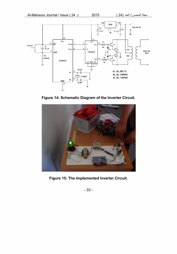
5. Circuit Construction and TestingFigure 14 shows the schematic diagram of the final inverter circuit. The
5V DC input voltage of the AT89C51 microcontroller and the 74LS244buffer is obtained from a 7805 IC regulator that has been connected to the12V DC input as shown in Figure 14.This regulator can be used to providea constant 5V DC voltage for the TTL or CMOS digital ICs for stableoperation. Two fast switching diodes, D1 and D2, are connected at thebases of Q1 and Q3 to remove the negative spikes of the base signalswhich may otherwise damage the emitter-base junctions of the transistors.The inverter circuit was implemented on a test breadboard, and all the
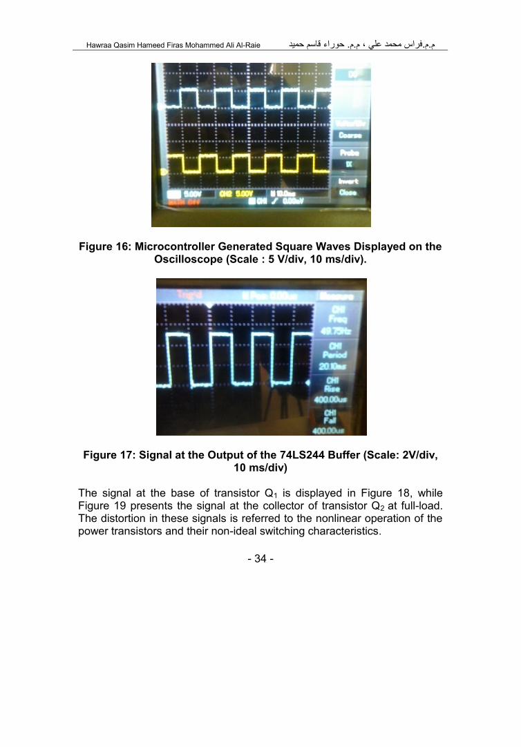
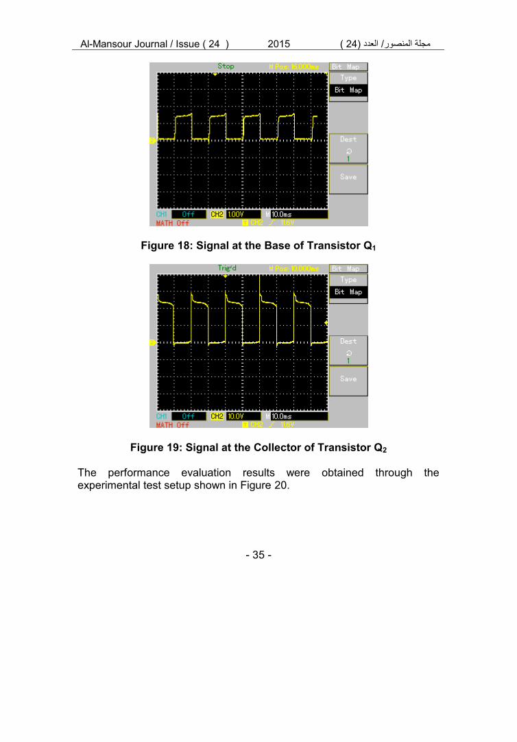
power transistors were fixed on suitable heat sinks. Figure 15 depicts aphotograph of the assembled circuit. As illustrated in Figure 15, the DCinput voltage is taken from a 12V DC battery of high capacity. In Figure 16,the square waves generated by the 8051 microcontroller at pins P1.0 andP1.1 are displayed on a digital storage oscilloscope. As shown from thisfigure, the generated signals are clean with constant amplitude of 5 V. Themeasured stabilized frequency is 49.75 Hz as depicted in Figure17.
10 20 30 40 50 60 70 80 900 100
-40
-20
0
20
40
-60
60
time, msec
io, m
A
Al-Mansour Journal / Issue ( 24 ) 2015 ) 24(العدد /مجلة المنصور
- 33 -
Figure 14: Schematic Diagram of the Inverter Circuit.
Figure 15: The Implemented Inverter Circuit.
Hawraa Qasim Hameed Firas Mohammed Ali Al-Raieحوراء قاسم حمید. م.، مفراس محمد علي.م.م
- 34 -
Figure 16: Microcontroller Generated Square Waves Displayed on theOscilloscope (Scale : 5 V/div, 10 ms/div).
Figure 17: Signal at the Output of the 74LS244 Buffer (Scale: 2V/div,10 ms/div)
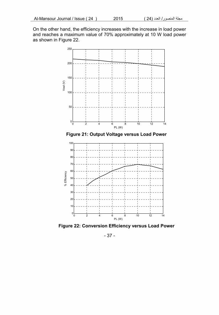
The signal at the base of transistor Q1 is displayed in Figure 18, whileFigure 19 presents the signal at the collector of transistor Q2 at full-load.The distortion in these signals is referred to the nonlinear operation of thepower transistors and their non-ideal switching characteristics.
Al-Mansour Journal / Issue ( 24 ) 2015 ) 24(العدد /مجلة المنصور
- 35 -
Figure 18: Signal at the Base of Transistor Q1
Figure 19: Signal at the Collector of Transistor Q2
The performance evaluation results were obtained through theexperimental test setup shown in Figure 20.

Hawraa Qasim Hameed Firas Mohammed Ali Al-Raieحوراء قاسم حمید. م.، مفراس محمد علي.م.م
- 36 -
Figure 20: Practical Test Setup for the Designed Inverter.
In this test setup, a 12 V car battery was used for DC input and 220 V, 2 Wbulbs (lamps) were used for the AC load. The input voltage, input current,output current, and output voltage have been measured while changingthe wattage of the load bulbs. The output voltage actually falls with aheavy load. The consumption of power by the bulbs changes with thevoltage.Figure 21 shows a sketch of the output voltage versus load power, while
Figure 22 shows a sketch of the inverter efficiency versus load powerwhere:
100..100 dcdc
outout
in
out
IVIV
PP (4)
Where Vdc and Idc are the DC input voltage and current respectively, andVout and Iout are the r.m.s voltage and current at the output.
It can be seen from Figure 21 that the output voltage falls with increasingload power and reaches to 200 V approximately at 10 W output (Full-load).From this figure, the AC voltage regulation can be calculated as:
100
FL
FLNL
VVVVR (5)
%8200200216
Where VNL is the no-load output voltage and VFL is the full-load outputvoltage.
Al-Mansour Journal / Issue ( 24 ) 2015 ) 24(العدد /مجلة المنصور
- 37 -
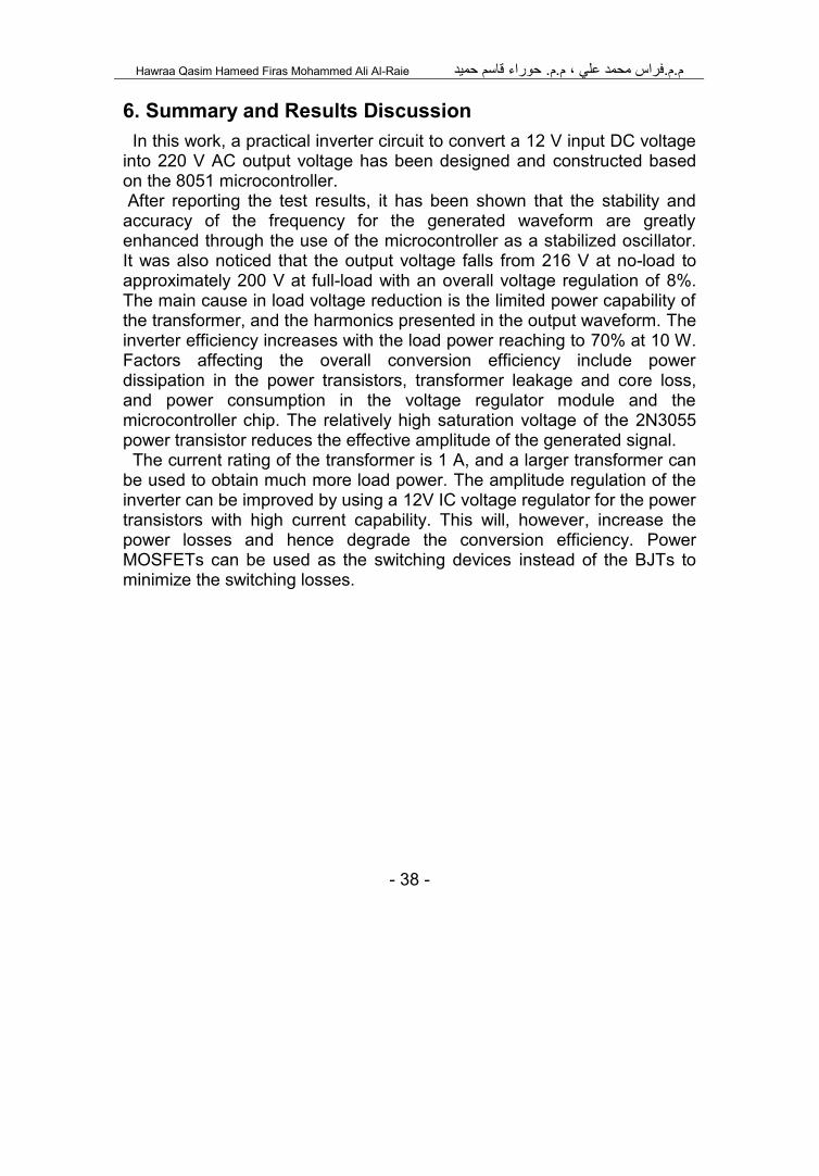
On the other hand, the efficiency increases with the increase in load powerand reaches a maximum value of 70% approximately at 10 W load poweras shown in Figure 22.
Figure 21: Output Voltage versus Load Power
Figure 22: Conversion Efficiency versus Load Power
0 2 4 6 8 10 12 140
50
100
150
200
250
PL (W)
Vou
t (V
)
0 2 4 6 8 10 12 140
10
20
30
40
50
60
70
80
90
100
PL (W)
% E
ffici
ency
Hawraa Qasim Hameed Firas Mohammed Ali Al-Raieحوراء قاسم حمید. م.، مفراس محمد علي.م.م
- 38 -
6. Summary and Results DiscussionIn this work, a practical inverter circuit to convert a 12 V input DC voltage
into 220 V AC output voltage has been designed and constructed basedon the 8051 microcontroller.After reporting the test results, it has been shown that the stability and
accuracy of the frequency for the generated waveform are greatlyenhanced through the use of the microcontroller as a stabilized oscillator.It was also noticed that the output voltage falls from 216 V at no-load toapproximately 200 V at full-load with an overall voltage regulation of 8%.The main cause in load voltage reduction is the limited power capability ofthe transformer, and the harmonics presented in the output waveform. Theinverter efficiency increases with the load power reaching to 70% at 10 W.Factors affecting the overall conversion efficiency include powerdissipation in the power transistors, transformer leakage and core loss,and power consumption in the voltage regulator module and themicrocontroller chip. The relatively high saturation voltage of the 2N3055power transistor reduces the effective amplitude of the generated signal.
The current rating of the transformer is 1 A, and a larger transformer canbe used to obtain much more load power. The amplitude regulation of theinverter can be improved by using a 12V IC voltage regulator for the powertransistors with high current capability. This will, however, increase thepower losses and hence degrade the conversion efficiency. PowerMOSFETs can be used as the switching devices instead of the BJTs tominimize the switching losses.
Al-Mansour Journal / Issue ( 24 ) 2015 ) 24(العدد /مجلة المنصور
- 39 -
References[1] Fang L. Luo and Hong Ye, “Advanced DC/AC Inverters: Applications
in Renewable Energy”, Taylor & Francis Group, LLC, 2013.[2] Denis Fewson, “Introduction to Power Electronics”, Oxford University
Press, New York, USA, 1998.[3] James H. Hahn, “Modified Sine Wave Inverter Enhanced”, Power
Electronics Technology, August 2006, pp. 20-22.[4] M. U. Rafique, S. Aslan, and J. Anwer, “Implementation of a Novel
Microcontroller-Based Voltage Source Sine-Wave Inverter”,Proceedings of the 2011 Frontiers of Information Technology, pp.167-172.
[5] A. S. K. Chowdhury et al., “Design and Implementation of a HighlyEfficient Pure Sine-Wave Inverter for Photovoltaic Applications”,Proceedings of the 2013 International Conference on Informatics,Electronics & Vision (ICIEV), 17-18 May 2013, pp. 1-6.
[6] Muhammad Ali Mazidi, Janice G. Mazidi, and Rolin D. McKinlay,“The 8051 Microcontroller and Embedded Systems Using Assemblyand C”, 2nd Edition, Prentice-Hall, New-Delhi, India, 2006.
[7] Bob Cordell, “Designing Audio Power Amplifiers”, McGraw-HillCompanies, Inc., 2011.
[8] M. H. Rashid, and H. M. Rashid, “SPICE for Power Electronics andElectric Power”, 2nd Edition, Tylor & Francis Group, LLC, 2006.

Hawraa Qasim Hameed Firas Mohammed Ali Al-Raieحوراء قاسم حمید. م.، مفراس محمد علي.م.م
- 40 -
باستخدام المسیطر الدقیقناوبتیار مت/ تصمیم وتنفیذ عاكس تیار مستمر
*حوراء قاسم حمید. م.م*فراس محمد علي الراعي. م.م
المستخلص
لدوائر ستقراریة الترددیة ودقة تردد اإلشارة المتولدة لتحسین اإلفي ھذا البحث تم اقتراح طریقةالمسیطر باستخدامعن طریق استخدام دائرة مذبذب عالي االستقرار مبنیة العاكس ذات اإلشارة المربعة
.الدقیقلیعمل كمذبذب عالي االستقرار لتولید 8051على استخدام المسیطر الدقیق المقترحةتقنیة التعتمد
عن لدائرة العاكس إلى مرحلة مشغل القدرة وإرسالھما Hz 50إشارتین مربعتین متعاكستین بالطور بتردد یتم بعد ذلك تضخیم ھذه اإلشارات لزیادة مستوى التیار . طریق برنامج مخزون في ذاكرتھ الداخلیة الدائمیة
السحب بترانزستورات قدرة من نوع /والفولتیة فیھا عن طریق مضخم قدرة تحویلي یعمل بطریقة الدفعBJT .واسطة محول رافع للجھدالمتولدة الى القیمة المطلوبة بناوبةویتم رفع جھد اإلشارة المت.
قیمتھ الفعالة ناوبإلى جھد متV 12تم تصمیم وتنفیذ دائرة عاكس عملیة لتحویل جھد مستمر مقداره 220 V وعازل 8051تتكون الدائرة المقترحة من المسیطر الدقیق . 8051باستخدام المسیطر الدقیق
محاكاة دائرة تتم.محول رافع للجھدومضخم قدرة أولي ومرحلة تضخیم قدرة نھائیة باإلضافة إلىوقد بینت نتائج القیاسات العملیة بأن الدائرة . العاكس بواسطة الحاسوب ومن ثم تنفیذھا واختبارھا عملیا
10تعطي قدرة خرج مقدارھا W وبكفاءة تحویل قصوى تصل إلى %8للحمل الكامل بتنظیم جھد مقداره70%.
الجامعة التكنولوجیةقسم الھندسة الكھربائیة،*