design of an 8 bit differential paired efu se otp … · design of an 8 bit differential paired efu...
TRANSCRIPT

J. Cent. South Univ. (2012) 19: 168−173 DOI: 10.1007/s11771−012−0987−4
Design of an 8 bit differential paired eFuse OTP memory IP reducing sensing resistance
JANG JiHye, JIN Liyan(金丽妍), JEON HwangGon, KIM KwangIl, HA PanBong, KIMYoungHee
Department of Electronic Engineering, Changwon National University, 9 SarimDong, Changwon 641773, Korea
© Central South University Press and SpringerVerlag Berlin Heidelberg 2012
Abstract: For the conventional singleended eFuse cell, sensing failures can occur due to a variation of a postprogram eFuse resistance during the data retention time and a relatively high program resistance of several kilo ohms. A differential paired eFuse cell is designed which is about half the size smaller in sensing resistance of a programmed eFuse link than the conventional singleended eFuse cell. Also, a sensing circuit of sense amplifier is proposed, based on D flipflop structure to implement a simple sensing circuit. Furthermore, a sensing margin test circuit is proposed with variable pullup loads out of consideration for resistance variation of a programmed eFuse. When an 8 bit eFuse OTP IP is designed with 0.18 µm standard CMOS logic of TSMC, the layout dimensions are 229.04 µm × 100.15 µm. All the chips function successfully when 20 test chips are tested with a program voltage of 4.2 V.
Key words: eFuse; differential paired efuse cell; one time programmable memory; sensing resistance; D flipflop based sense amplifier
1 Introduction
In general, program memories used for PMICs (Power management ICs), LCD display ICs, and CMOS image sensors are OTP (Onetime programmable) memories since they can be designed based on a logic process of eFuse or antifuse type which does not require any additional processes [1−2]. The OTP memory of antifuse type is programmed by shortening electrically from the breakdown mechanism when a high voltage is applied to a MOS transistor with a thin gate oxide [3−4]. The OTP cell of antifuse type requires a comparatively elaborate sensing circuit [5−6] since its postprogram resistance becomes several mega ohms. In contrast, the OTP memory of eFuse type is programmed by flowing an overcurrent through the eFuse [7−8]. The pre program resistance of the eFuse cell is 50−100 Ω and the postprogram resistance is more than several kilo ohms. Thus, the eFuse is programmed into either a conductive state or highly resistive state [9−10]. Generally, the eFusetype OTP memory is applied to performing analog trimming as a smalldensity memory [11−12].
An eFuse OTP cell is classified into a singleport eFuse cell [13−14] and a dualport eFuse cell [15]. The singleport eFuse cell shares its read and write ports, has the program resistance of several kilo ohms, and adopts an analog sensing scheme. In contrast, the dualport eFuse cell has separated read and write ports and has the program resistance of several ten kilo ohms since it uses
a NMOS transistor with large channel width to flow a large programming current. The peripheral circuit is simple since a digital sensing scheme can be adopted. A dualport eFuse cell consists of an eFuse link, a program NMOS transistor with large channel width that can flow a large programming current, and a read NMOS transistor with small channel width that can reduce a read current in the read mode [2].
For the eFuse cell, sensing failures occur since the resistance of a programmed eFuse link can vary during the data retention time and hence the postprogram eFuse resistance decreases. Also, sensing failures can occur and yield can drop for some eFuse OTP memory of which the program resistance is about several kilo ohms.
In this work, a proposed differential paired eFuse cell is described, which can reduce sensing resistance of a programmed eFuse link. In addition, a simpler sensing circuit of D flipflop structure is described. Finally, a sensing margin test circuit with a variable pullup load is also described out of consideration for resistance variations of programmed eFuse. An 8 bit eFuse OTP memory IP is designed with 0.18 µm generic CMOS process of TSMC.
2 Circuit design
The trends in the development of an eFuse OTP cell are summarized in Table 1. The capacities of recently published OTP memory IPs are in the range of
Received date: 2011−04−26; Accepted date: 2011−10−10 Corresponding author: KIM YoungHee, Professor, PhD; Tel: +82−55−285−1023; Email: [email protected]
J. Cent. South Univ. (2012) 19: 168−173 169
Table 1 Trends in development of eFuse OTP cell
Ref. Process/ nm Cell circuit Cell size/ μm 2
Memory density/ bit
Sensing scheme
[13] 32 1.37 4 096 Analog
[14] 45 3.6 4 096 Analog
[15] 90 74.23 512 Digital
512−4 kbit [13−15]. For the conventional singleended eFuse cell, sensing failures can occur due to a variation of a postprogram eFuse resistance during the data retention time and a relatively high program resistance of several kilo ohms.
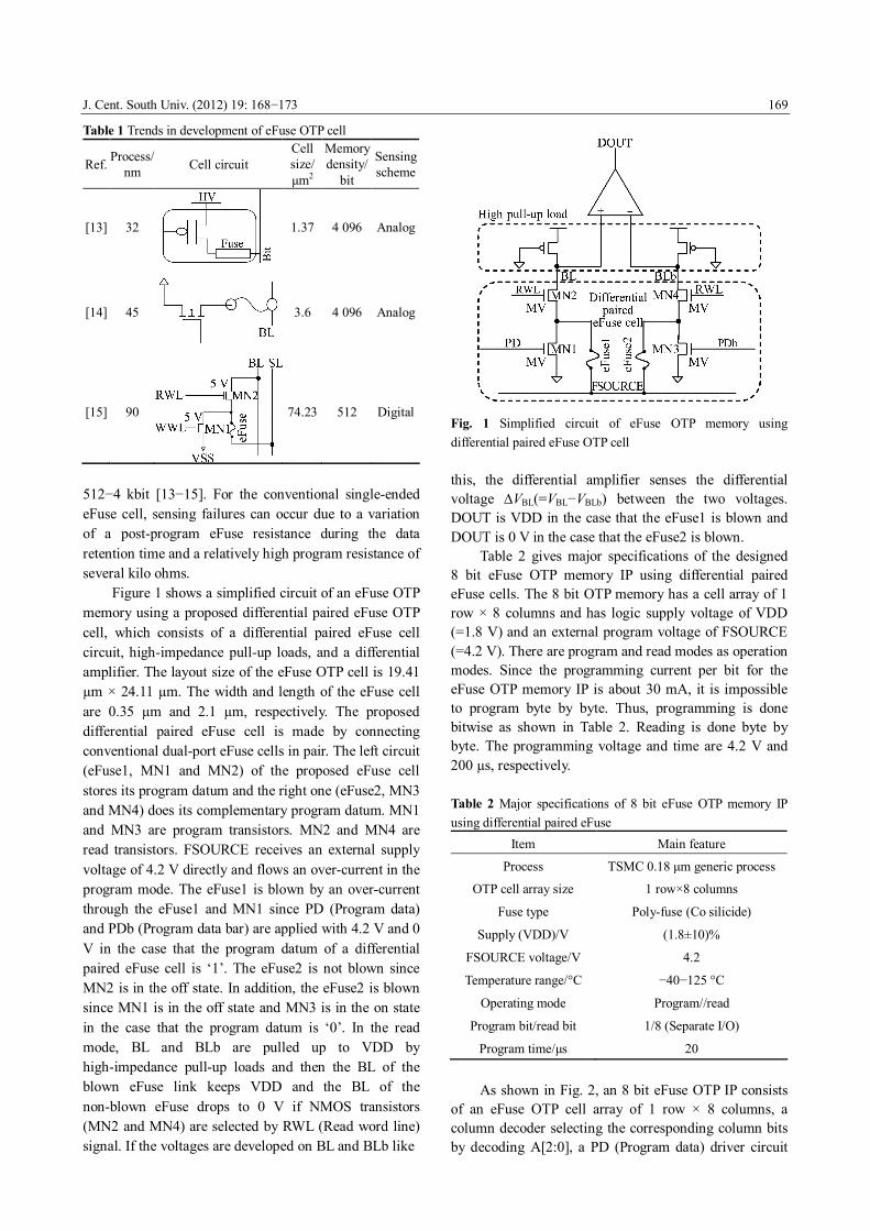
Figure 1 shows a simplified circuit of an eFuse OTP memory using a proposed differential paired eFuse OTP cell, which consists of a differential paired eFuse cell circuit, highimpedance pullup loads, and a differential amplifier. The layout size of the eFuse OTP cell is 19.41 µm × 24.11 µm. The width and length of the eFuse cell are 0.35 µm and 2.1 µm, respectively. The proposed differential paired eFuse cell is made by connecting conventional dualport eFuse cells in pair. The left circuit (eFuse1, MN1 and MN2) of the proposed eFuse cell stores its program datum and the right one (eFuse2, MN3 and MN4) does its complementary program datum. MN1 and MN3 are program transistors. MN2 and MN4 are read transistors. FSOURCE receives an external supply voltage of 4.2 V directly and flows an overcurrent in the program mode. The eFuse1 is blown by an overcurrent through the eFuse1 and MN1 since PD (Program data) and PDb (Program data bar) are applied with 4.2 V and 0 V in the case that the program datum of a differential paired eFuse cell is ‘1’. The eFuse2 is not blown since MN2 is in the off state. In addition, the eFuse2 is blown since MN1 is in the off state and MN3 is in the on state in the case that the program datum is ‘0’. In the read mode, BL and BLb are pulled up to VDD by highimpedance pullup loads and then the BL of the blown eFuse link keeps VDD and the BL of the nonblown eFuse drops to 0 V if NMOS transistors (MN2 and MN4) are selected by RWL (Read word line) signal. If the voltages are developed on BL and BLb like
Fig. 1 Simplified circuit of eFuse OTP memory using differential paired eFuse OTP cell
this, the differential amplifier senses the differential voltage ∆VBL(=VBL−VBLb) between the two voltages. DOUT is VDD in the case that the eFuse1 is blown and DOUT is 0 V in the case that the eFuse2 is blown.
Table 2 gives major specifications of the designed 8 bit eFuse OTP memory IP using differential paired eFuse cells. The 8 bit OTP memory has a cell array of 1 row × 8 columns and has logic supply voltage of VDD (=1.8 V) and an external program voltage of FSOURCE (=4.2 V). There are program and read modes as operation modes. Since the programming current per bit for the eFuse OTP memory IP is about 30 mA, it is impossible to program byte by byte. Thus, programming is done bitwise as shown in Table 2. Reading is done byte by byte. The programming voltage and time are 4.2 V and 200 µs, respectively.
Table 2 Major specifications of 8 bit eFuse OTP memory IP using differential paired eFuse
Item Main feature
Process TSMC 0.18 μm generic process
OTP cell array size 1 row×8 columns
Fuse type Polyfuse (Co silicide)
Supply (VDD)/V (1.8±10)%
FSOURCE voltage/V 4.2
Temperature range/°C −40−125 °C
Operating mode Program//read
Program bit/read bit 1/8 (Separate I/O)
Program time/μs 20
As shown in Fig. 2, an 8 bit eFuse OTP IP consists of an eFuse OTP cell array of 1 row × 8 columns, a column decoder selecting the corresponding column bits by decoding A[2:0], a PD (Program data) driver circuit

J. Cent. South Univ. (2012) 19: 168−173 170
driving the selected program data to the OTP cells, a BL S/A (Bitline sense amplifier) sensing and outputting the BL datum to the DOUT port, and a control logic that supplies internal control signals which are suitable for both the program and read modes with the control signals (RD, PGM, TM_EN). The BL S/A senses and outputs a datum coming out from BL[7:0] according to the programmed states to DOUT[7:0] digitally in the read mode. The functional test read mode and the normal read mode are classified by TM_EN (Test mode enable) signal.
Fig. 2 Block diagram of 8 bit eFuse OTP IP
Figure 3 shows a cell array circuit of 1 row × 8 columns using differential paired eFuse cells. There is RWL signal in the row direction, and there are BL[7:0], BLb[7:0], PD[7:0] and PDb[7:0] signals in the column direction. Also, there are FSOURCE and VSS as powers.
Fig. 3 Cell array of 1 row × 8 columns
Table 3 gives bias voltage conditions for various operation modes of each OTP cell node. Since RWL keeps at 0 V in the program mode, a read NMOS transistor turns off. PD and PDb of the nonselected cell by A[2:0] keep at 0 V. On the other hand, PD and PDb of the selected cell drive 0 V and 4.2 V in the case that DIN is ‘0’, and 4.2 V and 0 V in the case that DIN is ‘1’. In the program mode, the eFuse connected to BLb of the selected cell is blown in the case that DIN is ‘0’ and the eFuse connected to BL is blown in the case that DIN is ‘1’. FSOURCE voltage is forced to be 4.2 V in the program mode. On the other hand, the program transistor turns off since PD and PDb keep at 0 V. FSOURCE stays in the floating state but is biased to 0 V circuitally. BL and BLb are pulled up to VDD by the highimpedance pullup loads, and BL and BLb of the programmed cell with ‘0’ are 0 V and VDD and those of the programmed cell with ‘1’ are VDD and 0 V by RWL signal.
Figure 4 shows a layout image of a differential paired eFuse OTP memory cell. The layout dimensions of the OTP cell are 19.41 µm × 24.11 µm. The width and length of an eFuse link are 0.35 µm and 2.1 µm, respectively, as shown in Fig. 4.
Since COL_SEL is 0 V for nonselected cells by decoding A[2:0] in the program mode, the output signals of a PD driver, PD and PDb, keep at 0 V. On the other hand, PD and PDb drive 0 V and VPP in the case that DIN is ‘0’, and VPP and 0 V in the case that DIN is ‘1’ since COL_SEL is VDD for selected cells. An internal program voltage, VPP, is 4.2 V in the program mode. PD[7:0] and PDb[7:0] signals drive 0 V independently of DIN and COL_SEL signals since IPGMb (Internal program bar) keeps VDD in the read mode. VDD_PD signal protects the VDDtoVPP level translator circuit in Fig. 5 from flowing a shortcircuit current from the level translator before VDD is generated from the voltage regulator [2]. VPP switches to a higher supply between VDD and FSOURCE.
Figure 6 shows is a BL pullup load circuit which precharges BL and BLb to VSS by PRECHARGE signal
Table 3 Bias voltage conditions for various operation modes of each OTP cell node
Program mode Signal
Unselected cell Selected cell Read mode
DIN 0 1 0 1 0 1
RWL 0 0 0 0 VDD VDD
PD/V 0 0 0 4.2 0 0
PDb/V 0 0 4.2 0 0 0
FSOURCE/V 4.2 4.2 4.2 4.2 Floating Floating
BL Floating Floating Floating Floating 0 VDD
BLb Floating Floating Floating Floating VDD 0

J. Cent. South Univ. (2012) 19: 168−173 171
Fig. 4 Layout image of designed OTP cell
Fig. 5 PD driver circuit
Fig. 6 BL pullup load circuit
in the normal read mode. When RWL signal of an OTP cell is activated to VDD, BL and BLb are pulled up to VDD by pullup load transistors with large channel width (MP1 and MP2) while BL_LOADb signal is 0 V. At this moment, pullup transistors with small channel width (MP3 and MP4) for the test read mode are in the off state. All the pullup load transistors in Fig. 6 are designed to stay in the highimpedance state. Since the impedances of the pullup transistors are large, the bit line connected to a programmed eFuse is pulled up to VDD while the bit line connected to a nonprogrammed
eFuse keeps at VSS. In the case of reading a non programmed eFuse cell, a BL precharging voltage, VDD, discharges to 0 V through the read NMOS transistor and the eFuse link. At this moment, the eFuse can be blown by the EM (Electromigration) phenomenon since a highdensity current flows the eFuse link with narrow width. But we use a scheme of precharging a BL pair to VSS to reduce a read current through a nonprogrammed cell in this work. Thus, we can reduce a read current through a nonprogrammed eFuse.
In general, sensing failures can occur when the resistance of an eFuse link decreases during the data retention time for an eFuse OTP memory cell. Thus, a sensing margin test circuit is proposed with a variable pullup load out of consideration for resistance variation of a programmed eFuse. The variable pullup load can vary the impedance of the pullup load in the BL charging circuit used in the functional test read and normal read modes. Among pullup transistors in Fig. 6, MP3 and MP4 are used only for a functional test of the chip, and MP1 and MP2 are in the off state. In the test read mode, the differential input voltage of the differential amplifier decreases and a sensible eFuse resistance is larger than that in the normal read mode. Thus, the difference of the sensible eFuse resistances between in the functional test read mode and in the normal read mode is a marginal resistance during the data retention time.
Figure 7 shows a BL S/A circuit based on D flipflop which senses and latches the differential input voltage. The BL S/A is a negative edgetriggered D flipflop. While SAENb is high, N1 and N2 nodes keep high, and the SR latch circuit latches the previousstate datum. When SAENb is activated from high to low, BL and BLb are sensed and then the read data are transferred to the DOUT port.
Fig. 7 BL S/A circuit based on D flipflop circuit
Figure 8 shows a layout image of an 8 bit eFuse OTP IP. The layout dimensions of designed 8 bit eFuse OTP IP with 0.18 µm generic process of TSMC are 229.04 µm×100.15 µm (= 0.022 9 mm 2 ).
J. Cent. South Univ. (2012) 19: 168−173 172
Fig. 8 Layout image of 8 bit eFuse OTP IP
3 Simulation and measurement results
Figure 9 shows a simulation result of BL sensing voltage with respect to postprogram eFuse resistance according to the two read modes. Sensing resistances are 5.05 kΩ in the test mode and 1.58 kΩ in the normal mode when the sensing voltage of the BL S/A circuit is about 100 mV. Thus, we secure a margin of the resistance variation of programmed eFuse during the data retention time. Also, program yield increases since the eFuse sensing resistance of the differential paired eFuse OTP memory is several kilo ohms compared with several ten kilo ohms of the dualport eFuse OTP memory. Furthermore, the circuit of the differential paired eFuse OTP memory is simplified since the BL S/A circuit does not require the reference voltage generator compared with the singleport eFuse OTP memory.
Fig. 9 Simulation results of BL sensed voltages with respect to postprogram eFuse resistances according to read modes
Figure 10 shows simulation results in the normal read mode and in the program mode. At first, BL and BLb are precharged by PRECHARGE signal in the normal read mode. If RWL signal is activated to VDD, the read transistor of the eFuse OTP cell turns on. Then, the read data are transferred to BL and BLb while BL_LOADb signal is 0 V. If small signal voltages are developed on BL and BLb sufficiently, SAENb is
activated to be low, and the read data of BL and BLb are latched into the D flipflop and output to the DOUT port. The access time is 139 ns in the read mode. As shown in Fig. 10(b) in the program mode, nonselected PD and PDb are all 0 V, and selected PD and PDb are 4.2 V and 0 V when DIN is ‘1’.
Fig. 10 Simulation results: (a) In normal read mode; (b) In program mode
Figure 11 shows a DOUT waveform of an eFuse OTP IP according to function modes of a test chip. The DOUT functions normally for both a programmed cell with ‘0’ and a programmed cell with ‘1’. Also, all the chips function successfully when 20 test chips are tested with a program voltage of 4.2 V.

J. Cent. South Univ. (2012) 19: 168−173 173
Fig. 11Measured DOUT waveform of eFuse OTP IP according to function modes
4 Conclusions
1) A differential paired eFuse cell is proposed with about half the size smaller in sensing resistance of a programmed eFuse link than the conventional single ended eFuse cell.
2) A sensing circuit of sense amplifier based on D flipflop structure is proposed to implement a simple sensing circuit.
3) A sensing margin test circuit is proposed with variable pullup loads out of consideration for resistance variations of programmed eFuse. Sensing can be done normally although the sensed resistance of a programmed eFuse in the normal mode is lower by about 3.5 kΩ than that in the test mode since the sensed voltage in the normal mode is higher than that in the test mode for the programmed eFuse.
4) An 8 bit eFuse OTP memory IP is designed with 0.18 µm standard CMOS process of TSMC. All the chips function successfully when 20 test chips are tested with a program voltage of 4.2 V.
Acknowledgement This work is sponsored by ETRI System
Semiconductor Industry Promotion Center, Human Resource Development Project for SoC Convergence, Korea.
References
[1] CHA H K, YUN I H, KIM B J, SO B C, CHUN K H, NAM I K, LEE K. A 32KB standard CMOS antifuse onetime programmable rom embedded in a 16bit microcontroller [J]. IEEE Journal of SolidState Circuit, 2006, 41(9): 2115−2124.
[2] KULKARNI S H. Highdensity 3D metalfuse PROM featuring
1.37 µm 2 1T1R bit cell in 32nm highk metalgate CMOS technology [C]// Symposium on VLSI Circuits. USA: IEEE Press, 2009: 28−29.
[3] MATSUFUJI K, NAMEKAWA T, NAKANO H, ITO H, WADA O, OTSUKA N. A 65 nm pure CMOS onetime programmable memory using a twoport antifuse cell implemented in a matrix structure [C]// Proceedings of IEEE Asian SolidState Circuit Conference. Jeju: 2007: 212−215.
[4] LI Longzhen, KIM T H, SHIM O Y, PARK M H, HA P B, KIM Y H. Design of synchronous 256bit OTP memory [J]. KIMICS of Semiconductors and Communications, 2008, 12(7): 1227−1234.
[5] CHOI J S, WEE J K, CHO H Y, KIM P J, OH J K, LEE C H, CHUNG J Y, KIM S C, YANG W. Antifuse EPROM circuit for field programmable DRAM [C]// Proceedings of IEEE International SolidState Circuits Conference. San Francisco, 2000: 406−407.
[6] BARSATAN R, MAN T Y, CHAN M S. A zero mask onetime programmable memory array for RFID applications [C]// Proceedings of IEEE International Symposium on Circuits and Systems. Island of Kos, 2006: 975−978.
[7] ALAVI M, BOHR M, HICKS J, DENHAM M, CASSENS A, DOUGLAS D, TSAI M C. A PROM element based on silicide agglomeration of poly fuses in a CMOS logic process [C]// Proceedings of IEEE Electron Devices Meeting. Washington, 1997: 855−858.
[8] FELLNER J, BOESMUELLER P, REITER H. Lifetime study for a poly fuse in a 0.35 µm polycide CMOS process [C]// Proceedings of IEEE the 43rd Annual International Reliability Physics Symposium. San Jose, 2005: 446−449.
[9] FELLNER J, PREMSTAETTEN S. A one time programming cell using more than two resistance levels of a polyfuse [C]// Proceedings of IEEE Custom Integrated Circuits Conference. San Jose, 2005: 263−266.
[10] SAFRAN J, LESLIE A, FREDEMAN G, KOTHANDARAMAN C, CESTERO A, CHEN X, RAJEEVAKUMAR R, KIM D K, LI yanzun, MOY D, ROBSON N, KIRIHATA T, IYER S. A compact efuse programmable array memory for SOI CMOS [C]// Proceedings of Symposium on VLSI Circuits. Kyoto, 2007: 72−73.
[11] ELODIE E, BRUNO A, PHILIPPE C, PATRICE W. Review of fuse and antifuse solutions for advanced standard CMOS technologies [J]. Microelectronics Journal, 2009, 40(12): 1755−1765.
[12] KPTHANDARAMAN C, IYER S K, IYER S S. Electrically programmable fuse (efuse) using electromigration in silicides [J]. IEEE Electron Device Letters, 2002, 23(9): 523−525.
[13] ROBSON N, SAFRAN J, KOTHANDARAMAN, CESTERO A, CHEN X, RAJEEVAKUMAR, LESLIE A, MOY D, KINHATA T, IYER S. Electrically Programmable Fuse (eFuse): From memory redundancy to autonomic chips [C]// Proceedings of Custom Integrated Circuits Conference. San Jose: IEEE Press, 2007: 799−804.
[14] KIM D H, JANG J H, JIN L Y, LEE J H, HA P B, KIM Y H. Design and measurement of a 1kBit eFuse onetimeprogrammable memory IP based on a BCD process [J]. IEICE Trans Electron, 2010, E93C (8): 1365−1370.
[15] KIM J H, JANG J H, JIN L Y, HA P B, KIM Y H. Design of a lowpower OTP memory IP and its measurement [J]. Journal of the Korean Institute of Maritime Information and Communication Sciences, 2010, 14(11): 2541−2547.
(Edited by YANG Bing)