design of ingaas/inp 1.55 m vertical cavity surface ... · design of ingaas/inp 1.55μm vcsels i-...
TRANSCRIPT
Design of InGaAs/InP 1.55μm vertical cavity surface emitting lasers (VCSEL)
J.-M. Lamy, S. Boyer-Richard, C. Levallois, C. Paranthoën, H. Folliot, N. Chevalier, A. Le Corre, S. Loualiche
UMR FOTON 6082 CNRS, INSA de Rennes, France
8th International Conference on Numerical Simulation of Optoelectronic Devices, Nottingham, 4th September 2008
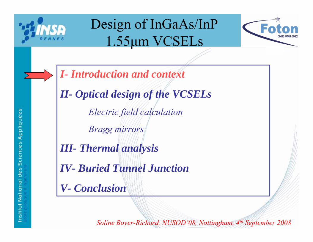
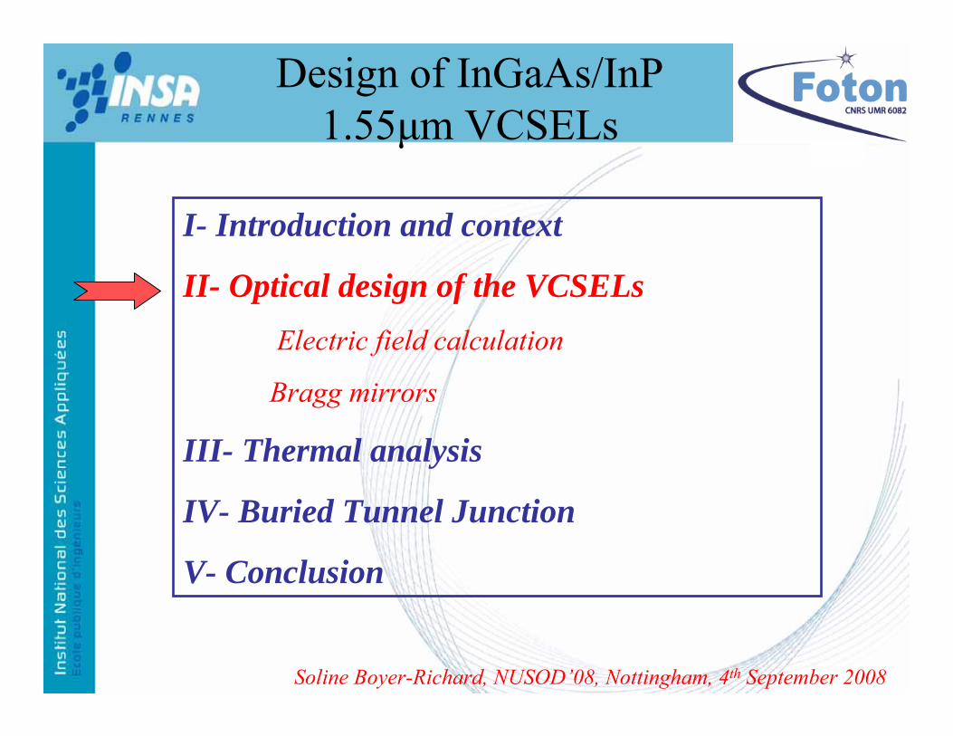
Design of InGaAs/InP1.55μm VCSELs
I- Introduction and context
II- Optical design of the VCSELsElectric field calculation
Bragg mirrors
III- Thermal analysis
IV- Buried Tunnel Junction
V- Conclusion
Soline Boyer-Richard, NUSOD’08, Nottingham, 4th September 2008
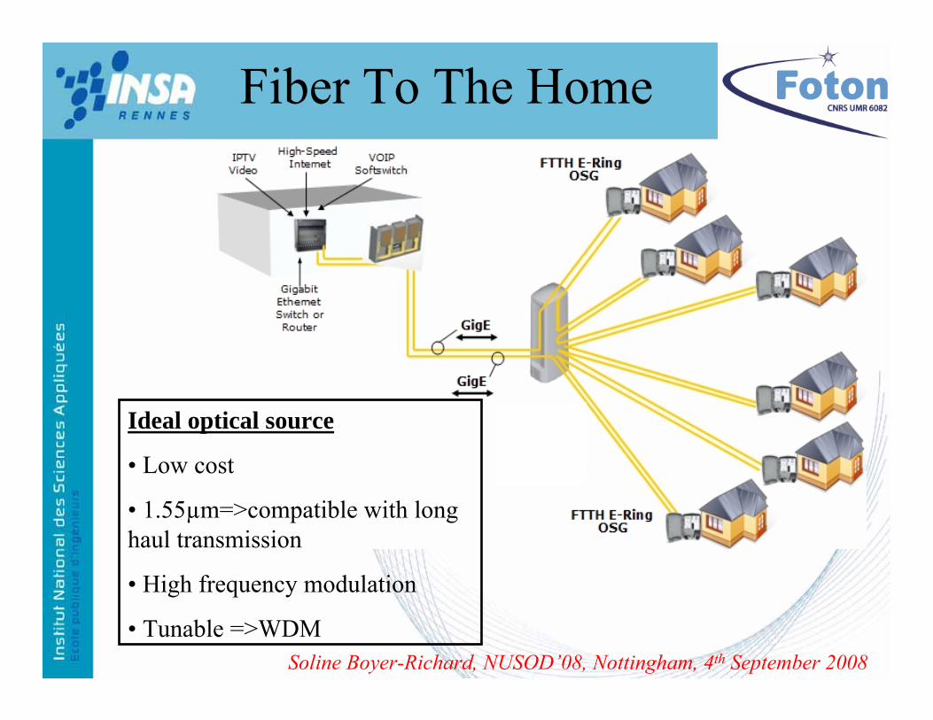
Fiber To The Home
Ideal optical source
• Low cost
• 1.55µm=>compatible with long haul transmission
• High frequency modulation
• Tunable =>WDMSoline Boyer-Richard, NUSOD’08, Nottingham, 4th September 2008

Surface Emitting Laser• Device tested before packaging• Array integration• Output circular mode shapeMicro-cavity• Small active region low Ith or Pth
• Short length Wide FSR
Advantages
VCSEL
Drawbacks Output powerThermal dependence
Substrate
Bottom mirror
Top mirror
active region 1~3 µm
Soline Boyer-Richard, NUSOD’08, Nottingham, 4th September 2008

Electrically pumped VCSEL
Soline Boyer-Richard, NUSOD’08, Nottingham, 4th September 2008
6QWs
InP n+
Q1.18 (30 nm)
Q1.18 (30 nm)
InP p+ Q1.18 p+ (10 nm) Q1.4 p++(25 nm) Q1.4 n++(25 nm) InP n+
Active zone
Bragg mirror
Bragg mirror
InP n+ Contact BTJ
CW 1.55 µm optically pumped VCSELs lattice-matched to InP with dielectric Bragg mirrors already demonstrated (J.M. Lamy et al., IPRM’08)
Electrically pumped VCSEL designed and fabricated at FOTON laboratory, within a collaborative ANR project named lambda-access
a-Si/a-SiNx DBR
active zone grown by MBE with 6 InGaAs QW on lattice-matched alloy In0.8Ga0.2As0.435P0.565 (Q1.18)
Buried Tunnel Junction in strongly doped lattice matched alloy Q1.4 (ND=NA=5.1019 cm-3)
Design of InGaAs/InP1.55μm VCSELs
I- Introduction and context
II- Optical design of the VCSELsElectric field calculation
Bragg mirrors
III- Thermal analysis
IV- Buried Tunnel Junction
V- Conclusion
Soline Boyer-Richard, NUSOD’08, Nottingham, 4th September 2008
Soline Boyer-Richard, NUSOD’08, Nottingham, 4th September 2008
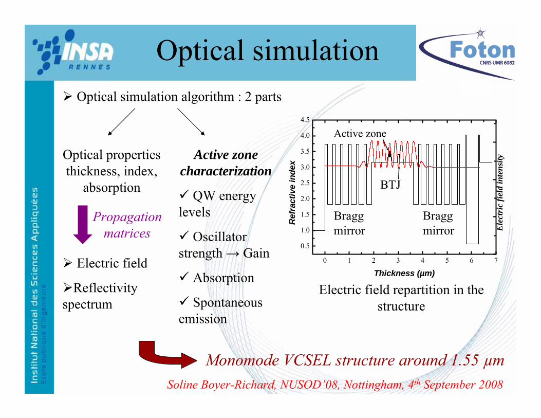
Optical simulation
0 1 2 3 4 5 6 7
0.5
1.0
1.5
2.0
2.5
3.0
3.5
4.0
4.5
Ref
ract
ive
inde
x
Thickness (µm)
Ele
ctri
c fie
ld in
tens
ity
Bragg mirror
Bragg mirror
Active zone
BTJ
Electric field repartition in the structure
Optical simulation algorithm : 2 parts
Optical properties thickness, index,
absorption
Propagation matrices
Electric field
Reflectivity spectrum
Active zone characterization
QW energy levels
Oscillator strength → Gain
Absorption
Spontaneous emission
Monomode VCSEL structure around 1.55 µm

Soline Boyer-Richard, NUSOD’08, Nottingham, 4th September 2008
Bragg mirrors2 types of Distributed Bragg Reflectors realized by magnetron sputtering :
InP
Miroir de Bragg 6 paires
a_SiNx/a_Si
Bragg mirror6 periods
InP
Miroir de Bragg 3.5 paires
a_SiNx/a_Si
Bragg mirror3.5 periods
Au
Simulation based on propagation matrices
Same reflectivity (99.6 %) @ 1.55 µm in good agreement with FTIR results
Total reflectivity of the VCSEL cavity : Free Spectral Range > 50 nm → monomode VCSEL
Standard DBRHybrid DBR
Design of InGaAs/InP1.55μm VCSELs
I- Introduction and context
II- Optical design of the VCSELsElectric field calculation
Bragg mirrors
III- Thermal analysis
IV- Buried Tunnel Junction
V- Conclusion
Soline Boyer-Richard, NUSOD’08, Nottingham, 4th September 2008

Soline Boyer-Richard, NUSOD’08, Nottingham, 4th September 2008
Thermal simulationVCSELs : Small active region → DBR → problem of heat dissipation
optical and electrical VCSEL thermal 2D finite element simulation
thermal resistance evaluation compared to experiment
Wavelenght shift as a function of pump power for optical VCSELs with standard or hybrid DBR.
10 20 30 40 50
1.566
1.568
1.570
1.572
1.574
1.576
1.578
1.580
1.582
0.22nm/mW
0.29nm/mW
Em
issi
on w
avel
engt
h (µ
m)
Pump power (mW)
conventional mirror hybrid mirror
Rth = 2.9 K/mW
Rth = 2.2 K/mW
Soline Boyer-Richard, NUSOD’08, Nottingham, 4th September 2008
Thermal simulation
Electrically pumped VCSEL 2D thermal
simulation.
0 1 2 3 4 5 6 7
1500
1600
1700
1800
1900
2000
2100
2200
2300
2400
Ther
mal
resi
stan
ce (K
/W)
InP thickness (µm)
Electrical VCSEL thermal resistance as a function of InP thickness (BTJ Ø 5 µm)
RTh = 2360 K/W for a 200 nm InP thickness VCSEL RTh = 2050 K/W (1 µm InP)
In
InPBragg mirror
Au
Active zone
Si3N4
Bragg mirror
InP
In
InPBragg mirror
Au
Active zone
Si3N4
Bragg mirror
InP
10 mW
Design of InGaAs/InP1.55μm VCSELs
I- Introduction and context
II- Optical design of the VCSELsElectric field calculation
Bragg mirrors
III- Thermal analysis
IV- Buried Tunnel Junction
V- Conclusion
Soline Boyer-Richard, NUSOD’08, Nottingham, 4th September 2008
Soline Boyer-Richard, NUSOD’08, Nottingham, 4th September 2008
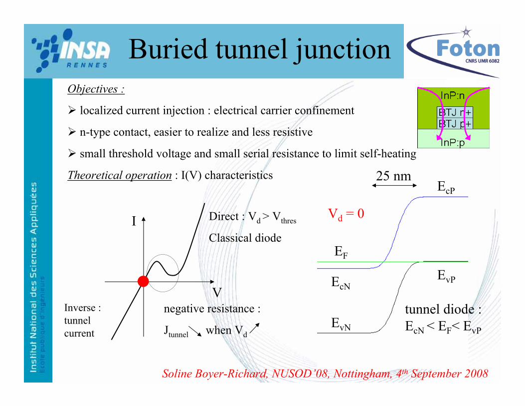
Objectives :
localized current injection : electrical carrier confinement
n-type contact, easier to realize and less resistive
small threshold voltage and small serial resistance to limit self-heating
Theoretical operation : I(V) characteristics
V
I
Inverse : tunnel current
Direct : Vd > Vthres
Classical diode
negative resistance :
Jtunnel when Vd
25 nm
Vd = 0
EvN
EcN
EcP
EvP
tunnel diode : EcN < EF< EvP
EF
Buried tunnel junction

Soline Boyer-Richard, NUSOD’08, Nottingham, 4th September 2008
Objectives :
localized current injection : electrical carrier confinement
n-type contact, easier to realize and less resistive
small threshold voltage and small serial resistance to limit self-heating
Theoretical operation : I(V) characteristics
V
I
Inverse : tunnel current
Direct : Vd > Vthres
Classical diode
negative resistance :
Jtunnel when Vd
Vd = -0.5 V
Buried tunnel junction
Jtunnel

Soline Boyer-Richard, NUSOD’08, Nottingham, 4th September 2008
Objectives :
localized current injection : electrical carrier confinement
n-type contact, easier to realize and less resistive
small threshold voltage and small serial resistance to limit self-heating
Theoretical operation : I(V) characteristics
V
I
Inverse : tunnel current
Direct : Vd > Vthres
Classical diode
negative resistance :
Jtunnel when Vd
Vd = 0.2 V
Buried tunnel junction
No tunnel currentVd<Vthres_diode
Soline Boyer-Richard, NUSOD’08, Nottingham, 4th September 2008
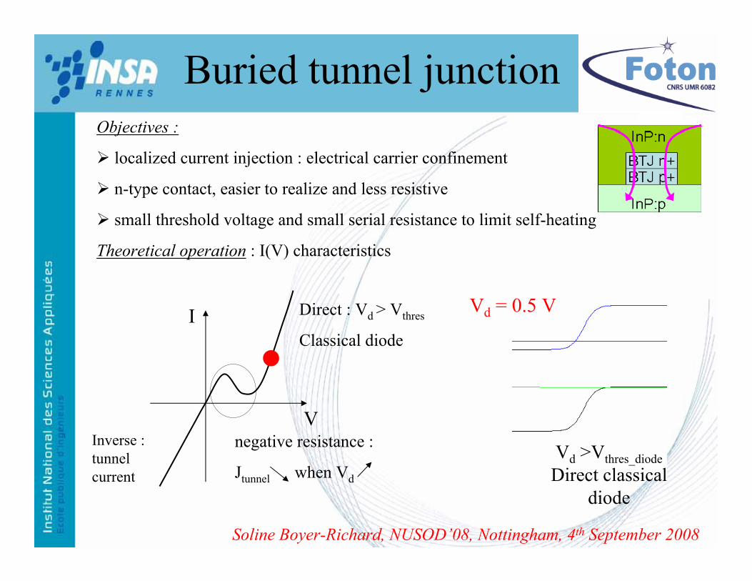
Objectives :
localized current injection : electrical carrier confinement
n-type contact, easier to realize and less resistive
small threshold voltage and small serial resistance to limit self-heating
Theoretical operation : I(V) characteristics
V
I
Inverse : tunnel current
Direct : Vd > Vthres
Classical diode
negative resistance :
Jtunnel when Vd
Vd = 0.5 V
Buried tunnel junction
Vd >Vthres_diodeDirect classical
diode
Soline Boyer-Richard, NUSOD’08, Nottingham, 4th September 2008
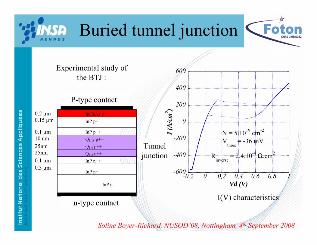
Buried tunnel junction
Jonction tunnel
Substrat InP n
Co ac c cu a e : / u
InP n++
InP p++
InGaAs p+ InP p+
InP n+
Q1.18 p++ Q1.4 p++ Q1.4 n++
0.2 µm 0.15 µm
0.1 µm 10 nm 25nm 25nm 0.1 µm 0.3 µm
Tunnel junction
P-type contact
n-type contact
Experimental study ofthe BTJ :
I(V) characteristics
-600
-400
-200
0
200
400
600
-0,2 0 0,2 0,4 0,6 0,8 1J
(A/c
m2 )
Vd (V)
N = 5.1019 cm-2
Vthres
= -36 mV
Rinverse
= 2.4.10-4 Ω.cm2
Soline Boyer-Richard, NUSOD’08, Nottingham, 4th September 2008
Buried tunnel junction1D Schrödinger-Poisson simulation useful to :
verify the tunnel effect in the reverse BTJ
avoid current leakage in the reverse InP junction outside the BTJ
-6
-5
-4
-3
-2
-1
0
Ene
rgy
(eV
)
Active ZoneQ1.18 153 nm
InP p+30 nm
BTJ
InP n
InP n
InP n
VB
VB
CB
CB
outside the BTJ
Simulation of the band diagram of the VCSEL in vertical direction, inside and outside the BTJ
-2 -1 0 1 2 3 4-2
-1
0
1
2
I (m
A)
V (V)
3944 BTJ:7µm 3944 without BTJ 4008 without BTJ 4008 BTJ:7µm
I(V) characteristics of the VCSEL cavities (without DBR)
3944 : 15 nm InP p+ leakage current
4008 : InP p+ = 240 nm …OK
Soline Boyer-Richard, NUSOD’08, Nottingham, 4th September 2008
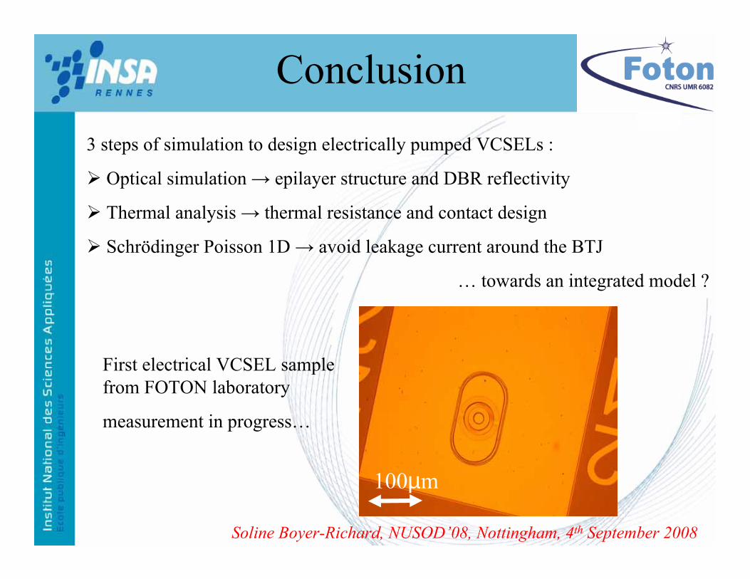
Conclusion3 steps of simulation to design electrically pumped VCSELs :
Optical simulation → epilayer structure and DBR reflectivity
Thermal analysis → thermal resistance and contact design
Schrödinger Poisson 1D → avoid leakage current around the BTJ
… towards an integrated model ?
100µm
First electrical VCSEL sample from FOTON laboratory
measurement in progress…