device&technology&for&gan3based&...
TRANSCRIPT
The Hong Kong University of Science and Technology
Kevin J. Chen PowerSOC’12 1
Device Technology for GaN-‐based Integrated Power Electronics
Kevin J. Chen The Hong Kong University of Science and Technology

The Hong Kong University of Science and Technology
Kevin J. Chen PowerSOC’12 2
Outline
• GaN’s benefits for power electronics • Technology challenges and soluDons
– Discrete power transistors – IntegraDon of power switches and recDfiers – Smart power ICs
• Summary

The Hong Kong University of Science and Technology
Kevin J. Chen PowerSOC’12 3
Trends in Power Converters
• High voltage, large capacity, high frequency • Compact size, smart control and low-‐cost • High-‐temperature operaDon and low-‐cost cooling systems
GaN Power Devices and ICs on Si
New semiconductor materials with fundamental advantages over Si: GaN and SiC

The Hong Kong University of Science and Technology
Kevin J. Chen PowerSOC’12 4
GaN: superior material properDes Physical Properties (Si) (GaAs) (4H-SiC) (GaN)
Bandgap (eV) 1.11 1.43 3.26 3.4 Thermal Cond. (W/cm⋅K )
1.5 0.46 3.5 1.5
Breakdown E-‐field (MV/cm)
0.3 0.3 2.5 2.5~3
e saturaDon velocity (×107cm/s)
1.0 2.0 2.0 2.5
e Mobility (cm2/V⋅s) 1300 5000 (2DEG)
600-900 2000 (2DEG)
BHFFOM* (µEc2) 1 9.5 45 98 *BHFFOM: Baliga’s high frequency figure of merit

The Hong Kong University of Science and Technology
Kevin J. Chen PowerSOC’12 5
GaN for Power Electronics Breaking the Si Limit
* N.-‐Q. Zhang, et al. IEDM Technical Digest, pp. 25.5.1 (2001).
n Lower loss, higher switching frequency, higher operaDng temperature
101 102 103 104 10510-2
10-1
100
101
102
103
4H-SiCLimit
AlGaN/GaN lateral limit
Si Limit
Spec
ific R O
N (mΩ
.cm
2 )
Breakdown Voltage (V)
GaN Limit
0 500 1000 1500
102
104
106
108
1010
1012
1014
Diamond/AlN
GaN6H SiCInNGaAs
Intri
nsic
Car
rier C
onc.
(cm
-3)
Temperature (oC)
Si

The Hong Kong University of Science and Technology
Kevin J. Chen PowerSOC’12 6
GaN and III-‐nitride: strong polarizaDon Charge PolarizaDon • Spontaneous • Piezoelectric
Commercial AlGaN/GaN-‐on-‐Si wafers: • Ga-‐face: PosiKve polarizaKon charges at the
AlGaN/GaN interface à high 2DEG density • Normally-‐on 2DEG channel without any
intenKonal doping
Ga-face
[0001]
N Ga
Substrate Negative Vth
Normally-on

The Hong Kong University of Science and Technology
Kevin J. Chen PowerSOC’12 7
Challenges for lateral AlGaN/GaN power HEMTs
• Gate control: normally-‐off operaKon, low gate leakage and large gate swing
• Surface passivaDon: low current collapse and low dynamic RON
• Buffer: low “OFF” state leakage, low trap state density and stress compensaKon/release
• Substrate: (111) Si -‐-‐-‐ how to integrate with Si CMOS (on (100) Si)?

The Hong Kong University of Science and Technology
Kevin J. Chen PowerSOC’12 8
GaN normally-‐off transistor technologies
Si Substrate
GaN Buffer2DEG
AlGaN BarrierS DPassivation
Gp-cap (AlGaN or GaN)
P-type cap
Si Substrate
GaN Buffer2DEG
AlGaN BarrierS DPassivationG
Si Substrate
GaN Buffer2DEG
AlGaN BarrierS DPassivation
GGate dielectric
Si Substrate
GaN Buffer2DEG
AlGaN Barrier
F
S DPassivation
G
Si Substrate
GaN Buffer2DEG
AlGaN Barrier
G
F
S DPassivation
Gate dielectric
Gate recess
Fluorine plasma ion implant.
HEMT MIS-HEMT
The Hong Kong University of Science and Technology
Kevin J. Chen PowerSOC’12 9
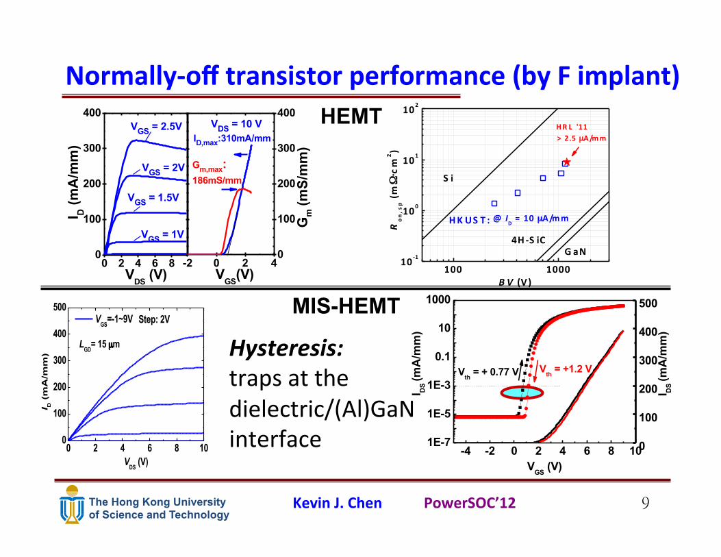
Normally-‐off transistor performance (by F implant)
0 2 4 6 80
100
200
300
400
-2 0 2 40
100
200
300
400
I D (m
A/m
m)
VDS (V)
VDS = 10 V
ID,max:310mA/mm
Gm,max:186mS/mm
VGS = 1V
VGS = 1.5V
VGS = 2V
VGS = 2.5V
Gm
(mS/
mm
)
VGS(V) 100 100010-‐1
100
101
102
@ ID = 10 µA/mm
> 2.5 µA/mmHR L '11
G aN4H-‐S iC
S i
Ron, s
p (mΩ⋅cm
2 )
B V (V )
HK US T :
-4 -2 0 2 4 6 8 101E-7
1E-5
1E-3
0.1
10
1000
Vth = + 0.77 V Vth = +1.2 V
I DS
(mA
/mm
)
VGS (V)
I DS
(mA
/mm
)
0
100
200
300
400
500
0 2 4 6 8 100
100
200
300
400
500
LGD= 15 µm
I D (
mA
/mm
)
VDS (V)
VGS=-1~9V Step: 2V
HEMT
MIS-HEMT
Hysteresis: traps at the dielectric/(Al)GaN interface

The Hong Kong University of Science and Technology
Kevin J. Chen PowerSOC’12 10
GaN buffer
i-AlGaNS G D
AlGaN/GaN HEMT
SiNx
Mechanisms of passivation Ø Surface states compensation --- charge balance Ø Field-plate: passivation enhancement by E-field modification
Si Substrate
GaN Buffer
i-AlGaN
Source Gate DrainSiNx/AlN
Surface passivaDon: current collapse reducDon

The Hong Kong University of Science and Technology
Kevin J. Chen PowerSOC’12 11
Current collapse reducDon – low dynamic RON
• R. Chu, et al., IEEE EDL, vol.32, p.632, 2011 • S. Huang, et al., IEEE EDL, vol. 33, p. 516, 2012
SiNx passivation PEALD-AlN passivation
The Hong Kong University of Science and Technology
Kevin J. Chen PowerSOC’12 12
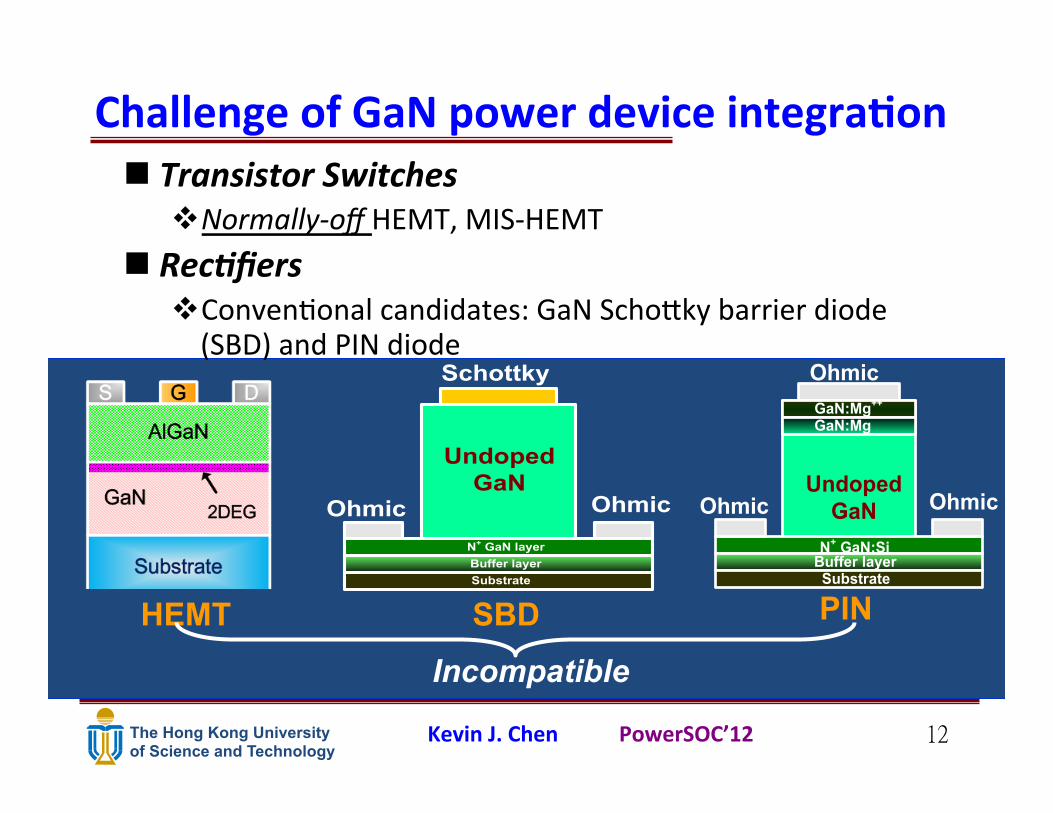
Challenge of GaN power device integraDon n Transistor Switches
v Normally-‐off HEMT, MIS-‐HEMT n RecFfiers
v ConvenKonal candidates: GaN Scho^ky barrier diode (SBD) and PIN diode
HEMT SBD PIN
Incompatible
Schottky
Undoped GaN
Ohmic OhmicN+ GaN layerBuffer layerSubstrate
Ohmic
Undoped GaNOhmic Ohmic
N+ GaN:SiBuffer layerSubstrate
GaN:Mg++
GaN:Mg
The Hong Kong University of Science and Technology
Kevin J. Chen PowerSOC’12 13
Silicon Substrate
GaN Buffer 2DEGAlGaN
F-
LOFF LAC
A C
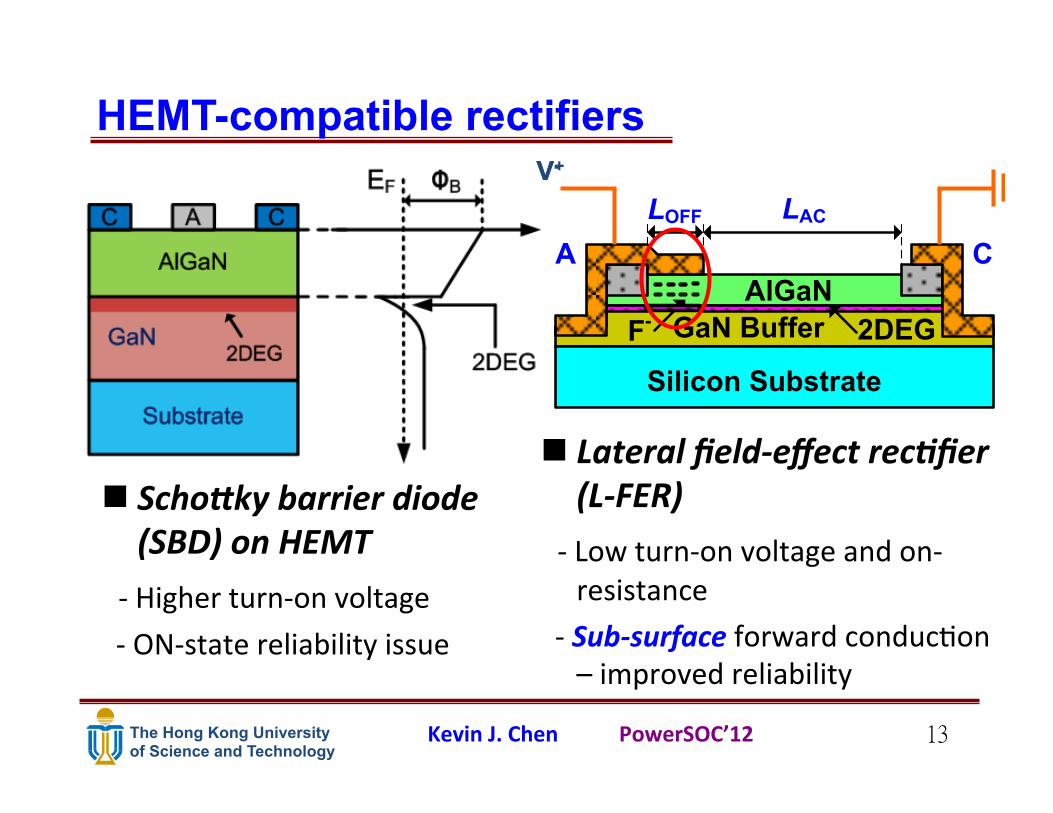
HEMT-compatible rectifiers V+ V-
n Lateral field-‐effect recFfier (L-‐FER)
-‐ Low turn-‐on voltage and on-‐resistance
-‐ Sub-‐surface forward conducKon – improved reliability
n SchoMky barrier diode (SBD) on HEMT
-‐ Higher turn-‐on voltage -‐ ON-‐state reliability issue
The Hong Kong University of Science and Technology
Kevin J. Chen PowerSOC’12 14
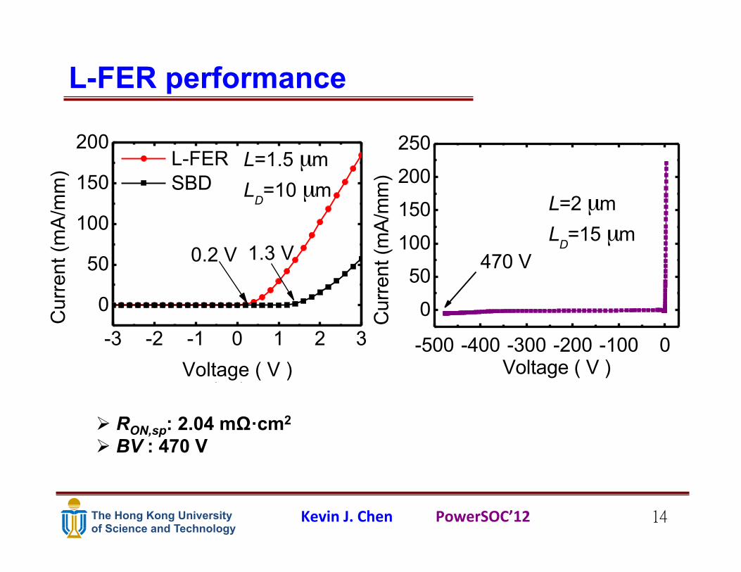
L-FER performance
Ø RON,sp: 2.04 mΩ·cm2 Ø BV : 470 V
-500 -400 -300 -200 -100 0
0
50
100
150
200
250
Cur
rent
(mA/
mm
)Voltage ( V )
L=2 µmLD=15 µm
470 V
-3 -2 -1 0 1 2 3
0
50
100
150
200
L-FER SBD
Cur
rent
(mA
/mm
)
Voltage ( V )
L=1.5 µmLD=10 µm
0.2 V 1.3 V
( a )

The Hong Kong University of Science and Technology
Kevin J. Chen PowerSOC’12 15
Monolithic integraDon of HEMT and L-‐FER
W. Chen, et al., APL, 2008, IEEE EDL 2009 W. Chen, et al., IEDM 2008.
+- 0V2.5V
Vout
Monolithic Integration
L
Normally-offHEMT
L-FER
C
VRec+ -
+
-VHEMT

The Hong Kong University of Science and Technology
Kevin J. Chen PowerSOC’12 16
GaN Smart Power IC Pladorm
Core power devices Peripheral devices
v Normally-‐off HEMT v Lateral Field-‐Effect RecDfier (L-‐FER)
Digital: All-‐n-‐channel direct-‐coupled FET logic (DCFL)
Analog: Sensing & ProtecDon
*K. Y. Wong et al. ISPSD’09

The Hong Kong University of Science and Technology
Kevin J. Chen PowerSOC’12 17
Performance of integrated devices
Well behaved devices within a wide range of operaDng temperature
0 2 4 6 80
50
100
150
200
250
300
350
400
-3 -2 -1 00
50
100
150
200
250
300
350
400
I D (m
A/m
m)
VDS (V)
Gm (m
S/m
m)
VGS (V)
VDS = 10V
D-mode25 oC
250 oCVGS = 0 V
-0.5 V
-1 V-1.5 V
VGS = 0 V
-0.5 V
-1 V
-1.5 V
25 OC
250 OC
(b)
0 1 2 30
50
100
150
200
250
300
350
-2 0 20
100200300
RT 50 oC 75 oC 100 oC 125 oC 150 oC 175 oC 200 oC 225 oC 250 oC 275 oC
Cur
rent
(mA
/mm
)
Voltage (V)
Voltage (V)
RTForward Voltage (V)
RT to 275oC25oC step
0 1 2 3 Forward Voltage (V)
350300250200150100500
I D(m
A/mm)
0 1 2 30
50
100
150
200
250
300
350
-2 0 20
100200300
RT 50 oC 75 oC 100 oC 125 oC 150 oC 175 oC 200 oC 225 oC 250 oC 275 oC
Cur
rent
(mA
/mm
)
Voltage (V)
Voltage (V)
RTForward Voltage (V)
RT to 275oC25oC step
0 1 2 3 Forward Voltage (V)
350300250200150100500
I D(m
A/mm)
0 2 4 6 80
50
100
150
200
250
300
350
400
-1 0 1 2 30
50
100
150
200
250
300
350
400E-mode
I D (m
A/m
m)
VDS (V)
VGS = 3 V
2.5 V
2 V
1.5 V
1 V
25 oC
250 oCVGS = 3 V
2.5 V
2 V
1.5 V1 V
VDS = 10V
Gm (m
S/m
m)
VGS (V)
25 OC
250 OC
L-FER

The Hong Kong University of Science and Technology
Kevin J. Chen PowerSOC’12 18 18
Digital IC : Direct-‐Coupled FET Logic
Proper operation: from room temp. to 350 oC (equipment limit)
* Y. Cai, et al. IEDM Technical Digest, (2005) and EDL, (2007).
350ºC VDD = 3.5V
Output Signal
DCFL Inverter17 Stage DCFL Ring Oscillator

The Hong Kong University of Science and Technology
Kevin J. Chen PowerSOC’12 19
Some basic GaN mixed-‐signal funcDonal blocks
VRef
VDD
Q 1
D 1
D 2
D 3
D 4
VSS
Voltage reference Bootstrap comparator
2-‐bit quanDzer
VDD
GND
Q Q
S R
600 μm
470 μm
flip-‐flop

The Hong Kong University of Science and Technology
Kevin J. Chen PowerSOC’12 20
Over-‐temperature protecDon IC VDD
M4M3
M1 M2
Ms
M5
Vo L-FER1
L-FER2
VOUT
VREF
VB
Temperature Sensor
Bootstrapped Comparator
* X. Liu et al. EDL, (2011). 50 100 150 200 250
4
6
8
10
12
V OU
T (V)
Temperature (oC)
VREF=2.25V VREF=2.15V VREF=2.05V VREF=1.95V VREF=1.85V
Tcrit

The Hong Kong University of Science and Technology
Kevin J. Chen PowerSOC’12 21
• GaN-‐on-‐Si power devices and ICs: an enabler for GaN-‐based PowerSOC – high efficiency, small size and simple thermal management
• IntegraKon of normally-‐off HEMTs and HEMT-‐compaDble field-‐effect recDfiers enables single-‐chip soluKon to switch-‐mode power converters.
• GaN smart power ICs with mixed-‐signal protecKon/control funcKons will enable more robust power converter soluKon.
Summary