digi board 2 - fbi.h-da.de · digitaltechnik / mikrocomputertechnik digital technology /...
TRANSCRIPT

Digitaltechnik / Mikrocomputertechnik Digital Technology / Microcomputer Technology
DIGI BOARD 2 Typ(e) 3910
Gerätebeschreibung
Technical Description

Digitaltechnik / Mikrocomputertechnik Digital Technology / Microcomputer Technology
hps SystemTechnik Lehr- + Lernmittel GmbH
Service-Adresse: Senden Sie das Gerät im Störungsfall mit einer möglichst genauen Fehlerbeschreibung an die un-tenstehende Adresse und geben Sie dazu Ihre An-schrift und Telefonnummer an. hps SystemTechnik Altdorfer Straße 16 88276 Berg Telefon: 07 51 / 5 60 75 70 Telefax: 07 51 / 5 60 75 77 Internet: www.hps-SystemTechnik.com E-mail: [email protected] Bestell-Nr.: V 3910 Alle Rechte, auch der Übersetzung, vorbehalten. Kein Teil des Werkes darf in irgendeiner Form (Druck, Fotokopie oder einem anderen Verfahren) ohne schriftliche Genehmigung von hps System-Technik reproduziert oder unter Verwendung elektronischer Systeme verarbeitet, vervielfältigt oder verbreitet werden. Hiervon sind die in §§ 53, 54 UrhG ausdrücklich genannten Ausnahmefälle nicht berührt.
Technische Änderungen vorbehalten.
Service Address: In case of malfunction please return the unit to the address mentioned below giving a detailed descrip-tion of the problem occurred and indicating your address and phone number. hps SystemTechnik Altdorfer Strasse 16 88276 Berg (Germany) Phone: +49 751 / 5 60 75 80 Telefax: +49 751 / 5 60 75 17 Internet: www.hps-SystemTechnik.com E-mail: [email protected]
Order No.: V 3910
All rights reserved. No part of this publication may be reproduced, transmitted, stored in a retrieval system, nor translated into any human or computer language, in any form or by any means, electronic, mechanical, magnetic, optical, chemical, manual orotherwise, without the prior permission of hps Sys-temTechnik.
Subject to technical modifications.
Code-Nr.: 0.1.3

DIGI BOARD 2 Typ(e) 3910 1
GB D Inhaltsverzeichnis 1 Allgemeines.............................1
2 Frontansicht des DIGI BOARD 2 (Typ 3910) ...............................2
3 Mechanische Daten...............17
4 Empfohlenes Zubehör ...........17
5 Erweiterungen .......................18
1 Allgemeines Das DIGI BOARD 2 wurde entwi-ckelt zur Vermittlung und Vertiefung von Grundlagenkenntnissen in der Digitaltechnik, der kontaktlosen Steuerungstechnik und der Mikro-computertechnik.
Alle Funktionsgruppen, die zur Durchführung von Versuchen in der Digitaltechnik benötigt werden, sind im DIGI BOARD 2 fest integriert und werden über ein eingebautes Netzteil mit Spannung versorgt.
Die Beschaltung der einzelnen Funktionsgruppen erfolgt über 2-mm-Verbindungstechnik.
Alle IC-Bausteine sind in Sockel eingesetzt.
Durch einfaches Einschrauben in eine BOX kann das DIGI BOARD 2 als mobile Trainingseinheit einge-setzt werden.
Contents 1 General ................................... 1
2 Front View of the DIGI BOARD 2 (Type 3910) ............................ 2
3 Mechanical Data ................... 17
4 Recommended Accessories.. 17
5 Expansions ........................... 18
1 General The DIGI BOARD 2 has been de-velopped for basic and further train-ing in the fundamentals of digital technology, non-contact control en-gineering and microcomputer tech-nology.
All the function groups required to conduct the experiments in digital technology are built into the DIGI BOARD 2 and are powered by an integrated power supply unit.
The individual function groups are connected in 2-mm connecting technology.
All IC components are inserted in sockets.
The DIGI BOARD 2 can also be used as mobile training unit simply by screwing it into a BOX.

2 DIGI BOARD 2 Typ(e) 3910
GB D
2 Frontansicht des DIGI BOARD 2 (Typ 3910) Front view of the DIGI BOARD (Type 3910)
DIGI BOARD 2 Typ(e) 3910 3
GB D (1) Netzanschluss • Netzspannung:
230 V AC / 115 V (110 V) AC, 50 ... 60 Hz, 30 VA
• Netzschalter: EIN/AUS mit Kontrollleuchte
• Netzsicherung: 400 mA T (230 V) 800 mA T (115 V)
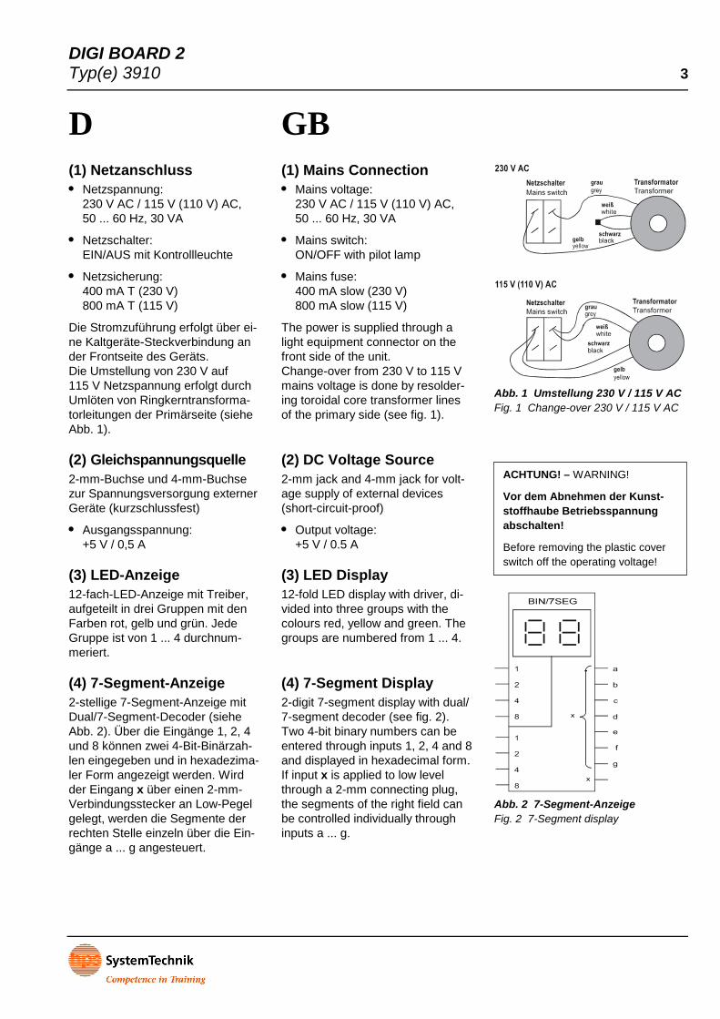
Die Stromzuführung erfolgt über ei-ne Kaltgeräte-Steckverbindung an der Frontseite des Geräts. Die Umstellung von 230 V auf 115 V Netzspannung erfolgt durch Umlöten von Ringkerntransforma-torleitungen der Primärseite (siehe Abb. 1).
(2) Gleichspannungsquelle 2-mm-Buchse und 4-mm-Buchse zur Spannungsversorgung externer Geräte (kurzschlussfest)
• Ausgangsspannung: +5 V / 0,5 A
(3) LED-Anzeige 12-fach-LED-Anzeige mit Treiber, aufgeteilt in drei Gruppen mit den Farben rot, gelb und grün. Jede Gruppe ist von 1 ... 4 durchnum-meriert.
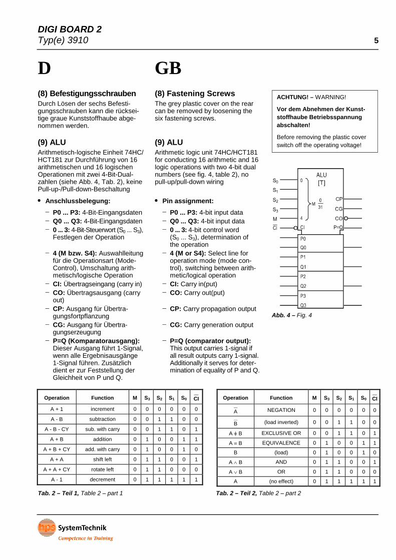
(4) 7-Segment-Anzeige 2-stellige 7-Segment-Anzeige mit Dual/7-Segment-Decoder (siehe Abb. 2). Über die Eingänge 1, 2, 4 und 8 können zwei 4-Bit-Binärzah-len eingegeben und in hexadezima-ler Form angezeigt werden. Wird der Eingang x über einen 2-mm-Verbindungsstecker an Low-Pegel gelegt, werden die Segmente der rechten Stelle einzeln über die Ein-gänge a ... g angesteuert.
(1) Mains Connection • Mains voltage:
230 V AC / 115 V (110 V) AC, 50 ... 60 Hz, 30 VA
• Mains switch: ON/OFF with pilot lamp
• Mains fuse: 400 mA slow (230 V) 800 mA slow (115 V)
The power is supplied through a light equipment connector on the front side of the unit. Change-over from 230 V to 115 V mains voltage is done by resolder-ing toroidal core transformer lines of the primary side (see fig. 1).
(2) DC Voltage Source 2-mm jack and 4-mm jack for volt-age supply of external devices (short-circuit-proof)
• Output voltage: +5 V / 0.5 A
(3) LED Display 12-fold LED display with driver, di-vided into three groups with the colours red, yellow and green. The groups are numbered from 1 ... 4.
(4) 7-Segment Display 2-digit 7-segment display with dual/7-segment decoder (see fig. 2). Two 4-bit binary numbers can be entered through inputs 1, 2, 4 and 8 and displayed in hexadecimal form. If input x is applied to low level through a 2-mm connecting plug, the segments of the right field can be controlled individually through inputs a ... g.
ACHTUNG! – WARNING!
Vor dem Abnehmen der Kunst-stoffhaube Betriebsspannung abschalten!
Before removing the plastic cover switch off the operating voltage!
Abb. 1 Umstellung 230 V / 115 V AC Fig. 1 Change-over 230 V / 115 V AC
Abb. 2 7-Segment-Anzeige Fig. 2 7-Segment display

4 DIGI BOARD 2 Typ(e) 3910
GB D (5) Adapterfelder Drei Adapterfelder zur Anpassung von 2-mm-Buchsen auf 4-mm-Buchsen
(6) GND 2-mm-Buchse und 4-mm-Buchse für Masse (GND) oder 0 V
(7) Adapter Zum Übergang von 2-mm-Verbin-dungstechnik auf 25-polige SUB-D-Steckverbindung, Pin 1 ... 13 und 18 sind belegt (Abb. 3, Tab. 1). Über diesen Adapter ist z.B. der Anschluss eines PCs möglich.
Pin Adresse Address
Bit Ein-/Ausgang Input/Output
Funktion Function
1 27AH 0 Ausgang/Output Strobe–––––––
2 278H 0 Ausgang/Output Data 1
3 278H 1 Ausgang/Output Data 2
4 278H 2 Ausgang/Output Data 3
5 278H 3 Ausgang/Output Data 4
6 278H 4 Ausgang/Output Data 5
7 278H 5 Ausgang/Output Data 6
8 278H 6 Ausgang/Output Data 7
9 278H 7 Ausgang/Output Data 8
10 279H 6 Eingang/Input ACK–––––
11 279H 7 Eingang/Input BUSY
12 279H 5 Eingang/Input Paper out
13 279H 4 Eingang/Input Select
18 – – – GND
(5) Adapter Fields Three adapter fields for adapting 2-mm jack to 4-mm jacks
(6) GND 2-mm jack and 4-mm jack for ground (GND) or 0 V
(7) Adapter For adapting 2-mm connection technique to 25-pin SUB-D connec-tor, pins 1 ... 13 and 18 are occu-pied (fig. 3, table 1). A PC for ex-ample can be connected through this adapter.
Abb. 3 – Fig. 3
ACHTUNG! – WARNING!
Mit den bei diesem Gerät einge-setzten Verbindungsleitungen und -steckern ist kein sicherer Berührungsschutz gewährleistet. Speisen Sie deshalb an den Buchsen niemals lebensgefährli-che Berührungsspannungen ein!
The connecting leads and plugs used with this unit do not safely guarantee protection against con-tact. Therefore, never feed shock-hazard voltages into the jacks!
Tab. 1 Centronics-Schnittstelle Table 1 Centronics interface
DIGI BOARD 2 Typ(e) 3910 5
GB D (8) Befestigungsschrauben Durch Lösen der sechs Befesti-gungsschrauben kann die rücksei-tige graue Kunststoffhaube abge-nommen werden.
(9) ALU Arithmetisch-logische Einheit 74HC/ HCT181 zur Durchführung von 16 arithmetischen und 16 logischen Operationen mit zwei 4-Bit-Dual-zahlen (siehe Abb. 4, Tab. 2), keine Pull-up-/Pull-down-Beschaltung • Anschlussbelegung:
− P0 ... P3: 4-Bit-Eingangsdaten − Q0 ... Q3: 4-Bit-Eingangsdaten − 0 ... 3: 4-Bit-Steuerwort (S0 ... S3),
Festlegen der Operation
− 4 (M bzw. S4): Auswahlleitung für die Operationsart (Mode-Control), Umschaltung arith-metisch/logische Operation
− CI: Übertragseingang (carry in) − CO: Übertragsausgang (carry
out) − CP: Ausgang für Übertra-
gungsfortpflanzung − CG: Ausgang für Übertra-
gungserzeugung − P=Q (Komparatorausgang):
Dieser Ausgang führt 1-Signal, wenn alle Ergebnisausgänge 1-Signal führen. Zusätzlich dient er zur Feststellung der Gleichheit von P und Q.
Operation Function M S3 S2 S1 S0 CI––
A + 1 increment 0 0 0 0 0 0
A - B subtraction 0 0 1 1 0 0
A - B - CY sub. with carry 0 0 1 1 0 1
A + B addition 0 1 0 0 1 1
A + B + CY add. with carry 0 1 0 0 1 0
A + A shift left 0 1 1 0 0 1
A + A + CY rotate left 0 1 1 0 0 0
A - 1 decrement 0 1 1 1 1 1
Operation Function M S3 S2 S1 S0 CI––
A––
NEGATION 0 0 0 0 0 0
B––
(load inverted) 0 0 1 1 0 0
A ≡ B EXCLUSIVE OR 0 0 1 1 0 1
A ≡ B EQUIVALENCE 0 1 0 0 1 1
B (load) 0 1 0 0 1 0
A ∧ B AND 0 1 1 0 0 1
A ∨ B OR 0 1 1 0 0 0
A (no effect) 0 1 1 1 1 1
(8) Fastening Screws The grey plastic cover on the rear can be removed by loosening the six fastening screws.
(9) ALU Arithmetic logic unit 74HC/HCT181 for conducting 16 arithmetic and 16 logic operations with two 4-bit dual numbers (see fig. 4, table 2), no pull-up/pull-down wiring • Pin assignment:
− P0 ... P3: 4-bit input data − Q0 ... Q3: 4-bit input data − 0 ... 3: 4-bit control word
(S0 ... S3), determination of the operation
− 4 (M or S4): Select line for operation mode (mode con-trol), switching between arith-metic/logical operation
− CI: Carry in(put) − CO: Carry out(put)
− CP: Carry propagation output
− CG: Carry generation output
− P=Q (comparator output):
This output carries 1-signal if all result outputs carry 1-signal. Additionally it serves for deter-mination of equality of P and Q.
ACHTUNG! – WARNING!
Vor dem Abnehmen der Kunst-stoffhaube Betriebsspannung abschalten!
Before removing the plastic cover switch off the operating voltage!
Abb. 4 – Fig. 4
Tab. 2 – Teil 1, Table 2 – part 1 Tab. 2 – Teil 2, Table 2 – part 2

6 DIGI BOARD 2 Typ(e) 3910
GB D (10) Einerkomplement Mit diesem Baustein (Abb. 5) kann eine 4-Bit-Binärzahl invertiert wer-den. Wird der Steuereingang EN2 von Low- auf High-Pegel geschal-tet, erscheint die an den Eingängen angelegte 4-Bit-Binärzahl an den Ausgängen invertiert.
(11) Schieberegister Bidirektionales 4-Bit-Schieberegis-ter mit Parallel- und Seriell-Betrieb (Abb. 6), positiv flankengetriggert, rechts- und linksschiebend
• Anschlussbelegung: − R: statischer Rücksetzein-
gang, aktiv mit Low-Pegel − C4/1→/2←: Takteingang für
Schieben (links/rechts) und pa-rallele Dateneingabe je nach gewähltem Modus (0 ... 3)
− 1,4D: serieller Eingang nach rechts schieben
− 2,4D: serieller Eingang nach links schieben
− 3,4D: Eingänge für Parallel-schieben
Hinweis: Die erste Ziffer an den Eingängen gibt den Betriebsmodus an.
Die beiden Adressleitungen S0 und S1 in Tab. 3 legen jeweils den Ar-beitsmodus (Mode) fest.
Mode S0 S1 Function
0 0 0 no function
1 1 0 serial input, shift to right
2 0 1 serial input, shift to left
3 1 1 parallel input
Mode S0 S1 Funktion
0 0 0 keine Funktion
1 1 0 serieller Eingang,rechts schieben
2 0 1 serieller Eingang,links schieben
3 1 1 parallele Eingabe
(10) One's Complement A 4-bit binary number can be in-verted with this component (fig. 5). If the control input EN2 is switched from low to high level, the 4-bit bi-nary number applied to the inputs appears inverted at the outputs.
(11) Shift Register Bidirectional 4-bit shift register with parallel and serial operation (fig. 6), positive edge triggered, right and left shift
• Pin assignment: − R: static reset input, active
with low level − C4/1→/2←: Clock input for
shift (left/right) and parallel data input depending on the selected mode (0 ... 3)
− 1,4D: Serial input for right shift
− 2,4D: Serial input for left shift
− 3,4D: Inputs for parallel shift
Note: The first digit at the inputs indicates the operating mode.
The two address lines S0 and S1 in table 3 determine the operation mode respectively.
Abb. 5 Einerkomplement Fig. 5 One's complement
Abb. 6 4-Bit-Schieberegister Fig. 6 4-bit shift register
Tab. 3 Table 3
DIGI BOARD 2 Typ(e) 3910 7
GB D (12) Demultiplexer 4-Kanal-Demultiplexer mit zwei Ein-gängen, davon einer invertiert (siehe Abb. 7). Tab. 4 zeigt die Belegung der Steuereingänge A0 und A1 für den jeweiligen Ausgangskanal.
(13) Multiplexer 4-Kanal-Multiplexer mit zusätzlich invertiertem Ausgang (Abb. 8). Tab. 4 zeigt die Belegung der Steu-ereingänge A0 und A1 für den je-weiligen Eingangskanal. Liegt am Eingang EN
––––– High-Pegel,
wird die Ausgabe des Multiplexers gestoppt. Durch einen Low-Pegel erfolgt die Freigabe des Multiple-xers.
(14) DA-Wandler 4-Bit-DA-Wandler (siehe Abb. 9)
• Ausgangsspannung: 0 ... 5 V DC
• Auflösung: ca. 312 mV
(15) AD-Wandler 4-Bit-AD-Wandler (siehe Abb. 10) mit SOC-Eingang und EOC-Aus-gang. Der Start der AD-Umsetzung erfolgt durch einen positiven Impuls am SOC-Eingang (start of conver-sation). Das Ende der AD-Umset-zung kann mit dem EOC-Ausgang (end of conversation) sichtbar ge-macht werden. Es erscheint dabei ein kurzer Nadelimpuls. Er kann entweder mit einem Speicheroszil-loskop angezeigt oder über das Monoflop des DIGI BOARD 2 ver-längert und über eine LED sichtbar gemacht werden.
• Eingangsspannung: 0 ... 5 V DC
• Auflösung: ca. 312 mV
• Umsetzungszeit: ca. 100 µs
A0 A1 Kanal Channel
0 0 0
0 1 1
1 0 2
1 1 3
(12) Demultiplexer 4-channel demultiplexer with two in-puts one of which is inverted (see fig. 7). Table 4 shows the assign-ment of the control inputs A0 and A1for the respective output channel.
(13) Multiplexer 4-channel multiplexer with addition-ally inverted output (fig. 8). Table 4 shows the assignment of the con-trol inputs A0 and A1 for the re-spective input channel. If high level is applied to input EN
–––––
the multiplexer output is stopped. The multiplexer is enabled by a low level.
(14) DA Converter 4-bit DA converter (see fig. 9)
• Output voltage: 0 ... 5 V DC
• Resolution: approx. 312 mV
(15) AD Converter 4-bit AD converter (see fig. 10) with SOC input and EOC output. The AD conversion is started by a posi-tive pulse at the SOC input (start of conversion). The end of the AD conversion can be made visible by the EOC output (end of conver-sion). A short needle pulse ap-pears. It can be displayed either with a storage oscilloscope or lengthened by the monoflop of the DIGI BOARD 2 and made visible by a LED.
• Input voltage: 0 ... 5 V DC
• Resolution: approx. 312 mV
• Conversion time: approx. 100 µs
Abb. 7 Fig. 7 Tab. 4 – Table 4
Abb. 8 – Fig. 8
Abb. 10 – Fig. 10
Abb. 9 – Fig. 9
8 DIGI BOARD 2 Typ(e) 3910
GB D (16) Addierer Zwei Volladdierer (4 Bit) mit Über-tragseingang (CI = Carry in) und Übertragsausgang (CO = Carry out) zur Addition von zwei 4-Bit-Dual-zahlen (siehe Abb. 11). Wird das Ergebnis > F, so muss am Über-tragsausgang der Zustand von Low auf High wechseln. Wird an den Übertragseingang ein High-Pegel gelegt, so erhöht sich das Ergebnis um „1“.
(17) 4-Bit-Komparator Komparator zum Vergleich von zwei 4-Bit-Dualzahlen (Abb. 12) mit Kaskadierungseingängen (>, =, <). Die Kaskadierungseingänge sind im Gegensatz zu den P- und Q-Ein-gängen nicht mit Pull-up-Widerstän-den beschaltet. Es besteht zusätz-lich die Möglichkeit, zwei 5-Bit-Dual-zahlen miteinander zu vergleichen, indem die Ausgänge des 1-Bit-Komparators (siehe Punkt 21) auf die Kaskadierungseingänge des 4-Bit-Komparators aufgeschaltet werden. Die Eingänge des 1-Bit-Komparators werden dabei zusätz-lich benutzt.
(18) Schmitt-Trigger Zwei invertierende Schmitt-Trigger, keine Pull-up-/Pull-down-Beschal-tung, auch als Inverter einsetzbar (Abb. 13). Werden die Schmitt-Trigger z.B. am Eingang mit der Gleichspannungs-Signalquelle (sie-he Punkt 26) beschaltet, kann die Schalthysterese aufgezeigt werden.
(19) Modul-Steckfeld Zwei Steckfelder mit je zwei 4-mm-Buchsen (Steckerabstand: 57 mm) zur Aufnahme von zusätzlichen steckbaren Modulen (Serie 9400)
• Versorgungsspannung: 5 V DC / max. 1 A (kurzschlussfest)
(16) Adder Two full adders (4 bits) with carry in (CI) and carry out (CO) for addition of two 4-bit dual numbers (see fig. 11). If the result becomes > F, the state must change from low to high at the carry output. If a high level is applied to the carry input, the result is incre-mented by „1“.
(17) 4-Bit Comparator Comparator for comparing two 4-bit dual numbers (fig. 12) with cascad-ing inputs (>, =, <). The cascading inputs are not wired with pull-up re-sistors in opposition to the P and Q inputs. It is also possible to compare two 5-bit dual numbers by connect-ing the outputs of the 1-bit compara-tor (see item 21) to the cascading inputs of the 4-bit comparator. The inputs of the 1-bit comparator are then used additionally.
(18) Schmitt Trigger Two inverting Schmitt triggers, no pull-up/pull-down wiring, can also be used as inverters (fig. 13). The switching hysteresis can be shown for example if the Schmitt triggers are connected to the DC voltage signal source (see item 26) on the input side.
(19) Module Connector Field Two connector fields with two 4-mm jacks each (plug spacing: 57 mm) for plugging in additional modules (series 9400)
• Voltage supply: 5 V DC / max. 1 A (short-circuit-proof)
Abb. 11 – Fig. 11
Abb. 12 – Fig. 12
Abb. 13 – Fig. 13

DIGI BOARD 2 Typ(e) 3910 9
GB D (20) Inverter Zwei Inverter mit offenem Kollektor und hinzuschaltbaren Pull-up-Wider- ständen (Abb. 14, Tab. 5). Wird an die Eingänge der beiden Inverter Low-Pegel gelegt, liefern beide Aus-gänge nur dann High-Pegel, wenn der Pull-up-Widerstand über einen 2-mm-Verbindungsstecker gesteckt ist.
(21) 1-Bit-Komparator Komparator mit zwei Eingängen und drei Ausgängen zum Vergleich von zwei 1-Bit-Dualzahlen (siehe Abb. 15, Tab. 6). Die Eingänge sind nicht mit Pull-up-/Pull-down-Wider-ständen beschaltet. In Verbindung mit dem 4-Bit-Komparator können zwei 5-Bit-Dualzahlen miteinander verglichen werden (siehe Punkt 17).
(22) Äquivalenz Äquivalenzglied bzw. Gleichwertig-keitsgatter mit zwei Eingängen und einem Ausgang (siehe Abb. 16, Tab. 7). Die Eingänge sind nicht mit Pull-up-/Pull-down-Widerständen beschaltet.
(23) Antivalenz Antivalenzglied bzw. EXKLUSIV-ODER-Gatter mit zwei Eingängen und einem Ausgang (siehe Abb. 17, Tab. 8). Die Eingänge sind nicht mit Pull-up-/ Pull-down-Widerständen beschaltet.
(24) Monoflop Positiv flankengetriggertes Mono-flop mit Schmitt-Trigger-Eingang (nicht nachtriggerbar), invertiertem und nichtinvertiertem Ausgang (sie-he Abb. 18). Über einen 2-mm-Verbindungsstecker sind folgende Zeiten programmierbar: 0,1 s, 1 s, 5 s. Das Monoflop funktioniert nur dann, wenn eine der drei angege-benen Zeiten programmiert ist.
A Q
0 1
1 0
P Q P > Q P < Q P = Q
0 0 0 0 1
0 1 0 1 0
1 0 1 0 0
1 1 0 0 1
A B Q
0 0 1
0 1 0
1 0 0
1 1 1
A B Q
0 0 0
0 1 1
1 0 1
1 1 0
(20) Inverters Two inverters with open collector and connectable pull-up resistors (fig. 14, table 5). If low level is ap-plied to the inputs of the two invert-ers, both the outputs only supply high level if the pull-up resistor is connected via a 2-mm connecting plug.
(21) 1-Bit Comparator Comparator with two inputs and three outputs for comparing two 1-bit dual numbers (see fig. 15, table 6). The inputs are not wired with pull-up/pull-down resistors. Two 5-bit dual numbers can be compared in combination with the 4-bit comparator (see item 17).
(22) Equivalence Equivalence element or equality gate with two inputs and one output (see fig. 16, table 7). The inputs are not wired with pull-up/pull-down re-sistors.
(23) Antivalence Antivalence element or EXCLU-SIVE OR gate with two inputs and one out-put (see fig. 17, table 8). The inputs are not wired with pull-up/pull-down resistors.
(24) Monoflop Positive edge triggered monoflop with Schmitt trigger input (non-retriggerable), inverted and non-inverted output (see fig. 18). The following times can be programmed by means of a 2-mm connecting plug: 0.1 s, 1 s, 5 s. The function of the monoflop is only guaranteed, if one of the three times is pro-grammed.
Abb. 14 – Fig. 14
Tab. 5 – Table 5
Abb. 15 – Fig. 15
Tab. 6 – Table 6
Abb. 16 – Fig. 16
Abb. 17 – Fig. 17
Abb. 18 – Fig. 18
Tab. 7 – Table 7
Tab. 8 – Table 8
10 DIGI BOARD 2 Typ(e) 3910
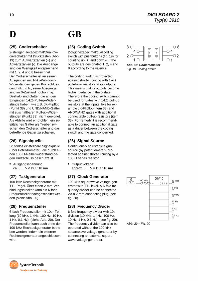
GB D (25) Codierschalter 2-stelliger Hexadezimal/Dual-Co-dierschalter mit Drucktasten (Abb. 19) zum Aufwärtszählen (+) und Abwärtszählen (-). Die Ausgänge sind der Wertigkeit entsprechend mit 1, 2, 4 und 8 bezeichnet. Der Codierschalter ist an seinen Ausgängen mit 1-kΩ-Pull-down-Widerständen gegen Kurzschluss geschützt, d.h., seine Ausgänge sind im 0-Zustand hochohmig. Deshalb sind Gatter, die an den Eingängen 1-kΩ-Pull-up-Wider-stände haben, wie z.B. JK-Flipflop (Punkt 38) und UND/NAND-Gatter mit zuschaltbaren Pull-up-Wider-ständen (Punkt 33), nicht geeignet. Als Abhilfe wird empfohlen, ein zu-sätzliches Gatter als Treiber zwi-schen den Codierschalter und das betreffende Gatter zu schalten.
(26) Signalquelle Stufenlos einstellbare Signalquelle (über Potenziometer), die durch ei-nen 100-Ω-Reihenwiderstand ge-gen Kurzschluss geschützt ist.
• Ausgangsspannung: ca. 0 ... 5 V DC / 10 mA
(27) Taktgenerator 100-kHz-Rechteckgenerator mit TTL-Pegel. Über einen 2-mm-Ver-bindungsstecker kann ein 6-fach Frequenzteiler nachgeschaltet wer-den (siehe Abb. 20).
(28) Frequenzteiler 6-fach Frequenzteiler mit 10er-Tei-lung (10 kHz, 1 kHz, 100 Hz, 10 Hz, 1 Hz, 0,1 Hz), (siehe Abb. 20). Der Frequenzteiler kann auch ohne den 100-kHz-Rechteckgenerator betrie-ben werden, indem ein externer Rechteckgenerator angeschlossen wird.
(25) Coding Switch 2-digit hexadecimal/dual coding switch with pushbuttons (fig. 19) for counting up (+) and down (-). The outputs are designated 1, 2, 4 and 8 according to the valence. The coding switch is protected against short-circuiting with 1-kΩ pull-down resistors at its outputs. This means that its outputs become high-impedance in the 0-state. Therefore the coding switch cannot be used for gates with 1-kΩ pull-up resistors at the inputs, like for ex-ample JK-Flipflop (item 38) and AND/NAND gates with additional connectable pull-up resistors (item 33). For remedy it is recommend-able to connect an additional gate as a driver between the coding switch and the gate concerned.
(26) Signal Source Continuously adjustable signal source (by potentiometer), pro-tected against short-circuiting by a 100-Ω series resistor.
• Output voltage: approx. 0 ... 5 V DC / 10 mA
(27) Clock Generator 100-kHz squarewave voltage gen-erator with TTL level. A 6-fold fre-quency divider can be connected via a 2-mm connecting plug (see fig. 20).
(28) Frequency Divider 6-fold frequency divider with 10s division (10 kHz, 1 kHz, 100 Hz, 10 Hz, 1 Hz, 0.1 Hz), (see fig. 20). The frequency divider can also be operated without the 100-kHz squarewave voltage generator by connecting an external square-wave voltage generator.
Abb. 19 Codierschalter Fig. 19 Coding switch
Abb. 20 – Fig. 20

DIGI BOARD 2 Typ(e) 3910 11
GB D (29) Taster Prellfreier Taster mit den Ausgän-gen Q und Q
—. Wird der Taster betä-
tigt, liegt am Ausgang Q High-Pegel und am Ausgang Q
— Low-Pegel.
(30) High/Low-Buchsen 2-mm-Buchsen zum Abgriff von High- und Low-Zuständen. Alle High-Ausgänge sind über 120-Ω-Reihenwiderstände (siehe Abb. 21) gegen Kurzschluss geschützt.
(31) Eingabetastatur Zwei Eingabetastaturen mit jeweils vier Tastenpaaren zur Erzeugung und Rücksetzung von High- und Low-Zuständen. Durch Gedrückthal-ten der Taste L und gleichzeitigem Drücken der Taste H, kann „getas-tet“ werden. Die Anzeige der High-Zustände erfolgt über rote LEDs.
(32) UND/NAND-Gatter Sieben UND/NAND-Gatter mit je vier Eingängen, nichtinvertiertem und invertiertem Ausgang (siehe Abb. 22). Die Eingänge liegen an Pull-up-Widerständen. Um eine si-chere Funktion zu gewährleisten, müssen deshalb nicht alle Eingän-ge des Gatters beschaltet sein. Wird nur ein Eingang beschaltet, kann das Gatter auch als Inverter eingesetzt werden.
(33) UND/NAND-Gatter mit Pull-up-Widerständen
UND/NAND-Gatter mit drei Eingän-gen und zusätzlich zuschaltbaren Pull-up-Widerständen (über 2-mm-Verbindungsstecker), nichtinvertier-tem und invertiertem Ausgang (sie-he Abb. 23). Ist der Pull-up-Wider-stand nicht angeschlossen, sind die Eingänge unbeschaltet und es kön-nen Störungen auftreten, da kein definierter Zustand vorliegt.
(29) Pushbutton Bounce-free pushbutton with the outputs Q and Q
—. When the push-
button is pressed, high level is ap-plied to output Q and low level to output Q
—.
(30) High/Low Jacks 2-mm jacks for tapping high and low states. All high outputs are pro-tected against short-circuiting by 120-Ω series resistors (see fig. 21).
(31) Input Keyboard Two input keyboards with four pairs of keys each for generating and re-setting high and low states. When key L is kept pressed and you press key H at the same time, „keying“ is allowed. The high states are indi-cated by red LEDs.
(32) AND/NAND Gate Seven AND/NAND gates with four inputs each, non-inverting and in-verting output (see fig. 22). The in-puts are applied to pull-up resistors, therefore not all inputs of the gate need to be connected to guarantee a reliable function. If only one input is connected, the gate can also be used as an inverter.
(33) AND/NAND Gate with Pull-up Resistors
AND/NAND gate with three inputs and additional connectable pull-up resistors (by 2-mm connecting plugs), non-inverted and inverted output (see fig. 23). If the pull-up resistor is not connected, the inputs are not connected and disturbances may occur because no defined state exists.
Abb. 21 – Fig. 21
Abb. 22 – Fig. 22
Abb. 23 – Fig. 23

12 DIGI BOARD 2 Typ(e) 3910
GB D (34) ODER/NOR-Gatter Fünf ODER/NOR-Gatter mit je vier Eingängen, nichtinvertiertem und invertiertem Ausgang (siehe Abb. 24). Die Eingänge liegen an Pull-down-Widerständen. Um eine si-chere Funktion zu gewährleisten, müssen deshalb nicht alle Eingän-ge des Gatters beschaltet sein. Wird nur ein Eingang beschaltet, kann das Gatter auch als Inverter eingesetzt werden.
(35) ODER/NOR-Gatter mit Pull-down-Wider-ständen
ODER/NOR-Gatter mit drei Ein-gängen und zuschaltbaren Pull-down-Widerständen, nichtinvertier-tem und invertiertem Ausgang (sie-he Abb. 25). Werden nicht alle Ein-gänge verwendet, müssen über ei-nen 2-mm-Verbindungsstecker die Pull-down-Widerstände zugeschal-tet werden.
(36) Kombigatter Drei UND/ODER-Kombinationsgat-ter, wobei die UND-Gatter je zwei Eingänge besitzen, die an Pull-up-Widerständen liegen. Das ODER-Gatter besitzt einen nichtinvertier-ten und einen invertierten Ausgang (siehe Abb. 26). Das Kombigatter kann auch als UND-Gatter mit zwei Eingängen verwendet werden, in-dem die Eingänge eines der bei-den Gatter an Low-Pegel gelegt werden. Wird das Kombigatter als ODER-Gatter mit zwei Eingängen eingesetzt, verwendet man nur je-weils einen Eingang der UND-Gat-ter, die beiden anderen bleiben un-beschaltet.
(34) OR/NOR Gate Five OR/NOR gates with four in-puts each, non-inverted and inver-ted output (see fig. 24). The inputs are applied to pull-down resistors, therefore not all inputs of the gate need to be connected to guarantee a reliable function. If only one input is connected, the gate can also be used as an inverter.
(35) OR/NOR Gate with Pull-down Resistors
OR/NOR gate with three inputs and connectable pull-down resis-tors, non-inverted and inverted out-put (see fig. 25). If not all inputs are used, the pull-down resistors must be connected by a 2-mm connecting plug.
(36) Combi Gate Three AND/OR combination gates, whereby the AND gates have two inputs each which are connected to pull-up resistors. The OR gate has a non-inverted and an inverted out-put (see fig. 26). The combigate can also be used as an AND gate with two inputs by applying the in-puts of one of the two gates to low level. If the combi gate is used as an OR gate with two inputs, only one input respectively of the AND gates is used, the other two remain unconnected.
Abb. 24 – Fig. 24
Abb. 25 – Fig. 25
Abb. 26 – Fig. 26

DIGI BOARD 2 Typ(e) 3910 13
GB D (37) D-Flipflop Vier einzustandsgesteuerte D-Flip-flops mit nichtinvertierten und inver-tierten Ausgängen (siehe Abb. 27, Tab. 9). Der am Eingang 1D anlie-gende Zustand wird am Taktein-gang C1 übernommen und an den nichtinvertierten Ausgang Q1 über-geben. Der nichtinvertierte Ausgang hat immer den entgegengesetzten Zustand des invertierten Ausgangs Q2. Die hier verwendeten D-Flip-flops werden häufig als Binär-Spei-cherelemente eingesetzt.
(38) JK-Flipflop Vier zweiflankengesteuerte JK-Flip-flops mit nichtinvertierten und inver-tierten Ausgängen (siehe Abb. 28, Tab. 10). Mit dem Set-Eingang S und dem Reset-Eingang R lässt sich das Flipflop setzen und rück-setzen. Ist nur der 1J- und der 1K-Eingang beschaltet, werden die Zustände an diesen Eingängen bei jeder negati-ven Taktflanke am Takteingang C1 an die Ausgänge übergeben (nega-tiv flankengetriggert). Ist nur der Takteingang beschaltet, kippt das Flipflop bei jeder negativen Takt-flanke.
• tn: Zustand vor dem Takt- impuls
• tn+1: Zustand nach dem Takt- impuls
• x: Zustand ändert sich nicht
• y: Zustand hat sich nach dem Taktimpuls geändert
Die JK-Flipflops können auch als RS-Flipflops in verschiedenen Vari-anten eingesetzt werden.
Takt Clock
1D Q1 Q2
1 0 0 1
1 1 1 0
tn tn+1
J K Q1 Q2
0 0 x x
0 1 0 1
1 0 1 0
1 1 y y
(37) D-Flipflop Four one-state controlled D-flipflops with non-inverted and inverted out-puts (see fig. 27, table 9). The state at input 1D is accepted at the clock input C1 and delivered to the non-inverted output Q1. The non-in-verted output always has the state opposite to that of the inverted out-put Q2. The D-flipflops used here are often used as binary memory components.
(38) JK-Flipflop Four two-edge controlled JK-flip-flops with non-inverted and inverted outputs (see fig. 28, table 10). The flipflop can be set and reset with the set input S and the reset input R. If only the 1J and 1K inputs are wired, the states at these inputs are transferred to the outputs with every negative clock edge at clock input C1 (negative edge triggered). If only the clock input is connected, the flipflop is activated with every negative clock edge.
• tn: State before the clock pulse
• tn+1: State after the clock pulse
• x: State does not change
• y: State has changed after the clock pulse
The JK-flipflops can also be used as RS-flipflops in various variants.
Tab. 10 – Table 10
Tab. 9 – Table 9
Abb. 28 – Fig. 28
Abb. 27 – Fig. 27

14 DIGI BOARD 2 Typ(e) 3910
GB D (39) Binärzähler Synchroner 4-Bit-Vorwärts-/Rück-wärts-Binärzähler (siehe Abb. 29)
• Anschlussbelegung: − CT=0: Wird an diesen Ein-
gang Low-Pegel gelegt, wird der Zähler zurückgesetzt; mit einem High-Pegel wird der Zähler aktiviert.
− 2+/G1: Takteingang für Vor-wärtszähler. Eingang G2, ist im unbeschalteten Zustand positiv.
− 1-/G2: Takteingang für Rück-wärtszähler. Eingang G1 ist positiv.
− C3: Wird an den Ladeeingang C3 ein Low-Pegel gelegt, ü-bernimmt der Zähler die anlie-gende Bitkombination an den Ausgang. Der Ladevorgang ist unabhängig vom Takt 2+/G1 oder 1-/G2.
− 3D: Eingänge für 4-Bit-Binär-zahl
− 1—
CT=15: Dieser Ausgang wechselt bei Erreichen der Hexadezimal-Zahl F von High- auf Low- Pegel.
− 2—
CT=0: Der Ausgang wechselt bei Erreichen der Hexadezi-mal-Zahl „0“ von High- auf Low-Pegel.
(40) RAM 8 x 4 Statisches RAM (S-RAM) mit 8 Ad-ressen (0 ... 7) und 4 Bit Datenbrei-te (siehe Abb. 30)
• Anschlussbelegung: − 0, 1, 2: Adresseingänge 0 ... 7 − WE: Write enable (Schreib-
freigabe) − OE: Output enable (Lesefrei-
gabe) − CS: Chip select (CS
—— = 0, Spei-
cherfreigabe)
(39) Binary Counter Synchronous 4-bit up/down binary counter (see fig. 29)
• Pin assignment: − CT=0: If low level is applied to
this input, the counter is reset; the counter is activated with a high level.
− 2+/G1: Clock input for up-counter. Input G2 is positive, in unconnected state.
− 1-/G2: Clock input for down-counter. Input G1 is positive.
− C3: If a low level is applied to the load input C3, the counter transfers the applied bit com-bination to the output. The loading process is independ-ent of the clock 2+/G1 or 1-/G2.
− 3D: Inputs for 4-bit binary number
− 1—
CT=15: This output changes from high to low level on reach-ing the hexadecimal number F.
− 2—
CT=0: The output changes from high to low level on reaching the hexadecimal number „0“.
(40) RAM 8 x 4 Static RAM (S-RAM) with 8 addres-ses (0 ... 7) and 4 bits data width (see fig. 30)
• Pin assignment: − 0, 1, 2: Address inputs 0 ... 7 − WE: Write enable
− OE: Output enable
− CS: Chip select (CS
—— = 0,
memory enable) Abb. 30 – Fig. 30
Abb. 29 – Fig. 29
DIGI BOARD 2 Typ(e) 3910 15
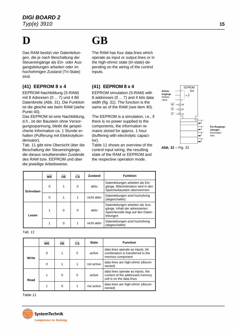
GB D Das RAM besitzt vier Datenleitun-gen, die je nach Beschaltung der Steuereingänge als Ein- oder Aus-gangsleitungen arbeiten oder im hochohmigen Zustand (Tri-State) sind.
(41) EEPROM 8 x 4 EEPROM-Nachbildung (S-RAM) mit 8 Adressen (0 ... 7) und 4 Bit Datenbreite (Abb. 31). Die Funktion ist die gleiche wie beim RAM (siehe Punkt 40). Das EEPROM ist eine Nachbildung, d.h., ist der Baustein ohne Versor-gungsspannung, bleibt die gespei-cherte Information ca. 1 Stunde er-halten (Pufferung mit Elektrolytkon-densator). Tab. 11 gibt eine Übersicht über die Beschaltung der Steuereingänge, die daraus resultierenden Zustände des RAM bzw. EEPROM und über die jeweilige Arbeitsweise.
Tab. 11
Table 11
WE––––
OE–––
CS–––
Zustand Funktion
0 1 0 aktiv Datenleitungen arbeiten als Ein-gänge, Bitkombination wird in den Speicherbaustein übernommen Schreiben
0 1 1 nicht aktiv Datenleitungen sind hochohmig (abgeschaltet)
1 0 0 aktiv
Datenleitungen arbeiten als Aus-gänge, Inhalt der adressierten Speicherzelle liegt auf den Daten-leitungen Lesen
1 0 1 nicht aktiv Datenleitungen sind hochohmig (abgeschaltet)
WE––––
OE–––
CS–––
State Function
0 1 0 active data lines operate as inputs, bit combination is transferred to the memory component Write
0 1 1 not active data lines are high-ohmic (discon-nected)
1 0 0 active data lines operate as inputs, the content of the addressed memory cell is on the data lines Read
1 0 1 not active data lines are high-ohmic (discon-nected)
The RAM has four data lines which operate as input or output lines or in the high-ohmic state (tri-state) de-pending on the wiring of the control inputs.
(41) EEPROM 8 x 4 EEPROM simulation (S-RAM) with 8 addresses (0 ... 7) and 4 bits data width (fig. 31). The function is the same as of the RAM (see item 40). The EEPROM is a simulation, i.e., if there is no power supplied to the components, the information re-mains stored for approx. 1 hour (buffering with electrolytic capaci-tor). Table 11 shows an overview of the control input wiring, the resulting state of the RAM or EEPROM and the respective operation mode.
Abb. 31 – Fig. 31

16 DIGI BOARD 2 Typ(e) 3910
GB D • Schreiben/Lesen:
− Betriebsspannung (+5V DC) anlegen
− Eingang CS über 2-mm-Verbindungsstecker an High-Pegel legen
− Eingänge WE und OE über Eingabetastatur beschalten
− Adresseingänge (0 ... 2) mit gewünschter Speicheradres-se(High-/Low-Pegel) beschal-ten
− Ein-/Ausgänge mit LEDs ver-binden
− Ausgangszustand: Am Eingang WE
––––– liegt Low-
Pegel und am Eingang OE––––
High-Pegel. An den Adress-eingängen liegt die gewünsch-te Speicheradresse.
− Abzuspeichernde Bitkombina-tion an Ein-/Ausgängen anle-gen
− Zum Speichern Eingang CS––––
kurz auf Low-Pegel legen.
− Angelegte Bitkombination von Ein-/Ausgängen entfernen (LEDs bleiben angeschlossen)
− Zum Auslesen Eingang WE–––––
an High-Pegel und Eingang OE––––
an Low-Pegel legen. Die gewünschte Speicheradresse an den Adresseingängen ein-stellen.
− Der Auslesevorgang erfolgt durch Anlegen eines Low-Pegels an den Eingängen CS
––––
in Abhängigkeit von der ge-wählten Speicheradresse.
• Write/read: − Apply operating voltage
(+5 V DC) − Apply input CS to high level by
a 2-mm connecting plug
− Wire inputs WE and OE with input keyboard
− Wire address inputs (0 ... 2) with desired memory address (high/low levels)
− Connect inputs/outputs to LEDs
− Output state: The input WE
–––––carries low level
and the input OE––––
high level. The address inputs carry the desired memory address.
− Apply bit combination to be stored to inputs/outputs
− For storing, apply input CS––––
to low level for a short time.
− Disconnect the applied bit combination from the in-puts/outputs (LEDs remain connected)
− For reading out apply input WE–––––
to high level and input OE––––
to low level. Adjust the desired memory address at the ad-dress inputs.
− For reading out apply a low level to the CS
–––– inputs depend-
ent on the selected memory address.

DIGI BOARD 2 Typ(e) 3910 17
GB D 5 Mechanische Daten Die Frontplatte des DIGI BOARD 2 besteht aus 5 mm starkem Schicht-pressstoff.
Die Rückseite ist zum Schutz mit einer grauen Kunststoffhaube ab-gedeckt, die durch ihre Formge-bung eine arbeitsgerechte Schräg-lage des Geräts, z.B. auf einem Tisch, ermöglicht.
DIGI BOARD 2 (Typ 3910):
Abmessungen: 532 x 297 x 95 mm (B x H x T)
Gewicht: ca. 3,5 kg
6 Empfohlenes Zubehör
• Zubehörsatz (Typ 3910.1)
• Handbuch: Versuche zur Digital-technik (Typ V 0160)
5 Mechanical Data The front panel of the DIGI BOARD 2 is made of 5 mm thick laminate.
The rear of the Board is protected with a grey plastic cover. Its shape allows the Board to be placed at an ergonomically favourable angle for example on a bench.
DIGI BOARD 2 (Type 3910):
Dimensions: 532 x 297 x 95 mm (w x h x d)
Weight: approx. 3.5 kg
6 Recommended Accessories
• Set of Accessories (Type 3910.1)
• Manual: Experiments in Digital Technology (Type V 0160)

18 DIGI BOARD 2 Typ(e) 3910
GB D 7 Erweiterungen Mit den nachfolgend aufgeführten Geräten und Bauelementen können zusätzlich Versuche durchgeführt werden, die im Handbuch „Versu-che zur Digitaltechnik“ nicht aufge-führt sind.
• UNIVERSAL BOARD 1 (Typ 8175)
• UNIVERSAL BOARD 2 (Typ 8176)
• Universal-Aufbauplatte (Typ 1012.1)
• Universal-Aufbauplatte (Typ 1012.2)
• Module zur Digitaltechnik (Serie 9400)
• IC BOARD (Typ 3530)
• IC-Fassung (dual-in-line) (Typ 9156)
• IC-Fassung, 20polig (Typ 9156.2)
• IC-Fassung, 28polig (Typ 9156.3)
• Bausatz bestehend aus:
− Leergehäuse (Typ 9152.7) − Experimentierplatine mit
Punktraster (Typ 9167) − Experimentierplatine mit
Streifenraster (Typ 9167.1) − Bundhülsen (Typ 9168) − Schild (Typ 9162.5-6)
7 Expansions Additional experiments not de-scribed in the manual „Experiments in Digital Technology“ can be con-ducted with the equipments and components listed below.
• UNIVERSAL BOARD 1 (Type 8175)
• UNIVERSAL BOARD 2 (Type 8176)
• Universal Assembly Board (Type 1012.1)
• Universal Assembly Board (Type 1012.2)
• Modules for digital technology (Series 9400)
• IC BOARD (Type 3530)
• IC Socket, dual-in-line (Type 9156)
• IC Socket, 20-pin (Type 9156.2)
• IC Socket, 28-pin (Type 9156.3)
• Assembly kit consisting of:
− Empty Housing (Type 9152.7)− Experiment Board with Dot
Grid (Type 9167), − Experiment Board with Line
Grid (Type 9167.1) − Jacks (Type 9168) − Sticker (Type 9162.5-6)

Sicherheitshinweise 0.
6.2
Sicherheitshinweise zu hps Lehr- und Lernsystemen Lehr- und Lernsysteme von hps SystemTechnik werden nach den anerkannten Regeln der Technik gebaut und geprüft. Bei bestimmungsgemäßer Verwendung ist die Sicherheit von Anwender und Gerät gewährleistet.
Da beim Experimentieren mit elektrischer Energie in Unterrichtsräumen dennoch Gefahren auftreten können, ist es notwendig, folgende Sicherheitshinweise zu beachten:
• Die Unfallverhütungsvorschriften für elektrische Anlagen und Betriebsmittel sowie für nicht elektrische Arbeiten in der Nähe elektrischer Anlagen und Betriebsmittel sind einzuhalten.
• Die bestimmungsgemäße Verwendung ist durch folgende Punkte fest definiert:
- Das Lehr- und Lernsystem darf nur zu schulischen und ausbildungstechnischen Unterweisungen verwendet werden.
- Der Einsatzort ist auf schulische und ausbildungstechnische Räume begrenzt.
• Geräte, an denen eine Fehlfunktion festgestellt worden ist, dürfen dem Anwender nicht mehr zu-gänglich gemacht werden.
- Anwender müssen in angemessenen Zeitabständen über mögliche Gefahren unterrichtet werden.
• Sicherheitshinweise in der Gerätebeschreibung, dem Handbuch oder auf den Lehr- und Lernsystemen müssen eingehalten und vor Inbetriebnahme nachgelesen werden:
Achtung, lebensgefährliche Berührungsspannungen!
Achtung, Gerätebeschreibung, Systembeschreibung oder Handbuch beachten!
• Reparaturen an Lehr- bzw. Lernsystemen dürfen nur von Elektrofachkräften durchgeführt werden!
• Nach der Reparatur sind bei Geräten, die berührungsgefährliche Spannungen führen, folgende Punkte unbedingt zu prüfen:
- Richtiger Schutzleiteranschluss, wenn vorhanden - Isolationsprüfung bei Geräten ohne Schutzleiteranschluss - Funktionsprüfung des Geräts
hps SystemTechnik Tel.: 07 51 / 5 60 75 70 Lehr- + Lernmittel GmbH Fax: 07 51 / 5 60 75 77 Altdorfer Straße 16 Web: www.hps-systemtechnik.com 88276 Berg E-Mail: [email protected]

Safety Instructions 0.
6.2
Safety Instructions for hps Teaching and Learning Systems Teaching and learning systems from hps SystemTechnik are built and tested according to the recog-nized technical rules. The security of user and devices are assured when using the devices in accor-dance with the regulations.
Nevertheless dangers may appear when making experiments using electrical energy in class rooms. It is therefore necessary to observe the following safety instructions:
• The regulations for prevention of accidents regarding electric installations and devices, as well as non-electrical works carried out near electric installations and devices are to be observed.
• The use in accordance with the regulations is defined as follows:
- The teaching and learning system may only be used for instructions at school or for training. - The site where it may be used is restricted to class rooms or rooms for technical training.
• Devices of defective performance may no longer be made accessible to the user.
- Users are to be informed of possible dangers in reasonable time intervals.
• Safety instructions, given in the technical description, the manual or on the teaching and learning systems themselves are to be observed and remembered before starting operation:
Warning, dangerous shock-hazard voltages!
Warning, observe technical description, system description or manual!
• Repairs of teaching and learning systems may only be carried out by electrical specialists!
• With devices carrying voltages implying a risk of electric shock, following has to be checked after repair:
- Correct connection of protective conductors, if existing - Insulation check on devices without protective conductor connection - Performance check of the device
hps SystemTechnik Phone: + 49 751 / 5 60 75 80 Lehr- + Lernmittel GmbH Fax: + 49 751 / 5 60 75 17 Altdorfer Strasse 16 Web: www.hps-systemtechnik.com 88276 Berg (Germany) E-Mail: [email protected]