
CUDA를 활용한 실시간IMAGE PROCESSING
SYSTEM 구현
Chang Hee Lee
1

Overview
Thin film transistor(TFT) LCD : Inspection Object Type of DefectType of Inspection
Instrument BriefLighting / FocusingOptic MagnificationScanning
Electrical System ComponentSensor / CameraGrabber
ProcessingInspection Spec.Speed ObstacleAlgorithm / Implementation with CUDA
2

Schematic of TFT
3

Types of TFTs
TN + film (Twisted nematic)IPS (LG-Philips , Hitachi, 1996)
IPS (in-plane switching)AS-IPS (Advanced Super-IPS) – LG-PhilipsA-TW-IPS (Advance True White-IPS) – LG-Philips
VA (Samsung, Fujitsu, 1998)MVA (multi-domain vertical alignment)PVA (patterned vertical alignment) - Samsung
4

TN
5
Low Driving VoltageNarrow viewing angle

IPS
6
Very wide viewing angle
Slow Response speedLow brightness

VA
7
High Contrast Ratio
Wide viewing AngleFast Response speed
Figure: Koike, Y, Super high quality MVA-TFT liquid crystal displays 1999

Types of Defects (Color Filter) (1/2)
Macro-Defects (can be find by human eyes)IRO-MURA : Unevenness of colorSIMI : Stain on a filterIRO-ZURE : mis-alignmeant of color cells
8 Reference : K-NAKASHIMA, Hybrid Inspection System for LCD Color Filter Panels 1994
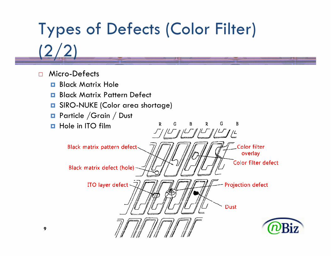
Types of Defects (Color Filter) (2/2)
9
Micro-DefectsBlack Matrix HoleBlack Matrix Pattern DefectSIRO-NUKE (Color area shortage)Particle /Grain / DustHole in ITO film
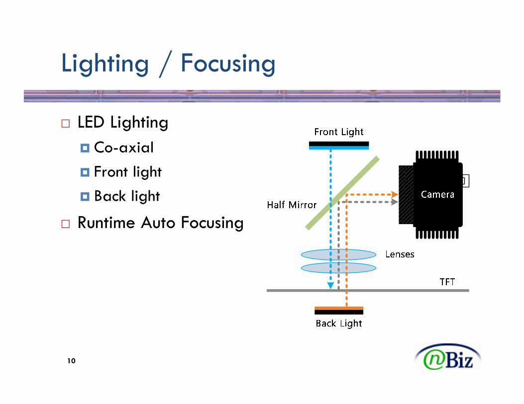
Lighting / Focusing
LED LightingCo-axialFront lightBack light
Runtime Auto Focusing
10

Optical Magnification
2x, 10x magnification
11

Scanning
12

Array & Scanning
Unidirectional WayBidirectional WayRepetition (Multi Line Scan)
Related to magnificationLarge No. of Repetition Increase No. of Camera7 Gen. 2x, 10 Camera (7μm) : 8 times
13

Electrical System Components
Sensor / Camera2K TDI Camera (13μm x 13μm, Max. 52KHz, 104MByte/s)8K Linear Sensor (7μm x 7μm, Max. 33KHz, 264MByte/s)8K TDI Camera (7μm x 7μm, Max. 68KHz, 640MByte/s)
Grabber : Matrox’s Solios eCL/XCLCPU : Intel’s Dual Core, 2.4GHzGPU : nVidia’s FX5600OS : Window XP ProfessionalSoft Development Environment : MS Visual Studio 2005
14
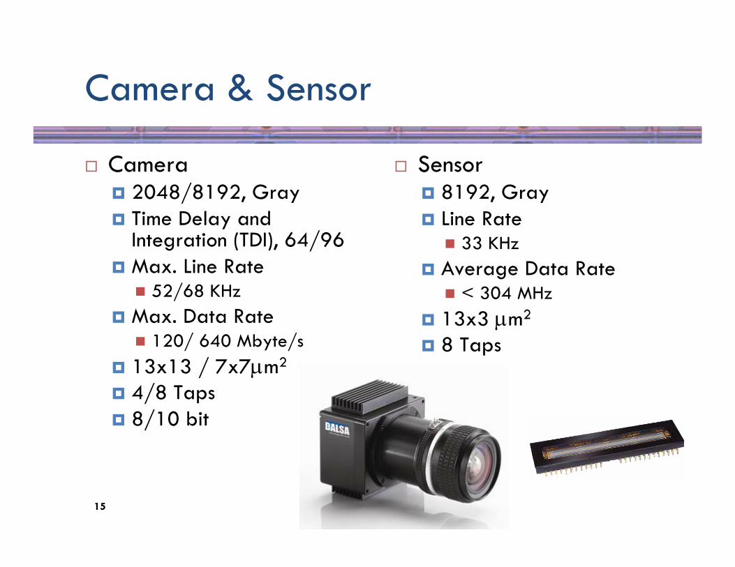
Camera & Sensor
Camera2048/8192, GrayTime Delay and Integration (TDI), 64/96Max. Line Rate
52/68 KHzMax. Data Rate
120/ 640 Mbyte/s13x13 / 7x7μm2
4/8 Taps8/10 bit
Sensor8192, GrayLine Rate
33 KHzAverage Data Rate
< 304 MHz13x3 μm2
8 Taps
15

Grabber
Matrox’s Solios eCL/XCLSmall amount of Preprocessing
x4 PCI express/ PCI-XPCI express : 1GByte/s for each directionPCI-X (64bit, 133MHz) : 1GByte/s
64 MB acquisition bufferRelatively Small buffer size - It’s enoughFrame(number of line) Options
2K x 500/1000/2000/4000 line1/2/4/8 MB per frame
Camera LinkDual Base/Medium LinkFull Link
16

Micro Inspection Specification
Camera/Sensor : Area/LineEnlarge Defect Area after Macro InspectionRepair defectsResolution
Below 1μm x 1μm (About x10 optically magnified)Total Amount of Data
Proportion to no. of Areas where defects possibly existRequired Processing Power
Looser but Real Time (large amount of data)Up to Camera maximum speed120 Mbyte/s
17

Macro Inspection Specification
18
Scan Entire Area7th Generation TFT
Size : 2200 x 2520mmResolution : about 5μm x 5μmTotal Amount of Data : 221.8GB per Panel

Data Rate
19
No. of CamerasInspection Time / Processing SpeedResolutionCurrent Primary Target
~640MByte/s

Speed Obstacles
20
Image Quality (Simplifying Algorithm)Unstabilized Focus Scan speed perturbationUnevenness of LightLens distortion
Reduce Camera Cell dimension / Enlarge lens diameterOrientationLarge no. of defectsSensor/Electrical Noise
Algorithm ProcessingSensor/Camera Acquisition SpeedData Transfer BandwidthProcessing Speed
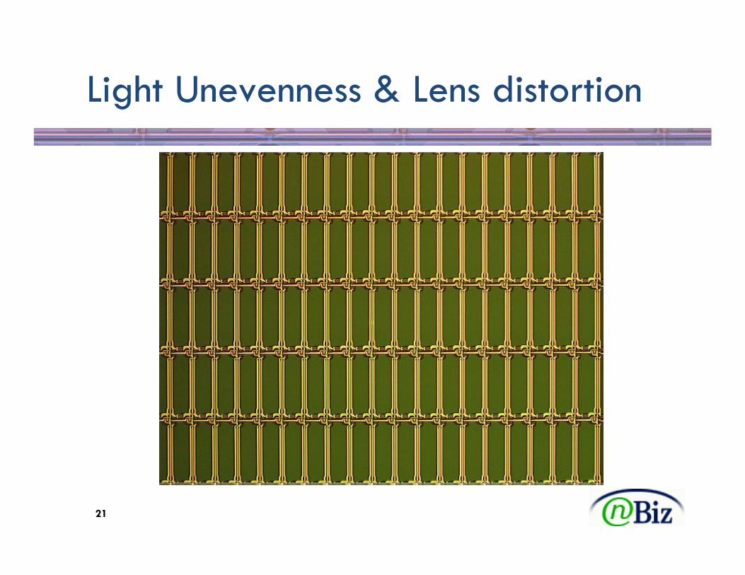
Light Unevenness & Lens distortion
21

Scan Speed Perturbation
22
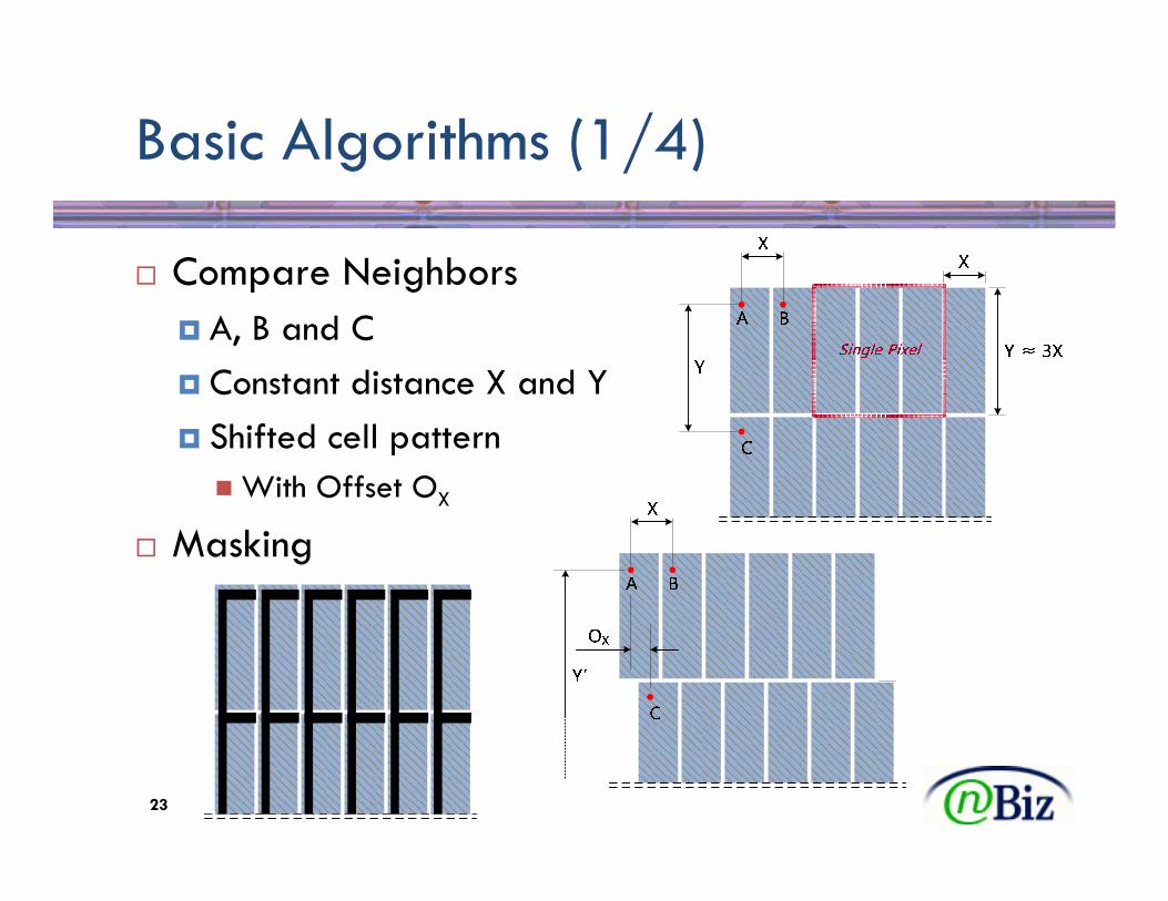
Basic Algorithms (1/4)
Compare NeighborsA, B and CConstant distance X and YShifted cell pattern
With Offset OX
Masking
23

Basic Algorithm (2/4)
24
1D FFT (Macro Inspection)
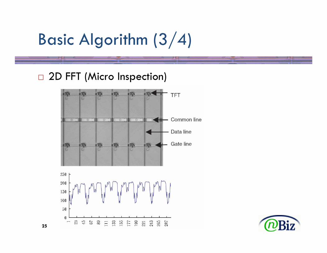
Basic Algorithm (3/4)
25
2D FFT (Micro Inspection)

Basic Algorithm (4/4)
26
Results
Reference : D.-M. TSAI, One-dimensional-based automatic defect inspection of multiple patterned TFT-LCD panels using Fourier image reconstruction 2007
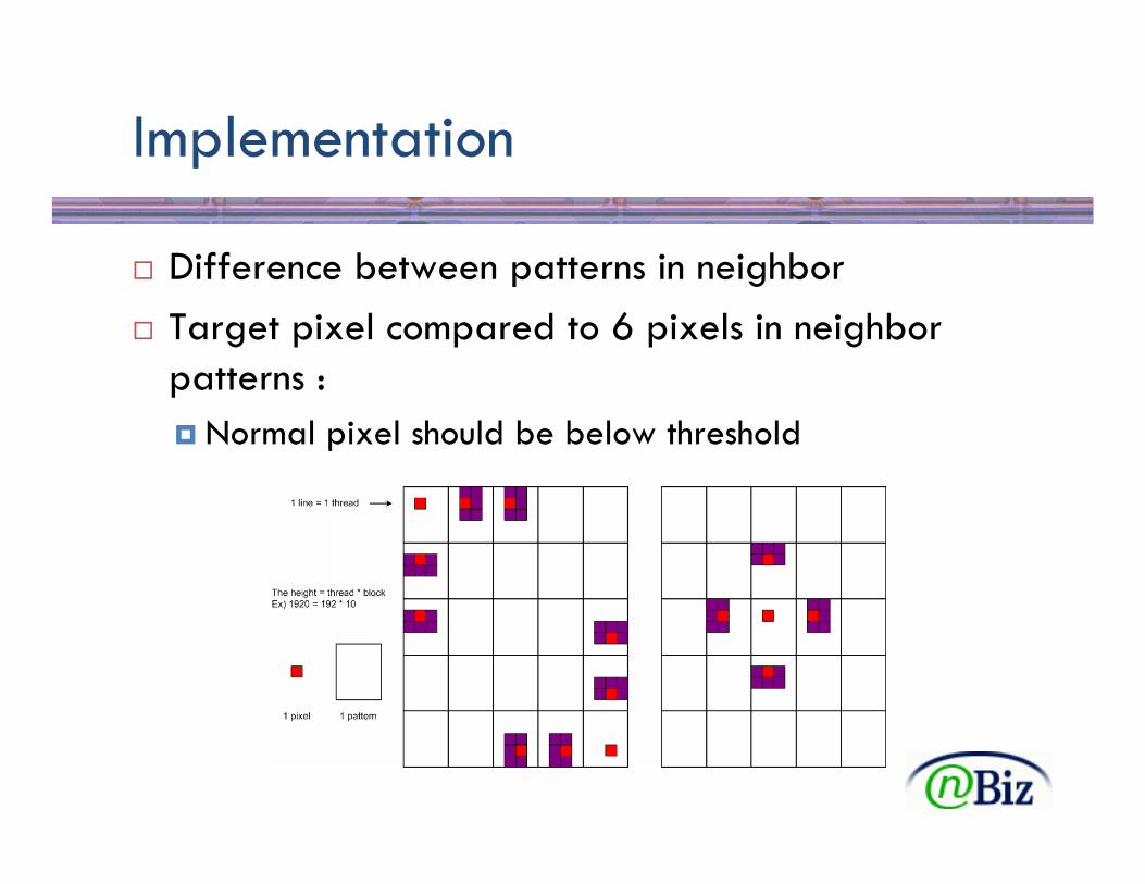
Implementation
Difference between patterns in neighborTarget pixel compared to 6 pixels in neighbor patterns :
Normal pixel should be below threshold

Implementation on GPU
1 thread process through single line One Dimensional block/thread
32 blocks in grid, 64 threads in a block (2048 thread)Optimal : 32 threads in a warpNo. of threads can be increased by 32 times from 96 to 384
Process from left to right

8MByte Processing Time (1/2)
29
2048x500 (≈1MByte) : Transfer ratio : 78 %2048x1000 (≈2MByte) : Transfer ratio : 72 %2048x2000 (≈4MByte) : Transfer ratio : 69 %
Best GPU efficiency2048x4000 (≈8MByte) : Transfer ratio : 67 %
Best Transfer efficiency

Processing Time (2/2)
30
Reduce Data Transfer TimeEnlarge frame sizeReduce Result DataUse streamingIncrease data Bandwidth (Host GPU)

Required Bandwidth (1/2)
Target Sensor/Camera Data Rate : 640MByte/s
Extra CPU Main Memory (DDR2) Access
IO (Hard disk), DRAM Refresh / PhasingKernel/Application/GraphicDMA Management
31

Required Bandwidth (2/2)
Actual ValueHost to Device (vice versa): 1.6 GByte/sDevice to Device : 62 GByte/s
32

Embedded System
33
Reduce No. of ComputersSolve the bandwidth problem

Conclusion
TFT Inspection SystemTypical case of Single Instruction, Multiple Data (SIMD)
Relatively simple instruction/algorithmHuge amount of data – Data Bandwidth important
Currently 120MByte/s is achieved with CUDA640Mbyte/s will be possible achieved with CUDA
Increase Data BandwidthEmbedded systemReduce extra transfer / Optimize Algorithm
34

Thank You !
35


