ACCESS IC LAB
Graduate Institute of Electronics Engineering, NTU
Fundamentals of Hardware Description Language
Lecturer: Yu-Hao Chen(陳郁豪)Date: 2011.03.02
Based on: Ch.1-3 of the textbookReview: Logic Design (Concepts of Propagation Delay)
Graduate Institute of Electronics Engineering, NTU
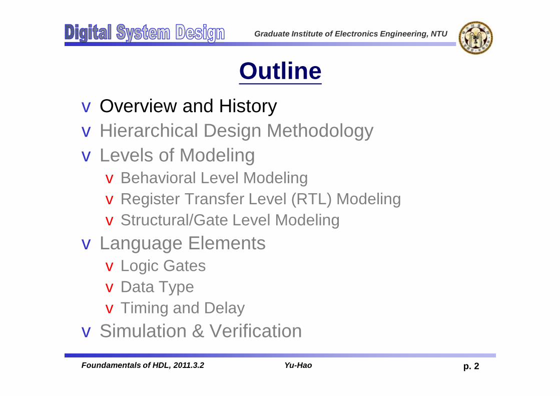
OutlinevOverview and HistoryvHierarchical Design MethodologyvLevels of ModelingvBehavioral Level ModelingvRegister Transfer Level (RTL) Modeling vStructural/Gate Level Modeling
vLanguage ElementsvLogic GatesvData TypevTiming and Delay
vSimulation & Verification
p. 2Foundamentals of HDL, 2011.3.2 Yu-Hao

Graduate Institute of Electronics Engineering, NTU
v Hardware Description Language (HDL) is any language from a class of computer languages and/or programming languages for formal description of electronic circuits, and more specifically, digital logic.
v HDL canv describe the circuit's operation, design, organizationv verify its operation by means of simulation.
v Now HDLs usually merge Hardware Verification Language, which is used to verify the described circuits.
From Wikipedia
p. 3Foundamentals of HDL, 2011.3.2 Yu-Hao
Hardware Description Language (1/2)

Graduate Institute of Electronics Engineering, NTU
v HDLs are used to write executable specifications of some piece of hardware. v Designed to implement the semantics of the language
statements with native supporting to simulate the progress of time
v Being executablev Provides the hardware designer the ability to model a piece
of hardware before it is created physically.
v Supporting discrete-event (digital) or continuous-time (analog) modeling, e.g.:v SPICE, Verilog HDL, VHDL, SystemC
p. 4Foundamentals of HDL, 2011.3.2 Yu-Hao
Hardware Description Language (2/2)

Graduate Institute of Electronics Engineering, NTU
High-Level Programming Languagev It’s possible to describe a hardware (operation,
structure, timing, and testing methods) in C/C++/Java, why do we use HDL?
v The efficiency (to model/verify) does matter.
v Native support to concurrencyv Native support to the simulation of the progress of timev Native support to different model of signal states
v The required level of detail determines the language we use.
p. 5Foundamentals of HDL, 2011.3.2 Yu-Hao

Graduate Institute of Electronics Engineering, NTU
List of HDL for Digital Circuits
v Verilogv VHDLv Advanced Boolean Expression Language (ABEL)v AHDL (Altera HDL, a proprietary language from Altera)v Atom (behavioral synthesis and high-level HDL based on Haskell)v Bluespec (high-level HDL originally based on Haskell, now with a
SystemVerilog syntax)v Confluence (a functional HDL; has been discontinued)v CUPL (a proprietary language from Logical Devices, Inc.)v Handel-C (a C-like design language)v C-to-Verilog (Converts C to Verilog)v HDCaml (based on Objective Caml)v Hardware Join Java (based on Join Java)v HML (based on SML)v Hydra (based on Haskell)v Impulse C (another C-like language)v JHDL (based on Java)Lava (based on Haskell)v Lola (a simple language used for teaching)v MyHDL (based on Python)
v PALASM (for Programmable Array Logic (PAL) devices)
v Ruby (hardware description language)v RHDL (based on the Ruby programming
language) SDL based on Tcl.v CoWareC, a C-based HDL by CoWare. Now
discontinued in favor of SystemC
v SystemVerilog, a superset of Verilog, with enhancements to address system-level design and verification
v SystemC, a standardized class of C++ libraries for high-level behavioral and transaction modeling of digital hardware at a high level of abstraction, i.e. system-level
v SystemTCL, SDL based on Tcl.
p. 6Foundamentals of HDL, 2011.3.2 Yu-Hao

Graduate Institute of Electronics Engineering, NTU
About Verilogv Introduction on 1984 by Phillip Moorby and Prabhu
Goel in Automated Integrated Design System (renamed to Gateway Design Automation and bought by Cadence Design Systems)
v Open and Standardize (IEEE 1364-1995) on 1995 by Cadence because of the increasing success of VHDL (standard in 1987)
v Become popular and makes tremendous improvement on productivityv Syntax similar to C programming language, though the
design philosophy differs greatly
p. 7Foundamentals of HDL, 2011.3.2 Yu-Hao

Graduate Institute of Electronics Engineering, NTU
History/Branch of Verilog
VerilogIEEE Std 1364-1995
Verilog-2001IEEE Std 1364-2001
Verilog-2005IEEE Std 1364-2005
SystemVerilogIEEE Std 1800-2005
Digital-signal HDL
p. 8Foundamentals of HDL, 2011.3.2 Yu-Hao

Graduate Institute of Electronics Engineering, NTU
OutlinevOverview and HistoryvHierarchical Design MethodologyvLevels of ModelingvBehavioral Level ModelingvRegister Transfer Level (RTL) Modeling vStructural/Gate Level Modeling
vLanguage ElementsvLogic GatesvData TypevTiming and Delay
vSimulation & Verification
p. 9Foundamentals of HDL, 2011.3.2 Yu-Hao
Graduate Institute of Electronics Engineering, NTU
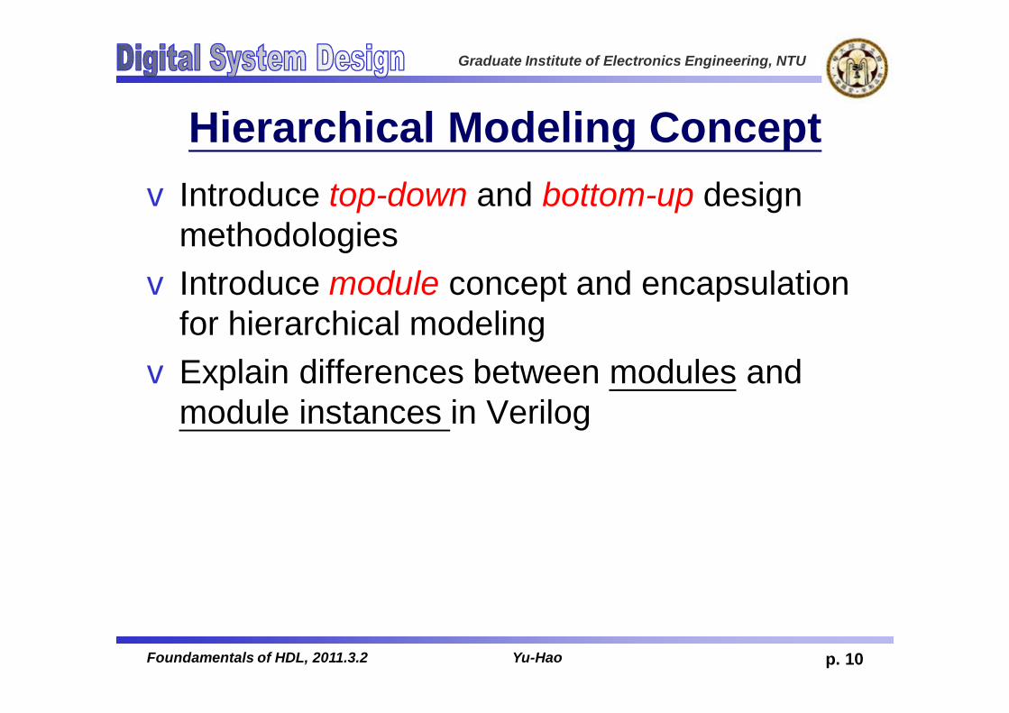
Hierarchical Modeling ConceptvIntroduce top-down and bottom-up design
methodologiesvIntroduce module concept and encapsulation
for hierarchical modelingvExplain differences between modules and
module instances in Verilog
p. 10Foundamentals of HDL, 2011.3.2 Yu-Hao

Graduate Institute of Electronics Engineering, NTU
Top-down Design Methodologyv We define the top-level block and identify the sub-blocks
necessary to build the top-level block.v We further subdivide the sub-blocks until we come to leaf cells,
which are the cells that cannot further be divided.
Top levelblock
subblock 2
subblock 3
subblock 4
subblock 1
leafcell
leafcell
leafcell
leafcell
leafcell
leafcell
leafcell
leafcell
p. 11Foundamentals of HDL, 2011.3.2 Yu-Hao

Graduate Institute of Electronics Engineering, NTU
Bottom-up Design Methodologyv We first identify the building block that are available to us.v We build bigger cells, using these building blocks.v These cells are then used for higher-level blocks until we build
the top-level block in the design.
Top levelblock
macrocell 2
macrocell 3
macrocell 4
macrocell 1
leafcell
leafcell
leafcell
leafcell
leafcell
leafcell
leafcell
leafcell
p. 12Foundamentals of HDL, 2011.3.2 Yu-Hao
Graduate Institute of Electronics Engineering, NTU
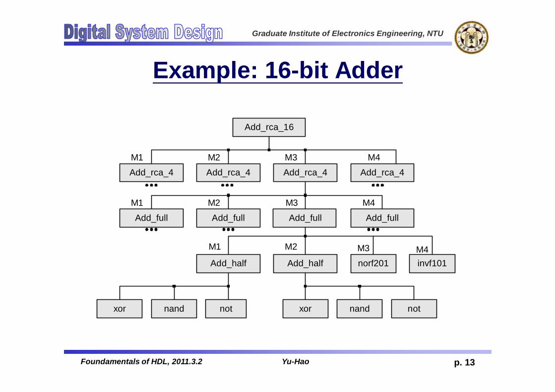
Example: 16-bit Adder
Add_full
Add_half norf201 invf101
M1 M2
xor nand notnotnandxor
M3 M4
Add_rca_16
Add_rca_4Add_rca_4Add_rca_4 Add_rca_4
M1
Add_fullAdd_fullAdd_full
M2 M3 M4
M1 M2 M3 M4
Add_half
p. 13Foundamentals of HDL, 2011.3.2 Yu-Hao

Graduate Institute of Electronics Engineering, NTU
Hierarchical Modeling in Verilogv A Verilog design consists of a hierarchy of modules.
vModules encapsulate design hierarchy, and communicate with other modules through a set of declared input, output, and bidirectional ports.
v Internally, a module can contain any combination of the followingv net/variable declarations (wire, reg, integer, etc.)v concurrent and sequential statement blocksv instances of other modules (sub-hierarchies).
p. 14Foundamentals of HDL, 2011.3.2 Yu-Hao

Graduate Institute of Electronics Engineering, NTU
Design Encapsulationv Encapsulate structural and functional details in a
module
v Encapsulation makes the model available for instantiation in other modules
module <Module Name> (<PortName List>);
// Structural part<List of Ports><Lists of Nets and Registers><SubModule List> <SubModule Connections>
// Behavior part<Timing Control Statements>
<Parameter/Value Assignments><Stimuli><System Task>
endmodule
p. 15Foundamentals of HDL, 2011.3.2 Yu-Hao
Graduate Institute of Electronics Engineering, NTU
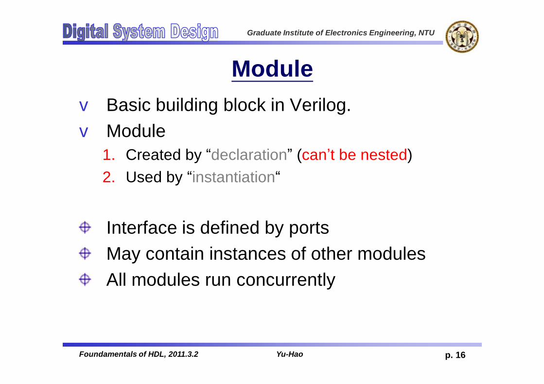
Module v Basic building block in Verilog.v Module
1. Created by “declaration” (can’t be nested)2. Used by “instantiation“
Interface is defined by portsMay contain instances of other modulesAll modules run concurrently
p. 16Foundamentals of HDL, 2011.3.2 Yu-Hao

Graduate Institute of Electronics Engineering, NTU
Instancesv A module provides a template from which you can
create actual objects.vWhen a module is invoked, Verilog creates a unique
object from the template.v Each object has its own name, variables, parameters
and I/O interface.
p. 17Foundamentals of HDL, 2011.3.2 Yu-Hao

Graduate Institute of Electronics Engineering, NTU
Module Instantiation
Adder
Adder Adder
Adder_tree
instance example
p. 18Foundamentals of HDL, 2011.3.2 Yu-Hao

Graduate Institute of Electronics Engineering, NTU
Analogy: module ↔ class
Syntax module m_Name( IO list );...endmodule
class c_Name {...};
Instantiation m_Name ins_name ( port connection list );
c_Name obj_name;
Member ins_name.member_signal obj_name.member_data
Hierachy instance.sub_instance.member_signal
object.sub_object.member_data
As module is to Verilog HDL, so class is to C++programming language.
p. 19Foundamentals of HDL, 2011.3.2 Yu-Hao

Graduate Institute of Electronics Engineering, NTU
Analogy: module ↔ class
vassign and evaluate() is simulated/called at each Ti+1 = Ti + tresolution
Model AND gate with C++ Model AND gate with Verilog HDL
p. 20Foundamentals of HDL, 2011.3.2 Yu-Hao

Graduate Institute of Electronics Engineering, NTU
OutlinevOverview and HistoryvHierarchical Design MethodologyvLevels of ModelingvBehavioral Level ModelingvRegister Transfer Level (RTL) Modeling vStructural/Gate Level Modeling
vLanguage ElementsvLogic GatesvData TypevTiming and Delay
vSimulation & Verification
p. 21Foundamentals of HDL, 2011.3.2 Yu-Hao

Graduate Institute of Electronics Engineering, NTU
Cell-Based Design and Levels of Modeling
p. 22Yu-HaoFoundamentals of HDL, 2011.3.2
Behavioral Level
Register Transfer Level (RTL)
Structural/Gate Level
Transistor/Physical Level
Most used modeling level, easy for designer, can be simulated and synthesized to gate-level by EDA toolsCommon used modeling level for small sub-modules, can be simulated and synthesized to gate-level
Usually generated by synthesis tool by using a front-end cell library, can be simulated by EDA tools. A gate is mapped to a cell in library
Usually generated by synthesis tool by using a back-end cell library, can be simulated by SPICE

Graduate Institute of Electronics Engineering, NTU
Tradeoffs Among Modeling Levelsv Each level of modeling permits modeling at a higher or
lower level of detail. More detail means more efforts for designers and the simulator.
v Always keep in mind which level of modeling is adopted
p. 23Foundamentals of HDL, 2011.3.2 Yu-Hao

Graduate Institute of Electronics Engineering, NTU
An Example1-bit Multiplexer
in1
in2out
0
1
sel
if (sel==0) out = in1;else out = in2;
sel in1 in2 out
0 0 0 0
0 0 1 0
0 1 0 1
0 1 1 1
1 0 0 0
1 0 1 1
1 1 0 0
1 1 1 1
p. 24Foundamentals of HDL, 2011.3.2 Yu-Hao
To “select” output
out = (sel’ & in1) + (sel & in2)

Graduate Institute of Electronics Engineering, NTU
Gate Level Description
a1
a2
in1
in2
sel
outo1
iv_sel a1_o
a2_on1
iv_sel
Gate Level: you see only netlist (gates and wires) in the code
p. 25Foundamentals of HDL, 2011.3.2 Yu-Hao

Graduate Institute of Electronics Engineering, NTU
Behavioral Level/RTL Description
RTL: describe logic/arithmetic function between input node and output node
Behavior: RTL in an event-driven behavior description construct
always block assign
p. 26Foundamentals of HDL, 2011.3.2 Yu-Hao

Graduate Institute of Electronics Engineering, NTU
OutlinevOverview and HistoryvHierarchical Design MethodologyvLevels of ModelingvBehavioral Level ModelingvRegister Transfer Level (RTL) Modeling vStructural/Gate Level Modeling
vLanguage ElementsvLogic GatesvData TypevTiming and Delay
vSimulation & Verification
p. 27Foundamentals of HDL, 2011.3.2 Yu-Hao
Graduate Institute of Electronics Engineering, NTU
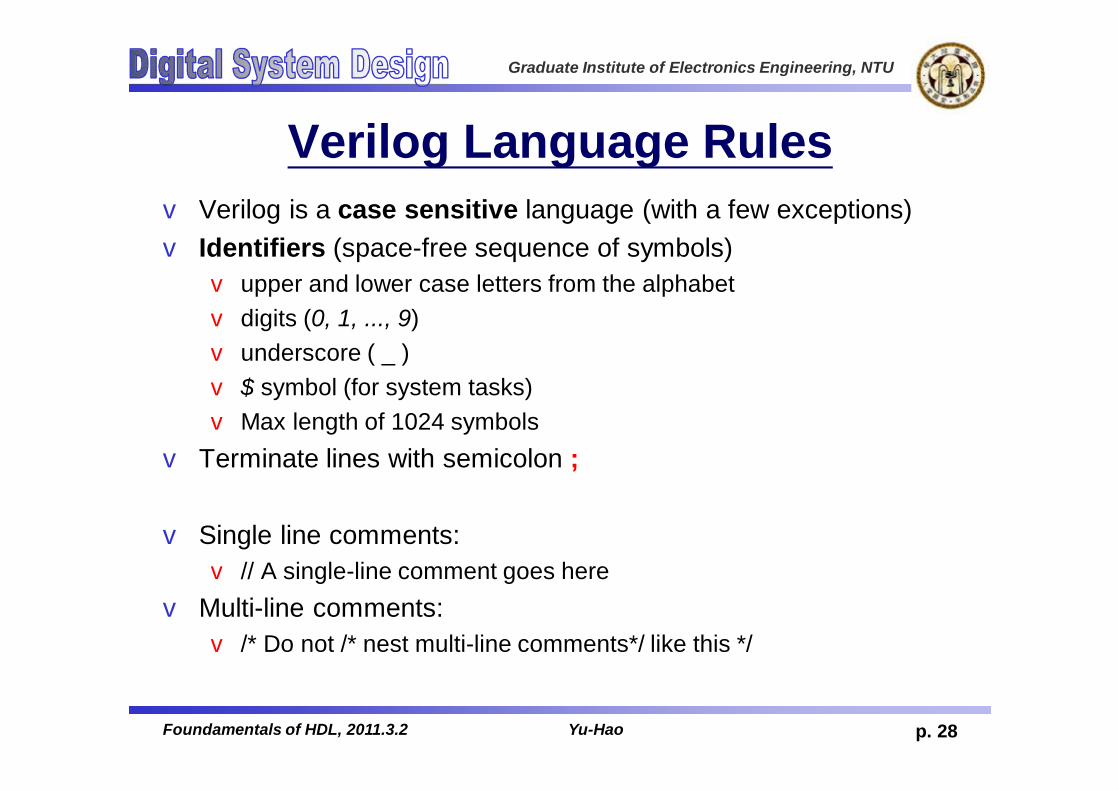
Verilog Language Rulesv Verilog is a case sensitive language (with a few exceptions)v Identifiers (space-free sequence of symbols)v upper and lower case letters from the alphabetv digits (0, 1, ..., 9)v underscore ( _ )v $ symbol (for system tasks)v Max length of 1024 symbols
v Terminate lines with semicolon ;
v Single line comments:v // A single-line comment goes here
v Multi-line comments:v /* Do not /* nest multi-line comments*/ like this */
p. 28Foundamentals of HDL, 2011.3.2 Yu-Hao

Graduate Institute of Electronics Engineering, NTU
Verilog Basis CellvVerilog Basis Componentsvparameter declarationsvnets or reg declarationsvport declarationsvContinuous assignmentsvModule instantiationsvGate instantiationsvFunction definitionsvalways blocksvtask statements
p. 29Foundamentals of HDL, 2011.3.2 Yu-Hao
Graduate Institute of Electronics Engineering, NTU
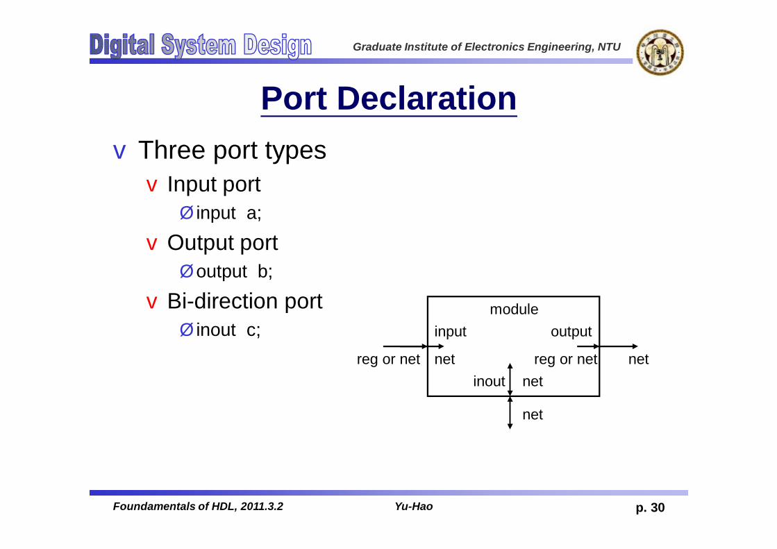
Port DeclarationvThree port typesvInput portØ input a;
vOutput portØoutput b;
vBi-direction portØ inout c;
net
net
netnet
input output
inoutreg or net reg or net
module
p. 30Foundamentals of HDL, 2011.3.2 Yu-Hao
Graduate Institute of Electronics Engineering, NTU
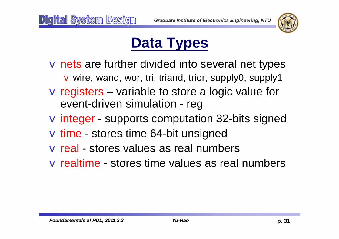
Data Typesvnets are further divided into several net typesvwire, wand, wor, tri, triand, trior, supply0, supply1
vregisters – variable to store a logic value for event-driven simulation - regv integer - supports computation 32-bits signedvtime - stores time 64-bit unsignedvreal - stores values as real numbersvrealtime - stores time values as real numbers
p. 31Foundamentals of HDL, 2011.3.2 Yu-Hao

Graduate Institute of Electronics Engineering, NTU
Net Typesv The most common and important net typesv wire and triØ for standard interconnection wires
v supply 1 and supply 0
v Other wire typesv wand, wor, triand, and triorØ for multiple drivers that are wired-anded and wired-ored
v tri0 and tri1Ø pull down and pull up
v triregØ for net with capacitive storageØ If all drivers at z, previous value is retained
p. 32Foundamentals of HDL, 2011.3.2 Yu-Hao

Graduate Institute of Electronics Engineering, NTU
Register Typesv regv any size, unsigned
v integer (not synthesizable)v integet a,b; // declarationv 32-bit signed (2’s complement)
v time (not synthesizable)v 64-bit unsigned, behaves like a 64-bit regv $display(“At %t, value=%d”,$time,val_now)
v real, realtime (not synthesizable)v real c,d; //declarationv 64-bit real numberv Defaults to an initial value of 0
p. 33Foundamentals of HDL, 2011.3.2 Yu-Hao

Graduate Institute of Electronics Engineering, NTU
Integer, Real, & Time
vData types not for hardware descriptionvFor simulation control, data, timing extraction.
v integer counter;vinitial counter = -1;
vreal delta;vinitial delta = 4e10;
vtime sim_time;vinitial sim_time = $time;
p. 34Foundamentals of HDL, 2011.3.2 Yu-Hao

Graduate Institute of Electronics Engineering, NTU
Wire & Regv wire(wand, wor, tri)v Physical wires in a circuitv Cannot assign a value to a wire within a function or a
begin…..end block
v A wire does not store its value, it must be driven byØ by connecting the wire to the output of a gate or moduleØ by assigning a value to the wire in a continuous assignment
v An un-driven wire defaults to a value of Z (high impedance).v Input, output, inout port declaration -- wire data type
(default)
p. 35Foundamentals of HDL, 2011.3.2 Yu-Hao

Graduate Institute of Electronics Engineering, NTU
Wire & Regv regv A event driven variable in Verilog
v Use of “reg” data type is not exactly stands for a really DFF.
v Use of wire & regvWhen use “wire” è usually use “assign” and “assign” does
not appear in “always” blockvWhen use “reg” è only use “a=b” , always appear in “always”
blockmodule test(a,b,c,d);input a,b;output c,d;reg d;assign c=a;always @(b)
d=b;endmodule
p. 36Foundamentals of HDL, 2011.3.2 Yu-Hao

Graduate Institute of Electronics Engineering, NTU
Nets-Wired Logicv The family of nets includes the types wand and worv A wand net type resolves multiple driver as wired-and logic,
e.g. open collector technologyv A wor net type resolves multiple drivers as wired-or logic,
e.g. emitter-coupled technology
v The family of nets includes supply0 and supply1v supply0 has a fixed logic value of 0 to model a ground
connection v supply1 has a fixed logic value of 1 to model a power
connection
vUsed when model at transistor-level
p. 37Foundamentals of HDL, 2011.3.2 Yu-Hao

Graduate Institute of Electronics Engineering, NTU
More about Nets: Trivtri: a data type identified distinctively to
indicate that it will be thi-state (Z) in hardware, same functionality as wirevtriand and trior: similar as wand and worvtri0: resistive pull-downvtri1: resistive pull-upvtrireg: a net models the charge stored on a
physical net
vUsed when model at transistor-levelp. 38Foundamentals of HDL, 2011.3.2 Yu-Hao

Graduate Institute of Electronics Engineering, NTU
Data Type - Examplesreg a; // scalar registerwand b; // scalar net of type “wand”reg [3:0] c; // 4-bit registertri [7:0] bus; // tri-state 8-bit busreg [1:4] d; // 4-bittrireg (small) store; // specify logical strength (rare used)
a
b
c
0 1 X Z
0 0 X X 0
1 X 1 X 1
X X X X X
Z 0 1 X Z
0 1 X Z
0 0 0 0 0
1 0 1 X 1
X 0 X X X
Z 0 1 X Z
0 1 X Z
0 0 1 X 0
1 1 1 1 1
X X 1 X X
Z 0 1 X Z
wire/tri truth table wand/triand wor/trior
p. 39Foundamentals of HDL, 2011.3.2 Yu-Hao

Graduate Institute of Electronics Engineering, NTU
Vectorv wire and reg can be defined vector, default is 1bitv vector is multi-bits elementv Format: [High#:Low#] or [Low#:High#]v Using range specify part signals
wire a; // scalar net variable, defaultwire [7:0] bus; // 8-bit busreg clock; // scalar register, defaultreg [0:23] addr; // Vector register, virtual address 24 bits wide
bus[7] // bit #7 of vector busbus[2:0] // Three least significant bits of vector bus
// using bus[0:2] is illegal because the significant bit should// always be on the left of a range specification
addr[0:1] // Two most significant bits of vector addr
p. 40Foundamentals of HDL, 2011.3.2 Yu-Hao
Graduate Institute of Electronics Engineering, NTU
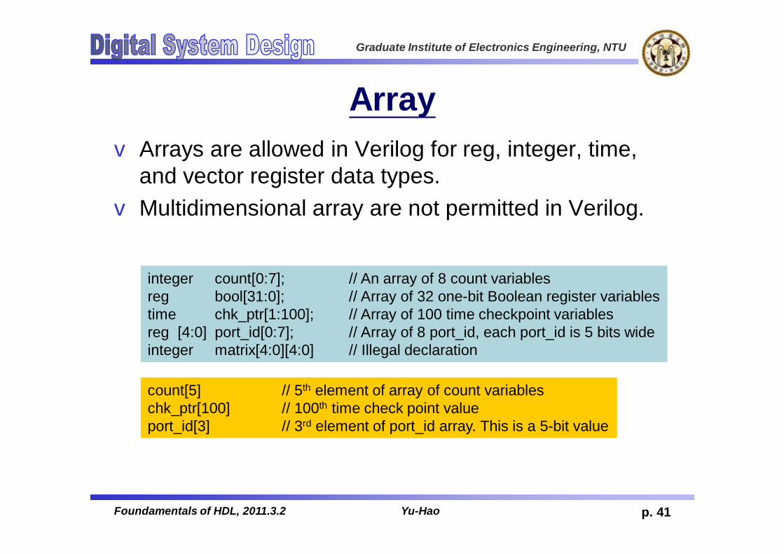
Arrayv Arrays are allowed in Verilog for reg, integer, time,
and vector register data types.vMultidimensional array are not permitted in Verilog.
integer count[0:7]; // An array of 8 count variablesreg bool[31:0]; // Array of 32 one-bit Boolean register variablestime chk_ptr[1:100]; // Array of 100 time checkpoint variablesreg [4:0] port_id[0:7]; // Array of 8 port_id, each port_id is 5 bits wideinteger matrix[4:0][4:0] // Illegal declaration
count[5] // 5th element of array of count variableschk_ptr[100] // 100th time check point valueport_id[3] // 3rd element of port_id array. This is a 5-bit value
p. 41Foundamentals of HDL, 2011.3.2 Yu-Hao

Graduate Institute of Electronics Engineering, NTU
Memoriesv In digital simulation, one often needs to model register files,
RAMs, and ROMs.v Memories are modeled in Verilog simply as an array of registers.v Each element of the array is known as a word, each word can
be one or more bits.v It is important to differentiate between
v n 1-bit registersv One n-bit register
reg mem1bit[0:1023]; // Memory mem1bit with 1K 1-bit wordsreg [7:0] mem1byte[0:1023]; // Memory mem1byte with 1K 8-bit words
mem1bit[255] // Fetches 1 bit word whose address is 255Mem1byte[511] // Fetches 1 byte word whose address is 511
p. 42Foundamentals of HDL, 2011.3.2 Yu-Hao

Graduate Institute of Electronics Engineering, NTU
Arrays Extended after Verilog-2001
v In Verilog-1995, only reg, integer, and time can be declared as array. Array is limited to 1D.
v In Verilog-2001, arrays of real, realtime, and any type of net are allowed.
//bitreg r_1bit;
//vectorreg [3:0] r_4bit_vec;
//1D array: memory: 32bit×8reg [31:0] r_memory [7:0];
//1D array: 8bit×8wire [7:0] w_net [7:0];
//2D array: 4bit×8×8trireg [3:0] row_col_addr [0:7][0:7];
//3D array: 100×16×4 float variablesreal float_array [0:99][1:16][10:13];
p. 43Foundamentals of HDL, 2011.3.2 Yu-Hao

Graduate Institute of Electronics Engineering, NTU
Stringsv String: a sequence of 8-bits ASCII values
v Special characters\n è newline \t è tab character\\ è \ character \” è “ character%% è % character \abc è ASCII code
module string;reg [8*14:1] strvar;initialbegin
strvar = “Hello World”; // stored as 000000486561…726c64strvar = “Hello World!!”; // stored as 00486561…726c642121
endendmodule
p. 44Foundamentals of HDL, 2011.3.2 Yu-Hao
Graduate Institute of Electronics Engineering, NTU
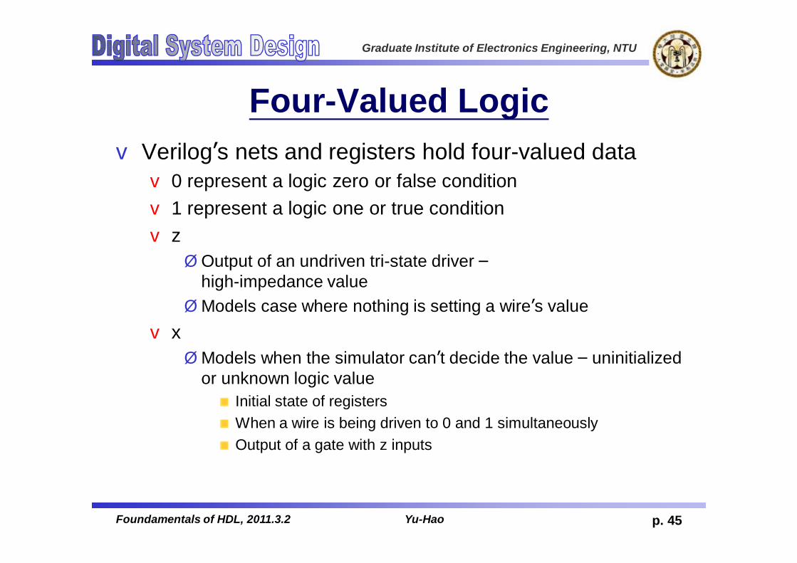
Four-Valued Logicv Verilog’s nets and registers hold four-valued datav 0 represent a logic zero or false conditionv 1 represent a logic one or true conditionv z ØOutput of an undriven tri-state driver –
high-impedance valueØModels case where nothing is setting a wire’s value
v xØModels when the simulator can’t decide the value – uninitialized
or unknown logic valueInitial state of registersWhen a wire is being driven to 0 and 1 simultaneouslyOutput of a gate with z inputs
p. 45Foundamentals of HDL, 2011.3.2 Yu-Hao

Graduate Institute of Electronics Engineering, NTU
Logic System in Verilogv Four values: 0, 1, x or X, z or Z // Not case sensitive here
v The logic value x denotes an unknown (ambiguous) valuev The logic value z denotes a high impedance
v Primitives have built-in logicv Simulators describe 4-value logic (see Appendix A in text)
ab
y
0 1
x
a
b
y
x
xx
z
z z z zx x x x
0 1 X Z0 0 0 0 01 0 1 X XX 0 X X XZ 0 X X X
p. 46Foundamentals of HDL, 2011.3.2 Yu-Hao

Graduate Institute of Electronics Engineering, NTU
Resolution of Contention Between Driversv The value on a wire with multiple drivers in contention may be x
p. 47Foundamentals of HDL, 2011.3.2 Yu-Hao

Graduate Institute of Electronics Engineering, NTU
Logic Strength LevelsvTypes of strengthsvCharge strength: trireg (large>medium>small)vDrive strength: <Net> (supply>strong>pull>weak)
vSyntax
vStrength level
<NetType> <Strength> <Range> <Delay> <Variables>;trireg (large) [1:4] #5 c1;
weakest strongest
highz small medium weak large pull strong supply
p. 48Foundamentals of HDL, 2011.3.2 Yu-Hao

Graduate Institute of Electronics Engineering, NTU
Number Representationv Format: <size>’<base_format><number>v <size> - decimal specification of number of bitsØ default is unsized and machine-dependent but at least 32 bits
v <base format> - ' followed by arithmetic base of numberØ <d> <D> - decimal - default base if no <base_format> givenØ <h> <H> - hexadecimalØ <o> <O> - octalØ <b> <B> - binary
v <number> - value given in base of <base_format>Ø _ can be used for reading clarityØ If first character of sized, binary number 0, 1, x or z, will extend
0, 1, x or z (defined later!)
p. 49Foundamentals of HDL, 2011.3.2 Yu-Hao

Graduate Institute of Electronics Engineering, NTU
Number RepresentationvExamples:v6’b010_111 gives 010111v8’b0110 gives 00000110v4’bx01 gives xx01v16’H3AB gives 0000001110101011v24 gives 0…0011000v5’O36 gives 11100v16’Hx gives xxxxxxxxxxxxxxxxv8’hz gives zzzzzzzz
p. 50Foundamentals of HDL, 2011.3.2 Yu-Hao
Graduate Institute of Electronics Engineering, NTU
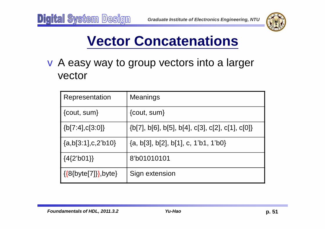
Vector ConcatenationsvA easy way to group vectors into a larger
vector
Representation Meanings
{cout, sum} {cout, sum}
{b[7:4],c[3:0]} {b[7], b[6], b[5], b[4], c[3], c[2], c[1], c[0]}
{a,b[3:1],c,2’b10} {a, b[3], b[2], b[1], c, 1’b1, 1’b0}
{4{2‘b01}} 8‘b01010101
{{8{byte[7]}},byte} Sign extension
p. 51Foundamentals of HDL, 2011.3.2 Yu-Hao

Graduate Institute of Electronics Engineering, NTU
Parameter Declarationv Parameters are not variables, they are constants.
(hardware design view)v Can be defined as a bit or a vectorv Typically parameters are used to specify conditions,
states, width of vector, entry number of array, and delay
module var_mux(out, i0, i1, sel);parameter width = 2, flag = 1’b1;output [width-1:0] out;input [width-1:0] v0, v1;input sel;
assign out = sel==flag ? v1 : v0;endmodule
•If sel = 1, then v1 will be assigned to out;•If sel = 0, then v0 will be assigned to out;
p. 52Foundamentals of HDL, 2011.3.2 Yu-Hao

Graduate Institute of Electronics Engineering, NTU
Overriding the Values of ParametersvModule instance parameter value assignment.v Cannot skip any parameter assignment even you do
not want to reassign it.
module top;……wire [1:0] a_out, a0, a1;wire [3:0] b_out, b0, b1;wire [2:0] c_out, c0, c1;
var_mux U0(a_out, a0, a1, sel);var_mux #(4,2) U1(b_out, b0, b1, sel);var_mux #(3, ) U2(c_out, c0, c1, sel);……
endmodule
The order of assign of parametersfollows the order of declaration of Parameters in the module.
You cannot skip the delay parameter assignment.
p. 53Foundamentals of HDL, 2011.3.2 Yu-Hao

Graduate Institute of Electronics Engineering, NTU
Overriding the Values of Parametersv You can use defparam to group all parameter value
override assignment in one module.
module top;……wire [1:0] a_out, a0, a1;wire [3:0] b_out, b0, b1;wire [2:0] c_out, c0, c1;
var_mux U0(a_out, a0, a1, sel);var_mux U1(b_out, b0, b1, sel);var_mux U2(c_out, c0, c1, sel);
……endmodule
defparamtop.U0.width = 2;top.U0.delay = 1;top.U1.width = 4;top.U1.delay = 2;top.U2.width = 3;top.U2.delay = 1;
p. 54Foundamentals of HDL, 2011.3.2 Yu-Hao

Graduate Institute of Electronics Engineering, NTU
PrimitivesvVerilog has predefined logical elements called
Primitives
vSmallest modeling block for simulatorvBehavior as software execution in simulator, not
hardware description
vVerilog build-in primitive gatevand, or, not, buf, xor, nand, nor, xnorvprim_name inst_name( output, in0, in1,.... );
vUser defined primitive (UDP)vbuilding block defined by designer
p. 55Foundamentals of HDL, 2011.3.2 Yu-Hao

Graduate Institute of Electronics Engineering, NTU
Structural Modelsv Verilog primitives encapsulate pre-defined functionality of common logic gatesv The counterpart of a schematic is a structural model composed of Verilog
primitivesv Model structural detail by instantiating and connecting primitives
module AOI_str (y_out, x_in1, x_in2, x_in3, x_in4, x_in5); output y_out; input x_in1, x_in2, x_in3, x_in4, x_in5; wire y1, y2;
nor (y_out, y1, y2); and (y1, x_in1, x_in2); and (y2, x_in3, x_in4, x_in5);endmodule
y1
y2
x_in1x_in2
x_in3x_in4
y_out
module name module ports
port modes
instantiatedprimitives
primaryinputs
primaryoutput
AOI_str
x_in5
internal wiresestablishconnectivity
p. 56Foundamentals of HDL, 2011.3.2 Yu-Hao
Graduate Institute of Electronics Engineering, NTU
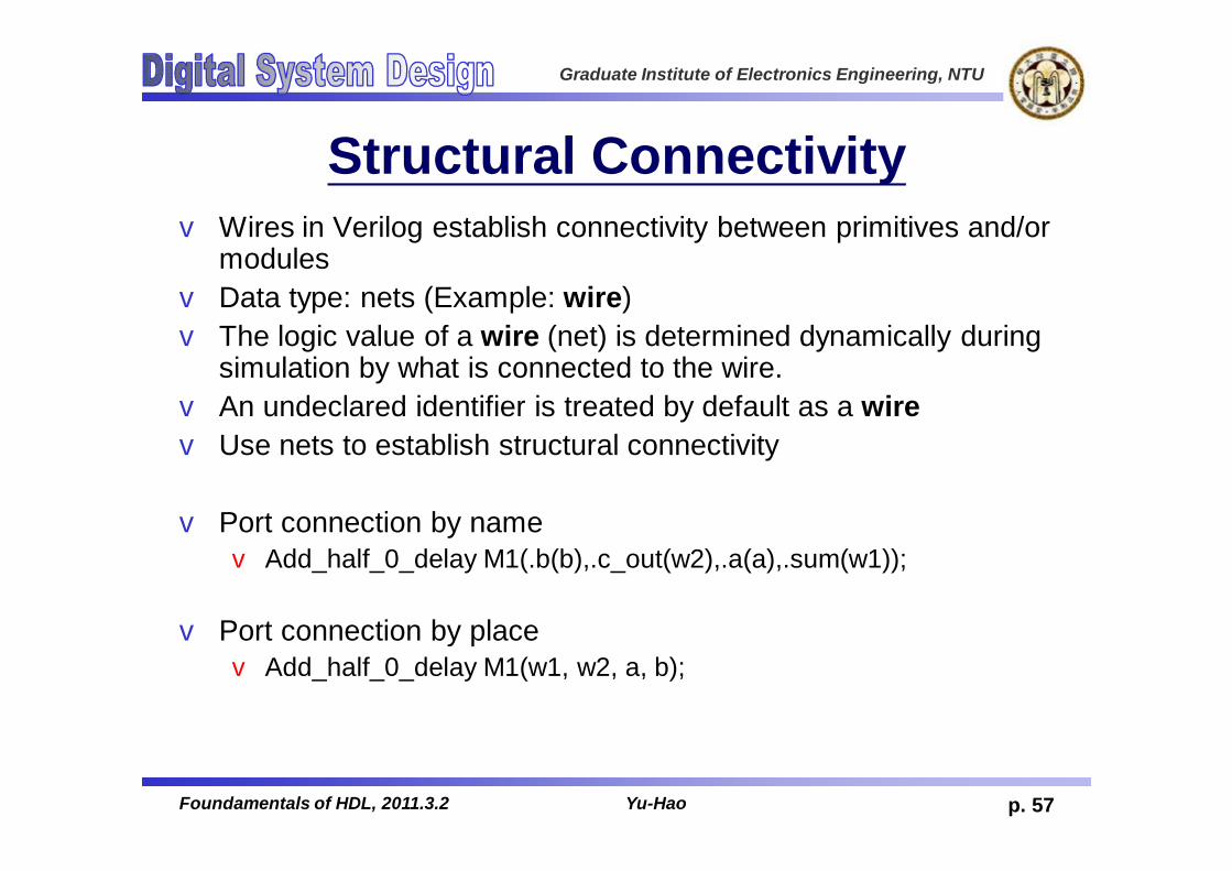
Structural Connectivityv Wires in Verilog establish connectivity between primitives and/or
modulesv Data type: nets (Example: wire)v The logic value of a wire (net) is determined dynamically during
simulation by what is connected to the wire.v An undeclared identifier is treated by default as a wirev Use nets to establish structural connectivity
v Port connection by namev Add_half_0_delay M1(.b(b),.c_out(w2),.a(a),.sum(w1));
v Port connection by placev Add_half_0_delay M1(w1, w2, a, b);
p. 57Foundamentals of HDL, 2011.3.2 Yu-Hao

Graduate Institute of Electronics Engineering, NTU
Hierarchical Design Examplev Model complex structural detail by instantiating modules within modules
a
b c_out
sumAdd_half_0_delay
a
b c_out
sumAdd_half_0_delay
(a ⊕ b) ⊕ c_in
(a + b) c_in + ab
(a⊕ b) c_ina
b
c_in sum
c_out
ab
(a⊕b)
Add_full_0_delay
w1
w2
w3
MODELING TIP
Use nested module instantiations to create a top-downdesign hierarchy.
module Add_full_0_delay (sum, c_out, a, b, c_in); input a, b, c_in; output c_out, sum; wire w1, w2, w3;
Add_half_0_delay M1 (w1, w2, a, b); Add_half_0_delay M2 (sum, w3, c_in, w1); or (c_out, w2, w3);endmodule
module instancename
MODELING TIP
The ports of a module may be listed in any order.The instance name of a module is required.
p. 58Foundamentals of HDL, 2011.3.2 Yu-Hao

Graduate Institute of Electronics Engineering, NTU
Gate and Switch Level Modelingv Coding style: Netlist, connect primitives/modules
by nets (wire)
v Primitives: bottom level of the hierarchyv Verilog Gate Level Primitivesv User-defined Primitives (UDP): described by truth table
v Conventional modulesv Behavior/RTL statementsv Structural statementsv Switch Level Modeling (using transistors)
p. 59Foundamentals of HDL, 2011.3.2 Yu-Hao
Graduate Institute of Electronics Engineering, NTU
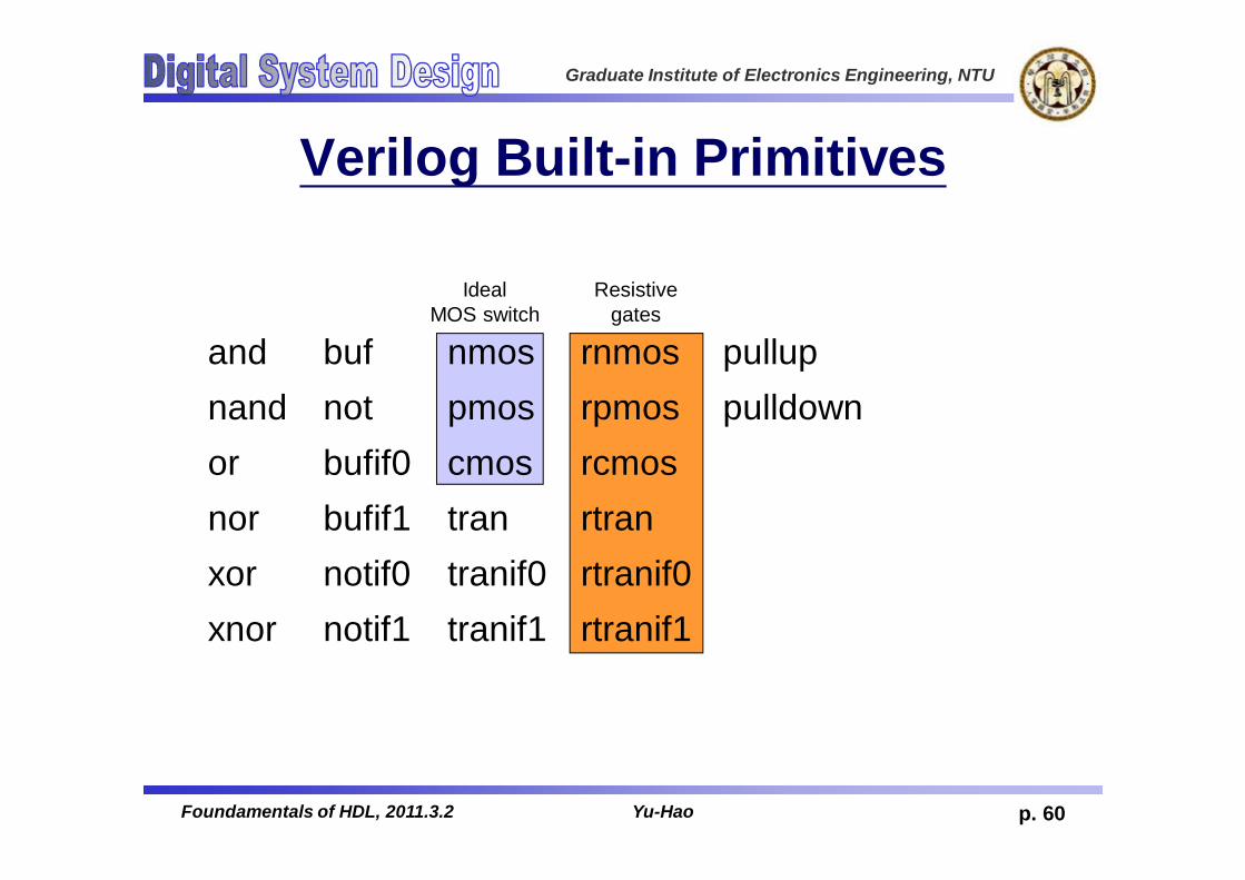
Verilog Built-in Primitives
andnandornorxorxnor
bufnotbufif0bufif1notif0notif1
nmospmoscmostrantranif0tranif1
rnmosrpmosrcmosrtranrtranif0rtranif1
pulluppulldown
IdealMOS switch
Resistivegates
p. 60Foundamentals of HDL, 2011.3.2 Yu-Hao
Graduate Institute of Electronics Engineering, NTU
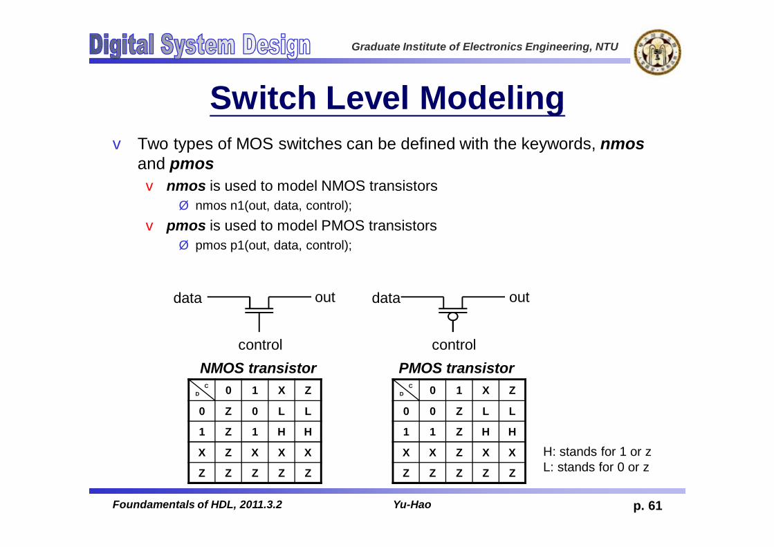
Switch Level Modelingv Two types of MOS switches can be defined with the keywords, nmos
and pmosv nmos is used to model NMOS transistors
Ø nmos n1(out, data, control);v pmos is used to model PMOS transistors
Ø pmos p1(out, data, control);
data dataout out
control controlNMOS transistor PMOS transistor
CD 0 1 X Z
0 Z 0 L L
1 Z 1 H H
X Z X X X
Z Z Z Z Z
CD 0 1 X Z
0 0 Z L L
1 1 Z H H
X X Z X X
Z Z Z Z Z
H: stands for 1 or zL: stands for 0 or z
p. 61Foundamentals of HDL, 2011.3.2 Yu-Hao

Graduate Institute of Electronics Engineering, NTU
CMOS Switchesv CMOS switches are declared with the keyword cmos.v A cmos device can be modeled with a nmos and a
pmos device.v cmos c1(out, data, ncontrol, pcontrol);
v The cmos gate is essentially a combination of two gates: one nmos and one pmos.v nmos n1(out, data, ncontrol);v pmos p1(out, data, pcontrol);
data out
ncontrol
pcontrol
CMOS
p. 62Foundamentals of HDL, 2011.3.2 Yu-Hao

Graduate Institute of Electronics Engineering, NTU
Bidirectional Switchesv NMOS, PMOS, CMOS gates conduct from drain to source.v It is important to have devices that conduct in both directions.v In such cases, signals on either side of the device can be the
driver signal.v Bidirectional switches are typically used to provide isolation
between buses or signals.v tran t1(inout1, inout2);v tranif0 t2(inout1, inout2, control);v tranif1 t3(inout1, inout2, control);
tran tranif1 tranif0
inout1 inout2 inout1 inout2control
inout1 inout2control
p. 63Foundamentals of HDL, 2011.3.2 Yu-Hao

Graduate Institute of Electronics Engineering, NTU
Power and Groundv The power (Vdd, logic 1) and Ground (Vss, logic 0) sources are needed
when transistor-level circuits are designed.v Supply1 are equivalent to Vdd in circuits and place a logical 1 on a net.v Supply0 are equivalent to ground or Vss in circuits and place a logical 0
on a net.
supply1 vdd;supply0 gnd;
assign a = vdd; // connect a to vddassign b = gnd; // connect b to gnd
p. 64Foundamentals of HDL, 2011.3.2 Yu-Hao

Graduate Institute of Electronics Engineering, NTU
Resistive Switchesv Resistive switches have the same syntax as regular switches.v Resistive devices have a high source-to-drain impedance. Regular
switches have a low source-to-drain impedance.v Resistive switches reduce signal strengths when signals pass through.
Regular switches retain strength levels of signals from input to output.
Input Strength Output StrengthSupply Pull
Strong Pull
Pull Weak
Weak Medium
Large Medium
Medium Small
Small Small
High High
p. 65Foundamentals of HDL, 2011.3.2 Yu-Hao
Graduate Institute of Electronics Engineering, NTU
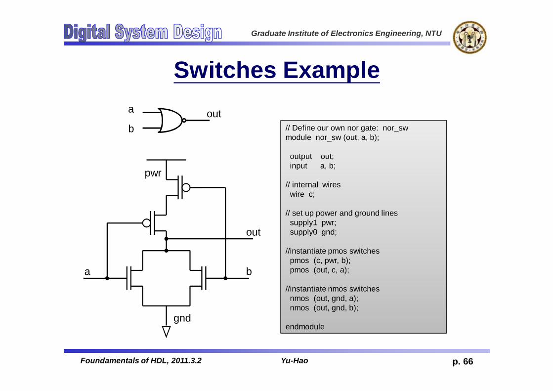
Switches Examplea
bout
out
ba
gnd
pwr
// Define our own nor gate: nor_swmodule nor_sw (out, a, b);
output out;input a, b;
// internal wireswire c;
// set up power and ground linessupply1 pwr;supply0 gnd;
//instantiate pmos switchespmos (c, pwr, b);pmos (out, c, a);
//instantiate nmos switchesnmos (out, gnd, a);nmos (out, gnd, b);
endmodule
p. 66Foundamentals of HDL, 2011.3.2 Yu-Hao

Graduate Institute of Electronics Engineering, NTU
Gate Level ModelingvStepsvDevelope the boolean function of outputvDraw the circuit with logic gates/primitivesvConnect gates/primitives with net (usually wire)
vHDL: Hardware Description LanguagevFigure out architecture first, then write code.
p. 67Foundamentals of HDL, 2011.3.2 Yu-Hao
Graduate Institute of Electronics Engineering, NTU
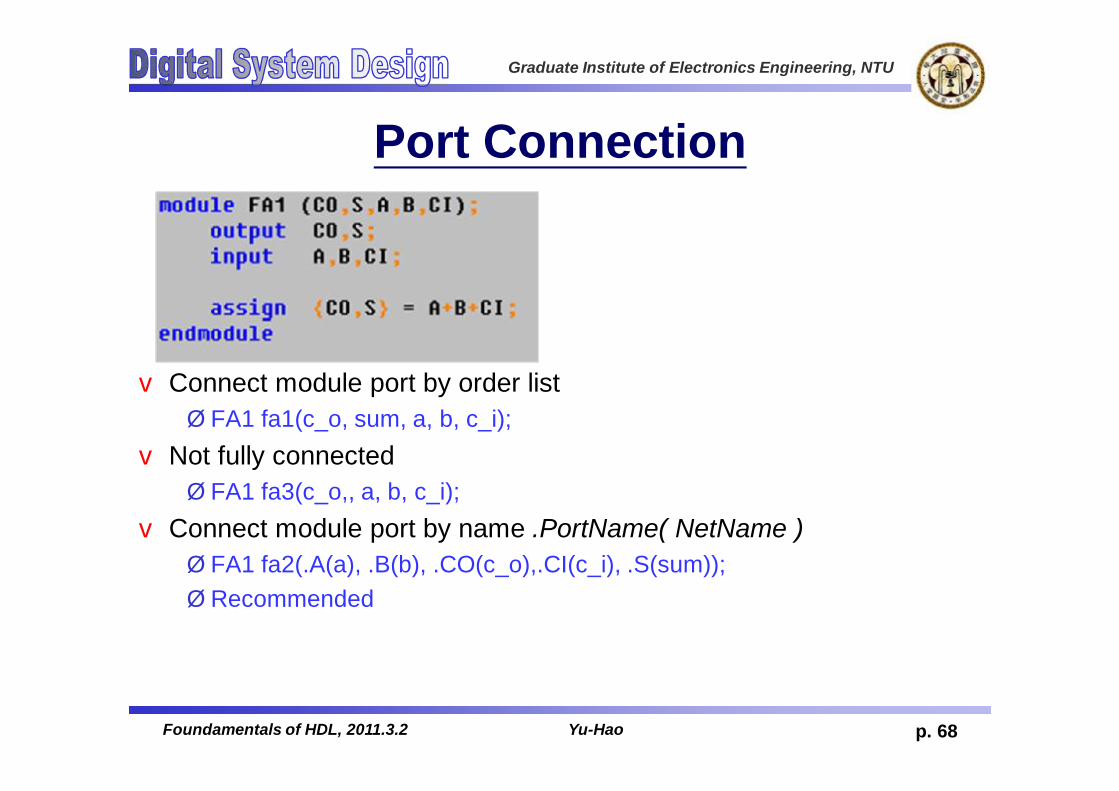
Port Connection
v Connect module port by order listØ FA1 fa1(c_o, sum, a, b, c_i);
v Not fully connectedØ FA1 fa3(c_o,, a, b, c_i);
v Connect module port by name .PortName( NetName ) Ø FA1 fa2(.A(a), .B(b), .CO(c_o),.CI(c_i), .S(sum));ØRecommended
p. 68Foundamentals of HDL, 2011.3.2 Yu-Hao

Graduate Institute of Electronics Engineering, NTU
Case Study1-bit Full Adder
Ci A B SCo
0 0 0 00
0 0 1 10
0 1 0 10
0 1 1 01
1 0 0 10
1 0 1 01
1 1 0 01
1 1 1 11
A B
CiCo
S
FullAdder
p. 69Foundamentals of HDL, 2011.3.2 Yu-Hao

Graduate Institute of Electronics Engineering, NTU
Case Study1-bit Full Adder
v co = (a‧b) + (b‧ci) + (ci‧a);
abbcca
co
p. 70Foundamentals of HDL, 2011.3.2 Yu-Hao
Graduate Institute of Electronics Engineering, NTU
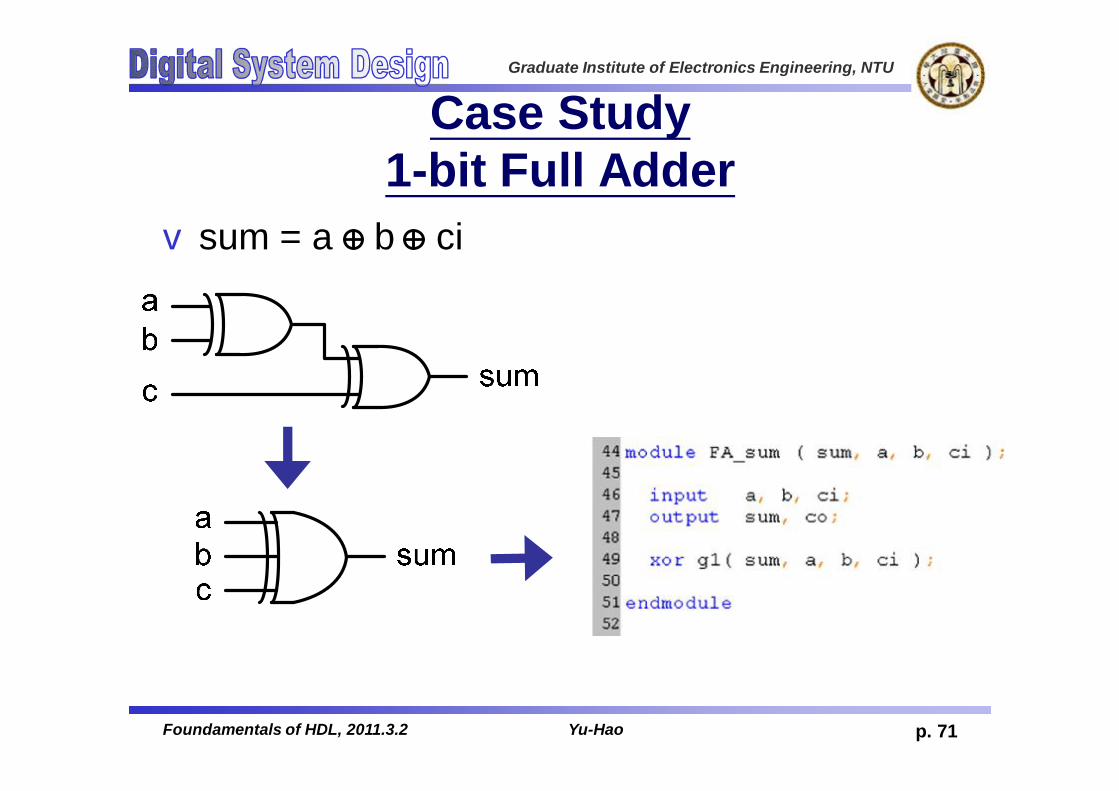
Case Study1-bit Full Adder
vsum = a b ci
p. 71Foundamentals of HDL, 2011.3.2 Yu-Hao
Graduate Institute of Electronics Engineering, NTU
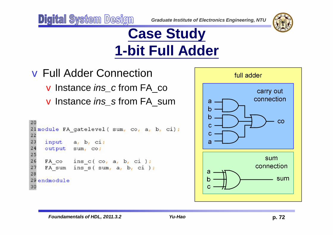
Case Study1-bit Full Adder
vFull Adder ConnectionvInstance ins_c from FA_covInstance ins_s from FA_sum
p. 72Foundamentals of HDL, 2011.3.2 Yu-Hao

Graduate Institute of Electronics Engineering, NTU
Timing and Delayv Functional verification of hardware is used to verify
functionality of the designed circuit.v However, blocks in real hardware have delays
associated with the logic elements and paths in them.v To model these delay, we use timing / delay
description in Verilog: #v Then we can check whether the total circuit meets
the timing requirements, given delay specifications of the blocks.
p. 73Foundamentals of HDL, 2011.3.2 Yu-Hao

Graduate Institute of Electronics Engineering, NTU
Delay Specification in PrimitivesvDelay specification defines the propagation
delay of that primitive gate.
not #10 (out,in);
p. 74Foundamentals of HDL, 2011.3.2 Yu-Hao
Graduate Institute of Electronics Engineering, NTU
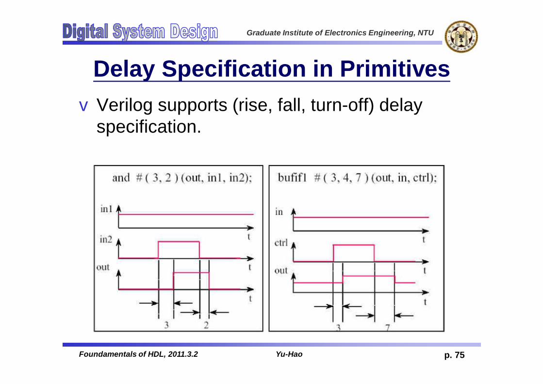
Delay Specification in PrimitivesvVerilog supports (rise, fall, turn-off) delay
specification.
p. 75Foundamentals of HDL, 2011.3.2 Yu-Hao

Graduate Institute of Electronics Engineering, NTU
Delay Specification in Primitivesv All delay specification in Verilog can be specified as
(minimum : typical : maximum) delayv Examplesv (min:typ:max) delay specification of all transitionØ or #(3.2:4.0:6.3) U0(out, in1, in2);
v (min:typ:max) delay specification of RISE transition and FALL transitionØ nand #(1.0:1.2:1.5,2.3:3.5:4.7) U1(out, in1, in2);
v (min:typ:max) delay specification of RISE transition, FALL transition, and turn-off transitionØ bufif1 #(2.5:3:3.4,2:3:3.5,5:7:8) U2(out,in,ctrl);
p. 76Foundamentals of HDL, 2011.3.2 Yu-Hao

Graduate Institute of Electronics Engineering, NTU
Types of Delay Modelsv Distributed Delayv Specified on a per element basicv Delay value are assigned to individual in the circuit
ab
c
d
e
f
out
#5
#7
#4
module and4(out, a, b, c, d);… …and #5 a1(e, a, b);and #7 a2(f, c, d);and #4 a3(out, e, f);
endmodule
p. 77Foundamentals of HDL, 2011.3.2 Yu-Hao

Graduate Institute of Electronics Engineering, NTU
Types of Delay Modelsv Lumped Delayv They can be specified as a single delay on the output gate of
the modulev The cumulative delay of all paths is lumped at one location
ab
c
d
e
f
out#11
module and4(out, a, b, c, d);… …and a1(e, a, b);and a2(f, c, d);and #11 a3(out, e, f);
endmodule
p. 78Foundamentals of HDL, 2011.3.2 Yu-Hao
Graduate Institute of Electronics Engineering, NTU
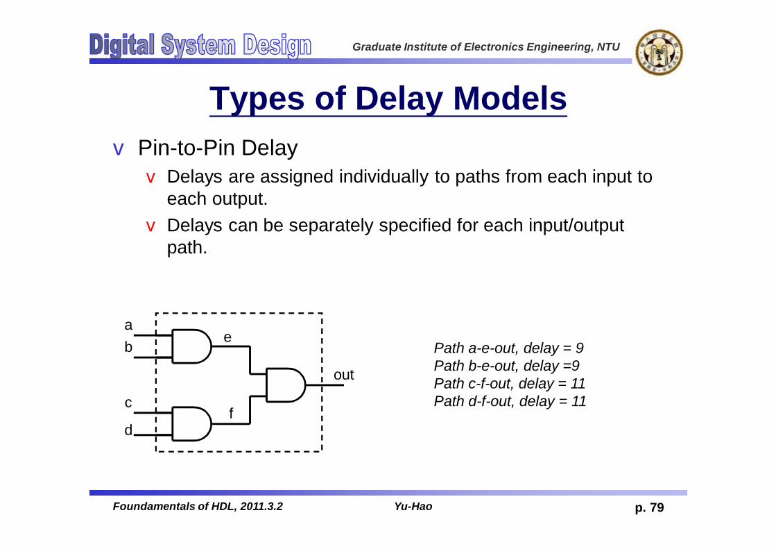
Types of Delay Modelsv Pin-to-Pin Delayv Delays are assigned individually to paths from each input to
each output.v Delays can be separately specified for each input/output
path.
ab
c
d
e
f
out
Path a-e-out, delay = 9Path b-e-out, delay =9Path c-f-out, delay = 11Path d-f-out, delay = 11
p. 79Foundamentals of HDL, 2011.3.2 Yu-Hao

Graduate Institute of Electronics Engineering, NTU
Path Delay Modeling
v Specify blocksv Assign pin-to-pin timing delay
across module pathv Set up timing checks in the
circuitsv Define specparam constants
module and4(out, a, b, c, d);… …// specify block with path delay statementsspecify
(a => out) = 9;(b => out) = 9;(c => out) = 11;(d => out) = 11;
endspecify
// gate instantiationsand a1(e, a, b);and a2(f, c, d);and a3(out, e, f);
endmodule
pp. 80Foundamentals of HDL, 2011.3.2 Yu-Hao

Graduate Institute of Electronics Engineering, NTU
Parallel/Full Connection
(a => out) = 9;(b => out) = 9;(c => out) = 11;(d => out) = 11;
(a,b *> out) = 9;(c,d *> out) = 11;
(a[0] => out[0]) = 9;(a[1] => out[1]) = 9;(a[2] => out[2]) = 9;(a[3] => out[3]) = 9;
(a => out) = 9;
pp. 81Foundamentals of HDL, 2011.3.2 Yu-Hao
Graduate Institute of Electronics Engineering, NTU
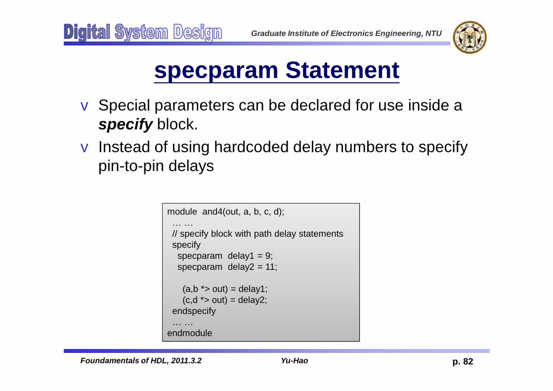
specparam Statementv Special parameters can be declared for use inside a
specify block.v Instead of using hardcoded delay numbers to specify
pin-to-pin delays
module and4(out, a, b, c, d);… …// specify block with path delay statementsspecify
specparam delay1 = 9;specparam delay2 = 11;
(a,b *> out) = delay1;(c,d *> out) = delay2;
endspecify… …
endmodule
p. 82Foundamentals of HDL, 2011.3.2 Yu-Hao
Graduate Institute of Electronics Engineering, NTU
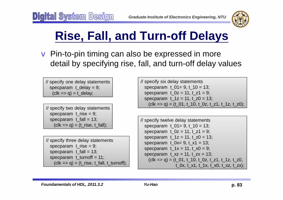
Rise, Fall, and Turn-off Delaysv Pin-to-pin timing can also be expressed in more
detail by specifying rise, fall, and turn-off delay values
// specify one delay statementsspecparam t_delay = 9;
(clk => q) = t_delay;
// specify two delay statementsspecparam t_rise = 9;specparam t_fall = 13;
(clk => q) = (t_rise, t_fall);
// specify three delay statementsspecparam t_rise = 9;specparam t_fall = 13;specparam t_turnoff = 11;
(clk => q) = (t_rise, t_fall, t_turnoff);
// specify six delay statementsspecparam t_01= 9, t_10 = 13;specparam t_0z = 11, t_z1 = 9;specparam t_1z = 11, t_z0 = 13;
(clk => q) = (t_01, t_10, t_0z, t_z1, t_1z, t_z0);
// specify twelve delay statementsspecparam t_01= 9, t_10 = 13;specparam t_0z = 11, t_z1 = 9;specparam t_1z = 11, t_z0 = 13;specparam t_0x= 9, t_x1 = 13;specparam t_1x = 11, t_x0 = 9;specparam t_xz = 11, t_zx = 13;
(clk => q) = (t_01, t_10, t_0z, t_z1, t_1z, t_z0,t_0x, t_x1, t_1x, t_x0, t_xz, t_zx);
p. 83Foundamentals of HDL, 2011.3.2 Yu-Hao

Graduate Institute of Electronics Engineering, NTU
Min, Max, and Typical DelaysvMin, max, and typical delay value were discussed
earlier for gatesv Can also be specified for pin-to-pin delays.
// specify two delay statementsspecparam t_rise = 8:9:10;specparam t_fall = 12:13:14;specparam t_turnoff = 10:11:12
(clk => q) = (t_rise, t_fall, t_turnoff);
p. 84Foundamentals of HDL, 2011.3.2 Yu-Hao

Graduate Institute of Electronics Engineering, NTU
Timing Checks - For Testbenchv setup time and hold time
checks
setuptime
holdtime
clock
data
specify $setup(data, posedge clock, 3);
endspecify
specify $hold(posedge clock, data, 5);
endspecify
vWidth checkv Sometimes it is
necessary to check the width of a pulse.
width ofthe pulse
clock
specify $width(posedge clock, 6);
endspecify
p. 85Foundamentals of HDL, 2011.3.2 Yu-Hao

Graduate Institute of Electronics Engineering, NTU
OutlinevOverview and HistoryvHierarchical Design MethodologyvLevels of ModelingvBehavioral Level ModelingvRegister Transfer Level (RTL) Modeling vStructural/Gate Level Modeling
vLanguage ElementsvLogic GatesvData TypevTiming and Delay
vSimulation & Verification
p. 86Foundamentals of HDL, 2011.3.2 Yu-Hao

Graduate Institute of Electronics Engineering, NTU
Verification Methodology v Task: systematically verify the functionality of a model.v Approaches: Simulation and/or formal verificationv Simulation:
(1) detect syntax violations in source code(2) simulate behavior(3) monitor results
Unit_Under_Test (UUT)
StimulusGenerator
ResponseMonitor
Design_Unit_Test_Bench (DUTB)
D
Q
QSET
CLR
p. 87Foundamentals of HDL, 2011.3.2 Yu-Hao

Graduate Institute of Electronics Engineering, NTU
Components of a Simulation
Stimulus Block
Design Block
OutputResults
InputPatterns
Dummy Top Block
DesignBlock
StimulusBlock
OutputResults
InputPatterns
The output results are verified by console/waveform viewer
The output results are verified by testbench or stimulus block
pp. 88Foundamentals of HDL, 2011.3.2 Yu-Hao

Graduate Institute of Electronics Engineering, NTU
Verilog Simulator
p. 89Foundamentals of HDL, 2011.3.2 Yu-Hao
Graduate Institute of Electronics Engineering, NTU
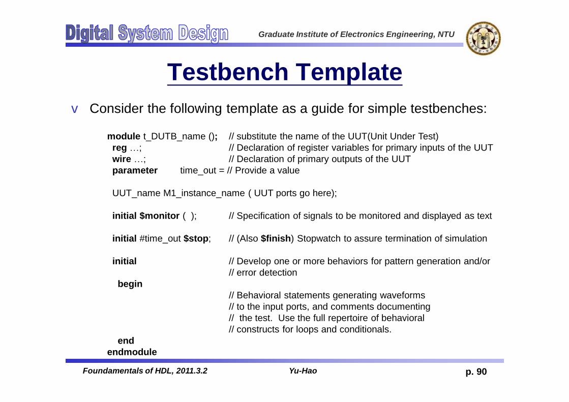
Testbench Template v Consider the following template as a guide for simple testbenches:
module t_DUTB_name (); // substitute the name of the UUT(Unit Under Test)reg…; // Declaration of register variables for primary inputs of the UUTwire…; // Declaration of primary outputs of the UUTparameter time_out = // Provide a value
UUT_name M1_instance_name ( UUT ports go here);
initial $monitor ( ); // Specification of signals to be monitored and displayed as text
initial #time_out $stop; // (Also $finish) Stopwatch to assure termination of simulation
initial // Develop one or more behaviors for pattern generation and/or// error detection
begin// Behavioral statements generating waveforms // to the input ports, and comments documenting// the test. Use the full repertoire of behavioral // constructs for loops and conditionals.
endendmodule
p. 90Foundamentals of HDL, 2011.3.2 Yu-Hao
Graduate Institute of Electronics Engineering, NTU
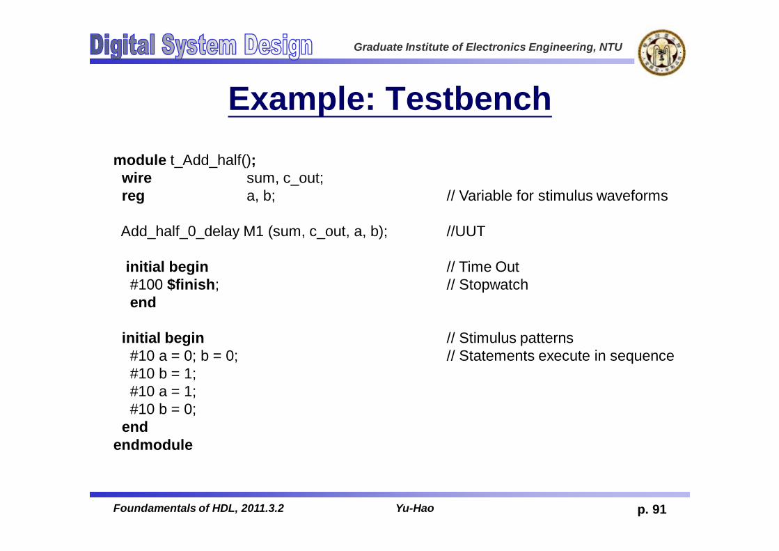
Example: Testbenchmodule t_Add_half();
wire sum, c_out;reg a, b; // Variable for stimulus waveforms
Add_half_0_delay M1 (sum, c_out, a, b); //UUT
initial begin // Time Out#100 $finish; // Stopwatchend
initial begin // Stimulus patterns#10 a = 0; b = 0; // Statements execute in sequence#10 b = 1; #10 a = 1;#10 b = 0;
endendmodule
p. 91Foundamentals of HDL, 2011.3.2 Yu-Hao

Graduate Institute of Electronics Engineering, NTU
Behaviors for Abstract Models v Verilog has three types of behaviors for composing abstract models of
functionality v Continuous assignment (Keyword: assign) -- laterv Single pass behavior (Keyword: initial) -- Note: only use in testbenchesv Cyclic behavior (Keyword: always) -- later
v Single pass and cyclic behaviors execute procedural statements like aprogramming language
v The procedural statements execute sequentiallyv A single pass behavior expires after the last statement executesv A cyclic behavior begins executing again after the last statement
executes
p. 92Foundamentals of HDL, 2011.3.2 Yu-Hao
Graduate Institute of Electronics Engineering, NTU
Signal Generatorsv Use cyclic behaviors to describe stimulus generators v Statements in a behavior may be grouped in begin … end blocks v Execution begins at tsim = 0 v # delay control operator temporarily suspends execution of a behavior v The operator = denotes procedural assignment (also called blocking
assignment)
MODELING TIP
Use procedural assignments to describe stimulus patterns ina testbench.
p. 93Foundamentals of HDL, 2011.3.2 Yu-Hao
Graduate Institute of Electronics Engineering, NTU
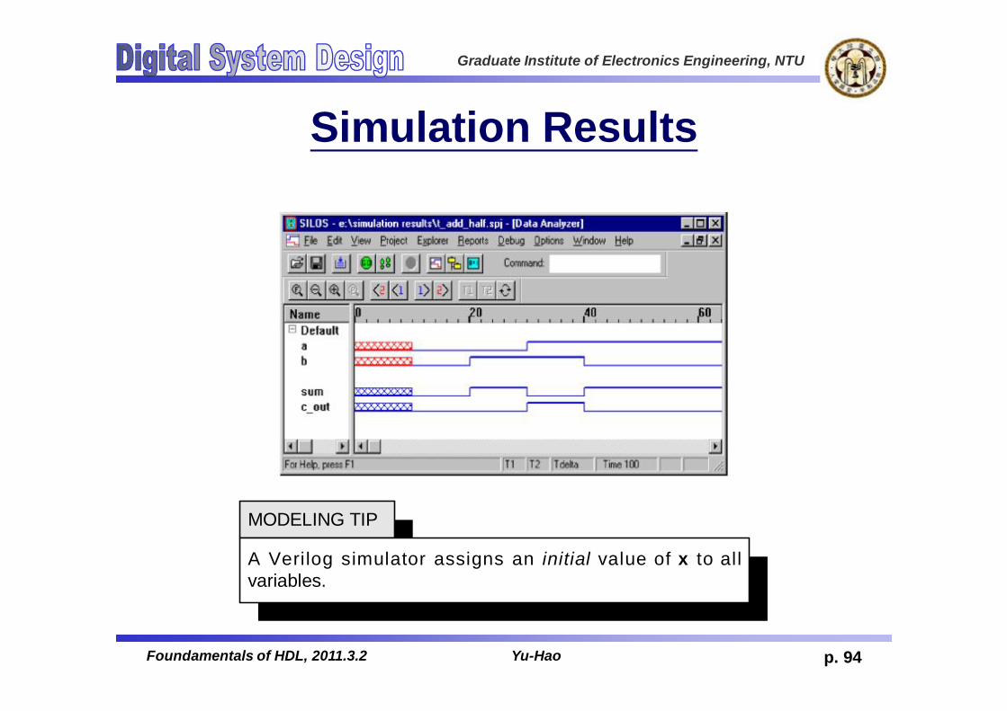
Simulation Results
MODELING TIP
A Verilog simulator assigns an initial value of x to allvariables.
p. 94Foundamentals of HDL, 2011.3.2 Yu-Hao
Graduate Institute of Electronics Engineering, NTU
Propagation Delay v Gate propagation delay specifies the time between an input
change and the resulting output change v Transport delay describes the time-of-flight of a signal transition v Verilog uses an inertial delay model for gates and transport
delay for nets v Inertial delay suppresses short pulses (width less than the
propagation delay value) v Inertial delay:the amount of time that the inputs must be stable
in order to generate an output
MODELING TIP
All primitives and nets have a default propagation delay of 0.
p. 95Foundamentals of HDL, 2011.3.2 Yu-Hao
Graduate Institute of Electronics Engineering, NTU
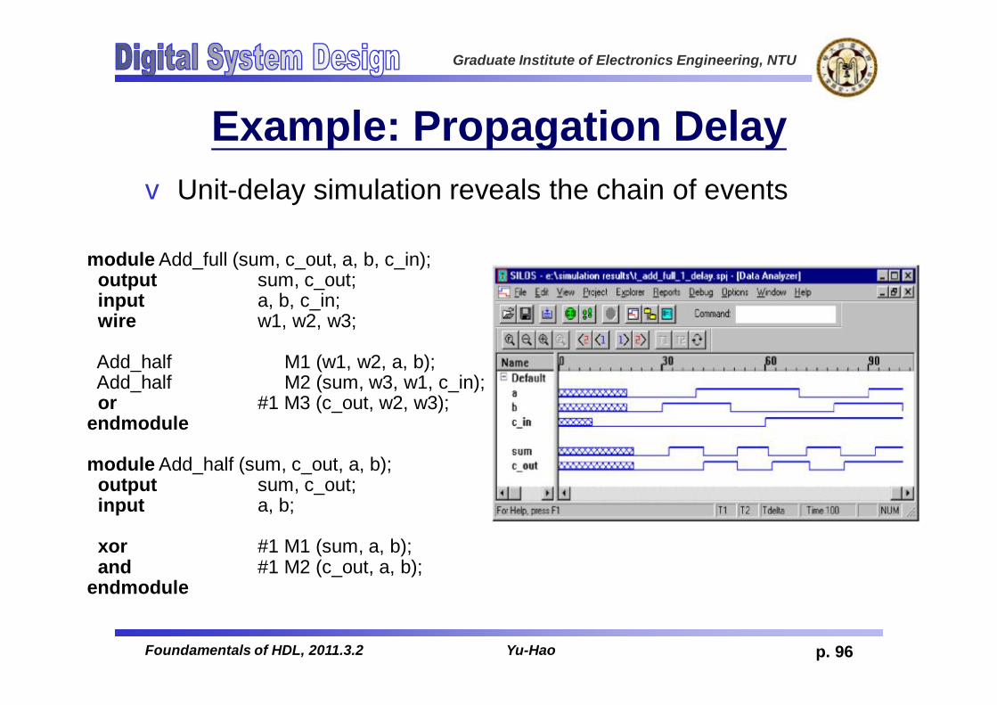
Example: Propagation Delay v Unit-delay simulation reveals the chain of events
module Add_full (sum, c_out, a, b, c_in);output sum, c_out;input a, b, c_in;wire w1, w2, w3;
Add_half M1 (w1, w2, a, b);Add_half M2 (sum, w3, w1, c_in);or #1 M3 (c_out, w2, w3);
endmodule
module Add_half (sum, c_out, a, b);output sum, c_out;input a, b;
xor #1 M1 (sum, a, b); and #1 M2 (c_out, a, b);
endmodule
p. 96Foundamentals of HDL, 2011.3.2 Yu-Hao
Graduate Institute of Electronics Engineering, NTU
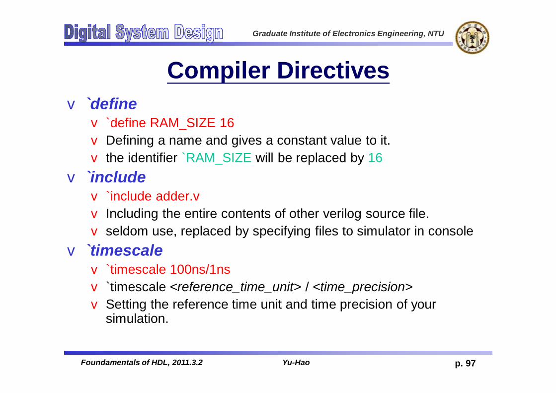
Compiler Directives v `definev `define RAM_SIZE 16v Defining a name and gives a constant value to it.v the identifier `RAM_SIZE will be replaced by 16
v `includev `include adder.vv Including the entire contents of other verilog source file.v seldom use, replaced by specifying files to simulator in console
v `timescalev `timescale 100ns/1nsv `timescale <reference_time_unit> / <time_precision>v Setting the reference time unit and time precision of your
simulation.
p. 97Foundamentals of HDL, 2011.3.2 Yu-Hao
Graduate Institute of Electronics Engineering, NTU
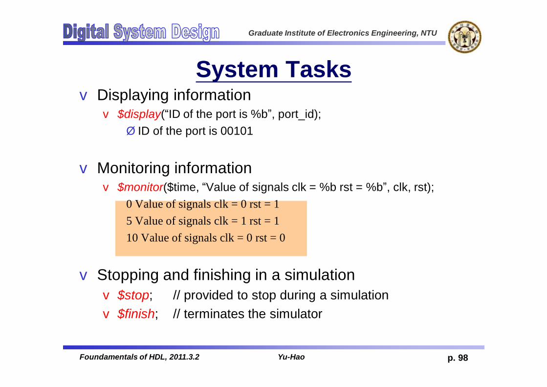
System Tasksv Displaying informationv $display(“ID of the port is %b”, port_id);Ø ID of the port is 00101
vMonitoring informationv $monitor($time, “Value of signals clk = %b rst = %b”, clk, rst);
0 Value of signals clk = 0 rst = 15 Value of signals clk = 1 rst = 110 Value of signals clk = 0 rst = 0
v Stopping and finishing in a simulationv $stop; // provided to stop during a simulationv $finish; // terminates the simulator
p. 98Foundamentals of HDL, 2011.3.2 Yu-Hao

Graduate Institute of Electronics Engineering, NTU
Simulation SchemesvThere are 3 categories of simulation schemesvTime-based: Simulation on real time scale, used
by SPICE simulatorsvEvent-based: Simulation on events of signal
transition, used by Verilog simulators. Note each event must occurs on discrete time specified by the testbench.vCycle-based: Used by system/platform level
verification, less used in cell-based IC designing.
p. 99Yu-HaoFoundamentals of HDL, 2011.3.2

Graduate Institute of Electronics Engineering, NTU
Time Wheel Concept in Event-Based Simulation
p. 100Yu-HaoFoundamentals of HDL, 2011.3.2


