P
a
g
e
Find us at www.keysight.com Page 1
8762/3/4A, B, C Coaxial Switches High performance switches for microwave and RF instrumentation and systems
Keysight Technologies, Inc. offers a versatile line of multiport coaxial switches. These 50Ω
mechanical-latching switches come with the performance and reliability that you have come to
expect in Keysight microwave accessories.
Offering excellent electrical and mechanical performance with broadband operation, high
isolation, low SWR, long life, and exceptional repeatability, these switches are designed with
your applications in mind. Frequency ranges are available to 4 GHz and 18 GHz for the A and
B models with SMA connectors and to 26.5 GHz for the C models with APC-3.5 connectors.
P
a
g
e
Find us at www.keysight.com Page 2
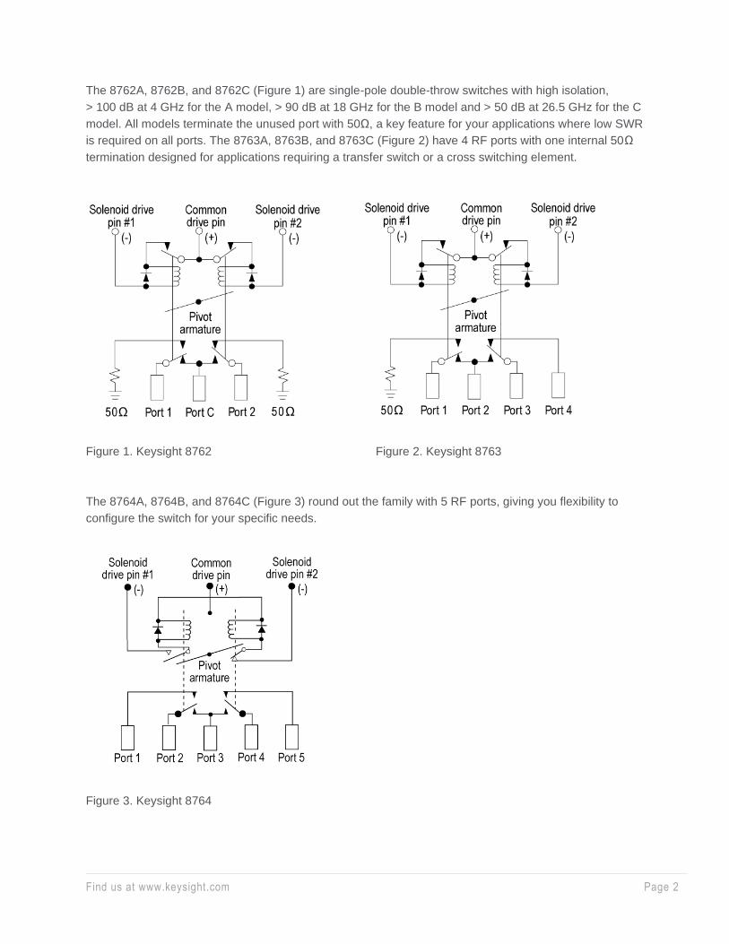
The 8762A, 8762B, and 8762C (Figure 1) are single-pole double-throw switches with high isolation,
> 100 dB at 4 GHz for the A model, > 90 dB at 18 GHz for the B model and > 50 dB at 26.5 GHz for the C
model. All models terminate the unused port with 50Ω, a key feature for your applications where low SWR
is required on all ports. The 8763A, 8763B, and 8763C (Figure 2) have 4 RF ports with one internal 50Ω
termination designed for applications requiring a transfer switch or a cross switching element.
Figure 1. Keysight 8762 Figure 2. Keysight 8763
The 8764A, 8764B, and 8764C (Figure 3) round out the family with 5 RF ports, giving you flexibility to
configure the switch for your specific needs.
Figure 3. Keysight 8764

P
a
g
e
Find us at www.keysight.com Page 3
Applications
Multi-source switching
The 8762A, 8762B or 8762C is an excellent choice for applications where you require selection of
multiple signal sources, frequency counters, or signal control devices such as modulators or filters, or
routing signals from multiple sources as shown in Figure 4.
Figure 4. Multi-source switching
Transfer switching
For applications requiring a “transfer switch,” as shown in Figure 5, an 8763A, B, or C is the ideal choice
to insert a component, such as a filter or mixer, into a signal path. Another popular use is to switch
between a device under test and a through path for system calibration. The 8763A,B,C’s internal load can
terminate the device under test when in the through mode (up to 1 watt).
Figure 5. Keysight 8763 used as a transfer switch (equivalent circuit action)
P
a
g
e
Find us at www.keysight.com Page 4
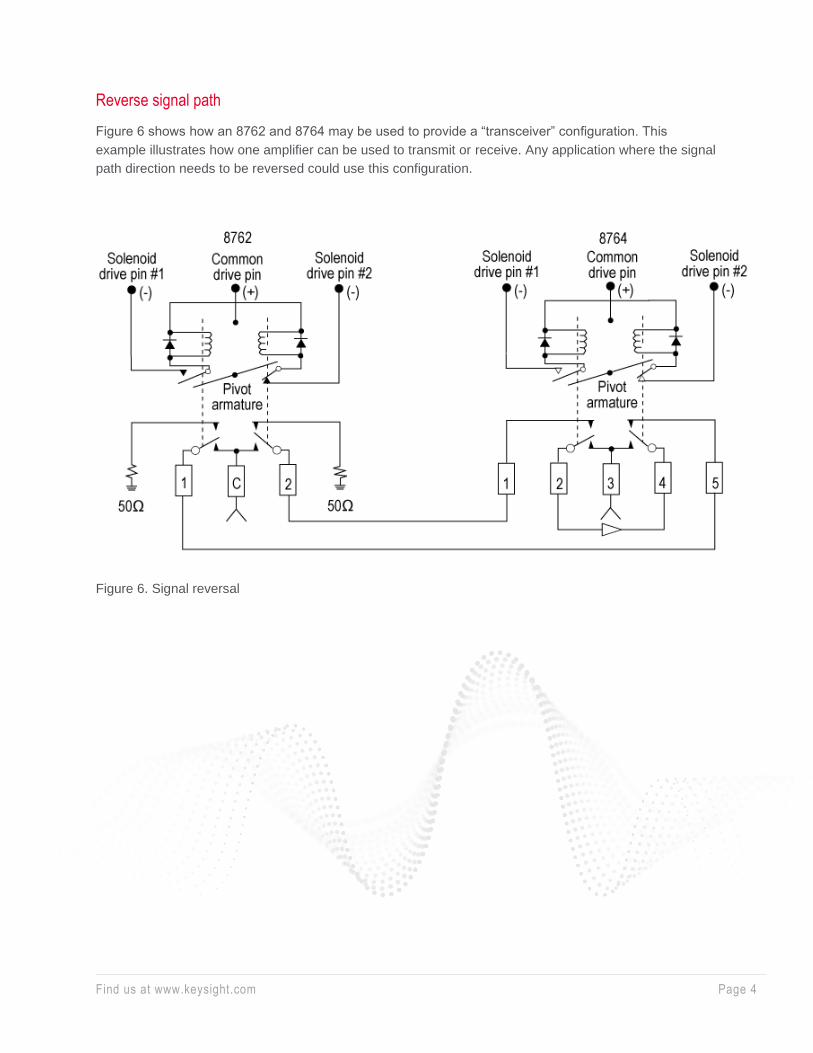
Reverse signal path
Figure 6 shows how an 8762 and 8764 may be used to provide a “transceiver” configuration. This
example illustrates how one amplifier can be used to transmit or receive. Any application where the signal
path direction needs to be reversed could use this configuration.
Figure 6. Signal reversal

P
a
g
e
Find us at www.keysight.com Page 5
Portable and remote applications
Due to their small package size, light weight, low power consumption, and high reliability, these
switches are ideal for your portable or remote applications. The light weight and repeatability make
them well suited for portable spectrum analyzers and other portable microwave test equipment.
Their 1,000,000 cycle life make them the ideal candidate for system design, such as
communications repeaters or remote monitoring stations that demand minimal maintenance. The
switch’s automatic coil disconnect feature and low current drain during switching minimize the
amount of power needed for operating the switches.
Dedicated switching
For larger switching systems, where many switches will be used to provide complex signal routing, a
switch driver such as the 87130A or 70611A is recommended. The 87130A rack-and-stack switch
driver and the MMS-based 70611A are convenient, flexible interface bus (GPIB) or modular systems
interface bus (MS-IB) switch controllers, providing driver circuitry, indicator readback circuitry and
firmware that makes it easy to integrate switch components into a switching system. Controlling the
87130A is simple using either a PC or workstation based GPIB controller and Keysight Interactive
Test Generator (Keysight-ITG) or Keysight Visual Engineering Environment (Keysight VEE). The
70611A gives manual control via the MMS user interface or can also be controlled via an GPIB
equipped PC or workstation.
In addition, the built-in firmware makes it possible to define often used switch paths. With the path
command, macros can be designed which open and close the right solenoids to select the desired
switch port, and the path may be given a meaningful name. Remember that only one select pin
should be activated at one time to prevent rapid cycling of the switch.
Both the 87130A and 70611A provide position monitoring and reporting, which make it possible for a
program to determine if all the switches are in their proper state (position) before the program
continues with testing. A programmable wake up condition makes it possible to ensure that the
matrix or switching system starts up in a predetermined state, to prevent damage to delicate
equipment from excessive power. This would also be the state that the system returns to after a
power interruption.
Accessory cables and adapters make it easy to quickly get the 8762/3/4 working with the 87130A or
70611A. Reference literature number 5963-2038E, Switch Attenuator Driver Configuration Guide.
For smaller switching needs, the 11713B/C attenuator/switch controller provides simple GPIB control
for up to ten 8762/3/4 switches. Connecting cables can be ordered which make it easy to connect
the switches to the 11713B/C. Refer to literature number 5958-7277EN, Keysight 11713B/C
Attenuator/Switch Drivers Configuration Guide.

P
a
g
e
Find us at www.keysight.com Page 6
Operation and use
How the switch works
All the switches are “break before make;” the switched ports are not connected to each other preventing
possible damage to sensitive circuits. The standard configuration switch uses 24 Vdc for the switching
voltage, Option 876xx-0111 specifies a voltage of 5 Vdc, and Option 876xx-015 specifies 15 Vdc. Options
876xx-T15 and 876xx-T24 are TTL/5V CMOS compatible with 15 Vdc and 24 Vdc drive respectively.
Driving the switch
For standard, Options 876xx-011 and 876xx-015 switches, switching is accomplished by applying the
supply voltage to pin “C” and grounding the appropriate pin to actuate the switching mechanism.
Avoid grounding both RF path select pins as rapid cycling may occur. After the switch is fully
latched (30 ms), the drive current is automatically disconnected. If the drive circuit is pulsed, the pulse
duration must be at least 30 ms to ensure that the switch will fully latch. For TTL/5 volt CMOS
compatible drive (Options 876xx-T24 and 876xx-T15), apply the supply voltage to pin “C,” and ground
to pin #1. Switch positions by applying a TTL “high” or TTL “low” to pin #2 as needed. See Table 1.
Remote indication (TTL options excluded)
The position of the switch may be determined by utilizing the open and closed states of the internal coil
contacts. Figure 7 displays two indicator circuits, one to provide a TTL output and one that directly
activates an LED. The circuits will output a TTL “HI” and LED “on” if the switch is in the state shown in
Figure 7. When drive pin 1 contact is closed (as shown), RF port 2 is connected to common port. For the
Keysight 8763/4, see Figures 2, 3, and Table 1 for corresponding RF port connections. The circuits
shown are designed to operate with coil voltage of 24 V. If other voltage switches are used, the circuit
components must be modified to accommodate that voltage.
Since current is drawn through the solenoid for these indicator circuits, inadvertent switching is prevented
by limiting the current to 5 mA. Additional design information may be required from the component
manufacturer for the circuits described in Figure 7, depending upon specific applications.

P
a
g
e
Find us at www.keysight.com Page 7
Figure 7. TTL and LED remote indicator circuits
Keysight assumes no responsibility for use of any circuits described herein, and makes no
representations or warranties, expressed or implied, that such circuits are free from patent infringements.

P
a
g
e
Find us at www.keysight.com Page 8
Table 1. Switching logic table
Standard drive TTL drive 1
Model number Pin 1 Pin 2 Pin 2 2 RF path
8762A/B/C
Ground Open TTL high 1 to C closed
2 terminated
Open Ground TTL low 2 to C closed
1 terminated
8763A/B/C
Ground Open TTL high 1 to 2 closed
3 to 4 closed
Open Ground TTL low
1 terminated
2 to 3 closed
4 Open
8764A/B/C
Ground Open TTL high
1 Open
2 to 3 closed
4 to 5 closed
Open Ground TTL low
1 to 2 closed
3 to 4 closed
5 Open
Figure 7. Control voltage states

P
a
g
e
Find us at www.keysight.com Page 9
Specifications
Keysight model numbers 8762A, 8763A, 8764A 8762B, 8763B, 8764B 8762C, 8763C, 8764C
Frequency range dc to 4 GHz dc to 18 GHz dc to 26.5 GHz
Insertion loss < 0.20 dB, dc to 2 GHz
< 0.25 dB, 2 to 4 GHz
< 0.20 dB, dc to 2 GHz
< 0.50 dB, 2 to 18 GHz
< 0.25 dB, dc to 2 GHz
< 0.50 dB, 2 to 18 GHz
< 1.25 dB, 18 to 26.5 GHz
Isolation between ports > 100 dB, dc to 4 GHz > 90 dB, dc to 18 GHz > 90 dB, dc to 18 GHz
> 50 dB, 18 to 26.5 GHz
SWR through line < 1.10, dc to 2 GHz
< 1.20, 2 to 4 GHz
< 1.10, dc to 2 GHz
< 1.20, 2 to 12.4 GHz
< 1.30, 12.4 to 18 GHz
< 1.15, dc to 2 GHz
< 1.25, 2 to 12.4 GHz
< 1.40, 12.4 to 18 GHz
< 1.80, 18 to 26.5 GHz
Into internal 50Ω load
(8762s and 8763s)
< 1.10, dc to 2 GHz
< 1.20, 2 to 4 GHz
< 1.10, dc to 2 GHz
< 1.20, 2 to 12.4 GHz
< 1.15, dc to 2 GHz
< 1.25, 2 to 12.4 GHz
< 1.30, 12.4 to 18 GHz
< 1.80, 18 to 26.5 GHz
Connectors SMA (f) SMA (f) 3.5 mm (f)
Insertion loss repeatability
dc to 18 GHz 18 to 26.5
GHz (Up to 1,000,000
cycles measured at 25 °C)
0.03 dB typical 0.03 dB typical 0.03 dB typical
0.05 dB typical
General operating data
Maximum power rating
Life
Switching solenoid
1 watt average; 100 watts peak (not to exceed average power rating); +7 Vdc
1,000,000 cycles typical
Switching speed 30 ms maximum

P
a
g
e
Find us at www.keysight.com Page 10
Switch drive data
Parameter Test conditions Minimum Nominal Maximum Units
Supply voltage
Option 876xx-024 or 876xx-T24
Options 876xx-015/876xx-T15
Option 876xx-011
20
12
4.5
24
15
5
32
20
7
V
V
v
Supply current Switching; pulse width ≥ 30 ms maximum
Option 876xx-024 or 876xx-T24
Options 876xx-015/876xx-T15
Option 876xx-011
@ Vcc = 24 Vdc
@ Vcc = 15 Vdc
@ Vcc = 5 Vdc
120
182
400
mA
mA
mA
Impedance
Option 876xx-024 or 876xx-T24 200
127
Ohm
mH
Option 876xx-015, Option 876xx-T15 82
57
Ohm
mH
Option 876xx-011 13
8
Ohm
mH
Options 876xx-T15 and 876xx-T24
High-level input
Low-level input
Max high input current
Supply current (quiescent)
Vcc = Max
Vinput = 7.0 Vdc
Vinput = 0.0
Vinput = 7.0
3
0.4
300
2.0
50
V
V
µA
mA
µA
Environmental
Operating
temperature
–25 to +75 °C
Humidity
99% RH, 40°C,
5 days
Vibration
0.05”,
10 to 55 Hz
Shock
50 g’s,
3 ms
Physical specifications
Dimensions
Weight
Per Figure 9
245 g (9 oz.)

P
a
g
e
Find us at www.keysight.com Page 11
Keysight 8762 Series Keysight 8763/64 Series
Figure 9. Product outlines

P
a
g
e
Find us at www.keysight.com Page 12
Learn more at: www.keysight.com
For more information on Keysight Technologies’ products, applications or services,
please contact your local Keysight office. The complete list is available at:
www.keysight.com/find/contactus
This information is subject to change without notice. © Keysight Technologies, 2017 - 2020, Published in USA, April 13, 2020, 5952-1873E
Ordering Information
Model no. Frequency range Option
8762A/B/C
8763A/B/C
8764A/B/C
A models: 4 GHz
B models: 18 GHz
C models: 26.5 GHz
Option 011: 5 Vdc
Option 015: 15 Vdc
Option 024: 24 Vdc
Option T15: TTl/5V CMOS compatible with 15 Vdc supply
Option T24: TTL/5V CMOS compatible with 24 Vdc supply
Option UK6: Commercial calibration test data with certificate
Related Literature
Keysight RF and Microwave Switch Selection Guide, literature number 5989-6031EN


