e-beam lithography - ::: 歡迎光臨中興大學物理系, …ezphysics.nchu.edu.tw/ctsp/e-beam...
TRANSCRIPT

E-beam lithography

Lithography 8^·�
平版印刷是由波西米亞的阿羅斯!塞尼菲爾德 (Alois Senefelder) 於1798年發明的
版模 成品
在電子製造中,我們把設計圖,轉移到材料上形成電子結構的過程稱做微影術

Novel nanolithography techniques
E-beam FIB SPM
Direct writing Low throughput
Imprinting

ÚDÿcDÚĊ·�設計的圖案尺度在微米與奈米等級 現有的成熟技術包括
6]� ï�OÚĊ�
cDĥ8�
¬øª� ÚĊ·�

²ÝĦ2ÚĊ·o$y'ì�
Method 方法 Feature Size ( mm) 尺寸大小
UV Photolithography UV光刻 1 Laser DWW 雷射直寫 1-2 Electron Beam 電子束 0.25-0.1 (可以更小)
Ion Beam 離子束 0.05-0.1 X-Ray Lithography X光刻 <0.1
光刻技術的進展

6äÿÌ6ä&m mask and maskless techniques
使用光罩的微影術 不使用光罩的微影術 直寫技術(direct writing)
電子束微影,離子束微影 ,雷射束
一般光刻方法
M.A.Schimdt MIT opencourse 3.155J/6.152J

6]ĂG|Î�
正光阻
矽晶片
二氧化矽 正光阻
曝光
顯影
蝕刻
M.A.Schimdt MIT opencourse 3.155J/6.152J

負光阻
16uÿ�6u�
光罩
正光阻
透光部分
光阻殘留部分
光阻殘留部分
http://britneyspears.ac/physics/fabrication/photolithography.htm

6uĖoQľ�
光阻厚度:0.5mm~2.5mm
轉速:1200~4800rpm 時間:30~60sec
又稱軟烤
陳啟東,物理雙月刊21卷4期451(1999)

6ä�石英玻璃上鍍鉻產生不透光圖案
6äoĂG�
圖案產生:e-beam 或laser-beam
顯影 蝕刻鉻膜
移除光阻覆蓋保護層檢查/清潔/
修補
Toppan photomask Inc.

ā](etch)ÿĬij(lift-off) 舉離法蝕刻法
鋁
基板
光阻 光阻
基板
利用相同的光罩,製造的圖案剛好相反
陳啟東,物理雙月刊21卷4期451(1999)

¨2ļÚ·'ìs��
6ĚļÚ·���
¬Åï�ļÚ·������
�»ï�ļÚ·� ���
¬Åª�ļÚ·������
Ğ;ély�
���cD�� �cD� ����� �����
Ī;ély��
��cD� ��cD� �� ����
@ðďÃ� �®D�� �®D�� ���®D� ���®D�
@ðĩò� Ì�`� �r�� �r�� Ì�`��
čwá¿�� Ì� ĮěïĒ�� %Ļīē� Ì��
@5�l�� A� A� A� ��
From NanonScience lab, AS

SEMoı³ß�ñ
X¬Å�æ��
zÊn��
¬Åùĸ��
ê(���
ĨÊę�
Y¬Å�æ��
X¬Å��
Y¬Å��
�Õ�æ��¾Þ�đü��
ý6»ĸ�
×Þ��
ï�Òaę��
ĠÑ��ï�Í�ę���
ï�O��
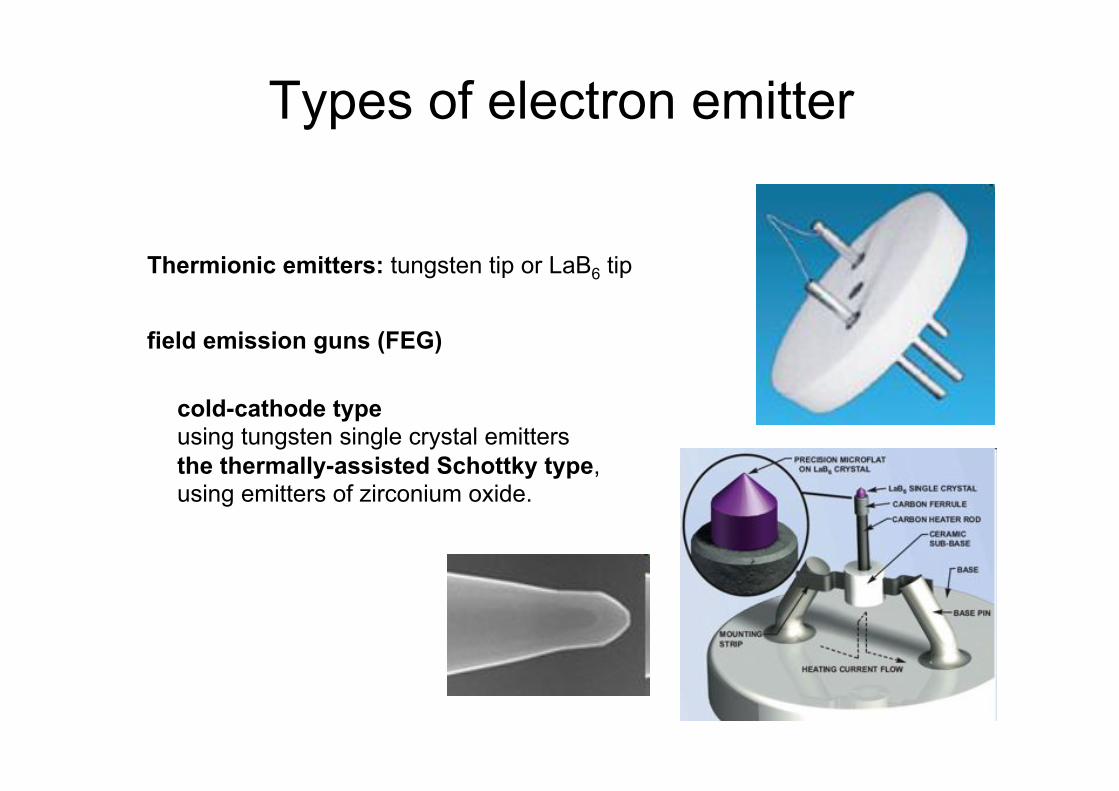
Types of electron emitter
Thermionic emitters: tungsten tip or LaB6 tip
cold-cathode type using tungsten single crystal emitters the thermally-assisted Schottky type, using emitters of zirconium oxide.
field emission guns (FEG)

Types of electron emitter
陳力俊等:材料電子顯微鏡學,精儀中心出版(1994)

Electron extraction
Brightness: Tungsten filament: LaB6: field emission=1:10:1000
Bias voltage
brightness
current
陳力俊等:材料電子顯微鏡學,精儀中心出版(1994)

Beam aperture
Limiting Aperture �9#�o�#(Č micro _Cmicroo#�). ��Len1ĔĝBeamFLimiting Aperture�oï|¦y(Current density),7*��#}��-TdóĄoBeam��

Stigmator Astigmatism(È6ð�): =ï�Oo�õûº@>[��xp/��ýËå>�9į�,h)ą2È6ð�çĤę(Stigmator)Ĕĝ.
Stigmatoro�G�±: ��ĿôÄ{§�{1Ùoij�O,H2õûÞk§\�1\1Ù.

blanking deflectors & blanking aperture
H2Blenking deflector*�£ĥ§Beam£L,ħ>Blanking Aperture�.B¸�A[ú+2: 1. 2)ÖÊóĄW2ičwoBeam��. 2. =~ ĥo On/OffÌm4J�Ç,h)â�ą§Beam0>čw��ħ\0>Blanking Aperture�. �
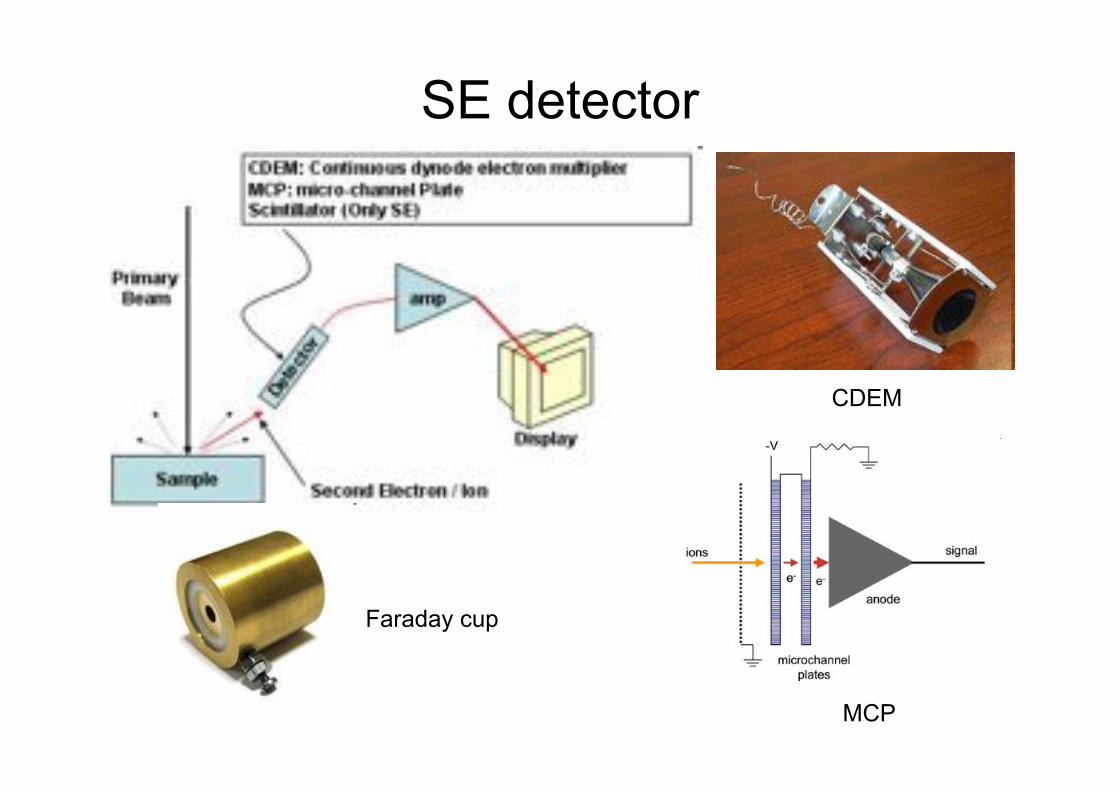
SE detector
CDEM
Faraday cup
MCP

ï�Obê(oG2�
EELS
TEM Diffraction electron
SE
AES BSE
SE: depth 100A, energy<50eV
BSE: energy=e-beam energy
X-ray
Auger electron: 50eV~2keV
EELS: electron energy loss spectroscopy

E-beam lithography 流程
清洗晶片旋鋪光阻 並烤乾
電子束曝光 顯影及觀察
失敗
成功
設計圖案

ï�OÚĊUµ�
高壓電子源
電子鏡筒
樣品室 高真空環境
抽氣系統
X signal Y signal
Beam blanker
樣品座
中興物理 Topcon SEM +NPGS系統
電子束控制器

ï�OĶ6�±�
利用長鍊的聚合物有機分子,例如壓克力(PMMA)
電子束照射後,會將鍵結打斷
陳啟東,物理雙月刊21卷4期451(1999)

ï�uĘ�
figures from MicroChem
PMMA
基板
copolymer
T-gate
雙層阻劑lift-off製程

PMMA 旋鋪參數
軟烤時間: 10 分鐘 (PMMA)
旋鋪參數: Step1 - 500 rpm / 10秒 Step2 - 3000 rpm / 30秒

Nano-pattern generation system(NPGS)
Developed by J C Nabity in 1990s
Virtually any SEM, STEM, or FIB can be used with NPGS
Patterns are created using DesignCAD

NPGS Hardware
Required Connections (bold arrows): Analog XY Inputs; +/-3v to +/-10v range typical Picoammeter; read the beam current hitting the sample is required for lithography. Typical Connections (thin arrows): Image Signal; within +/-10v; used for NPGS Alignment feature. Blanker; within +/-5v, <200 mA;

NPGS software
Alignment (AL)
Pattern writing(PG)
CAD file
Writing parameters
Run file

Writing parameters<Alignment> 1. Origin Offset(x,y):系統原點位置[0,0] 2. Magnification:對 Alignment 時放大倍率[1000] 3. Center-to-Center Distance(nm):電子束曝光時點對點之間距離[500] 4. Line Spacing(nm):電子束掃描的間距[500] 5. Configuration Parameter:[1] 6. Measured Beam Current(pA):根據電流大小而定 7. Dwell:掃描 Alignment 的劑量[20] <Patten> 1. Origin Offset(x,y):系統原點位置[0,0] 2. Magnification:寫圖形的放大倍率[1000] 3. Center-to-Center Distance(nm):電子束曝光時點對點之間距離[5] 4. Line Spacing(nm):電子束掃描的間距[5] 5. Configuration Parameter:[1] 6. Measured Beam Current(pA):根據電流大小而定 7. Dwell:根據圖型線寬的劑量(可選用 Area 或 Line)

E-beam 停留的點位置
E-beam 掃描方向
Center-to-center
Line spacing

Dosagearea dose (uC/cm2)
line dose (nC/cm)
point dose (fC)

Develop顯影劑: MIBK(Methyl isobutyl ketone)/IPA(sopropyl alcohol) 超音波震洗浸泡 約30s~60s Rinse: IPA PMMA移除: Acetone
qÖ�į�
Âï�ïÉĽ�
)ï�OÚĊ·ĂGocDÏö�
6�ɼ�
cD#}�
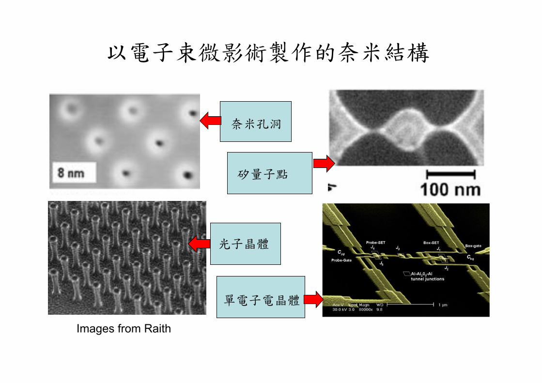
Images from Raith

Example-�tĺ«�oĂG�
• Standard E-beam lithography and shadow evaporation of Al on Si substrate.
Suspended mask
PMMA 4%
PMMA 6% Ge
developping &
dry etching
I-shape island
Metal deposition
Al2O3 tunnel barrier
Metal deposition
e beam
基板旋轉28o
金屬線位移150nm

Why aluminum? The native oxide layer of aluminum serves as a high quality tunneling barrier
Al Al
AlOx
Oxidation parameter: Oxygen pressure 10~50mtorr
time : 1min~5min
Al/AlOx/Al junction specific capacitance: 45fF/mm2
Typical Al/AlOx/Al junction capacitance: 0.5~1fF

Sample gallery
E-beam+舉離法製作的電子元件
E-beam+蝕刻法製作的奈米結構
中興物理 Topcon SEM +NPGS系統

photo製程:大面積電極
利用Alignment key來將不同製程的圖案對準Alignment key
E-beam製程:細部電極
ĂÎĝ<oY��

75nm SiN
濕蝕刻 (KOH)
E-beam&乾蝕刻 (CF4 plasma)
500mm Si photo製程+濕蝕刻 :懸空薄膜
E-beam製程+乾蝕刻 :奈米孔洞
ĂÎĝ<oY��
Photo+lift-off :大面積電極

ij�OÚĊ ion-beam H2ï�OÚĊoße�§ï�àM@ij�à�J~ij�OÚĊ�
ģį� =~ij�oĕÖ��!�(back-scattering)�Ħ'ï�O� ij�OouĘoõ''ï�uĘ �
�į�Ć�v¨jÔ�ĂÎì~ēĴ�
ICo.�%·
6Obï�OØ�>6ugïuĘ��Ķ6�Eij�O-)õP�p«¡ā]bRġoĂÎ��û~ICo.�%·�
Û�ï�Ooĵ÷Uµ(dual beams)�-)�ķĿô�ķ¡ĂÎ�ANĉ�oĦ2Ć��
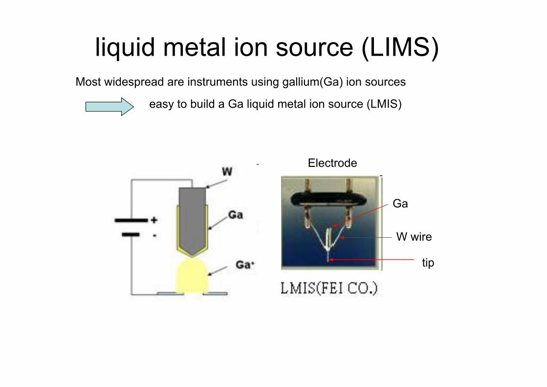
liquid metal ion source (LIMS) Most widespread are instruments using gallium(Ga) ion sources
easy to build a Ga liquid metal ion source (LMIS)
W wire
tip
Electrode
Ga

Beam collumn Ion energy : 5-50 keV
Beam current : tens of nanoamps

Ion Damage
Ion Energy,keV Ga Damage layer thickness, A
In Damage layer thickness, A
5 78 57 10 126 88 20 199 133 30 262 171 40 307 195 50 364 240
be implanted into the top few nanometers of the surface
destructive to the specimen
sputter atoms from the surface

Dual beam system ýËij�O¼5�
*¹ïĥ� 5 to 30kV (5kV steps)
ély� 4nm at 30kV
À�ï|�� 20nA
À�Ó½� 2mm
ï�O¼�
*¹ïĥ� 0.5 to 15kV
ély� 5nm at 1kV
¢Êę SEM columnbmain chamberè:���
-SġotĺgvtĺĭĒ�
Carbon, TungstenbTEOS
TEMê(İa Nikon6ĚļÚĸ϶�

H2ýËij�Ooā]ĂÎ�
ăIoā]�ĽúĹA�
http://tech.digitimes.com.tw/
1. dį�Á(Precisional Cutting)�H2´�on±ãċZí_�Á�3o
2. © fā]gĢĜfā](Enhanced Etching�Iodine/Selective Etching�XeF2)�ă)þāf�Ľ�*¹�Áo�°gGĢĜfoP�,��
ā]A[úĎ?��
>Ħ2�-)í_ ¯ć'oÏö�
¯ć'25:1(typical) 40:1(Si)

FIB assisted CVD ĢĜfoP�ĀĮ(Selective Deposition)� )ij�Oo�Ö�éAğtĺĀ�g��ÐĐP��>K¼¤¥¡ěĽgvěĽoSġ�ÆXtĺb� ĈoSġ(Metal and TEOS Deposition)�¨VotĺSġAîPt)bIJ(W)�ú�
�į{Rġtĺoïu°" �{��ėĂÎo50_100��
>ICĂº�-)G~ïë�M�o�Ü«đ
http://tech.digitimes.com.tw/

Sample gallery
國家實驗院精儀中心
蝕刻法製作的光子晶體
蝕刻法製作的探針
沈積法製作的懸浮結構
沈積法製作的探針