ee5970 computer engineering seminar spring 2012 michigan technological university based on: a...
TRANSCRIPT

EE5970 Computer Engineering SeminarSpring 2012
Michigan Technological University
Based on:A Low-Power FPGA Based on Autonomous
Fine-Grain Power GatingShota Ishihara, Masanori Hariyama, and Michitaka Kameyama
Rohit A. Bhatia
IEEE TRANSACTIONS ON VERY LARGE SCALE INTEGRATION (VLSI) SYSTEMS. VOL. 19, NO. 8, AUGUST 2011

Contents
• About FPGAs• Fine-Grain Power Gating and Related Work
– Asynchronous FPGAs– Wave-Pipelining for Bit-Serial FPGAs– Sleep Signal Generation Techniques for Power Gating
• Architecture of the proposed FPGA– Overview– Fundamental Principle of Autonomous Fine-Grain Power Gating
• Circuit Implementation• Evaluation
2

Field Programmable Gate Array (FPGA)
• FPGAs offer greater flexibility than ASICs (Application Specific Integrated Circuits) in terms of usability
• Used in various products:– Programmable Logic Controllers (PLCs)– Medical Instruments– Gigabit Ethernet Controllers– Wireless devices
• End user can program as per the requirement, enabling incredible customization to the application
XILINX FPGA in useSource
3
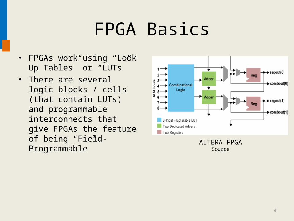
• FPGAs work using “Look Up Tables” or “LUTs”
• There are several logic blocks / cells (that contain LUTs) and programmable interconnects that give FPGAs the feature of being “Field-Programmable”
4
FPGA Basics
ALTERA FPGASource

• About FPGAs• Fine-Grain Power Gating and Related Work
– FPGA Power Considerations and LEDR– Wave-Pipelining for Bit-Serial FPGAs– Sleep Signal Generation Techniques for Power Gating
• Architecture of the proposed FPGA– Overview– Fundamental Principle of Autonomous Fine-Grain Power Gating
• Circuit Implementation• Evaluation
5

Power Gating• Certain logic blocks can be
switched-off when not in use to minimize power consumption– Power consumed by sleep
controller must be less than that saved by switching off the block
• Power Gating:– Fine-Grain: Each LUT has its
own sleep transistor and sleep controller
– Coarse-Grain: A large number of LUTs share a single sleep controller
6
Overall Architecture [1]

• Fine-Grain: Lower standby power but greater dynamic power (sleep transistors)
• Coarse-Grain: Lower dynamic power but higher standby power (active blocks)
7
Overall Architecture [1]
Power Considerations

LEDR (Level Encoded Dual-Rail)• Dual-rail code provides scope for
data transmission and its validity• Two wires per bit are used• LEDR or Level Encoded Dual-Rail
based architecture achieves lowest dynamic power consumption among all dual-rail architectures considered
• Decision to shut down and wake up the power-gated domain is based on its activity
• No spacer required: less transitions, more throughput and less power consumption
8
Dual-Rail code
Dual-rail code Interpretation
00 “reset” value
01 0 value
10 1 value
11 unused
[2]
[3]

Wave-Pipelining for Bit-Serial FPGAs
• Allow circuit to process new data set before the previous data set reached the registers.
• Used to achieve small area without performance degradation – not to reduce standby power
9

Sleep Signal Generation Techniques for Power Gating
• Software Based – Can be used, but suffers from large power and delay overheads– Overheads make this technique not suitable for fine-grain power gating
• Hardware Based – A power-gated domain is shut down after it stays idle for a given
threshold– Static Sleep Signal Generator (SSSG) – predefined threshold time– Dynamic Sleep Signal Generator (DSSG) – variable threshold time– Both, SSSG and DSSG use instruction level analysis of the activity of the
power-gated domains – applicable only to block-level power gating
10
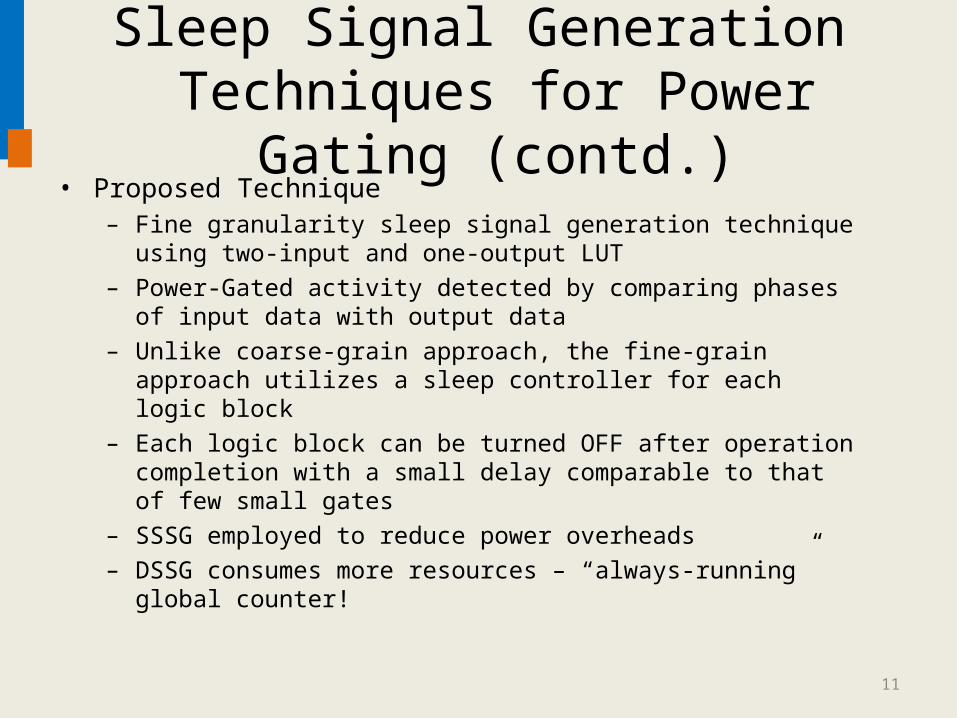
Sleep Signal Generation Techniques for Power Gating (contd.)
• Proposed Technique– Fine granularity sleep signal generation technique using two-input and
one-output LUT– Power-Gated activity detected by comparing phases of input data with
output data– Unlike coarse-grain approach, the fine-grain approach utilizes a sleep
controller for each logic block– Each logic block can be turned OFF after operation completion with a
small delay comparable to that of few small gates– SSSG employed to reduce power overheads– DSSG consumes more resources – “always-running” global counter!
11

12
• About FPGAs• Fine-Grain Power Gating and Related Work
– FPGA Power Considerations and LEDR– Wave-Pipelining for Bit-Serial FPGAs– Sleep Signal Generation Techniques for Power Gating
• Architecture of the proposed FPGA– Overview– Fundamental Principle of Autonomous Fine-Grain Power Gating
• Circuit Implementation• Evaluation
Architecture of the proposed FPGAOverview
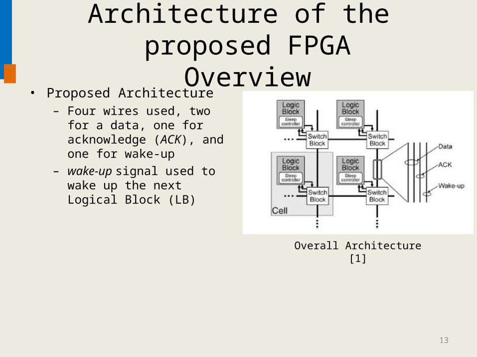
• Proposed Architecture– Four wires used, two for a data,
one for acknowledge (ACK), and one for wake-up
– wake-up signal used to wake up the next Logical Block (LB)
13
Overall Architecture [1]

Architecture of the proposed FPGAOverview (contd.)
• Cell Structure– Four wires used, two for a data,
one for acknowledge (ACK), and one for wake-up
– Four pass switches and a memory bit make a pass-switch block
14
Cell Structure [4]

Architecture of the proposed FPGAOverview (contd.)
• Direct Allocation of a Control/Data Flow Graph (CDFG) mapping used• Operations mapped onto the LBs• Input of a logic block is directly connected to the output of another logic
block• Reduction in the complexity of the interconnection network between LBs!
15
Direct Allocation [5]
Operation
Data Dependency

Fundamental Principle of Autonomous Fine-Grain Power Gating
• On arrival of new data on an LB, the phase of the input data is different from that of the output data
• On completion of operation, the phase of the input data and output data are the same
• Proposed sleep controller extracts and compares the phases of input and output data.
16
Activity detection using the asynchronous architecture [6]
0 0
1 0
1 1
0 1
0 0

Fundamental Principle of Autonomous Fine-Grain Power Gating (contd.)
• On same phase of input and output data, comparator output is 0 and 1 otherwise
• Problems:– Sleep Transistor takes
time to switch ON on the arrival of new data
– Switching power could be more than the “saved” power
17
Phase extraction and wake-up signal generation [7]

Fundamental Principle of Autonomous Fine-Grain Power Gating (contd.)
• Problems can be solved by introducing a standby state:1. wake up the LB before the
data arrives;2. power OFF the LB only when
the data does not come for quite a while (threshold time)
18
Sleep control strategy [8]

Fundamental Principle of Autonomous Fine-Grain Power Gating (contd.)
19Illustration of the proposed power gating method [9]

20
• About FPGAs• Fine-Grain Power Gating and Related Work
– FPGA Power Considerations and LEDR– Wave-Pipelining for Bit-Serial FPGAs– Sleep Signal Generation Techniques for Power Gating
• Architecture of the proposed FPGA– Overview– Fundamental Principle of Autonomous Fine-Grain Power Gating
• Circuit Implementation• Evaluation

Circuit Implementation
21
Block diagram of a LB [10]
• The wake-up signal is used to wake up the LB before new data arrives
• Latches retain the wake-up signal until all the input data arrive
• Programmable delay is used to delay the sleep signal based on the set threshold time
Circuit Implementation (contd.)
22
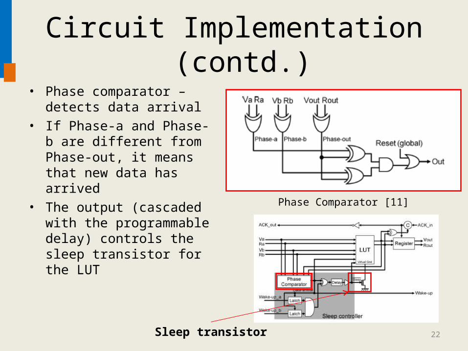
Phase Comparator [11]
• Phase comparator – detects data arrival
• If Phase-a and Phase-b are different from Phase-out, it means that new data has arrived
• The output (cascaded with the programmable delay) controls the sleep transistor for the LUT
Sleep transistor

Circuit Implementation (contd.)
23
Multiplexer Based LUT for LEDR encoding [12]
• Problem comes with invalid inputs – large number of multiplexers is required to keep the previous output

Circuit Implementation (contd.)
24
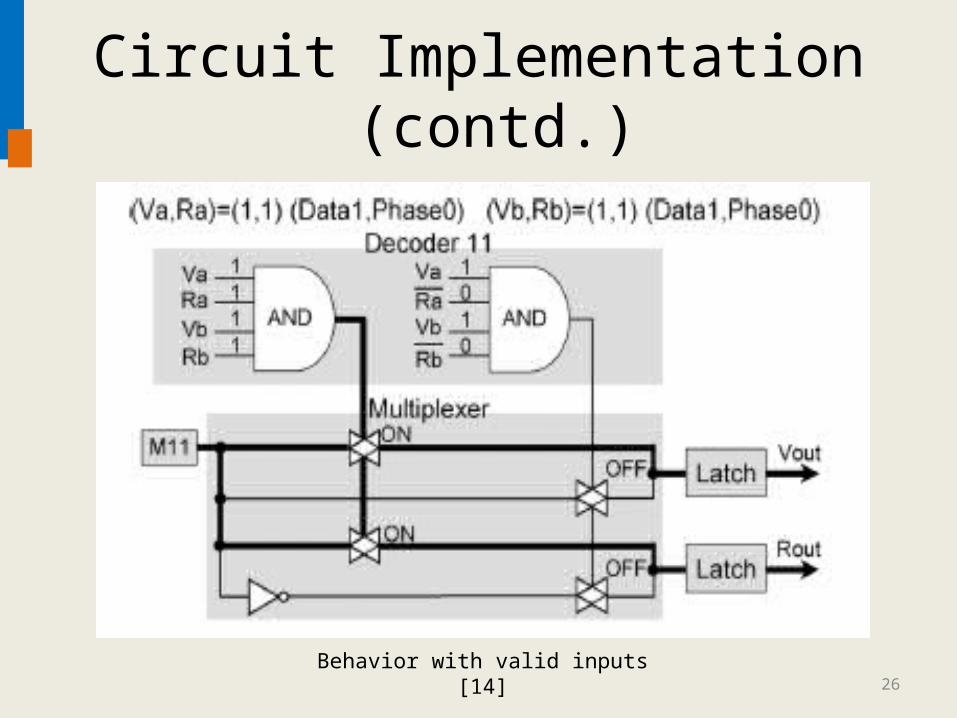
Block diagram of the proposed LUT [13]
• Decoders exclude invalid data patterns (ones with different phases)
• Number of transistors is reduced since invalid inputs aren’t fed to the multiplexer stage

Circuit Implementation (contd.)
25Behavior with invalid inputs [14]
Circuit Implementation (contd.)
26Behavior with valid inputs [14]

27
• About FPGAs• Fine-Grain Power Gating and Related Work
– FPGA Power Considerations and LEDR– Wave-Pipelining for Bit-Serial FPGAs– Sleep Signal Generation Techniques for Power Gating
• Architecture of the proposed FPGA– Overview– Fundamental Principle of Autonomous Fine-Grain Power Gating
• Circuit Implementation• Evaluation

Evaluation
28
• The following results come from HSPICE simulation at 85°C:– Proposed FPGA when compared to conventional LEDR-based FPGA:
1. Standby power of the cell is reduced by 69% in the sleep state2. The area and dynamic power of the logic block are increased by 14% and
6%, respectively– Proposed FPGA when compared to synchronous FPGA:
1. Standby power of the cell is reduced by 38% in the sleep state and delay is increased by 34%
2. The area is increased by 170% causing a reduction in available logic by 63% for the same given area

Evaluation (contd.)
29
• The concepts demonstrated for a simple data path for a small LUT size can be applied to the complex data path architectures of modern FPGAs
• The power and area of the sleep controller are much smaller than those of the data path components such as a logic block and a switch block. In a more complex data path architecture, the overheads of the sleep controller are smaller.

Thank you for your time!Questions?
30

Image sources[1] Shota Ishihara, Masanori Hariyama, and Michitaka Kameyama. (2011, Aug.). “A Low-Power FPGA Based on AutonomousFine-Grain Power Gating” IEEE TRANSACTIONS ON VERY LARGE SCALE INTEGRATION (VLSI) SYSTEMS. [On-line]. 19(8), pp. 1397, Fig. 3 Available: http://ieeexplore.ieee.org/xpls/abs_all.jsp?arnumber=5483137 [Feb. 12, 2012][2] Shota Ishihara, Masanori Hariyama, and Michitaka Kameyama. (2011, Aug.). “A Low-Power FPGA Based on AutonomousFine-Grain Power Gating” IEEE TRANSACTIONS ON VERY LARGE SCALE INTEGRATION (VLSI) SYSTEMS. [On-line]. 19(8), pp. 1395, Fig. 1 Available: http://ieeexplore.ieee.org/xpls/abs_all.jsp?arnumber=5483137 [Feb. 12, 2012][3] Shota Ishihara, Masanori Hariyama, and Michitaka Kameyama. (2011, Aug.). “A Low-Power FPGA Based on AutonomousFine-Grain Power Gating” IEEE TRANSACTIONS ON VERY LARGE SCALE INTEGRATION (VLSI) SYSTEMS. [On-line]. 19(8), pp. 1395, Fig. 2 Available: http://ieeexplore.ieee.org/xpls/abs_all.jsp?arnumber=5483137 [Feb. 13, 2012][4] Shota Ishihara, Masanori Hariyama, and Michitaka Kameyama. (2011, Aug.). “A Low-Power FPGA Based on AutonomousFine-Grain Power Gating” IEEE TRANSACTIONS ON VERY LARGE SCALE INTEGRATION (VLSI) SYSTEMS. [On-line]. 19(8), pp. 1397, Fig. 4 Available: http://ieeexplore.ieee.org/xpls/abs_all.jsp?arnumber=5483137 [Feb. 13, 2012][5] Shota Ishihara, Masanori Hariyama, and Michitaka Kameyama. (2011, Aug.). “A Low-Power FPGA Based on AutonomousFine-Grain Power Gating” IEEE TRANSACTIONS ON VERY LARGE SCALE INTEGRATION (VLSI) SYSTEMS. [On-line]. 19(8), pp. 1397, Fig. 5 Available: http://ieeexplore.ieee.org/xpls/abs_all.jsp?arnumber=5483137 [Feb. 14, 2012][6] Shota Ishihara, Masanori Hariyama, and Michitaka Kameyama. (2011, Aug.). “A Low-Power FPGA Based on AutonomousFine-Grain Power Gating” IEEE TRANSACTIONS ON VERY LARGE SCALE INTEGRATION (VLSI) SYSTEMS. [On-line]. 19(8), pp. 1397, Fig. 6 Available: http://ieeexplore.ieee.org/xpls/abs_all.jsp?arnumber=5483137 [Feb. 14, 2012][7] Shota Ishihara, Masanori Hariyama, and Michitaka Kameyama. (2011, Aug.). “A Low-Power FPGA Based on AutonomousFine-Grain Power Gating” IEEE TRANSACTIONS ON VERY LARGE SCALE INTEGRATION (VLSI) SYSTEMS. [On-line]. 19(8), pp. 1398, Fig. 7 Available: http://ieeexplore.ieee.org/xpls/abs_all.jsp?arnumber=5483137 [Feb. 14, 2012][8] Shota Ishihara, Masanori Hariyama, and Michitaka Kameyama. (2011, Aug.). “A Low-Power FPGA Based on AutonomousFine-Grain Power Gating” IEEE TRANSACTIONS ON VERY LARGE SCALE INTEGRATION (VLSI) SYSTEMS. [On-line]. 19(8), pp. 1398, Fig. 9 Available: http://ieeexplore.ieee.org/xpls/abs_all.jsp?arnumber=5483137 [Feb. 14, 2012]
31

[9] Shota Ishihara, Masanori Hariyama, and Michitaka Kameyama. (2011, Aug.). “A Low-Power FPGA Based on AutonomousFine-Grain Power Gating” IEEE TRANSACTIONS ON VERY LARGE SCALE INTEGRATION (VLSI) SYSTEMS. [On-line]. 19(8), pp. 1398, Fig. 10 Available: http://ieeexplore.ieee.org/xpls/abs_all.jsp?arnumber=5483137 [Feb. 15, 2012][10] Shota Ishihara, Masanori Hariyama, and Michitaka Kameyama. (2011, Aug.). “A Low-Power FPGA Based on AutonomousFine-Grain Power Gating” IEEE TRANSACTIONS ON VERY LARGE SCALE INTEGRATION (VLSI) SYSTEMS. [On-line]. 19(8), pp. 1399, Fig. 12 Available: http://ieeexplore.ieee.org/xpls/abs_all.jsp?arnumber=5483137 [Feb. 15, 2012][11] Shota Ishihara, Masanori Hariyama, and Michitaka Kameyama. (2011, Aug.). “A Low-Power FPGA Based on AutonomousFine-Grain Power Gating” IEEE TRANSACTIONS ON VERY LARGE SCALE INTEGRATION (VLSI) SYSTEMS. [On-line]. 19(8), pp. 1399, Fig. 13 Available: http://ieeexplore.ieee.org/xpls/abs_all.jsp?arnumber=5483137 [Feb. 15, 2012][12] Shota Ishihara, Masanori Hariyama, and Michitaka Kameyama. (2011, Aug.). “A Low-Power FPGA Based on AutonomousFine-Grain Power Gating” IEEE TRANSACTIONS ON VERY LARGE SCALE INTEGRATION (VLSI) SYSTEMS. [On-line]. 19(8), pp. 1400, Fig. 15 Available: http://ieeexplore.ieee.org/xpls/abs_all.jsp?arnumber=5483137 [Feb. 15, 2012][13] Shota Ishihara, Masanori Hariyama, and Michitaka Kameyama. (2011, Aug.). “A Low-Power FPGA Based on AutonomousFine-Grain Power Gating” IEEE TRANSACTIONS ON VERY LARGE SCALE INTEGRATION (VLSI) SYSTEMS. [On-line]. 19(8), pp. 1400, Fig. 16 Available: http://ieeexplore.ieee.org/xpls/abs_all.jsp?arnumber=5483137 [Feb. 15, 2012][14] Shota Ishihara, Masanori Hariyama, and Michitaka Kameyama. (2011, Aug.). “A Low-Power FPGA Based on AutonomousFine-Grain Power Gating” IEEE TRANSACTIONS ON VERY LARGE SCALE INTEGRATION (VLSI) SYSTEMS. [On-line]. 19(8), pp. 1400, Fig. 17 Available: http://ieeexplore.ieee.org/xpls/abs_all.jsp?arnumber=5483137 [Feb. 15, 2012][15] Shota Ishihara, Masanori Hariyama, and Michitaka Kameyama. (2011, Aug.). “A Low-Power FPGA Based on AutonomousFine-Grain Power Gating” IEEE TRANSACTIONS ON VERY LARGE SCALE INTEGRATION (VLSI) SYSTEMS. [On-line]. 19(8), pp. 1400, Fig. 18 Available: http://ieeexplore.ieee.org/xpls/abs_all.jsp?arnumber=5483137 [Feb. 15, 2012]
32