embedded systems design using microcontroller msp430 · embedded systems design using...
TRANSCRIPT

1
Embedded Systems Design Using Microcontroller MSP430
Ts. Lê Mạnh HảiKhoa CNTT,
ĐH Kỹ thuật Công nghệ TP HCM
2
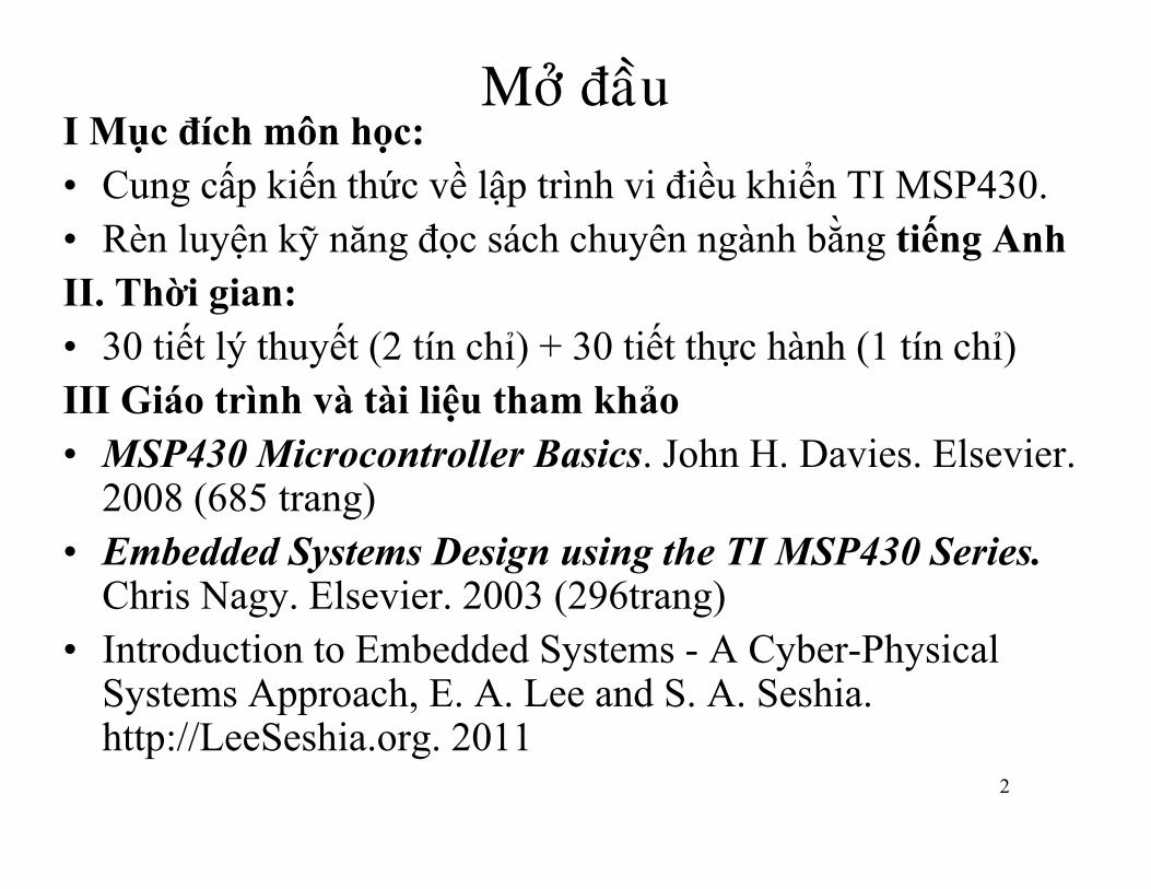
Môû ñaàuI Mục đích môn học:• Cung cấp kiến thức về lập trình vi điều khiển TI MSP430. • Rèn luyện kỹ năng đọc sách chuyên ngành bằng tiếng AnhII. Thời gian:• 30 tiết lý thuyết (2 tín chỉ) + 30 tiết thực hành (1 tín chỉ)III Giáo trình và tài liệu tham khảo• MSP430 Microcontroller Basics. John H. Davies. Elsevier.
2008 (685 trang)• Embedded Systems Design using the TI MSP430 Series.
Chris Nagy. Elsevier. 2003 (296trang)• Introduction to Embedded Systems - A Cyber-Physical
Systems Approach, E. A. Lee and S. A. Seshia. http://LeeSeshia.org. 2011
3

4
IV. Đánh giá:• Thi kết thúc môn: Bài tự luận với 3 câu hỏi. V. Giáo viên:• Ts. Lê Mạnh Hải. Tel: 0985399000. • Không gọi điện thoại để hỏi hay xin điểm,
email: [email protected], [email protected]
• Website: giangvien.hutech.edu.vn• GV thực hành: Nguyễn Ngọc Đức.
0978629557
5
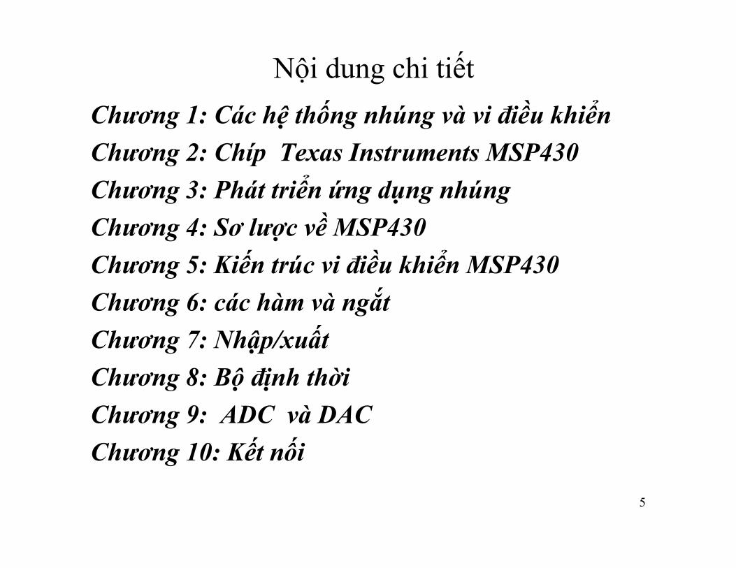
Nội dung chi tiết Chương 1: Các hệ thống nhúng và vi điều khiểnChương 2: Chíp Texas Instruments MSP430 Chương 3: Phát triển ứng dụng nhúngChương 4: Sơ lược về MSP430Chương 5: Kiến trúc vi điều khiển MSP430Chương 6: các hàm và ngắtChương 7: Nhập/xuấtChương 8: Bộ định thờiChương 9: ADC và DACChương 10: Kết nối
6
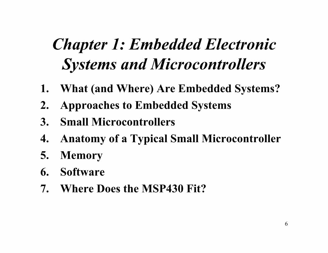
Chapter 1: Embedded Electronic Systems and Microcontrollers
1. What (and Where) Are Embedded Systems?2. Approaches to Embedded Systems3. Small Microcontrollers4. Anatomy of a Typical Small Microcontroller5. Memory6. Software7. Where Does the MSP430 Fit?
7
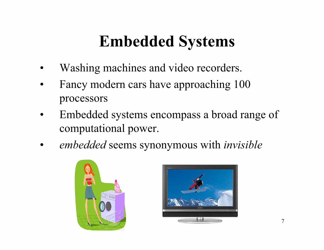
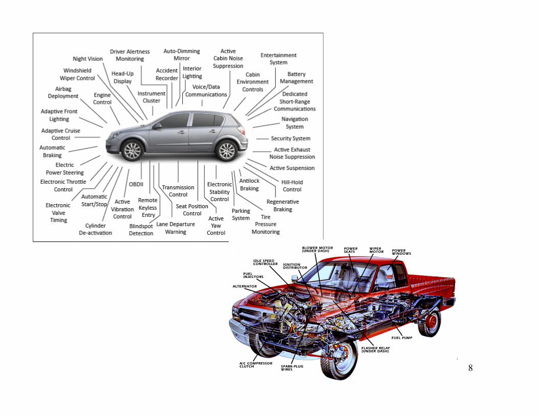
Embedded Systems• Washing machines and video recorders. • Fancy modern cars have approaching 100
processors• Embedded systems encompass a broad range of
computational power.• embedded seems synonymous with invisible
8
9
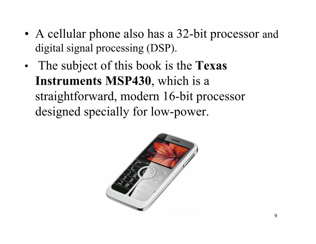
• A cellular phone also has a 32-bit processor and digital signal processing (DSP).
• The subject of this book is the Texas Instruments MSP430, which is a straightforward, modern 16-bit processor designed specially for low-power.
10
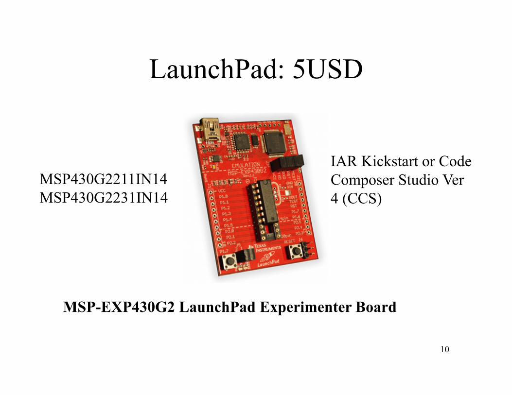
LaunchPad: 5USD
MSP-EXP430G2 LaunchPad Experimenter Board
MSP430G2211IN14 MSP430G2231IN14
IAR Kickstart or Code Composer Studio Ver 4 (CCS)
11
Many different approaches can be taken for the design of embedded systems
• The general trend is toward digital systems and increasing integration: Systems that used analog electronics or small-scale integrated circuits (ICs) in the past
• Now more likely to use larger digital ICs
12
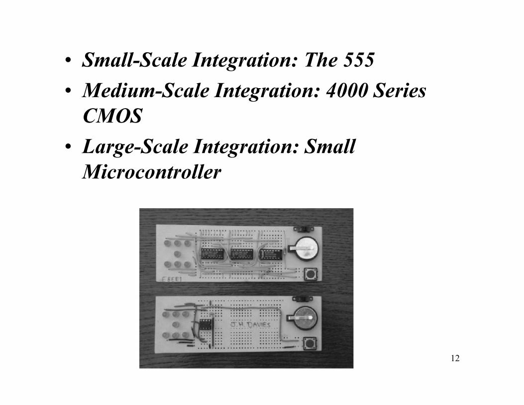
• Small-Scale Integration: The 555 • Medium-Scale Integration: 4000 Series
CMOS• Large-Scale Integration: Small
Microcontroller
13
Larger Systems• Application-specific integrated circuits (ASICs)
– Specially designed for a particular application• Field-programmable gate arrays (FPGAs) and
programmable logic devices (PLDs)– Essentially an array of gates and flip-flops,
which can be connected by programming the device to produce the desired function
• Microcontrollers– These have nearly fixed hardware built around a
central processing unit (CPU)
14
Small Microcontrollers• Microprocessor or microcontroller?• Process 8 or 16 bits of data and have a 16-bit
address bus• 64KB of memory• Main function is likely to be sequential control
rather than computation.
15
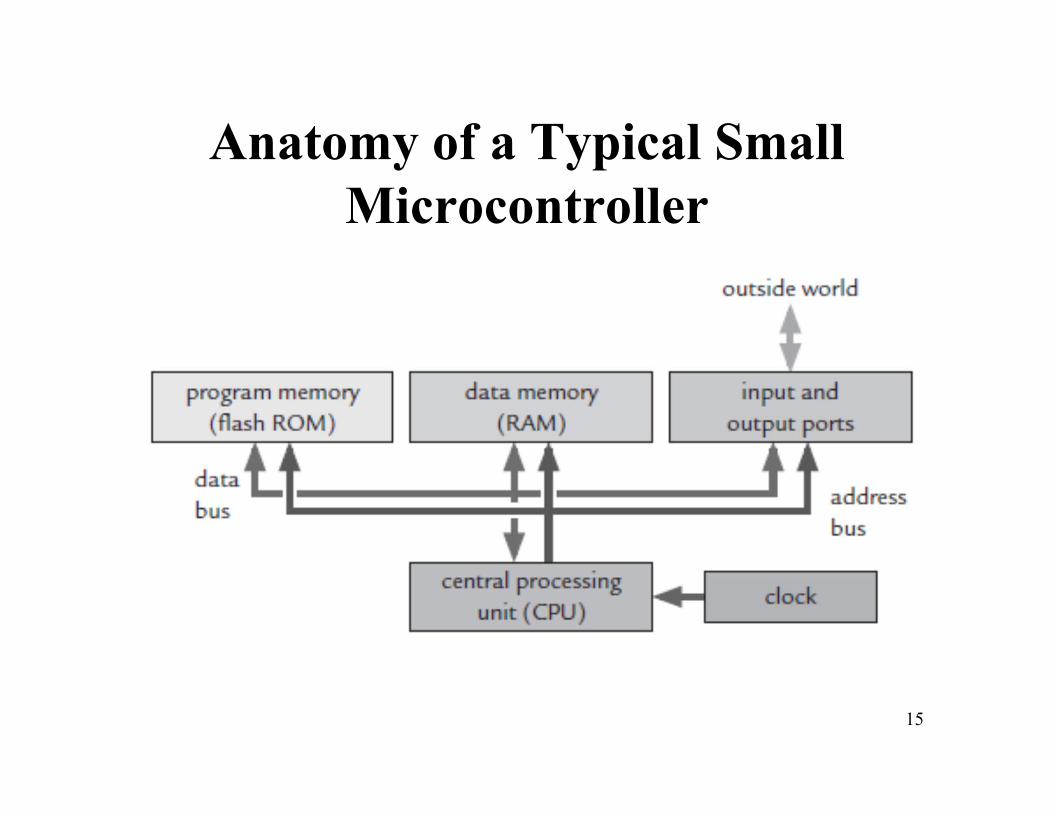
Anatomy of a Typical Small Microcontroller

16
• Central processing unit– Arithmetic logic unit (ALU), which performs
computation.– Registers needed for the basic operation of the
CPU, such as the program counter (PC), stack pointer (SP), and status register (SR).
– Further registers to hold temporary results.– Instruction decoder and other logic to control
the CPU, handle resets, and interrupts, and so on.
17
• Memory for the program: Nonvolatile (read-only memory, ROM), meaning that it retains its contents when power is removed.
• Memory for data: Known as random-access memory (RAM) and usually volatile.
• Input and output ports: To provide digital communication with the outside world.
• Address and data buses: To link these subsystems to transfer data and instructions.
• Clock: To keep the whole system synchronized.
18
Timers: Most microcontrollers have at least one timer because of the wide range of functions that they provide.
Watchdog timer: This is a safety feature, which resets the processor if the program becomes stuck in an infinite loop.
Communication interfaces: A wide choice of interfaces is available to exchange information with another IC or system.
Nonvolatile memory for data: This is used to store data whose value must be retained when power is removed.
Analog-to-digital converter: This is very common because so many quantities in the real world vary continuously.
Digital-to-analog converter: This is much less common, because most analog outputs can be simulated using PWM.
Real-time clock: These are needed in applications that must track the time of day.
Monitor, background debugger, and embedded emulator: These are used to download the program into the MCU
19
Memory
• Each location can typically store 1 byte (8 bits or 1B) of data and is often called a register
• Memory is linked to the CPU by buses for data, address, and control
20
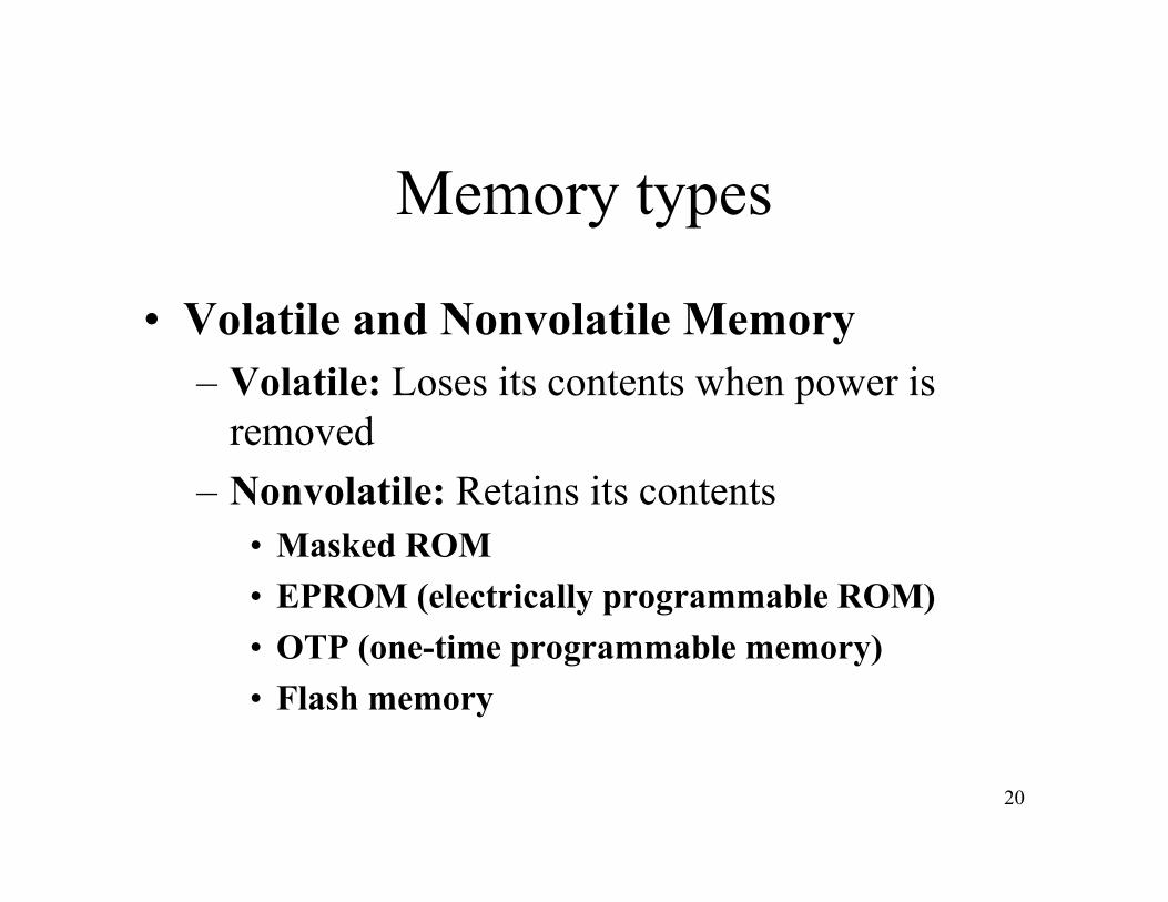
Memory types
• Volatile and Nonvolatile Memory– Volatile: Loses its contents when power is
removed– Nonvolatile: Retains its contents
• Masked ROM• EPROM (electrically programmable ROM)• OTP (one-time programmable memory)• Flash memory
21
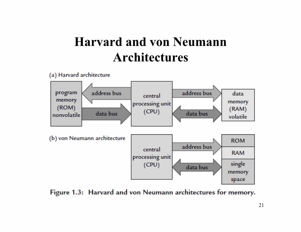
Harvard and von Neumann Architectures
22
Software
• C: The most common choice for small microcontrollers nowadays. A compiler translates C into machine code that the CPU can process.
• IAR and CCS
23
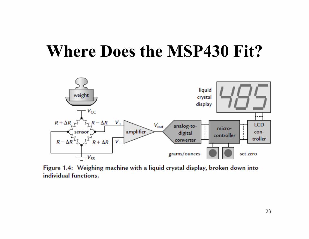
Where Does the MSP430 Fit?
24
Quizzes
• Name some embedded systems?• What is microcontroller?• What are differences between Harvard and
von Neumann Architectures?
25
What is next?
• CHAPTER 2: The Texas Instruments MSP430 (Page 21-42)

26
Chíp Texas Instruments MSP430
27
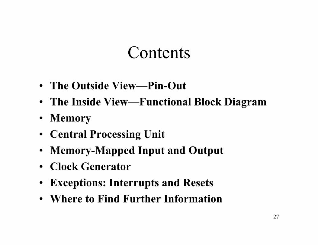
Contents
• The Outside View—Pin-Out• The Inside View—Functional Block Diagram• Memory• Central Processing Unit• Memory-Mapped Input and Output• Clock Generator• Exceptions: Interrupts and Resets• Where to Find Further Information

28
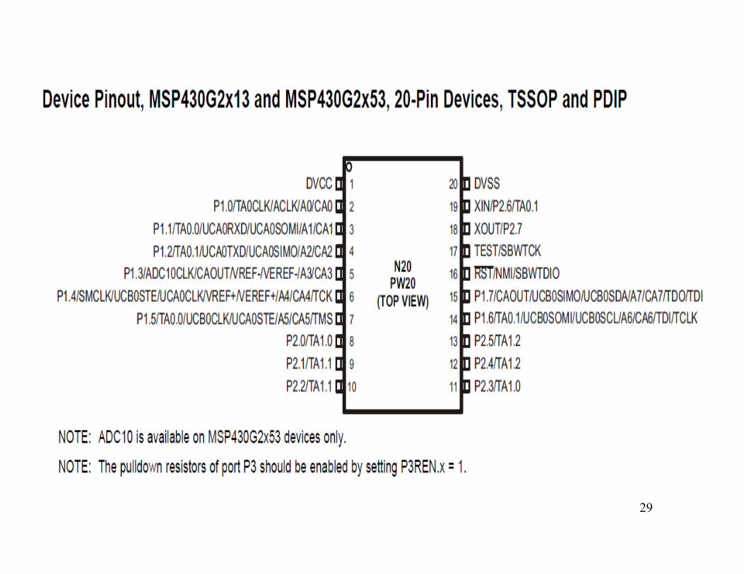
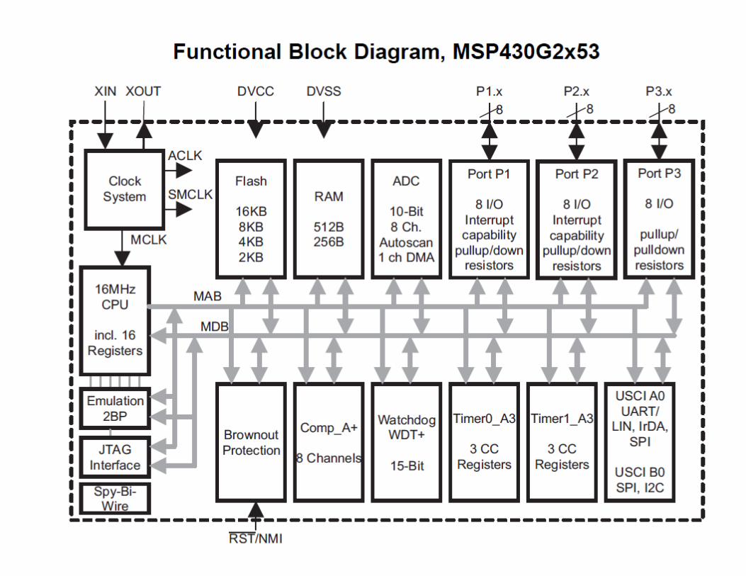
The Outside View—Pin-Out
• pin-out: 14-pin plastic dual-in-line package (PDIP)
• Perhaps the most obvious feature is that almost all pins have several functions
• Most applications do not use all the peripherals so, with luck, there is no conflict where a design needs more than one function on a pin simultaneously
29

30
31
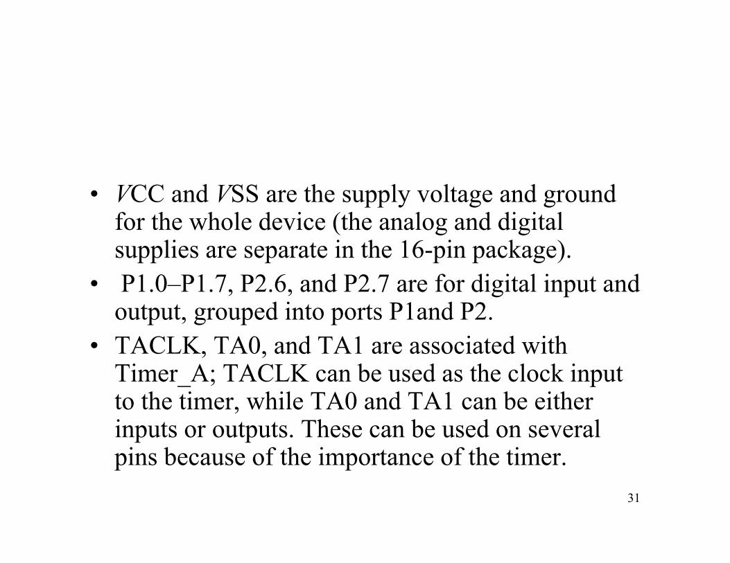
• VCC and VSS are the supply voltage and ground for the whole device (the analog and digital supplies are separate in the 16-pin package).
• P1.0–P1.7, P2.6, and P2.7 are for digital input and output, grouped into ports P1and P2.
• TACLK, TA0, and TA1 are associated with Timer_A; TACLK can be used as the clock input to the timer, while TA0 and TA1 can be either inputs or outputs. These can be used on several pins because of the importance of the timer.
32
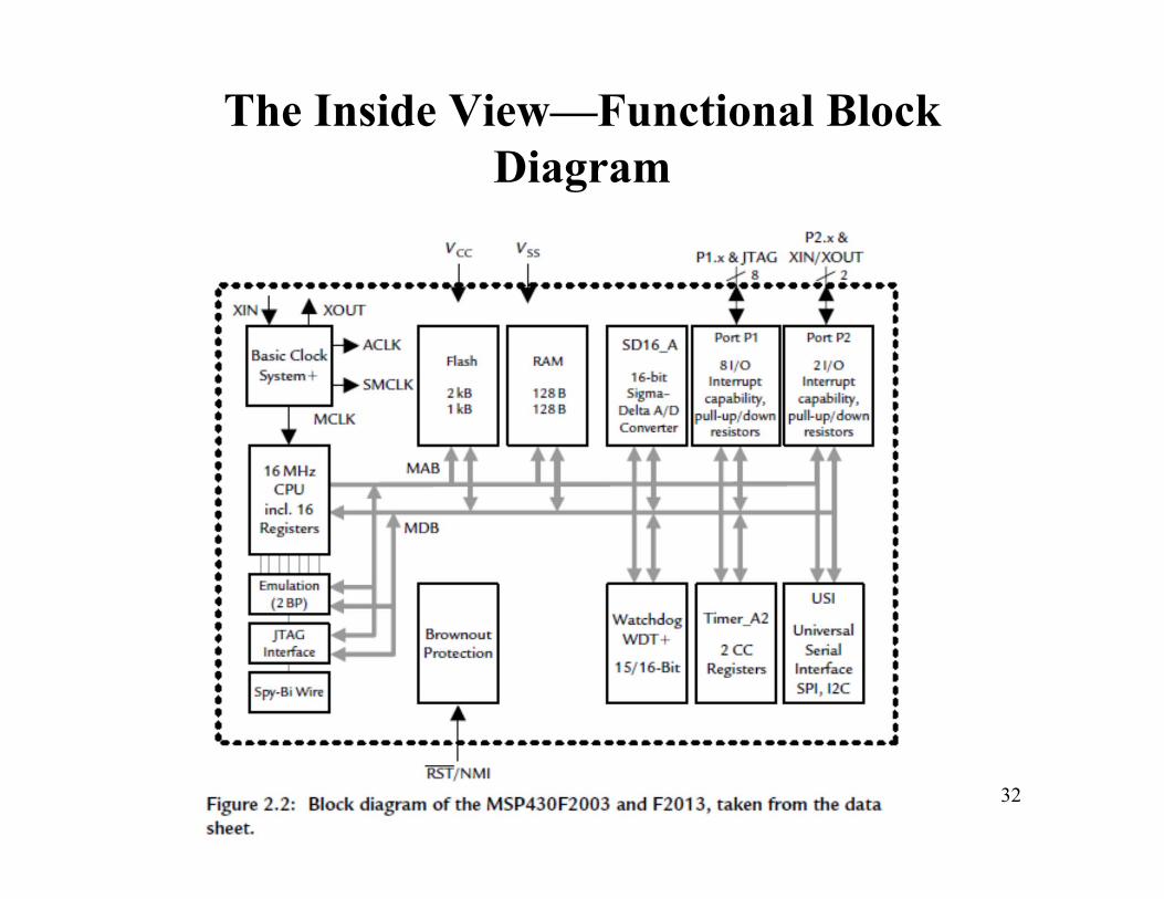
The Inside View—Functional Block Diagram
33

34
Memory
• Each register or pigeonhole holds 8 bits or 1 byte and this is the smallest entity that can be transferred to and from memory
• memory address bus is 16 bits: 0x0000 to 0xFFFF
• The memory data bus is 16 bits wide and can transfer either a word of 16 bits or a byte of 8 bits.

35
Memory address
36
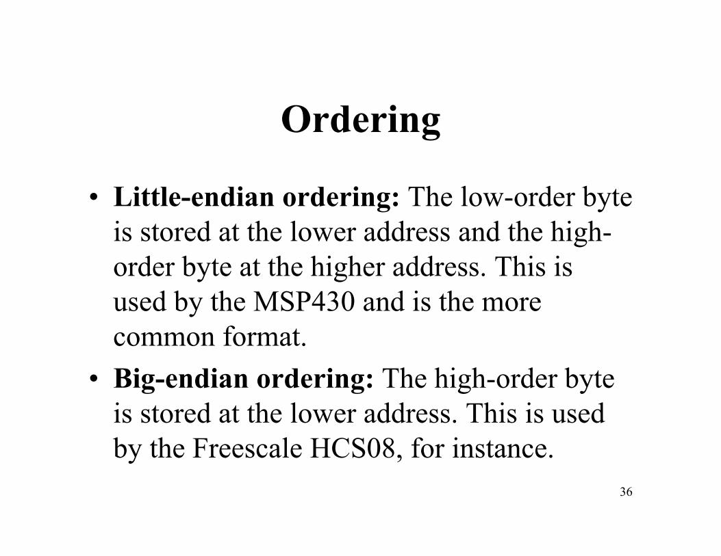
Ordering
• Little-endian ordering: The low-order byte is stored at the lower address and the high-order byte at the higher address. This is used by the MSP430 and is the more common format.
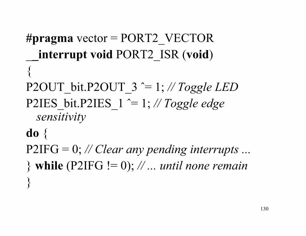
• Big-endian ordering: The high-order byte is stored at the lower address. This is used by the Freescale HCS08, for instance.
37
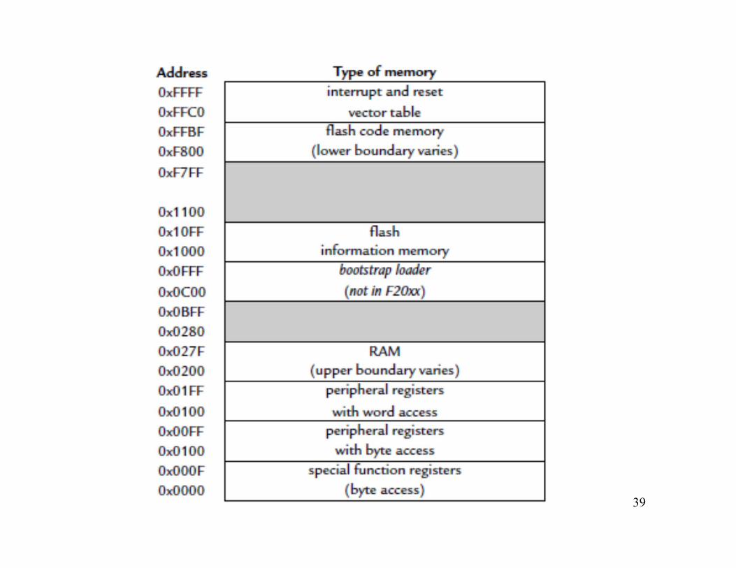
Memory Map• Special function registers: Mostly concerned with enabling
functions of some modules and enabling and signalling interrupts from peripherals.
• Peripheral registers with byte access and peripheral registers with word access: Provide the main communication between the CPU and peripherals. Some must be accessed as words and others as bytes.
• Random access memory: Used for variables. This always starts at address 0x0200 and the upper limit depends on the size of the RAM. The F2013 has 128 B.
• Bootstrap loader: Contains a program to communicate using a standard serial protocol, often with the COM port of a PC.

38
• Information memory: A 256B block of flash memory that is intended for storage of nonvolatile data. This might include serial numbers to identify equipment—an address for a network, for instance—or variables that should be retained even when power is removed. DCO in the MSP430F2xx family and is protected by default.
• Code memory: Holds the program, including the executable code itself and any constant data. The F2013 has 2KB but the F2003 only 1KB.
• Interrupt and reset vectors: Used to handle “exceptions,” when normal operation of the processor is interrupted or when the device is reset. This table was smaller and started at 0xFFE0 in earlier devices.
39
40
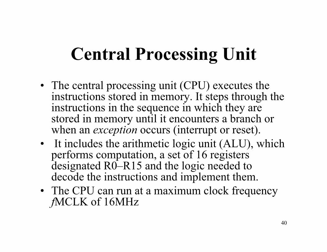
Central Processing Unit• The central processing unit (CPU) executes the
instructions stored in memory. It steps through the instructions in the sequence in which they are stored in memory until it encounters a branch or when an exception occurs (interrupt or reset).
• It includes the arithmetic logic unit (ALU), which performs computation, a set of 16 registers designated R0–R15 and the logic needed to decode the instructions and implement them.
• The CPU can run at a maximum clock frequency fMCLK of 16MHz
41
42
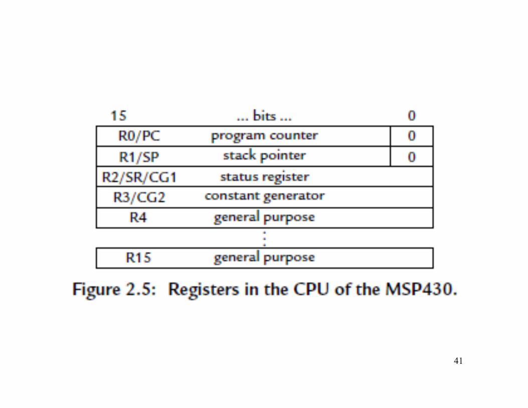
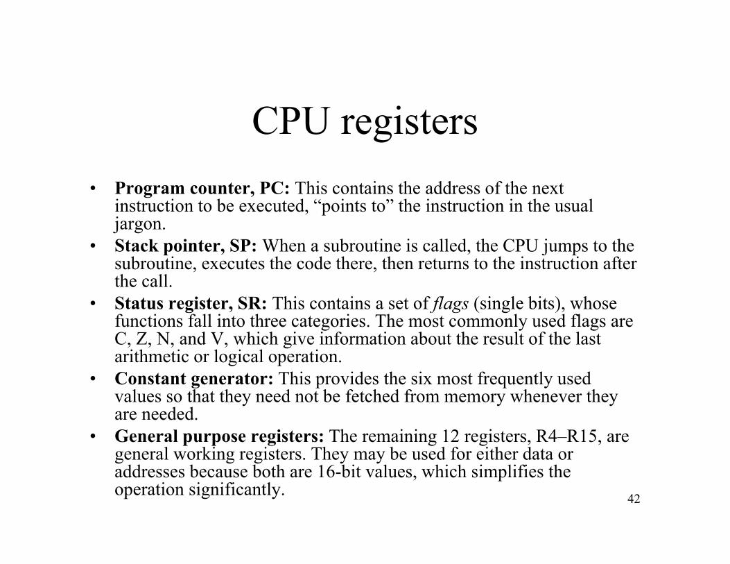
CPU registers• Program counter, PC: This contains the address of the next
instruction to be executed, “points to” the instruction in the usual jargon.
• Stack pointer, SP: When a subroutine is called, the CPU jumps to the subroutine, executes the code there, then returns to the instruction after the call.
• Status register, SR: This contains a set of flags (single bits), whose functions fall into three categories. The most commonly used flags are C, Z, N, and V, which give information about the result of the last arithmetic or logical operation.
• Constant generator: This provides the six most frequently used values so that they need not be fetched from memory whenever they are needed.
• General purpose registers: The remaining 12 registers, R4–R15, are general working registers. They may be used for either data or addresses because both are 16-bit values, which simplifies the operation significantly.
43
Memory-Mapped Input and Output
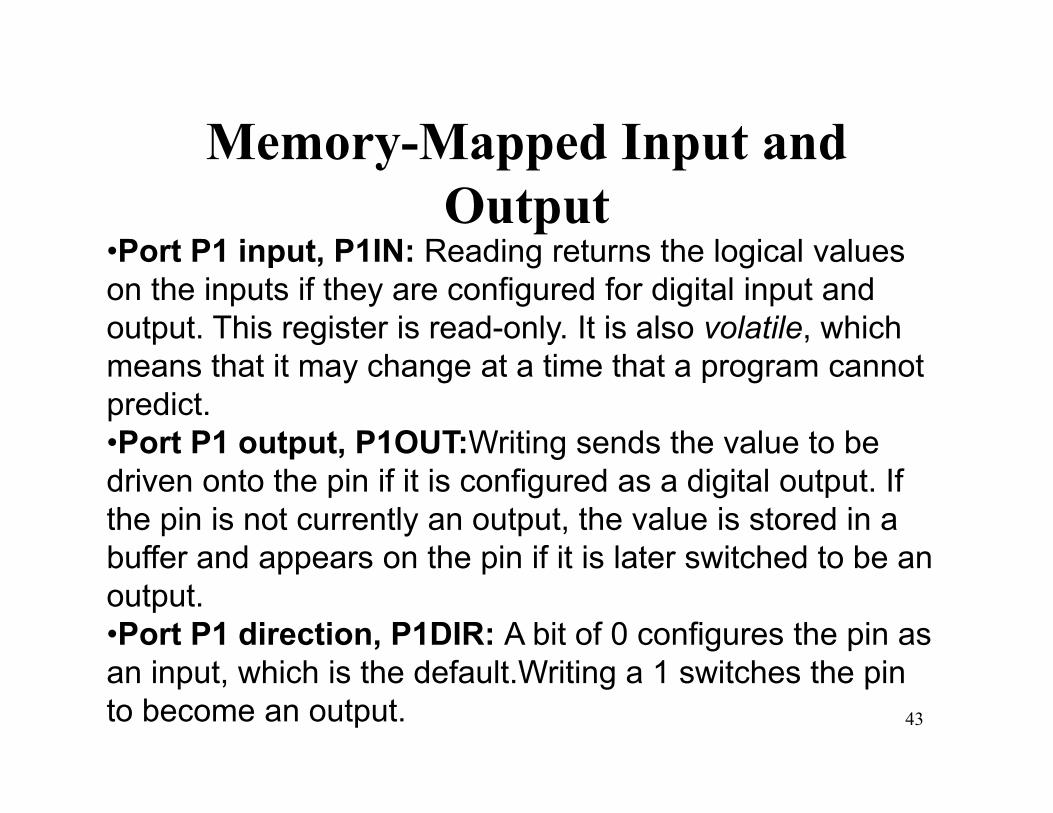
•Port P1 input, P1IN: Reading returns the logical values on the inputs if they are configured for digital input and output. This register is read-only. It is also volatile, which means that it may change at a time that a program cannot predict. •Port P1 output, P1OUT:Writing sends the value to be driven onto the pin if it is configured as a digital output. If the pin is not currently an output, the value is stored in a buffer and appears on the pin if it is later switched to be an output.•Port P1 direction, P1DIR: A bit of 0 configures the pin as an input, which is the default.Writing a 1 switches the pin to become an output.

44
45
Clock Generator• Clock is essential for every synchronous digital system• Usually a crystal with a frequency of a few MHz would be
connected to two pins. It would drive the CPU directly and was typically divided down by a factor of 2 or 4 for the main bus.
• Unfortunately, the conflicting demands for high performance and low power mean that most modern microcontrollers have much more complicated clocks, often with two or more sources.
• In many applications the MCU spends most of its time in a low-power mode until some event occurs, when it must wake up and handle the event rapidly.
46
• Master clock, MCLK, is used by the CPU and a few peripherals.
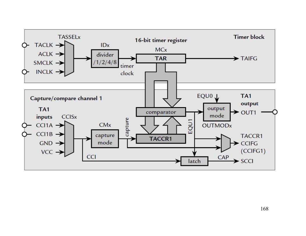
• Subsystem master clock, SMCLK, is distributed to peripherals.
• Auxiliary clock, ACLK, is also distributed to peripherals.
47
• ACLK comes from a low-frequency crystal oscillator, typically at 32 KHz.
• MCLK and SMCLK are supplied from the DCO, which is controlled by a frequency-locked loop (FLL). This locks the frequency at 32 times the ACLK frequency, which is close to 1MHz for the usual watch crystal.
48
Exceptions: Interrupts and Resets
• Interrupts: Usually generated by hardware (although they can be initiated by software) and often indicate that an event has occurred that needs an urgent response. A packet of data might have been received, for instance, and needs to be processed before the next packet arrives. The processor stops what it was doing, stores enough information (the contents of the program counter and status register) for it to resume later on and executes an interrupt service routine (ISR). It returns to its previous activity when the ISR has been completed. Thus an ISR is something like a subroutine called by hardware (at an unpredictable time) rather than software.
• Resets: Again usually generated by hardware, either when power is applied or when something catastrophic has happened and normal operation cannot continue. This can happen accidentally if the watchdog timer has not been disabled, which is easy to forget. A reset causes the device to (re)start from a well-defined state.
49
Where to Find Further Information
• Data Sheet• Family User’s Guide• FET User’s Guide• Application Notes• Code Examples

50
Quizzes
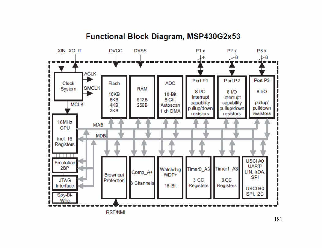
• List CPU registers and their functions • How many clocks signals in TI MSP430G2553?• What are Interrupt Service Routines?
51
Next
• Development• A Simple Tour of the MSP430
52
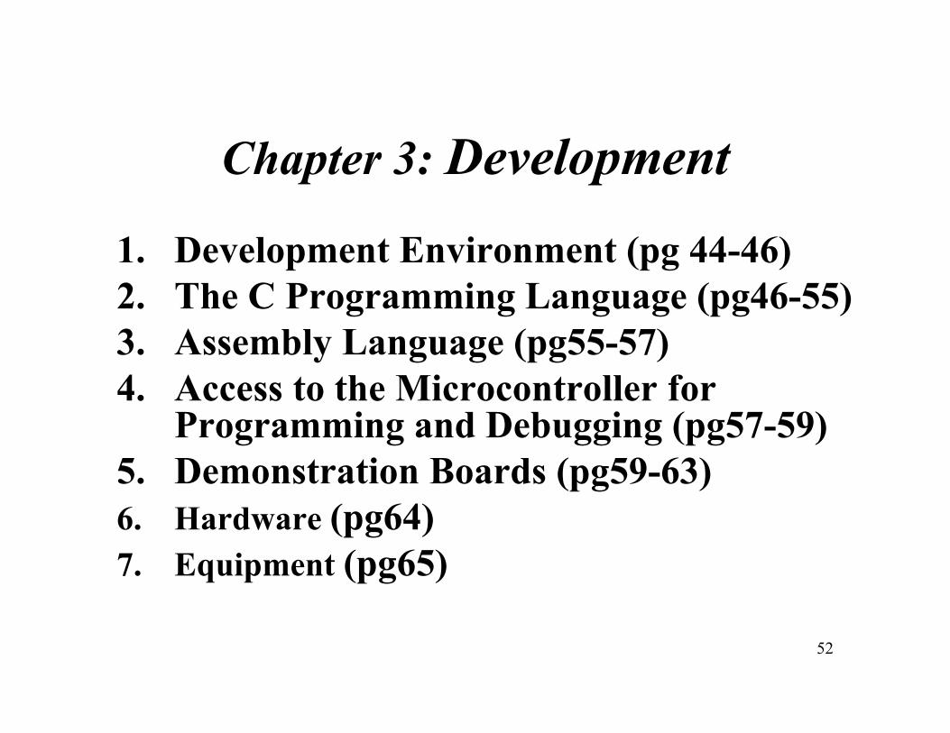
Chapter 3: Development
1. Development Environment (pg 44-46)2. The C Programming Language (pg46-55)3. Assembly Language (pg55-57)4. Access to the Microcontroller for
Programming and Debugging (pg57-59)5. Demonstration Boards (pg59-63)6. Hardware (pg64)7. Equipment (pg65)
53
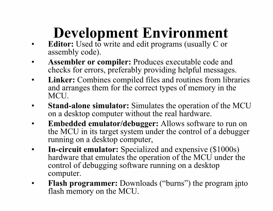
Development Environment• Editor: Used to write and edit programs (usually C or
assembly code). • Assembler or compiler: Produces executable code and
checks for errors, preferably providing helpful messages. • Linker: Combines compiled files and routines from libraries
and arranges them for the correct types of memory in the MCU.
• Stand-alone simulator: Simulates the operation of the MCU on a desktop computer without the real hardware.
• Embedded emulator/debugger: Allows software to run on the MCU in its target system under the control of a debugger running on a desktop computer,
• In-circuit emulator: Specialized and expensive ($1000s) hardware that emulates the operation of the MCU under the control of debugging software running on a desktop computer.
• Flash programmer: Downloads (“burns”) the program into flash memory on the MCU.
54
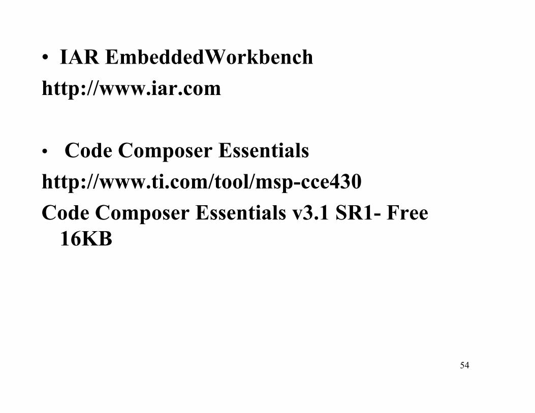
• IAR EmbeddedWorkbenchhttp://www.iar.com
• Code Composer Essentialshttp://www.ti.com/tool/msp-cce430Code Composer Essentials v3.1 SR1- Free
16KB
55
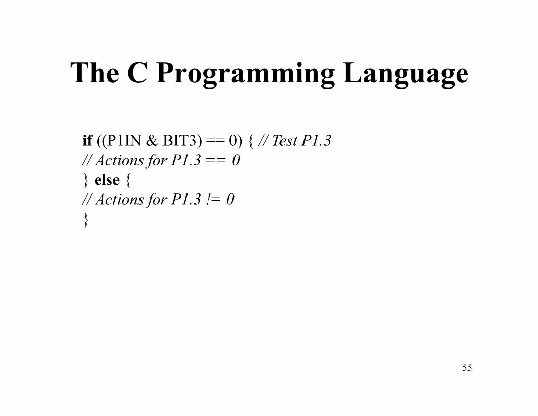
The C Programming Language
if ((P1IN & BIT3) == 0) { // Test P1.3// Actions for P1.3 == 0} else {// Actions for P1.3 != 0}

56
Assembly Languagemov.w #WDTPW|WDTHOLD ,& WDTCTL
57
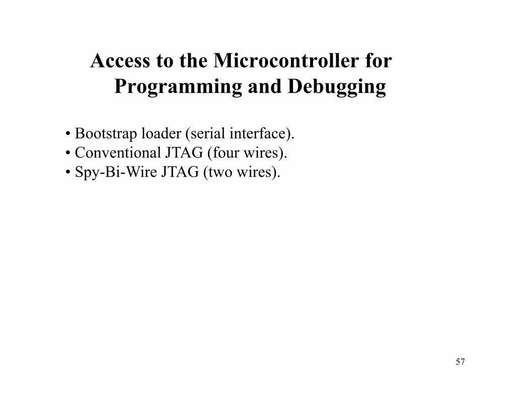
Access to the Microcontroller for Programming and Debugging
• Bootstrap loader (serial interface).• Conventional JTAG (four wires).• Spy-Bi-Wire JTAG (two wires).
58
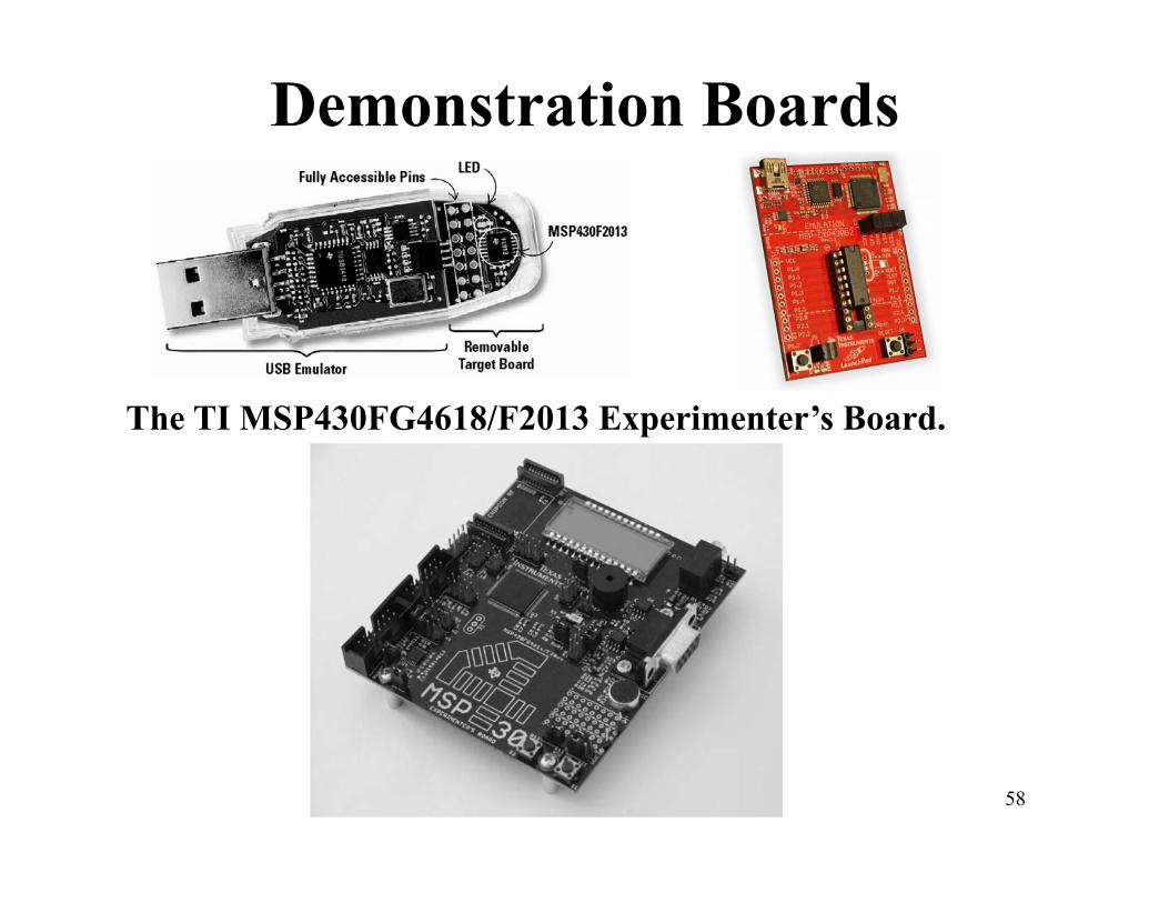
Demonstration Boards
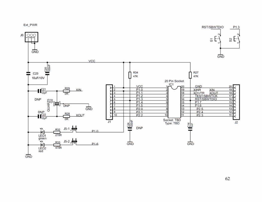
The TI MSP430FG4618/F2013 Experimenter’s Board.

59
Hardware hint• ?
60
A Simple Tour of the MSP430• First Program• Light LEDs in C• Light LEDs in Assembly Language• Read Input from a Switch• Automatic Control: Flashing Light by Software
Delay• Automatic Control: Use of Subroutines• Automatic Control: Flashing a Light by Polling
Timer_A• Header Files and Issues Brushed under the
Carpet

61
62

63

64
First Program
1. #include <stdio.h>2. void main (void)3. {4. printf("hello , world\n");5. }
65
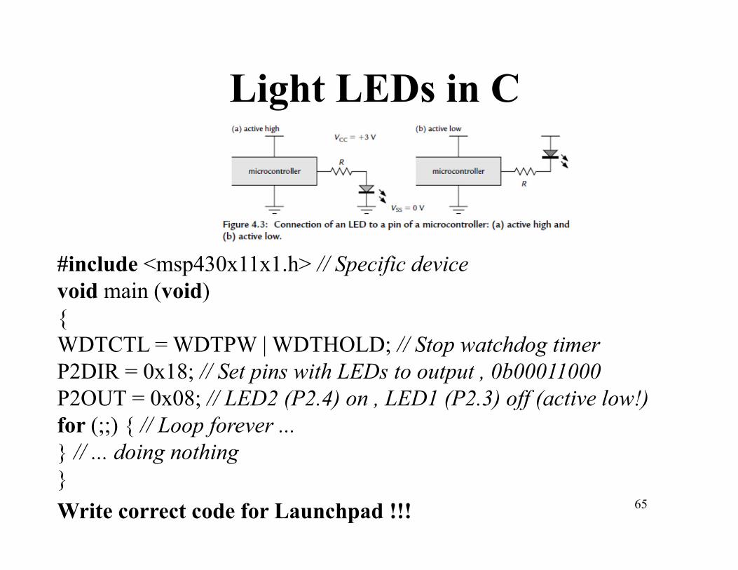
Light LEDs in C
#include <msp430x11x1.h> // Specific devicevoid main (void){WDTCTL = WDTPW | WDTHOLD; // Stop watchdog timerP2DIR = 0x18; // Set pins with LEDs to output , 0b00011000P2OUT = 0x08; // LED2 (P2.4) on , LED1 (P2.3) off (active low!)for (;;) { // Loop forever ...} // ... doing nothing}Write correct code for Launchpad !!!
66
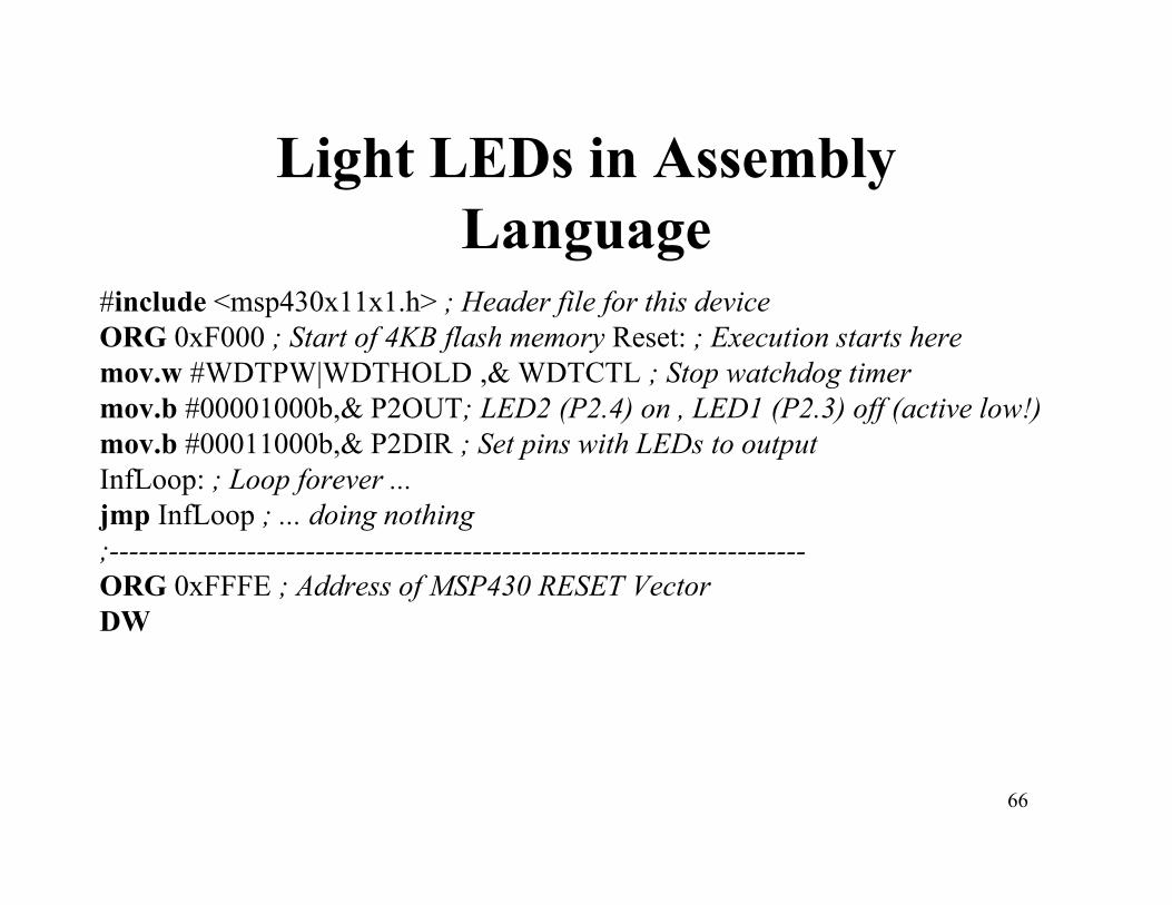
Light LEDs in Assembly Language
#include <msp430x11x1.h> ; Header file for this deviceORG 0xF000 ; Start of 4KB flash memory Reset: ; Execution starts heremov.w #WDTPW|WDTHOLD ,& WDTCTL ; Stop watchdog timermov.b #00001000b,& P2OUT; LED2 (P2.4) on , LED1 (P2.3) off (active low!)mov.b #00011000b,& P2DIR ; Set pins with LEDs to outputInfLoop: ; Loop forever ...jmp InfLoop ; ... doing nothing;-----------------------------------------------------------------------ORG 0xFFFE ; Address of MSP430 RESET VectorDW

67
Read Input from a Switch

68
#include <msp430x11x1.h> // Specific device// Pins for LED and button on port 2#define LED1 BIT3#define B1 BIT1void main (void){WDTCTL = WDTPW | WDTHOLD; // Stop watchdog timerP2OUT |= LED1; // Preload LED1 off (active low!)P2DIR = LED1; // Set pin with LED1 to outputfor (;;) { // Loop foreverif ((P2IN & B1) == 0)
{ // Is button down? (active low)P2OUT &= ˜LED1; // Yes: Turn LED1 on (active low!)}
else {P2OUT |= LED1; // No: Turn LED1 off (active low!)}}
}Write correct code for Launchpad !!!
69
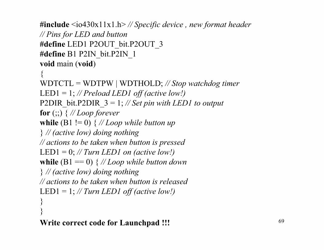
#include <io430x11x1.h> // Specific device , new format header// Pins for LED and button#define LED1 P2OUT_bit.P2OUT_3#define B1 P2IN_bit.P2IN_1void main (void){WDTCTL = WDTPW | WDTHOLD; // Stop watchdog timerLED1 = 1; // Preload LED1 off (active low!)P2DIR_bit.P2DIR_3 = 1; // Set pin with LED1 to outputfor (;;) { // Loop foreverwhile (B1 != 0) { // Loop while button up} // (active low) doing nothing// actions to be taken when button is pressedLED1 = 0; // Turn LED1 on (active low!)while (B1 == 0) { // Loop while button down} // (active low) doing nothing// actions to be taken when button is releasedLED1 = 1; // Turn LED1 off (active low!)}}Write correct code for Launchpad !!!
70
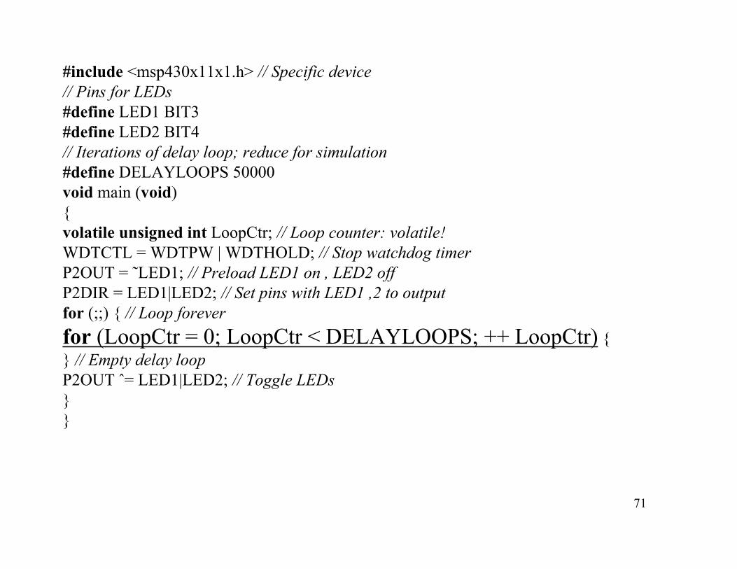
Automatic Control: Flashing Light by Software Delay
• the simplest task is to flash an LED on and off. Let us do this with a period of about 1 Hz, which needs a delay of 0.5 s while the LED remains on or off
71
#include <msp430x11x1.h> // Specific device// Pins for LEDs#define LED1 BIT3#define LED2 BIT4// Iterations of delay loop; reduce for simulation#define DELAYLOOPS 50000void main (void){volatile unsigned int LoopCtr; // Loop counter: volatile!WDTCTL = WDTPW | WDTHOLD; // Stop watchdog timerP2OUT = ˜LED1; // Preload LED1 on , LED2 offP2DIR = LED1|LED2; // Set pins with LED1 ,2 to outputfor (;;) { // Loop foreverfor (LoopCtr = 0; LoopCtr < DELAYLOOPS; ++ LoopCtr) {} // Empty delay loopP2OUT ˆ= LED1|LED2; // Toggle LEDs}}
72
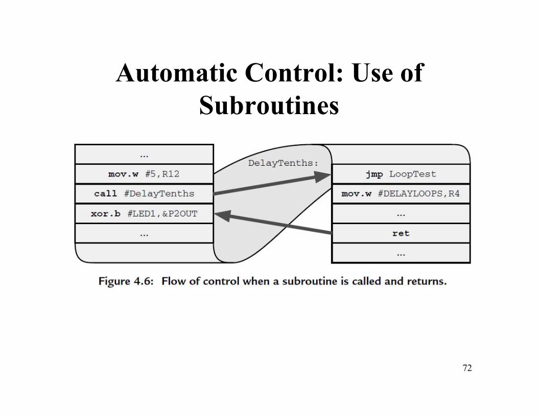
Automatic Control: Use of Subroutines
73
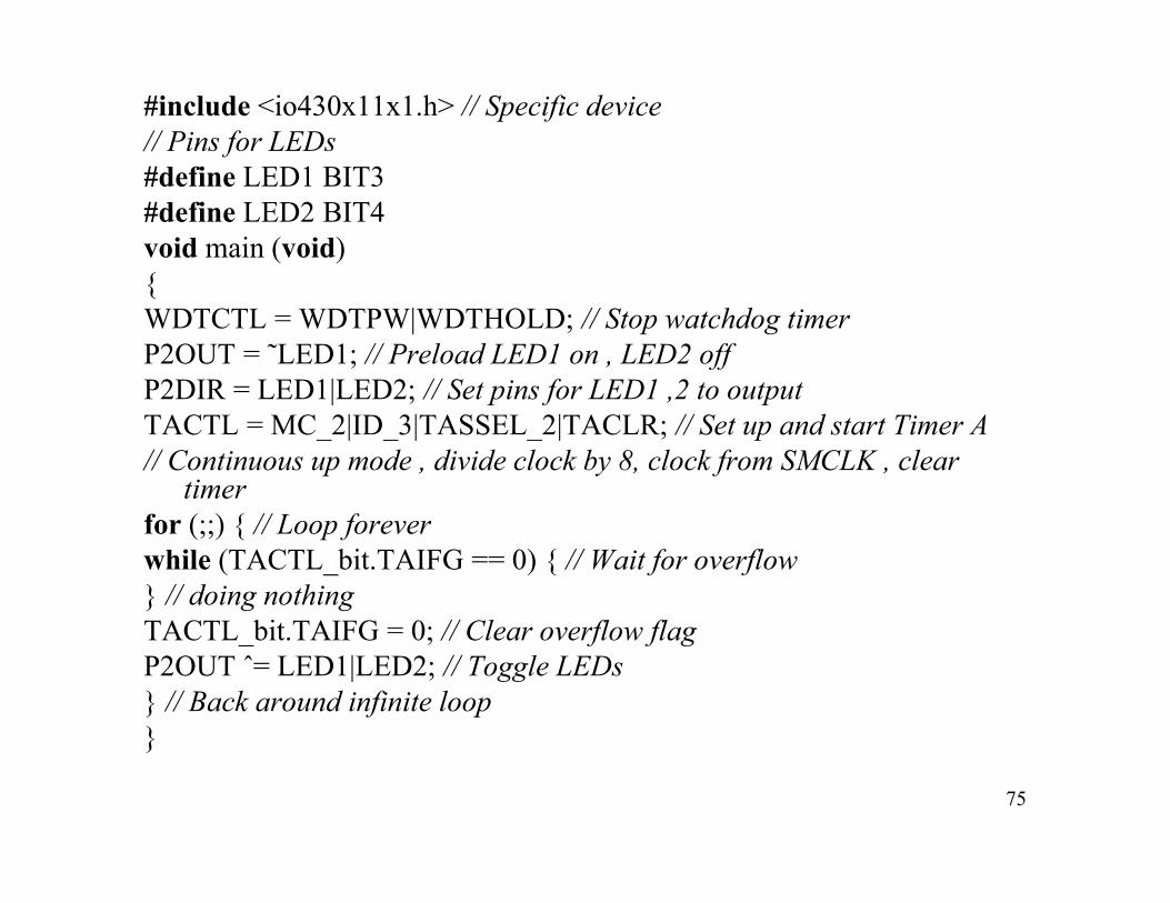
Automatic Control: Flashing a Light by Polling Timer_A
• Software delay loops are a waste of the processor because it is not available for more useful actions.
• Unpredictability of delays written in C. • All microcontrollers therefore have special
hardware to act as a timer.

74
75
#include <io430x11x1.h> // Specific device// Pins for LEDs#define LED1 BIT3#define LED2 BIT4void main (void){WDTCTL = WDTPW|WDTHOLD; // Stop watchdog timerP2OUT = ˜LED1; // Preload LED1 on , LED2 offP2DIR = LED1|LED2; // Set pins for LED1 ,2 to outputTACTL = MC_2|ID_3|TASSEL_2|TACLR; // Set up and start Timer A// Continuous up mode , divide clock by 8, clock from SMCLK , clear
timerfor (;;) { // Loop foreverwhile (TACTL_bit.TAIFG == 0) { // Wait for overflow} // doing nothingTACTL_bit.TAIFG = 0; // Clear overflow flagP2OUT ˆ= LED1|LED2; // Toggle LEDs} // Back around infinite loop}
76
Timer_A in Up Mode
• The maximum desired value of the count is programmed into another register, TACCR0. In this mode TAR starts from 0 and counts up to the value in TACCR0, after which it returns to 0 and sets TAIFG. Thus the period is TACCR0+1 counts.
• The clock has been divided down to 100 KHz so we need 50,000 counts for a delay of 0.5 s and should therefore store 49,999 in TACCR0.

77
Quizzes• List all techniques to flash a led?
78
What is next?
• CHAPTER 5: Architecture of the MSP430 Processor (Page 119-175)
79
Chapter 5: Architecture of the MSP430 Processor
1. Central Processing Unit (pg 120-125)2. Addressing Modes (pg125-131)3. Constant Generator and Emulated Instructions
(pg131-132)4. Instruction Set(pg132-146)5. Examples(pg146-153)6. Reflections on the CPU and Instruction Set
(pg153-157)7. Resets (pg157-163)8. Clock System (pg163- 175)

80

81
Central Processing Unit
• Program Counter (PC)• Stack Pointer (SP)• Status Register (SR)• Constant Generators• General-Purpose Registers
82
Addressing Modes
• Just only for Assembly Programmers
83
Constant Generator and Emulated Instructions
• Just only for Assembly Programmers
84
Instruction Set
• Movement Instructionsmov.w src ,dst ;// dst=src; //c -prg
• Arithmetic and Logic Instructions with Two Operandsadd.w src ,dst // dst += src; //c -prg
• Shift and Rotate Instructionsand.w src ,dst ; // dst &= src
• Flow of Control• …
85
Examples
add.w src ,dst ; add dst += srcaddc.w src ,dst ; add with carry dst += (src + C)adc.w dst ; add carry bit dst += C emulatedsub.w src ,dst ; subtract dst -= srcsubc.w src ,dst ; subtract with borrow dst -= (src +
˜C)
86
Reflections on the CPU and Instruction Set
• Simplicity• Registers of the CPU• Is the MSP430 a RISC—and Should It
Be?• Addressing Modes
87
Resets
• A reset is a sequence of operations that puts the device into a well-defined state, from which the user’s program may start– Power-on Reset (POR)
• The device is powered up. More generally, a POR is raised if the supply voltage drops to so low a value that the device may not work correctly: a brownout.
– Power-up Clear (PUC)• The watchdog timer overflows in watchdog mode.
88
Clock System
• Master clock, MCLK is used by the CPU and a few peripherals.
• Sub-system master clock, SMCLK is distributed to peripherals.
• Auxiliary clock, ACLK is also distributed to peripherals.

89

90
91
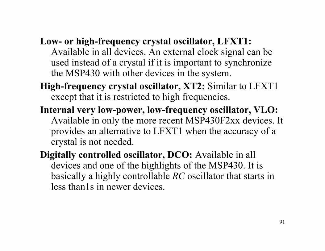
Low- or high-frequency crystal oscillator, LFXT1: Available in all devices. An external clock signal can be used instead of a crystal if it is important to synchronize the MSP430 with other devices in the system.
High-frequency crystal oscillator, XT2: Similar to LFXT1 except that it is restricted to high frequencies.
Internal very low-power, low-frequency oscillator, VLO: Available in only the more recent MSP430F2xx devices. It provides an alternative to LFXT1 when the accuracy of a crystal is not needed.
Digitally controlled oscillator, DCO: Available in all devices and one of the highlights of the MSP430. It is basically a highly controllable RC oscillator that starts in less than1s in newer devices.
92
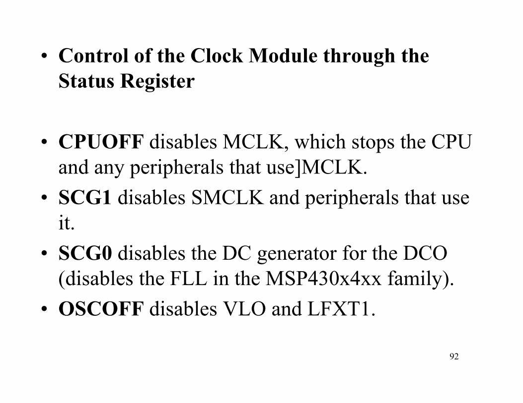
• Control of the Clock Module through the Status Register
• CPUOFF disables MCLK, which stops the CPU and any peripherals that use]MCLK.
• SCG1 disables SMCLK and peripherals that use it.
• SCG0 disables the DC generator for the DCO (disables the FLL in the MSP430x4xx family).
• OSCOFF disables VLO and LFXT1.
93
Quizzes
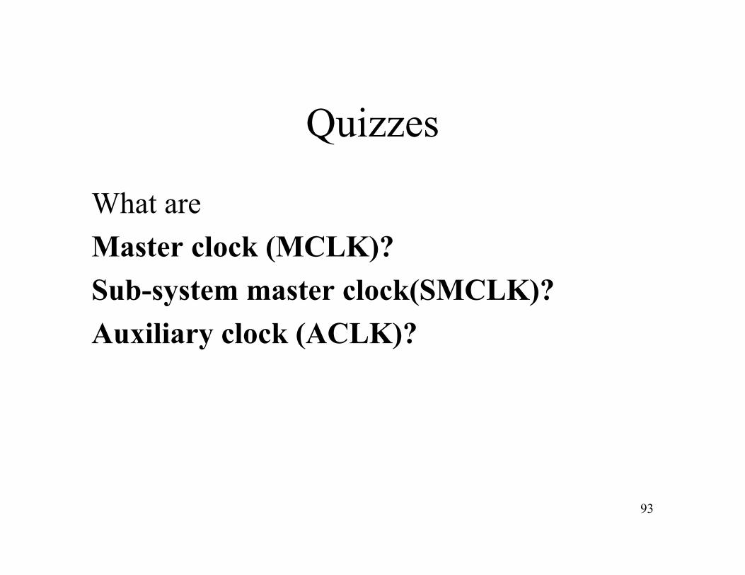
What areMaster clock (MCLK)?Sub-system master clock(SMCLK)?Auxiliary clock (ACLK)?
94
What is next?
• CHAPTER 6: Functions, Interrupts, and Low-Power Modes (Page 177-205)
95
Hệ thống nhúng
Ts. Lê Mạnh HảiKhoa CNTT,
ĐH Kỹ thuật Công nghệ TP HCM
Embedded Systems
96
Chapter 6: Functions, Interrupts, and Low-Power Modes
1. Functions and Subroutines2. What Happens when a Subroutine Is Called?3. Storage for Local Variables4. Passing Parameters5. Example Mixing C and Assembly Language6. Interrupts7. What Happens when an Interrupt Is Requested?8. Interrupt Service Routines9. Issues Associated with Interrupts10. Low-Power Modes of Operation
97
Functions and Subroutines• A well-structured program should be divided into
separate modules—functions in C or subroutines in assembly language
• It is particularly important to understand the central role of the stack
• Interrupts are a major feature of most embedded software. They are vaguely like functions that are called by hardware rather than software.
• The final topic in this chapter is the range of low-power modes of operation. They are described here because the MSP430 needs an interrupt to wake it from a low-power mode.
98
Functions and Subroutines
• It makes programs easier to write and more reliable to test and maintain
• Functions can readily be reused and incorporated into libraries, provided that their documentation is clear

99
What Happens when a Subroutine Is Called?
• The address of the subroutine is then loaded into the PC and execution continues from there.
• At the end of the subroutine the ret instruction pops the return address off the stack into the PC so that execution resumes with the instruction following the call of the subroutine.
• The return operation is so straightforward that ret is emulated with a mov instruction
100
Storage for Local Variables• CPU registers are simple and fast.• A second approach is to use a fixed location in RAM, • The third approach is to allocate variables on the stack and is generally used when a program has run out of CPU registers. This can be slow in older designs of processors, but the MSP430 can address variables on the stack with its generalindexed and indirect modes. Of course it is still faster to use registers in the CPU when these are available.

101
Passing Parameters
• They are like functions but with the critical distinction that they are requested by hardware at unpredictable times rather than called by software in an orderly manner.
102
ExamplMixing C and Assembly Language
103
Interrupts
• Interrupts are commonly used for a range of applications:– Urgent tasks that must be executed promptly at higher
priority than the main code. However, it is even faster to execute a task directly by hardware if this is possible.
– Infrequent tasks, such as handling slow input from humans. This saves the overhead of regular polling.
– Waking the CPU from sleep. – Calls to an operating system.
104
Interrupts Service Routine
• The code to handle an interrupt is called an interrupt handler or interrupt service routine (ISR).
• It looks superficially like a function but there are a few crucial modifications. – The feature that interrupts arise at unpredictable times
means that an ISR must carry out its action and clean up thoroughly so that the main code can be resumed without error—it should not be able to tell that an interrupt occurred.

105
Interrupt Flags
• Each interrupt has a flag, which is raised (set) when the condition for the interrupt occurs. For example, Timer_A sets the TAIFG flag in the TACTL register when the counter TAR returns to 0.
• Most interrupts are maskable, which means that they are effective only if the general interrupt enable (GIE) bit is set in the status register (SR). They are ignored if GIE is clear.
106
Interrupt vector
• The MSP430 uses vectored interrupts, which means that the address of each ISR—its vector—is stored in a vector table at a defined address in memory.
• Each interrupt vector has a distinct priority, which is used to select which vector is taken if more than one interrupt is active when the vector is fetched. The priorities are fixed in hardware and cannot be changed by the user.
107
What Happens when an Interrupt Is Requested?
1. Any currently executing instruction is completed if the CPU was active when the interrupt was requested. MCLK is started if the CPU was off.
2. The PC, which points to the next instruction, is pushed onto the stack.
3. The SR is pushed onto the stack.4. The interrupt with the highest priority is selected if multiple
interrupts are waiting for service.5. The interrupt request flag is cleared automatically for vectors that
have a single source. Flags remain set for servicing by software if the vector has multiple sources, which applies to the example of TAIFG.
6. The SR is cleared, which has two effects. 7. The interrupt vector is loaded into the PC and the CPU starts to
execute the interrupt service routine at that address.
108
latency
• The delay between an interrupt being requested and the start of the ISR is called the latency.
• If the CPU is already running it is given by the time to execute the current instruction, which might only just have started when the interrupt was requested, plus the six cycles needed to execute the launch sequence.
109
Interrupt Service Routines
• Interrupt Service Routines in C

110
void main (void){WDTCTL = WDTPW|WDTHOLD; // Stop watchdog timerP2OUT = ˜LED1; // Preload LED1 on , LED2 offP2DIR = LED1|LED2; // Set pins with LED1 ,2 to outputTACCR0 = 49999; // Upper limit of count for TARTACCTL0 = CCIE; // Enable interrupts on Compare 0TACTL = MC_1|ID_3|TASSEL_2|TACLR; // Set up and start Timer A// "Up to CCR0" mode , divide clock by 8, clock from SMCLK , clear timer__enable _interrupt (); // Enable interrupts (intrinsic)for (;;) { // Loop forever doing nothing} // Interrupts do the work}// ----------------------------------------------------------------------// Interrupt service routine for Timer A channel 0#pragma vector = TIMERA0_VECTOR__interrupt void TA0_ISR (void){P2OUT ˆ= LED1|LED2; // Toggle LEDs}
111
Nonmaskable Interrupts
• There are a few small differences in the handling of nonmaskable interrupts Three modules can request a nonmaskable interrupt:– Oscillator fault, OFIFG. – Access violation to flash memory, ACCVIFG.– An active edge on the external RST/NMI pin if
it has been configured for interrupts rather than reset.

112
Issues Associated with Interrupts
• Keep Interrupt Service Routines Short (why?)
• Configure Interrupts Carefully• Define All Interrupt Vectors• The Shared Data Problem
113
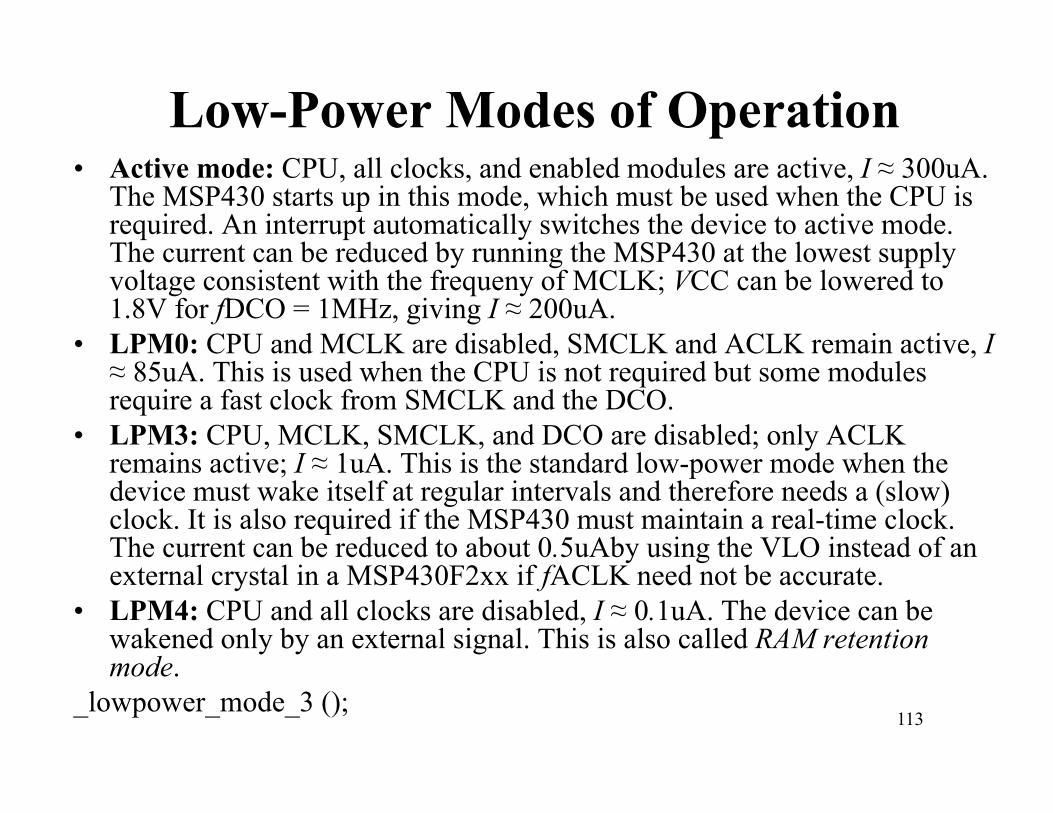
Low-Power Modes of Operation• Active mode: CPU, all clocks, and enabled modules are active, I ≈ 300uA.
The MSP430 starts up in this mode, which must be used when the CPU is required. An interrupt automatically switches the device to active mode. The current can be reduced by running the MSP430 at the lowest supply voltage consistent with the frequeny of MCLK; VCC can be lowered to 1.8V for fDCO = 1MHz, giving I ≈ 200uA.
• LPM0: CPU and MCLK are disabled, SMCLK and ACLK remain active, I ≈ 85uA. This is used when the CPU is not required but some modules require a fast clock from SMCLK and the DCO.
• LPM3: CPU, MCLK, SMCLK, and DCO are disabled; only ACLK remains active; I ≈ 1uA. This is the standard low-power mode when the device must wake itself at regular intervals and therefore needs a (slow) clock. It is also required if the MSP430 must maintain a real-time clock. The current can be reduced to about 0.5uAby using the VLO instead of an external crystal in a MSP430F2xx if fACLK need not be accurate.
• LPM4: CPU and all clocks are disabled, I ≈ 0.1uA. The device can be wakened only by an external signal. This is also called RAM retention mode.
_lowpower_mode_3 ();

114
Quizzes
Why Interrupt is important for embedded system?
What are flags?What is GIE bit?
115
What is next?
• CHAPTER 7: Digital Input, Output, and Displays (Page 207-274)
116
Chapter 7: Digital Input, Output, and Displays
1. Digital Input and Output: Parallel Ports ( 208-216)2. Digital Inputs (216-225)3. Switch Debounce (225-238)4. Digital Outputs (238-243)5. Interface between 3V and 5V Systems (243-247)6. Driving Heavier Loads (247-252)7. Liquid Crystal Displays (252-256)8. Driving an LCD from an MSP430x4xx (256-264)9. Simple Applications of the LCD (264-275)

117
118
Digital Input and Output: Parallel Ports
• The most straightforward form of input and output is through the digital input/output ports using binary values (low or high, corresponding to 0 or 1).
• We already used these for driving LEDs and reading switches. In this section we look at their wider capabilities.

119
Digital Input and Output• There are 10–80 input/output pins on different devices
in the current portfolio of MSP430s; • The F20xx has one complete 8-pin port and 2 pins on a
second port, whilethe largest devices have ten full ports.
• Almost all pins can be used either for digital input/output or for other functions and their operation must be configured when the device starts up.
• This can be tricky. For example, pin P1.0 on the F2013 can be a digital input, digital output, input TACLK, output ACLK, or analog input A0+.
120
121
Digital Input and Output
• Port P1 input, P1IN: reading returns the logical values on the inputs if they are configured for digital input/output.
• Port P1 output, P1OUT: writing sends the value to be driven to each pin if it is configured as a digital output. If the pin is not currently an output, the value is stored in a buffer and appears on the pin if it is later switched to be an output. This register is not initialized and you should therefore write to P1OUT before configuring the pin for output.
122
Digital Input and Output•Port P1 direction, P1DIR: clearing a bit to 0 configures a pin as an input, which is the default in most cases.Writing a 1 switches the pin to become an output. This is for digital input and output; the register works differently if other functions are selected using P1SEL.•Port P1 resistor enable, P1REN: setting a bit to 1 activates a pull-up or pull-down resistor on a pin. Pull-ups are often used to connect a switch to an input as in the section “Read Input from a Switch” on page 80. The resistors are inactive by default (0). When the resistor is enabled (1), the corresponding bit of the P1OUT register selects whether the resistor pulls the input up to VCC (1) or down to VSS (0).•Port P1 selection, P1SEL: selects either digital input/output (0, default) or an alternative function (1). Further registers may be needed to choose the particular function.
123
Digital Input and Output• Port P1 interrupt enable, P1IE: enables interrupts when the
value on an input pin changes. This feature is activated by setting appropriate bits of P1IE to 1. Interrupts are off (0) by default. The whole port shares a single interrupt vector although pins can be enabled individually.
• Port P1 interrupt edge select, P1IES: can generate interrupts either on a positive edge (0), when the input goes from low to high, or on a negative edge from high to low (1). This register is not initialized and should therefore be set up before interrupts are enabled.
• Port P1 interrupt flag, P1IFG: a bit is set when the selected transition has been detected on the input. In addition, an interrupt is requested if it has been enabled. These bits can also be set by software, which provides a mechanism for generating a software interrupt (SWI).
124
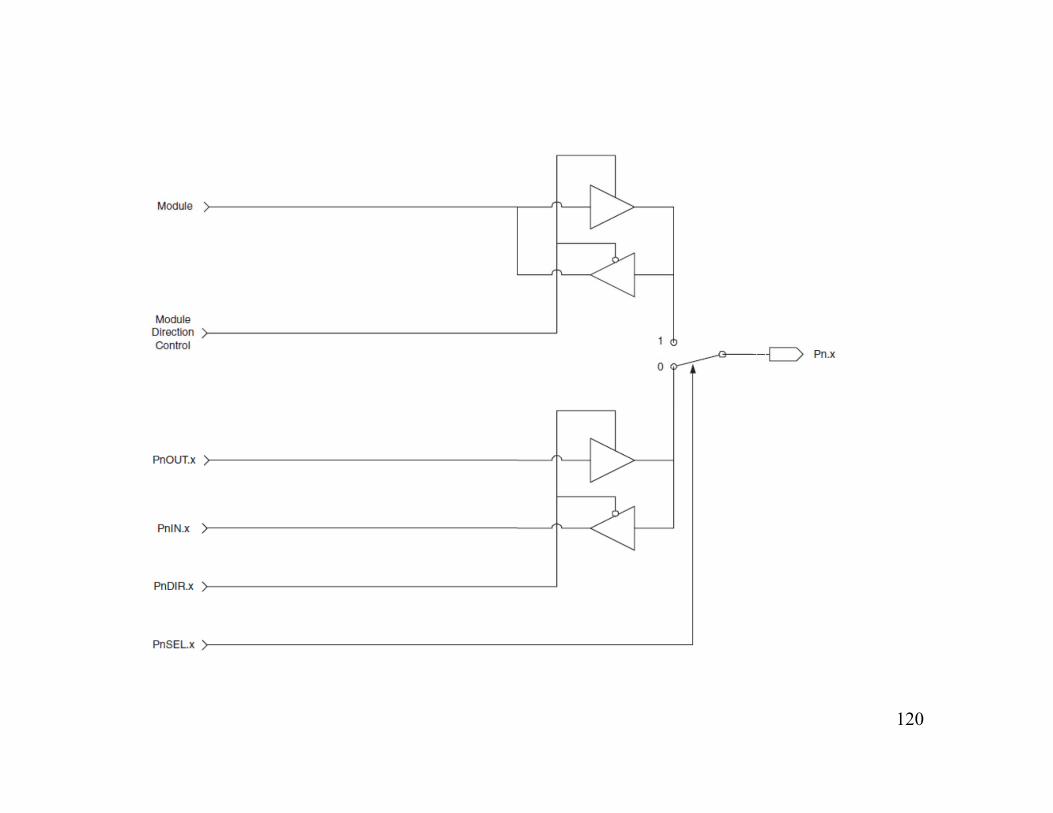
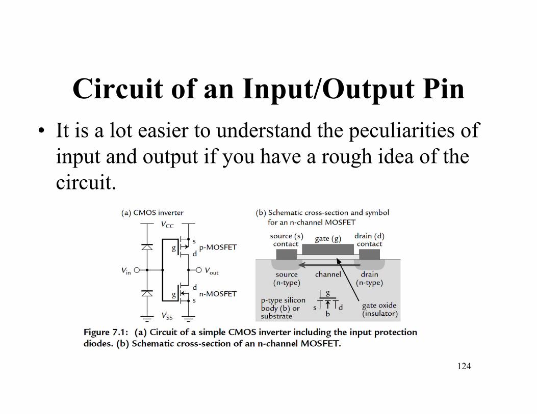
Circuit of an Input/Output Pin• It is a lot easier to understand the peculiarities of
input and output if you have a rough idea of the circuit.
125
Configuration of Unused Pins
• Unused pins must never be left unconnected in their default state as inputs.
• This follows a general rule that inputs to CMOS must never be left unconnected or “floating.” A surprising number of problems can be caused by floating inputs.
• The most trivial is that the input circuit draws an excessive current from the power supply

126
Configuration of Unused PinsThere are three ways of avoiding these problems:1. Wire the unused pins externally to a well-defined voltage,
either VSS or VCC, and configure them as inputs. The danger with this is that you might damage the MCU if the pins are accidentally configured as outputs.
2. Leave the pins unconnected externally but connect them internally to either VSS or VCC by using the pull-down or pull-up resistors. They are again configured as inputs. I prefer this approach but it is restricted to the MSP430F2xx family because the others lack internal pull resistors.
3. Leave the pins unconnected and configure them as outputs.
127
Digital Inputs
• Interrupts on Digital Inputs– Interrupts for port P1 are controlled by the
registers P1IE and P1IES
128
Interrupt vector
• There is a single vector for each port, so the user must check P1IFG to determine the bit that caused the interrupt.
• This bit must be cleared explicitly; it does not happen automatically as with interrupts that have a single source.
129
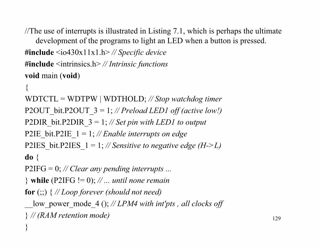
//The use of interrupts is illustrated in Listing 7.1, which is perhaps the ultimate development of the programs to light an LED when a button is pressed.
#include <io430x11x1.h> // Specific device#include <intrinsics.h> // Intrinsic functionsvoid main (void){WDTCTL = WDTPW | WDTHOLD; // Stop watchdog timerP2OUT_bit.P2OUT_3 = 1; // Preload LED1 off (active low!)P2DIR_bit.P2DIR_3 = 1; // Set pin with LED1 to outputP2IE_bit.P2IE_1 = 1; // Enable interrupts on edgeP2IES_bit.P2IES_1 = 1; // Sensitive to negative edge (H->L)do {P2IFG = 0; // Clear any pending interrupts ...} while (P2IFG != 0); // ... until none remainfor (;;) { // Loop forever (should not need)__low_power_mode_4 (); // LPM4 with int'pts , all clocks off} // (RAM retention mode)}
130
#pragma vector = PORT2_VECTOR__interrupt void PORT2_ISR (void){P2OUT_bit.P2OUT_3 ˆ= 1; // Toggle LEDP2IES_bit.P2IES_1 ˆ= 1; // Toggle edge
sensitivitydo {P2IFG = 0; // Clear any pending interrupts ...} while (P2IFG != 0); // ... until none remain}
131
Multiplexed Inputs: Scanning a Matrix Keypad
• Many products require numerical input and provide a keypad for the user.
• These often have 12 keys, like a telephone, or more. An individual connection for each switch would use an exorbitant number of pins so they are usually arranged as a matrix instead.

132
133
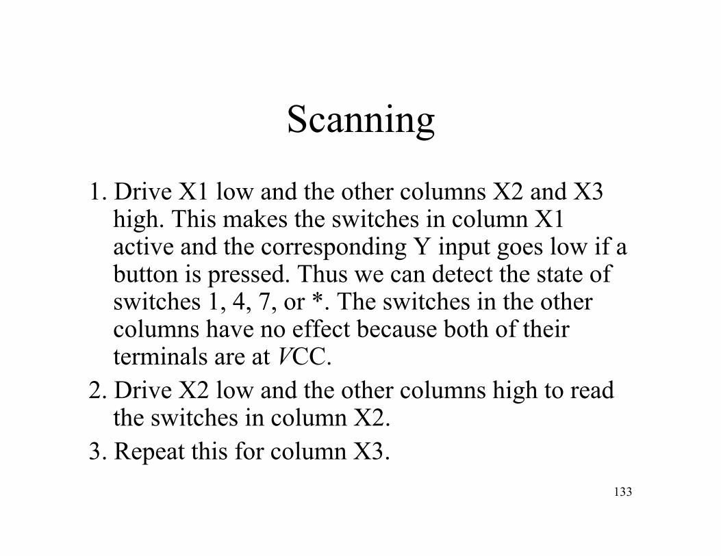
Scanning
1. Drive X1 low and the other columns X2 and X3 high. This makes the switches in column X1 active and the corresponding Y input goes low if a button is pressed. Thus we can detect the state of switches 1, 4, 7, or *. The switches in the other columns have no effect because both of their terminals are at VCC.
2. Drive X2 low and the other columns high to read the switches in column X2.
3. Repeat this for column X3.
134
Switch Debounce
• Older textbooks tell you that bounce is worse when a switch is closed than when it is opened and may last for around 50 ms.
135
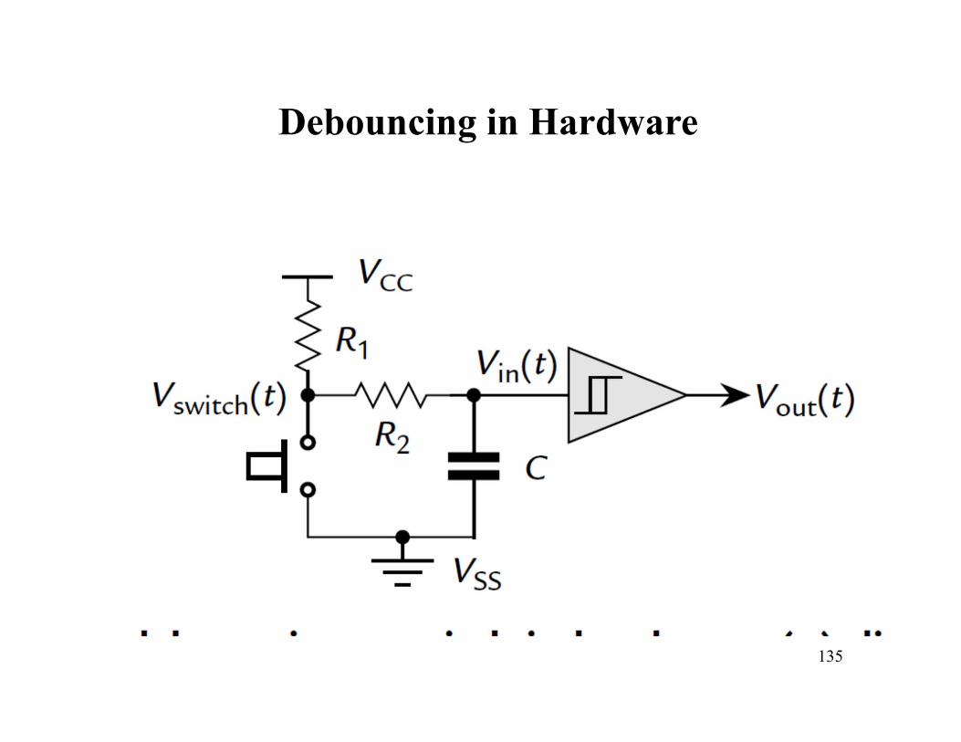
Debouncing in Hardware

136
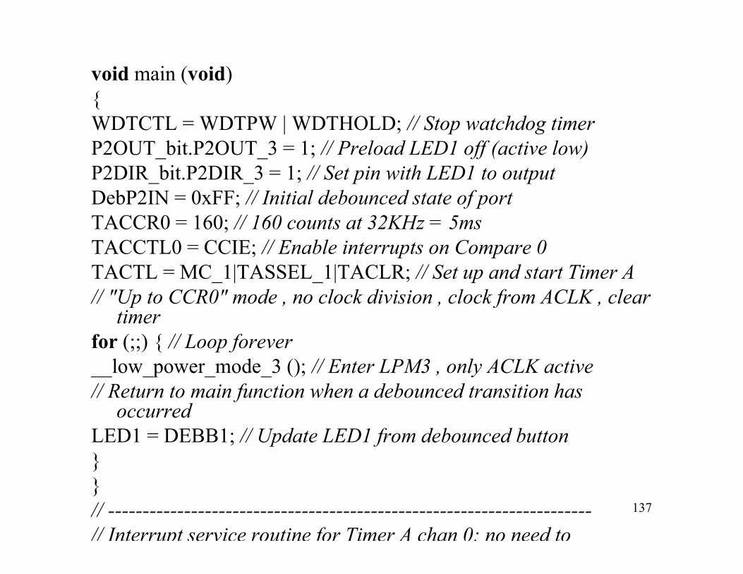
Debouncing in Software#include <io430x11x1.h> // Specific device#include <intrinsics.h> // Intrinsic functions#include <stdint.h> // Standard integer typesunion { // Debounced state of P2INunsigned char DebP2IN; // Complete bytestruct {unsigned char DebP2IN_0 : 1;unsigned char DebP2IN_1 : 1;unsigned char DebP2IN_2 : 1;unsigned char DebP2IN_3 : 1;unsigned char DebP2IN_4 : 1;unsigned char DebP2IN_5 : 1;unsigned char DebP2IN_6 : 1;unsigned char DebP2IN_7 : 1;} DebP2IN_bit; // Individual bits};#define RAWB1 P2IN_bit.P2IN_1#define DEBB1 DebP2IN_bit.DebP2IN_1#define LED1 P2OUT_bit.P2OUT_3
137
void main (void){WDTCTL = WDTPW | WDTHOLD; // Stop watchdog timerP2OUT_bit.P2OUT_3 = 1; // Preload LED1 off (active low)P2DIR_bit.P2DIR_3 = 1; // Set pin with LED1 to outputDebP2IN = 0xFF; // Initial debounced state of portTACCR0 = 160; // 160 counts at 32KHz = 5msTACCTL0 = CCIE; // Enable interrupts on Compare 0TACTL = MC_1|TASSEL_1|TACLR; // Set up and start Timer A// "Up to CCR0" mode , no clock division , clock from ACLK , clear
timerfor (;;) { // Loop forever__low_power_mode_3 (); // Enter LPM3 , only ACLK active// Return to main function when a debounced transition has
occurredLED1 = DEBB1; // Update LED1 from debounced button}}// ----------------------------------------------------------------------// Interrupt service routine for Timer A chan 0; no need to
138
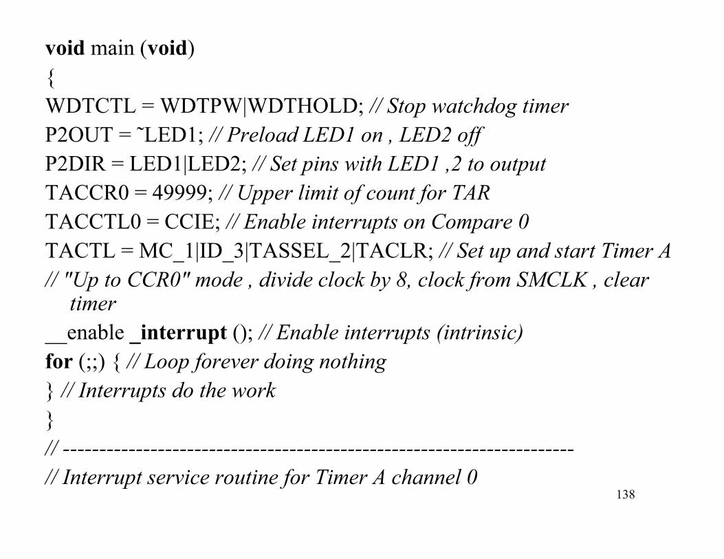
void main (void){WDTCTL = WDTPW|WDTHOLD; // Stop watchdog timerP2OUT = ˜LED1; // Preload LED1 on , LED2 offP2DIR = LED1|LED2; // Set pins with LED1 ,2 to outputTACCR0 = 49999; // Upper limit of count for TARTACCTL0 = CCIE; // Enable interrupts on Compare 0TACTL = MC_1|ID_3|TASSEL_2|TACLR; // Set up and start Timer A// "Up to CCR0" mode , divide clock by 8, clock from SMCLK , clear
timer__enable _interrupt (); // Enable interrupts (intrinsic)for (;;) { // Loop forever doing nothing} // Interrupts do the work}// ----------------------------------------------------------------------// Interrupt service routine for Timer A channel 0
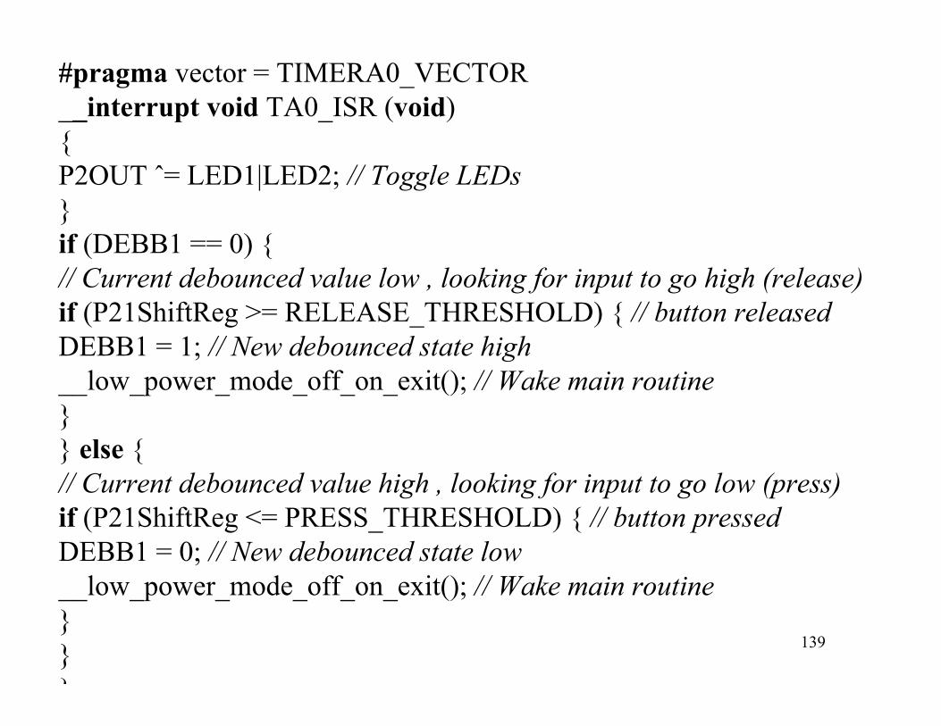
139
#pragma vector = TIMERA0_VECTOR__interrupt void TA0_ISR (void){P2OUT ˆ= LED1|LED2; // Toggle LEDs}if (DEBB1 == 0) {// Current debounced value low , looking for input to go high (release)if (P21ShiftReg >= RELEASE_THRESHOLD) { // button releasedDEBB1 = 1; // New debounced state high__low_power_mode_off_on_exit(); // Wake main routine}} else {// Current debounced value high , looking for input to go low (press)if (P21ShiftReg <= PRESS_THRESHOLD) { // button pressedDEBB1 = 0; // New debounced state low__low_power_mode_off_on_exit(); // Wake main routine}}}
140
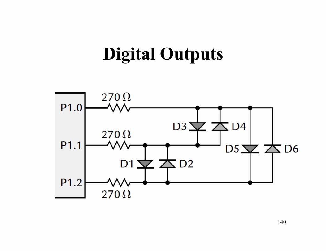
Digital Outputs
141

142
• http://www.youtube.com/watch?v=pOlhQ0n552Y&lr=1
143
Quizzes
Name some Registers for Port1?What are P1REN?How to scanning matrix keyboard?

144
What is next?
• CHAPTER 7: LCD
145
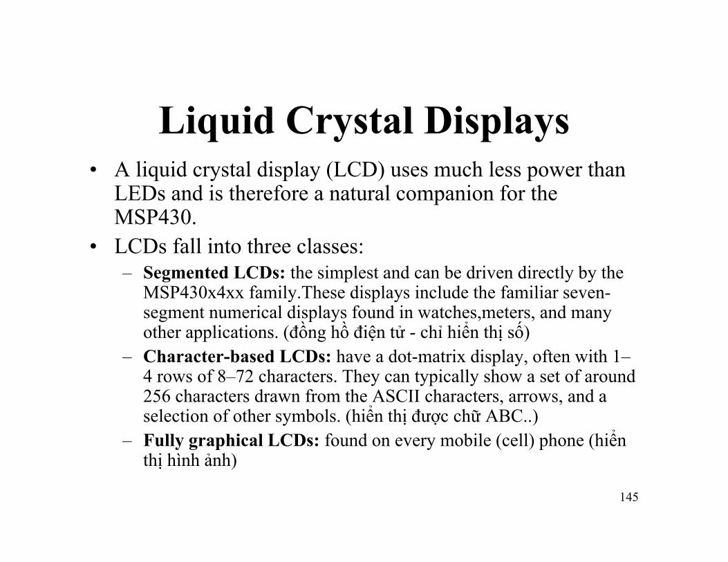
Liquid Crystal Displays• A liquid crystal display (LCD) uses much less power than
LEDs and is therefore a natural companion for the MSP430.
• LCDs fall into three classes:– Segmented LCDs: the simplest and can be driven directly by the
MSP430x4xx family.These displays include the familiar seven-segment numerical displays found in watches,meters, and many other applications. (đồng hồ điện tử - chỉ hiển thị số)
– Character-based LCDs: have a dot-matrix display, often with 1–4 rows of 8–72 characters. They can typically show a set of around 256 characters drawn from the ASCII characters, arrows, and a selection of other symbols. (hiển thị được chữ ABC..)
– Fully graphical LCDs: found on every mobile (cell) phone (hiển thị hình ảnh)

146
147
Driving an LCD from an MSP430x4xx
• All devices in the MSP430x4xx family contain an LCD controller and newer variants have an enhanced version called the LCD_A ( for segmented LCD)– http://www.youtube.com/watch?v=M1wugVxp
9t4&feature=related• Character-based LCDs are usually
incorporated into modules with a “Hitachi” interface.
148
Simple Applications of the LCD
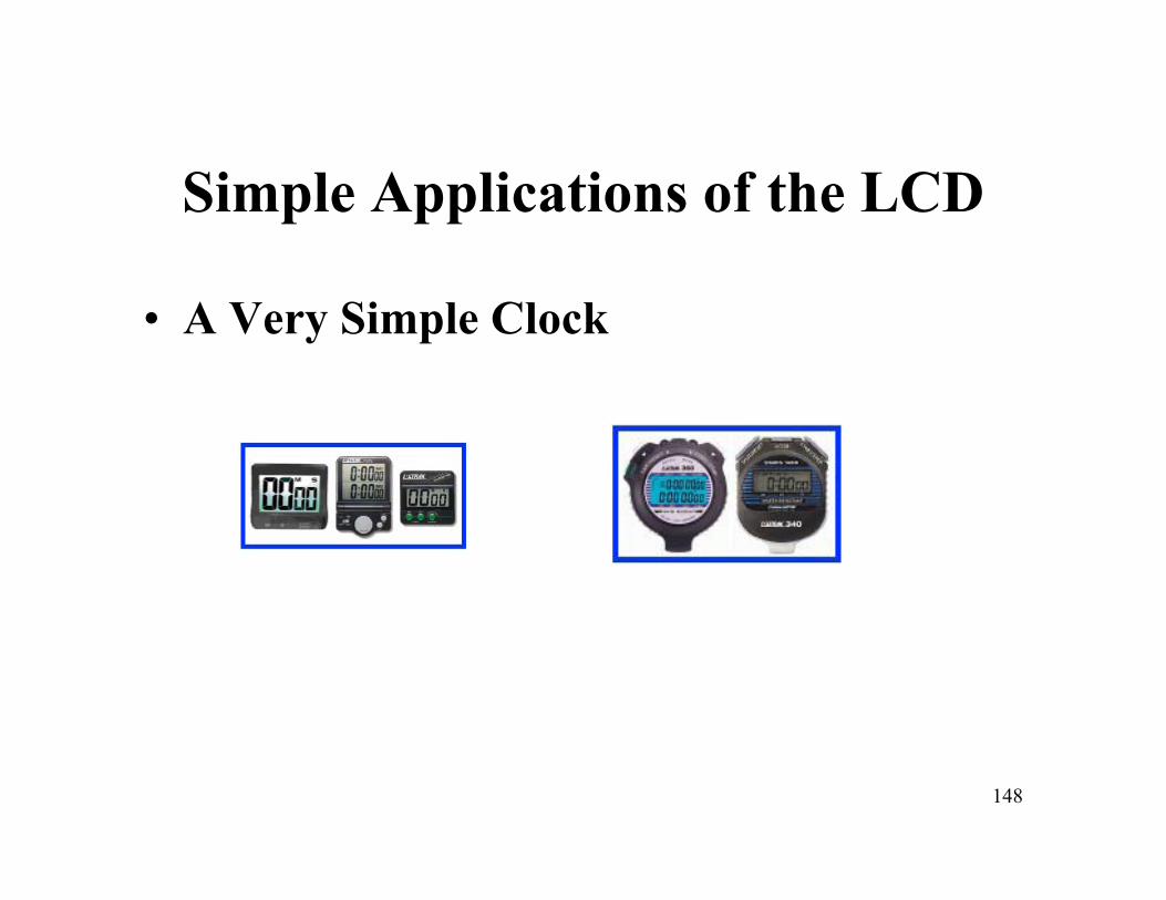
• A Very Simple Clock
149
HD44780 LCD
• 2-rows by 16-character” display, a 3V alphanumeric LCD module (Tianma TM162JCAWG1) compatible with the
• Industry-standard HD44780 controllers

150
151
152
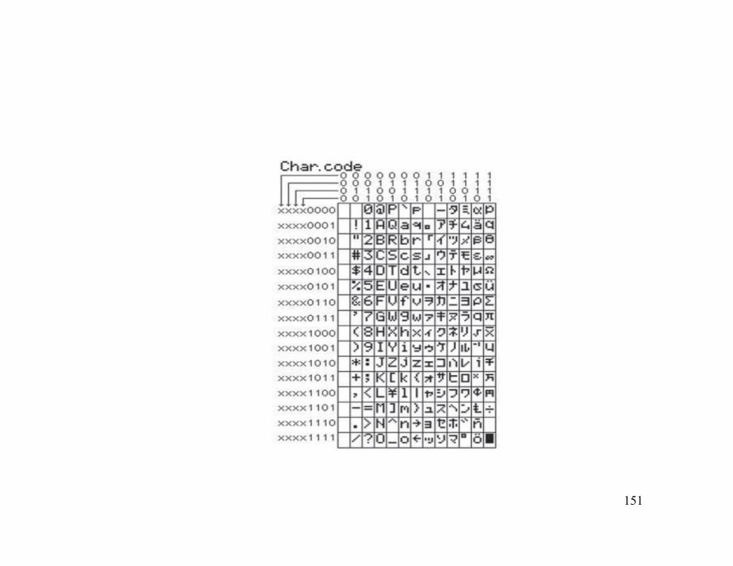
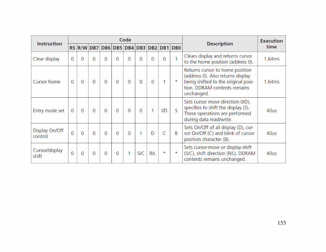
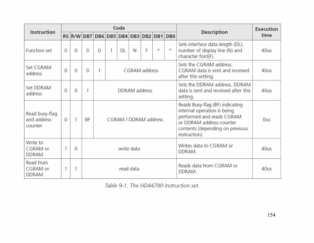
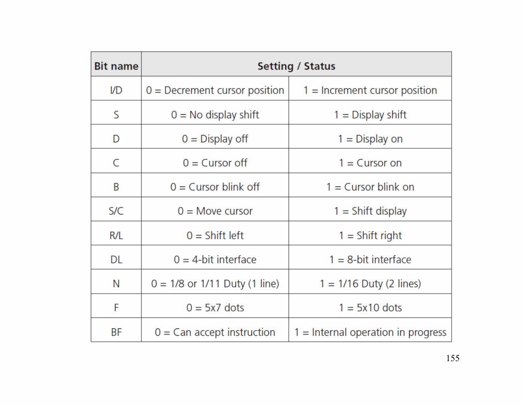
HD44780 controller compatibility
• The HD44780 compatibility means that the integrated controller contains just two registers separately addressable, one for – ASCII data and one for – commands, and the following standard set of
commands can be used to set up and control the display
153
154
155
156
• Demo on youtube• http://www.youtube.com/watch?v=M7dtBx
rTIxA
• Demo on Microcontroller Projects• http://www.circuitvalley.com/2011/12/16x
2-char-lcd-with-ti-msp430-launch-pad.html
157
Chapter 8: Timers1. Watchdog Timer2. Basic Timer1 3. Timer_A 4. Measurement in the Capture Mode5. Output in the Continuous Mode 6. Output in the Up Mode: Edge-Aligned Pulse-Width Modulation 7. Output in the Up/Down Mode: Centered Pulse-Width Modulation 8. Operation of Timer_A in the Sampling Mode 9. Timer_B10. What Timer Where?11. Setting the Real-Time Clock: State Machines
158
159
TimersWatchdog timer: Included in all devices (newer ones have the enhanced watchdog timer+). Its main function is to protect the system against malfunctions but it can instead be used as an interval timer if this protection is not needed.Timer_A: Provided in all devices. It typically has three channels and is much more versatile than the simpler timers just listed. Timer_A can handle external inputs and outputs directly to measure frequency, time-stamp inputs, and drive outputs at precisely specified times, either once or periodicallyTimer_B: Included in larger devices of all families. It is similar to Timer_A with some extensions that make it more suitable for driving outputs such as pulse-width modulation.
160
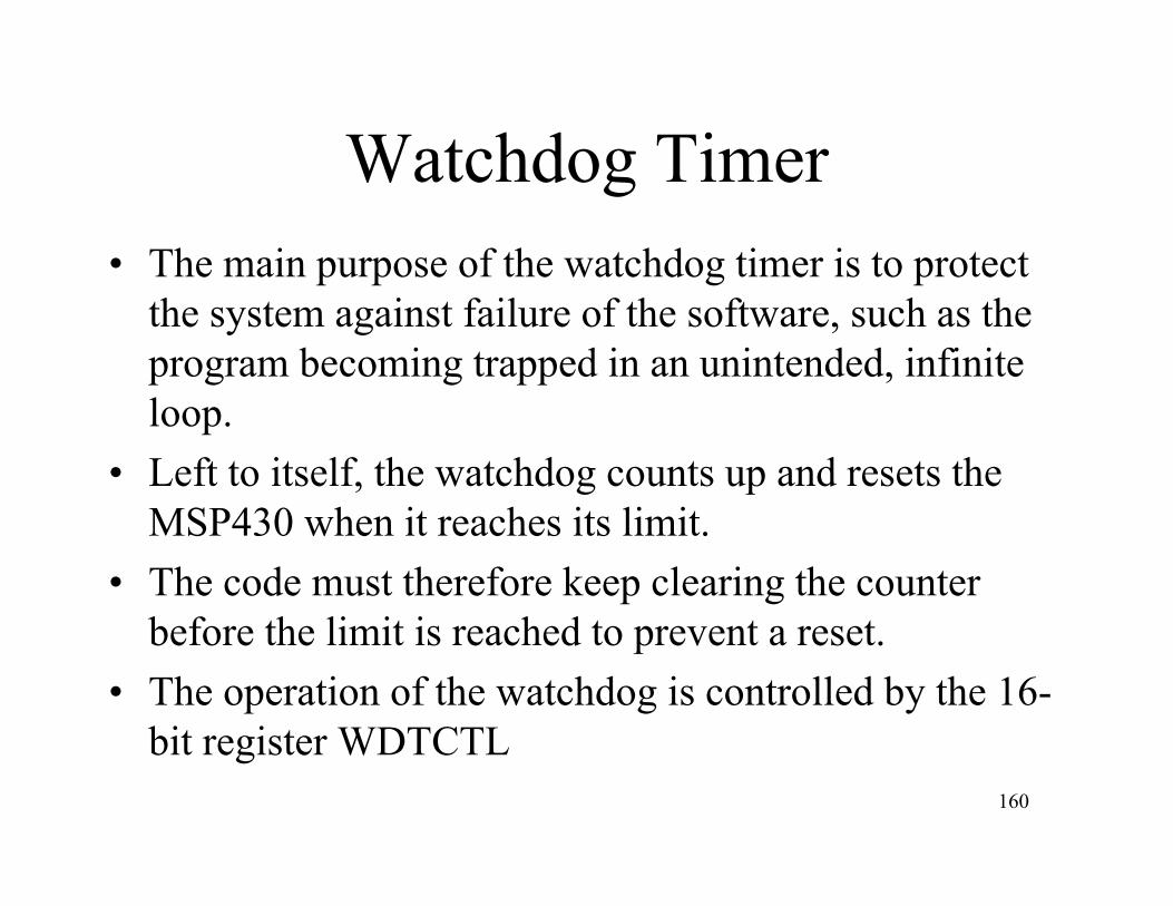
Watchdog Timer• The main purpose of the watchdog timer is to protect
the system against failure of the software, such as the program becoming trapped in an unintended, infinite loop.
• Left to itself, the watchdog counts up and resets the MSP430 when it reaches its limit.
• The code must therefore keep clearing the counter before the limit is reached to prevent a reset.
• The operation of the watchdog is controlled by the 16-bit register WDTCTL
161
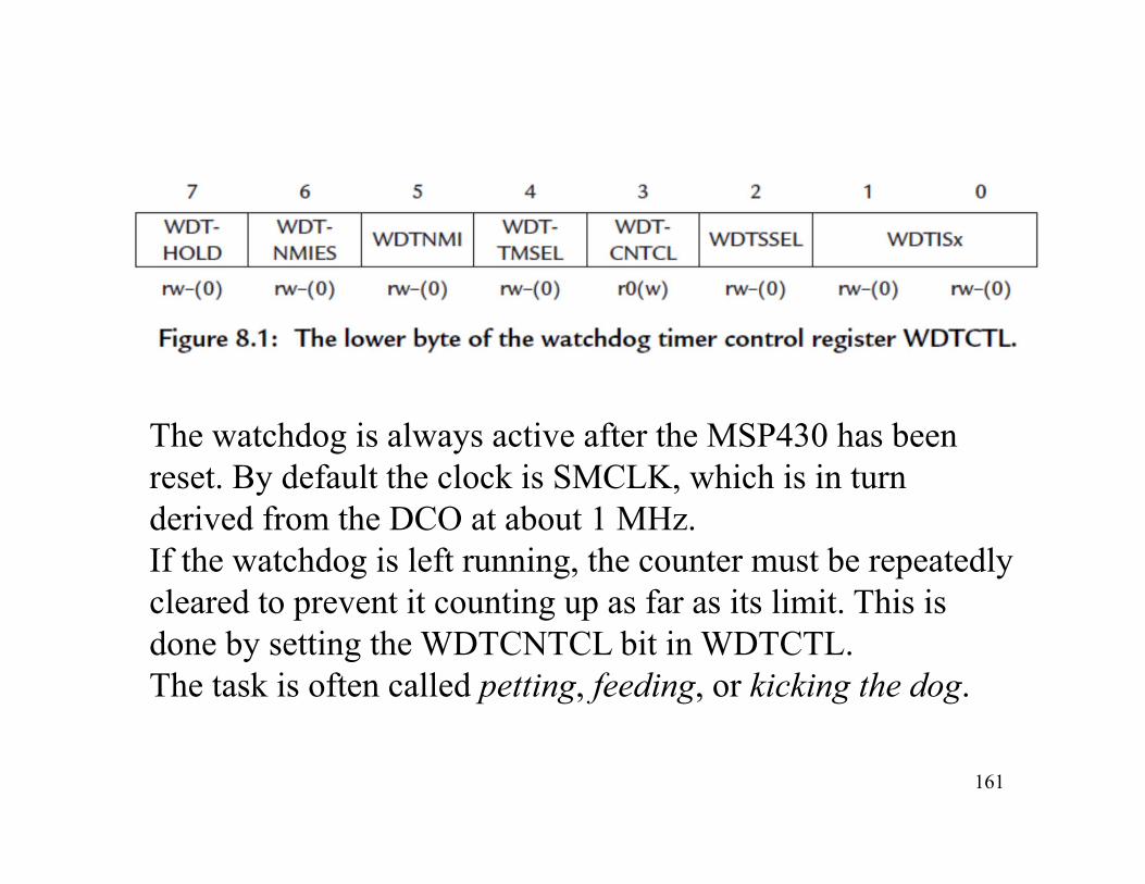
The watchdog is always active after the MSP430 has been reset. By default the clock is SMCLK, which is in turn derived from the DCO at about 1 MHz.If the watchdog is left running, the counter must be repeatedly cleared to prevent it counting up as far as its limit. This is done by setting the WDTCNTCL bit in WDTCTL.The task is often called petting, feeding, or kicking the dog.
162
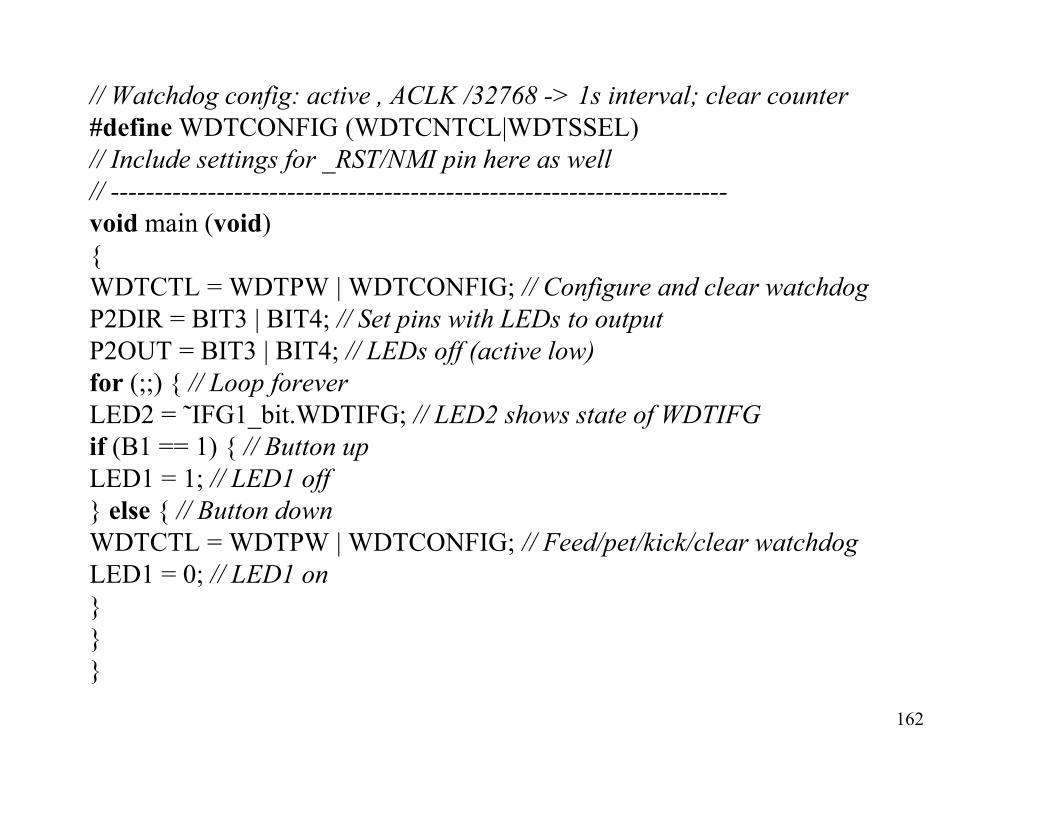
// Watchdog config: active , ACLK /32768 -> 1s interval; clear counter#define WDTCONFIG (WDTCNTCL|WDTSSEL)// Include settings for _RST/NMI pin here as well// ----------------------------------------------------------------------void main (void){WDTCTL = WDTPW | WDTCONFIG; // Configure and clear watchdogP2DIR = BIT3 | BIT4; // Set pins with LEDs to outputP2OUT = BIT3 | BIT4; // LEDs off (active low)for (;;) { // Loop foreverLED2 = ˜IFG1_bit.WDTIFG; // LED2 shows state of WDTIFGif (B1 == 1) { // Button upLED1 = 1; // LED1 off} else { // Button downWDTCTL = WDTPW | WDTCONFIG; // Feed/pet/kick/clear watchdogLED1 = 0; // LED1 on}}}
163
Watchdog as an Interval Timer
• The watchdog can be used as an interval timer if its protective function is not desired.
• Set the WDTTMSEL bit in WDTCTL for interval timer mode.
• The periods are the same as before and again WDTIFG is set when the timer reaches its limit, but no reset occurs.
164
Basic Timer1Basic Timer1 is present in all MSP430xF4xx
165
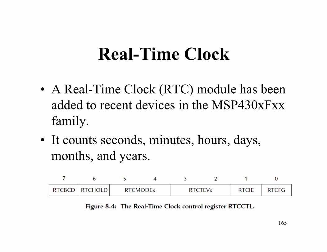
Real-Time Clock
• A Real-Time Clock (RTC) module has been added to recent devices in the MSP430xFxx family.
• It counts seconds, minutes, hours, days, months, and years.
166
Timer_A• This is the most versatile, general-purpose timer in the
MSP430 and is included in alldevices
• Timer block: The core, based on the 16-bit register TAR. There is a choice of sources for the clock, whose frequency can be divided down (prescaled). The timer block has no output but a flag TAIFG is raised when the counter returns to 0.
• Capture/compare channels: In which most events occur, each of which is based on a register TACCRn. They all work in the same way with the important exception of TACCR0.
167
• Capture an input, which means recording the “time” (the value in TAR) at which the input changes in TACCRn; the input can be either external or internal from another peripheral or software.
• Compare the current value of TAR with the value stored in TACCRn and update an output when they match; the output can again be either external or internal.
• Request an interrupt by setting its flag TACCRn CCIFG on either of these events; this can be done even if no output signal is produced.
• Sample an input at a compare event; this special feature is particularly useful if Timer_A is used for serial communication in a device that lacks a dedicated interface.
168
169
• Timer Block (TASSELx bits)– SMCLK is internal and usually fast
(megahertz).– ACLK is internal and usually slow, typically
32 KHz from a watch crystal but may be taken from the VLO in the MSP430F2xx family.
– TACLK is external.– INCLK is also external, sometimes a separate
pin but often it is connected through an inverter to the pin for TACLK so that INCLK = !TACLK.

170
171
Four counter modes• Stop (MC = 0): The timer is halted. All registers,
including TAR, retain their values so that the timer can be restarted later where it left off.
• Continuous (2): The counter runs freely through its full range from 0x0000 to 0xFFFF,at which point it overflows and rolls over back to 0.
• Up (1): The counter counts from 0 up to the value in TACCR0, the capture/compareregister for channel 0. It returns to 0 on the next clock transition.
• Up/Down (3): The counter counts from 0 up to TACCR0, then down again to 0 andrepeats.
172
Capture/Compare Channels
• Timer_A has three channels in most MSP430s although channel 0 is lost to many applications because its register TACCR0 is needed to set the limit of counting in Up and Up/Down modes, as we have just seen.
• Each channel is controlled by a register TACCTLn.
• The central feature of each channel is its capture/compare register TACCRn.
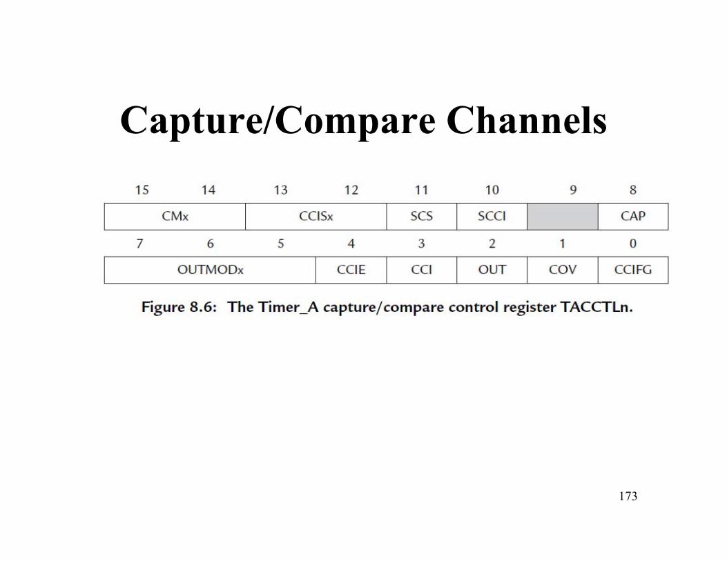
173
Capture/Compare Channels
174
Interrupts from Timer_A
• TACCR0 is privileged and has its own interrupt vector, TIMERA0_VECTOR. Its priority is higher than the other vector, TIMERA1_VECTOR, which is shared by the remaining capture/compare channels and the timer block.
• The MSP430 therefore provides an interrupt vector register TAIV to identify the source of the interrupt rapidly

175
#pragma vector = TIMERA1_VECTOR__interrupt void TIMERA1_ISR (void) // ISR for TACCR1 CCIFG and
TAIFG{// switch (TAIV) { // Standard switchswitch (__even_in_range(TAIV , 10)) { // Faster intrinsic fncase 0: // No interrupt pendingbreak; // No actioncase TAIV_CCIFG1: // Vector 2: CCIFG1P1OUT_bit.P1OUT_0 = 0; // End of duty cycle: Turn off LEDbreak;case TAIV_TAIFG: // Vector A: TAIFG , last value possibleP1OUT_bit.P1OUT_0 = 1; // Start of PWM cycle: Turn on LEDbreak;default: // Should not be possiblefor (;;) { // Disaster. Loop here forever}}}
176
Application of Timers
• Measurement of Time: Reaction Timer• Measurement of Frequency: Comparison of
SMCLK and ACLK• Output in the Continuous Mode
– Generation of Independent, Periodic Signals– A Single Pulse or Delay with a Precise Duration– Generation of a Precise Frequency– Output in the Up Mode: Edge-Aligned– Pulse-Width Modulation

177
Hệ thống nhúng
Ts. Lê Mạnh HảiKhoa CNTT,
ĐH Kỹ thuật Công nghệ TP HCM
Embedded Systems

178
Chapter 10 : Communication
1. Communication Peripherals in the MSP4302. Serial Peripheral Interface3. SPI with the USI4. SPI with the USCI5. Inter-integrated Circuit Bus6. A Simple I²C Master with the USCI_B07. A Simple I²C Slave with the USI on a F2013

179
180
Communication Peripherals in the MSP430
• The universal serial interface (USI) is a lightweight module, which is included in the small F20x2 and F20x3 devices. For a start, it handles only synchronous communication—SPI and I²C.
• Universal Serial Communication Interfacelarger devices in the MSP430F2xx and MSP430F4xx families contain one or more universal serial communication interface (USCI) modules. The hardware handles almost all aspects of the communication, unlike the USI, so the software needs only to provide the data to transmit and store the received data in normal operation. Typically this requires only a couple of small interrupt service routines.• Universal Synchronous/Asynchronous Receiver/Transmitter(USART) is an older module, which has been superseded by the USCI.
181
182
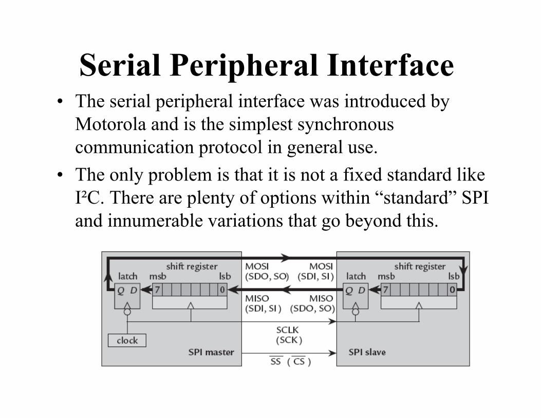
Serial Peripheral Interface• The serial peripheral interface was introduced by
Motorola and is the simplest synchronous communication protocol in general use.
• The only problem is that it is not a fixed standard like I²C. There are plenty of options within “standard” SPI and innumerable variations that go beyond this.
183
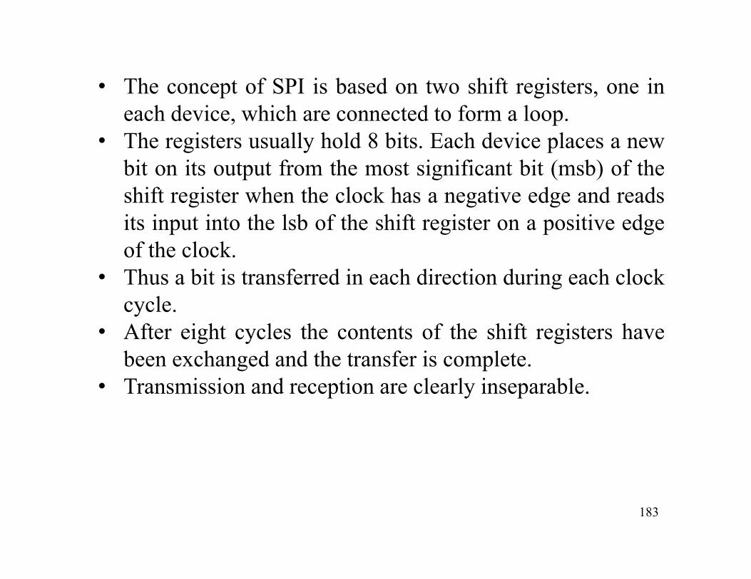
• The concept of SPI is based on two shift registers, one ineach device, which are connected to form a loop.
• The registers usually hold 8 bits. Each device places a newbit on its output from the most significant bit (msb) of theshift register when the clock has a negative edge and readsits input into the lsb of the shift register on a positive edgeof the clock.
• Thus a bit is transferred in each direction during each clockcycle.
• After eight cycles the contents of the shift registers havebeen exchanged and the transfer is complete.
• Transmission and reception are clearly inseparable.
184
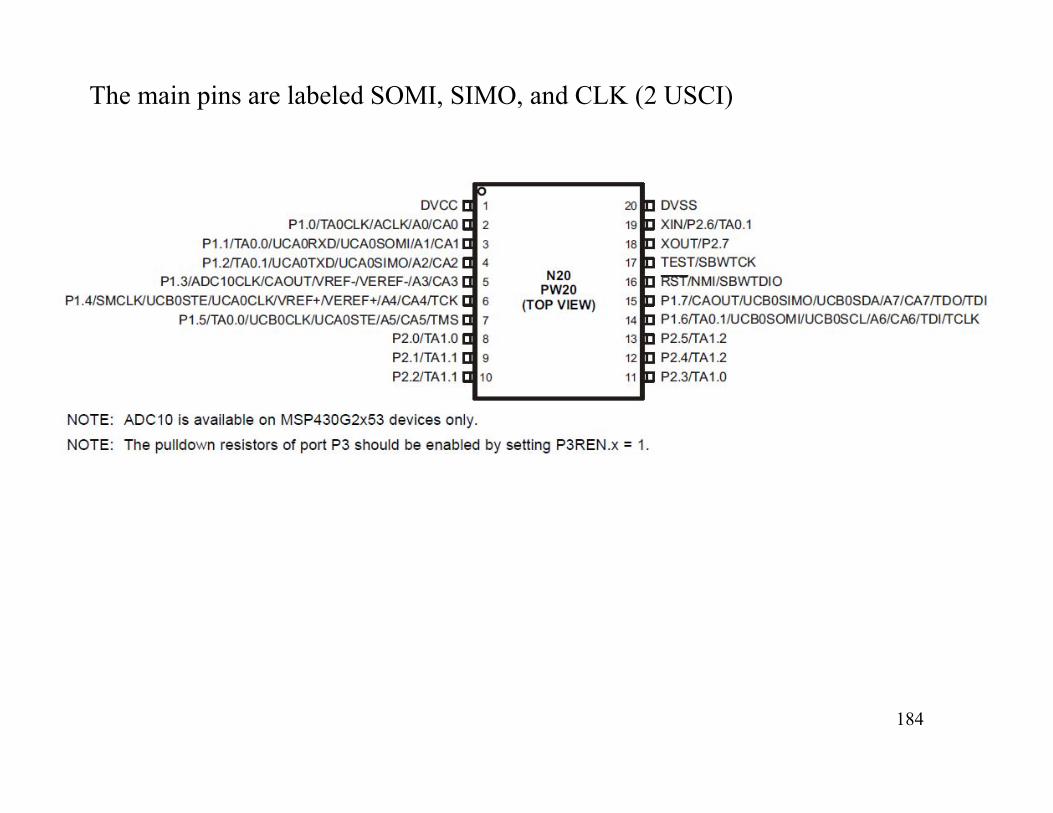
The main pins are labeled SOMI, SIMO, and CLK (2 USCI)
185
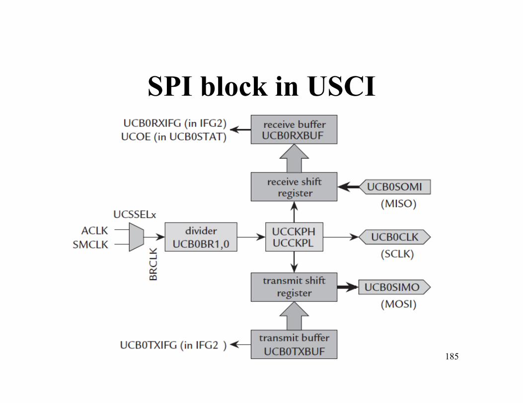
SPI block in USCI
186
SPI operationThere are separate shift registers for transmitting and receivingMoreover, these registers are double-buffered and the user has no direct access to the shift registers themselves. This means that a byte is moved from the receive shift register to RXBUF as soon as reception is complete, which leaves the shift register ready to accept the next transfer. Similarly, a byte written to TXBUF remains in its buffer until the previous byte has been transmitted, at which point it is moved to the transmit shift register. This relaxes considerably the constraints on handling interrupts in the USI, where the shift register must be read and updated rapidly between transfers. Although there are separate registers,reception and transmission are not independent because of the nature of SPI.
187
Read an examples C code for SPI communicationFor Mastermsp430g2xx3_uscia0_spi_09.cAnd for Slavemsp430g2xx3_uscia0_spi_10.c
188
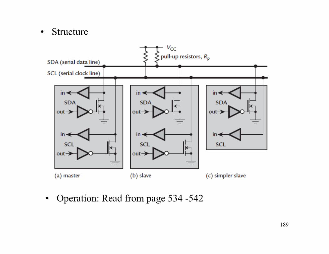
Inter-integrated Circuit Bus• The I²C bus was introduced by Philips (now NXP)
Semiconductors. It was widely adopted and has become even more popular since its patents expired in 2006. It is a true bus, unlike SPI, with a specification and user manual that can be downloaded from NXP.
• Revision 03 of the user manual is document UM10204, dated June 19, 2007. It is clearly written and a lot easier to read than you might expect. The I²C bus uses only two, bidirectional lines:
• Serial data (SDA).• Serial clock (SCL).
189
• Structure
• Operation: Read from page 534 -542

Ôn tập Hệ thống nhúng
1. Cấu trúc tổng thể của vi điều khiển 2. Sơ đồ khối của chíp TI MSP430G25533. Bộ nhớ MSP430G2553: Phân bổ vị trí bộ nhớ và ý
nghĩa từng vùng nhớ 4. Cấu tạo CPU và ý nghĩa các thanh ghi trong CPU5. Các loại xung nhịp (clock) và các chế độ hoạt động6. Hàm và các bước thực hiện khi gọi một hàm7. Khái niệm ngắt và chương trình phục vụ ngắt8. Các bước thực thi khi thực hiện một ngắt. 9. Các chế độ công suất thấp.10. Các cổng nhập xuất số (Digital Input and Output).11. Quét ma trận bàn phím. Chống dội 12. Các loại LCD. Sơ đồ chân kết nối theo chuẩn
HD44780 13. Các loại timer. Cấu trúc và hoạt động của WDT14. Cấu trúc và các chế độ hoạt động của TimerA015. Kết nối Serial Peripheral Interface (SPI). Cấu trúc
và hoạt động.16. Kết nối Inter-integrated Circuit Bus (I2C).