finfet design
TRANSCRIPT

FinFET Design Using Sentaurus
TCAD Tool

Sentaurus TCAD 2014
2
FinFET Design Using Sentaurus
TCAD Tool
By
Mr. Sanjeet D. Sawant
Report submitted after completion of Internship
At Systems Engineering Lab of CeNSE
Indian Institute of Science, Bangalore
20th
May, 2014
Under the guidance of
Dr. Vijay Mishra Mr Kiran GK
Technology Manager, Facility Technologist,
CeNSE, IISc, Bangalore CeNSE, IISc, Bangalore
Sentaurus TCAD 2014
3
Acknowledgements
The Internship was carried out under the able guidance of Dr. Vijay Mishra,
Technology Manager, CeNSE, IISc, Bangalore. I would like to sincerely thank him
for giving me the opportunity to work under him for the project. I would like to
place on record my thanks to Mr. Kiran GK for their constant support and technical
guidance throughout the project. I would be failing in my duty, if I do not express
my heartfelt gratitude to all the members of Systems Lab for their encouragement
and support during this period.
Sanjeet Sawant

Sentaurus TCAD 2014
4
Abstract
FinFETs are of various types like SOI FinFET, BOI FinFET, Bulk FinFET,
etc. Here we will be having an over-view on designing of BOI FinFET using
Sentaurus TCAD Tool . TCAD consists of two main branches: process
simulation and device simulation. Fabrication processes like Depositing of
materials like Silicon, Polysilicon Oxide, etc. , Etching , Implantation of ion,
etc. come under process simulation . After the fabrication process it will be
gone under contact allocation for device simulation to see the characteristics
of the device process.

Sentaurus TCAD 2014
5
Contents Page
Section........................................................................Page Number
1. Introduction.............................................................................6
2. Objectives................................................................................7
3. Background Work...................................................................8
4. Sentaurus process(sprocess)............................................9
5. Sentaurus device(sdevice)............................................21
6. Inspect.................................................................................... 27
7. Sentaurus Workbench........................................................ 28
8. Conclusion..................................................................................29
9. Biblography.................................................................................30

Sentaurus TCAD 2014
6
Introduction
Sentaurus TCAD tool is a tool used for simulation and also to solve
fundamental, physical, partial differential equations, such as diffusion and
transport equations for discretized geometries, representing the silicon wafer
or the layer system in a semiconductor device.
TCAD computer simulations substitute for costly and time-consuming test
wafer runs when developing and characterizing a new semiconductor device
or technology.
TCAD tool is widely used in Semiconductor Industry.
As technologies become more complex, the semiconductor industry relies
increasingly more on TCAD to cut costs and speed up the research and
development process. In addition, semiconductor manufacturers use TCAD
for yield analysis, that is, monitoring, analyzing, and optimizing their IC
process flows, as well as analyzing the impact of IC process variation.
TCAD consists of two main branches: process simulation and device
simulation.

Sentaurus TCAD 2014
7
Objectives
The objective of the project was to design BOI FinFET and study the
characteristics of the device designed which included various steps.
This includes various steps required for designing and simulation:
1. Sentaurus process (sprocess )
In sprocess through TCL (Techinical Command Language) we can create
structure of any semiconductor device.
2. Sentaurus device (sdevice)
Sentaurus Device simulates the electrical, thermal, and optical
characteristics of semiconductor devices.
3. Inspect
Inspect is a plotting and analysis tool for xy data such as doping profiles and
electrical characteristics of semiconductor devices.
4. Sentaurus Workbench
Sentaurus Workbench is Graphical User Interface (GUI) used to design,
organize, and run simulations for semiconductor research and
manufacturing. It automatically manages the information flow from one tool
to another which includes preprocessing user input files, parameterizing
projects, setting up and executing tool instances, and visualizing the results.

Sentaurus TCAD 2014
8
Background Work
Understanding the fabrication process of the transistor layer by layer especially
processes like depositing, etching, implantation, doping, etc. which will be used in
sprocess.
In sdevice we will need to give the inputs for Gate length, Work functions, Gate
voltage, Drain voltage, etc.
Basically we need to know the device geometry, doping concentration, material
used for depositing, Gate length and the input voltage and current of the
semiconductor device.

Sentaurus TCAD 2014
9
Sentaurus process (sprocess)
Overview:
Sentaurus Process is a complete and highly flexible multidimensional
process modeling environment. With its modern software architecture, it
constitutes a new-generation tool and a solid base for process simulation.
Calibrated to a wide range of the latest experimental data using proven
calibration methodology, Sentaurus Process offers unique predictive
capabilities for modern silicon and nonsilicon technologies.
File types:
Sentaurus Process command file (*.cmd)
This is the main input file type for Sentaurus Process. It contains all
the process steps and can be edited. This file is referred to as the command
file or input file.
Log file (*.log)
Sentaurus Process generates this file during a run. It contains information
about each process step, and the models and values of physical parameters
used in it.
TDR boundary file (*_bnd.tdr)
This Synopsys-specific format stores the geometry of the device and is
usually saved by users at the end of a simulation. This file is used as the
input file for Sentaurus Visual for viewing.
To open a TDR file, open a terminal window and launch the TDR file
viewer with the command:
svisual <file_name>.tdr

Sentaurus TCAD 2014
10
3 Dimensional BOI FinFET Process Simulation :
Initially we need to define the 3D grid for the FinFET
The initial 3D grid is defined with the line command:
# X lines
line x location= 0.0 spacing=0.01<um> tag=back
line x location= 0.15<um> spacing=0.01<um> tag=front
# Y lines
line y location=0.0 spacing=0.01<um> tag=Left
line y location=0.15<um> spacing=0.01<um> tag=Right
# Z lines
line z location= 0.0 spacing=0.01<um> tag=SiBottom
line z location=0.21<um> spacing=0.01<um> tag=SiTop
Sentaurus Process uses coordinate systems such that 2D
and 3D simulations are consistent.
Above commands create a base structure of the substrate Silicon
Defining Simulation Domain and Initialization
The initial simulation domain is defined with the region command:
region silicon xlo=back xhi=front ylo=Left yhi=Right /
zlo=SiBottom zhi=SiTop
init wafer.orient=100 field=Boron concentration=2e15
For a 3D simulation, the substrate region is defined by referring to
the tag for the x-direction, y-direction and z-direction. These tags
were defined in the line command above .

Sentaurus TCAD 2014
11
Here, an n-doped substrate with a Boron concentration of 2x10¹⁵
cm-3
is used. The wafer orientation is set to be (100), which is the default.
Silicon substrate formation
The Silicon substrate is created using :
# Silicon
#-----------------------------------------------------------------
mask name=sili left= 0.0<um> right= 0.1<um> back=0.0<um>
front= 0.3<um>
etch material= {Silicon} type=anisotropic time=1 rate= {0.01}
mask=sili
mask name=sili1 left= 0.1<um> right= 0.2<um> back=0.0<um>
front=0.3<um>
etch material= {Silicon} type=anisotropic time=1 rate= {0.01}
mask=sili1
struct tdr.bnd= Silicon
First, A mask is defined to protect the Silicon area with the mask
command. In this project, only half of the transistor is simulated. The
left edge of the gate mask is, therefore, unimportant.
0.01 μm ( rate= {0.01} of Silicon is etched over the entire structure
except the masked area. The keyword type=anisotropic means that
the layer is grown in the vertical direction only.
The first etch command refers to the previously defined mask and,
therefore, only the exposed part of the Silicon is etched. Note that the
requested etching depth is larger than the deposited layer. This over
etching ensures that no residual islands remain. The etching is
specified to be anisotropic, that is, the applied mask is transferred
straight down, without any undercut.

Sentaurus TCAD 2014
12
struct tdr.bnd= Silicon creates geometry of the device after the
simulation of the command which can give the proper visual idea of
the device.
Figure 1

Sentaurus TCAD 2014
13
LOCOS process
LOCOS, short for Local Oxidation of Silicon, is a micro
fabrication process where silicon dioxide is formed in selected areas
on a silicon wafer having the Si-SiO2 interface at a lower point than
the rest of the silicon surface.
There are 4 basic layers:
1: Si, Silicon substrate, wafer
2:SiO2, chemical vapour deposition of silicon oxide
3: Si3N4
4:SiO2, insulation oxide, thermal oxidation
Line command for LOCOS process:
# LOCOS
#-----------------------------------------------------------------
deposit material= {SiO2} type=anisotropic time=1 rate= {0.003}
struct tdr.bnd= SiO2
deposit material= {Si3N4} type=anisotropic time=1 rate= {0.005}
struct tdr.bnd= Si3N4
deposit material= {Polysilicon} type=anisotropic time=1 rate=
{0.007}
struct tdr.bnd= Poly
mask name=pol left= 0.0<um> right= 0.08<um> back=0.0<um>
front= 0.02<um>
etch material= {Polysilicon} type=anisotropic time=1 rate=
{0.008} mask=pol
struct tdr.bnd= Pol

Sentaurus TCAD 2014
14
Figure 2
Arsenic implantation
Command line for Arsenic implantation:
# Arsenic implantation
# ------------------------------------------------------------
deposit material= {SiO2} type=anisotropic time=1 rate= {0.07}
mask name=ox left= 0.0<um> right= 0.08<um> back=0.0<um>
front= 0.02<um>
etch material= {SiO2} type=anisotropic time=1 rate= {0.08}
mask=ox
etch material= {SiO2} type=anisotropic time=1 rate= {0.04}
implant arsenic energy=5 dose=1e15 tilt=0 rotation=0
struct tdr.bnd= As

Sentaurus TCAD 2014
15
The Arsenic implantation uses a high dose of 1014
cm-2
and a
relatively low energy of 5eV.
Fin formation
Command line for Fin formation:
#Fin formation
#-----------------------------------------------------
mask name=fin left= 0.07<um> right= 0.2<um> back=0.0<um>
front= 0.25<um>
etch material= {Si3N4} type=anisotropic time=1 rate= {0.007}
mask=fin
etch material= {SiO2} type=anisotropic time=1 rate= {0.004}
mask=fin
etch material= {SiO2} type=anisotropic time=1 rate= {0.03}
etch material= {Polysilicon} type=anisotropic time=1 rate=
{0.009}
mask name=fin1 left= 0.0<um> right= 0.2<um> back=0.01<um>
front= 0.25<um>
deposit material= {SiO2} type=anisotropic time=1 rate= {0.03}
mask=fin1
mask name=fin2 left= 0.07<um> right= 0.2<um> back=0.0<um>
front= 0.25<um>
etch material= {Si3N4} type=anisotropic time=1 rate= {0.006}
mask=fin2
etch material= {SiO2} type=anisotropic time=1 rate= {0.003}
mask=fin2
etch material= {SiO2} type=anisotropic time=1 rate= {0.03}
etch material= {Silicon} type=anisotropic time=1 rate= {0.03}
struct tdr.bnd= fin

Sentaurus TCAD 2014
16
Figure 3
mask name=fin3 left= 0.0<um> right= 0.07<um>
back=0.01<um> front= 0.25<um>
deposit material= {Silicon} type=anisotropic time=1 rate= {0.02}
mask=fin3
etch material= {Silicon} type=anisotropic time=1 rate= {0.02}
mask name=fin4 left= 0.0<um> right= 0.063<um>
back=0.017<um> front= 0.25<um>
deposit material= {Silicon} type=anisotropic time=1 rate= {0.025}
mask=fin4
mask name=fin5 left= 0.0<um> right= 0.07<um>
back=0.01<um> front= 0.25<um>
etch material= {Silicon} type=anisotropic time=1 rate= {0.025}
mask=fin5
deposit material= {Si3N4} type=anisotropic time=1 rate= {0.033}
mask=fin4
etch material= {Si3N4} type=anisotropic time=1 rate= {0.033}
mask=fin5
etch material= {Si3N4} type=anisotropic time=1 rate= {0.033}
deposit material= {Silicon} type=anisotropic time=1 rate= {0.025}
mask=fin5

Sentaurus TCAD 2014
17
etch material= {Silicon} type=anisotropic time=1 rate= {0.025}
mask=fin4
deposit material= {SiO2} type=anisotropic time=1 rate= {0.025}
mask=fin4
etch material= {SiO2} type=anisotropic time=1 rate= {0.025}
mask=fin5
deposit material= {Si3N4} type=anisotropic time=1 rate= {0.033}
mask=fin4
etch material= {Si3N4} type=anisotropic time=1 rate= {0.028}
mask=fin5
etch material= {Si3N4} type=anisotropic time=1 rate= {0.033}
mask name=fin6 left= 0.0<um> right=0.067<um> back=0.0<um>
front=0.25<um>
deposit material= {Oxide} type=anisotropic time=1 rate= {0.025}
mask=fin6
mask name=fin7 left= 0.0<um> right= 0.07<um> back=0.0<um>
front= 0.25<um>
etch material= {Oxide} type=anisotropic time=1 rate= {0.025}
mask= fin7
mask name=fin8 left=0.0<um> right=0.15<um> back=0.01<um>
front= 0.25<um>
etch material= {Oxide} type= anisotropic time=1 rate= {0.03}
mask= fin8
deposit material= {Oxide} type=anisotropic time=1 rate= {0.003}
mask=fin8
struct tdr.bnd= fin13

Sentaurus TCAD 2014
18
Figure 4
Polysilicon Gate formation:
Command line for Polysilicon Gate formation:
#Polysilicon Gate
#-----------------------------------------------------------------
mask name=gate left=0.07<um> right=0.15<um> back=0.0<um>
front= 0.25<um>
deposit material= {Polysilicon} type= anisotropic time=1 rate=
{0.08} mask=gate
mask name=gate1 left=0.0<um> right=0.063<um>
back=0.017<um> front= 0.25<um>
etch material= {Polysilicon} type= anisotropic time=1 rate= {0.025}
mask= gate1
mask name=gate2 left=0.0<um> right=0.067<um> back=0.01<um>
front= 0.25<um>

Sentaurus TCAD 2014
19
etch material= {Polysilicon} type= anisotropic time=1 rate= {0.025}
mask= gate2
mask name=gate3 left=0.0<um> right=0.15<um> back=0.01<um>
front= 0.25<um>
etch material= {Polysilicon} type= anisotropic time=1 rate= {0.003}
mask= gate3
mask name=gate4 left=0.065<um> right=0.15<um> back=0.0<um>
front= 0.25<um>
Figure 5

Sentaurus TCAD 2014
20
Phosphorus implantation
Command line for phosphorus implantation:
implant phosphorus energy=0.6 dose=1e15 tilt=0 rotation=0
mask=gate4
struct tdr= phos
Figure 6
Sentaurus TCAD 2014
21
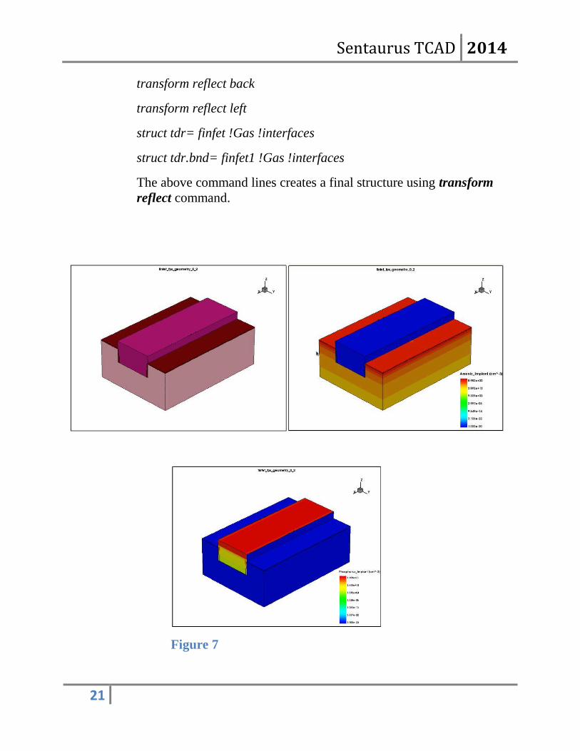
transform reflect back
transform reflect left
struct tdr= finfet !Gas !interfaces
struct tdr.bnd= finfet1 !Gas !interfaces
The above command lines creates a final structure using transform
reflect command.
Figure 7

Sentaurus TCAD 2014
22
Sentaurus device (sdevice)
Overview:
Sentaurus Device is a numeric semiconductor device simulator,
capable of simulating the electrical, thermal, and optical characteristics
of various semiconductor devices.
It simulates 1D, 2D, and 3D device behavior over a wide range of
operating conditions, including mixed-mode circuit simulation,
combining numerically simulated devices with their compact modeling,
which is performed on a SPICE-based circuit simulation level.
Command File
A typical command file of Sentaurus Device consists of several
command sections ,with each section executing a relatively
independent function. The default extension of the command file is
_des.cmd For example, pp1_des.cmd
The command file typically contains the following:
1: File section
2: Electrode section
3: Physics section
4: Plot section
5: Math section
6: Solve section
File Section
The File section defines the input and output files of the simulation,
such as:
File {
* Input Files
Grid = "nmos_msh.tdr"
Parameter = "nmos.par"

Sentaurus TCAD 2014
23
* Output Files
Current = "nmos"
Plot = "nmos"
Output = "nmos"
}
Input files(.tdr , .par):
Sentaurus Device expects at least one input file to define the device
structure and the field values, which are mandatory doping-profile
distributions and the optional mechanical-stress distribution inside a
device.
The grid file can represent 1D, 2D, or 3D device dimensions. It is
typically generated by the mesh engine Sentaurus Mesh. The file
extension .tdr indicates that the file is in TDR format, which is the
default format produced by Sentaurus Mesh.
The optional Parameter file includes the specifications of the
material parameters and user-defined model parameters. Parameter
values specified in this file supersede the Sentaurus Device built-in
defaults. The common extension used for Sentaurus Device
parameter files is .par.
Output files:
Sentaurus Device produces several output files:
1:A file containing electrode names and resulting voltages,
currents, charges, times, temperatures, and so on, whose name is
indicated in the Current statement
2:A file with the spatially distributed solution variables and their
derivatives, whose name is indicated in the Plot statement
3:A protocol file whose name is indicated in the Output
statement

Sentaurus TCAD 2014
24
Figure 8 Flow of input and output files in Sentaurus
Device.
The Output file specification instructs Sentaurus Device where to put
the output generated during the device simulation. Sentaurus Device
always adds the extension _des.log to the actual file name.
Electrode Section:
The electrical device contacts are declared in the Electrode section
together with the initial boundary conditions (bias) and other
optional specifications.
Each electrode defined here must match exactly (case sensitive) an
existing contact name in the Grid file. Only the contacts named in
the Electrode section are included in the simulation.
Example for electrode specification:
Electrode {
{ Name="Source" Voltage= 0.0 }
{ Name="Drain" Voltage= 1.5V }
{ Name="Gate" Voltage= 1.5V Workfunction=@Work@ }

Sentaurus TCAD 2014
25
By default, Sentaurus Device treats an electrode as an ideal Ohmic
contact, where the charge neutrality and equilibrium are assumed
for the source contact.
The electrodes are allocated in the sprocess command file by
defining the contacts. Command for defining contacts is given
below.
#Contact
#----------------------------------------------------------------------
contact name= gate box PolySilicon \
xlo=-0.25 xhi=0.25 ylo=-0.07 yhi=0.07 zlo=0.14 zhi=0.17
contact name=source box Silicon \
xlo=-0.25 xhi=0.25 ylo=0.07 yhi=0.15 zlo=0.1 zhi=0.15
contact name= drain box Silicon \
xlo=-0.25 xhi=0.25 ylo=-0.15 yhi=0.07 zlo=0.1 zhi=0.15
contact name= substrate bottom
Physics Section
In the Physics section, you declare the physical models to be used in
the simulation. The physical models can be defined globally:
Physics { [list of models] }
or materialwise:
Physics (Material="[material name]") {
[list of models]
}
or regionwise:
Physics (RegionInterface="[region name]") {
[list of models]
}
Specifying physical models globally means that the included
models are valid for all device regions. With a qualifier such as

Sentaurus TCAD 2014
26
Material="[material name]" or RegionInterface="[region name]", the
specified models are activated only in the designated material or
regions.
Plot Section
The Plot section is used to specify the variables to be saved in the Plot
file (named in the File section) for further visualization in Sentaurus Visual:
Plot {
[list of variables]
}
The plot is performed at the end of the simulation or along the
electrode boundary-condition sweep, by having a Plot command specified
within the Solve section.
Math Section
The Math section is used to control the simulator numerics.
Solve Section
The Solve section consists of a series of simulation commands to
be performed that are activated sequentially. The specified command
sequence instructs the simulator as to which task must be solved and
how.
Sentaurus TCAD 2014
27
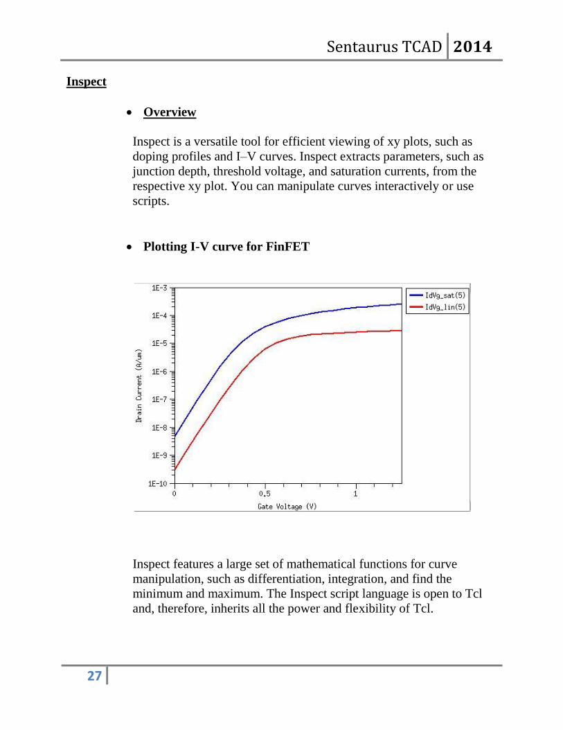
Inspect
Overview
Inspect is a versatile tool for efficient viewing of xy plots, such as
doping profiles and I–V curves. Inspect extracts parameters, such as
junction depth, threshold voltage, and saturation currents, from the
respective xy plot. You can manipulate curves interactively or use
scripts.
Plotting I-V curve for FinFET
Inspect features a large set of mathematical functions for curve
manipulation, such as differentiation, integration, and find the
minimum and maximum. The Inspect script language is open to Tcl
and, therefore, inherits all the power and flexibility of Tcl.

Sentaurus TCAD 2014
28
Sentaurus Workbench
Overview :
Sentaurus Workbench is the primary graphical front end that
integrates TCAD Sentaurus simulation tools into one environment.
It is used throughout the semiconductor industry to design,
organize, and run simulations.
Simulations are organized comprehensively into projects. Sentaurus
Workbench automatically manages the information flow, which
includes preprocessing user input files, parameterizing projects,
setting up and executing tool instances, and visualizing results.
Sentaurus Workbench allows you to define parameters and variables
to run comprehensive parametric analyses. The resulting data can be
used with statistical and spreadsheet tools.
Sentaurus TCAD 2014
29
Conclusion:
The internship work relates to studying the Sentaurus TCAD software and the
tools used for transistor designing. The main aim was to design a BOI FinFET in
Sentaurus TCAD which has been successfully done. The structure of the BOI
FinFET is created using TCL language in Sentaurus process. The contact are
defined for the Electrode section in Sentaurus device for device simulation. The
simulation was carried out in Sentaurus Workbench. The I-V characteristics are
being inspected.

Sentaurus TCAD 2014
30
Bibliography
1. Introduction to VLSI Circuits and Systems – Dr. John P. Uyemura
2. High-Performance BOI FinFETs Based on Bulk-Silicon Substrate -
Xiaoyan Xu, Runsheng Wang, Student Member, IEEE, Ru Huang, Senior
Member, IEEE, Jing Zhuge, Student Member, IEEE, Gang Chen, Xing
Zhang, Member, IEEE, and Yangyuan Wang, Fellow, IEEE
3. Highly Manufacturable Double-Gate FinFET With Gate-Source/Drain
Underlap - Ji-Woon Yang, Member, IEEE, Peter M. Zeitzoff, Member, IEEE,
and Hsing-Huang Tseng, Senior Member, IEEE