kodak kai-2020 kodak kai-2020m kodak kai … · kai-2020 rev. 2.1 585-722-4385 email:...
TRANSCRIPT
K A I - 2 0 2 0 R e v . 2 . 1 w w w . k o d a k . c o m / g o / i m a g e r s 5 8 5 - 7 2 2 - 4 3 8 5 E m a i l : i m a g e r s @ k o d a k . c o m
IMAGE SENSOR SOLUTIONS
D E V I C E P E R F O R M A N C E S P E C I F I C A T I O N
KODAK KAI-2020 KODAK KAI-2020M KODAK KAI-2020CM Image Sensor 1600 (H) x 1200 (V) Interline Transfer Progressive Scan CCD
July 6, 2005 Revision 2.1
K A I - 2 0 2 0 R e v . 2 . 1 w w w . k o d a k . c o m / g o / i m a g e r s 5 8 5 - 7 2 2 - 4 3 8 5 E m a i l : i m a g e r s @ k o d a k . c o m
IMAGE SENSOR SOLUTIONS
2
TABLE OF CONTENTS
TABLE OF FIGURES................................................................................................................................... 4
DEVICE DESCRIPTION............................................................................................................................... 6 ARCHITECTURE .......................................................................................................................................... 6 OVERALL.................................................................................................................................................... 6
Pixel ..................................................................................................................................................... 7 Vertical to Horizontal Transfer ............................................................................................................. 8 Horizontal Register to Floating Diffusion ............................................................................................. 9 Horizontal Register Split .................................................................................................................... 10 Single Output Operation .................................................................................................................... 10 Dual Output Operation....................................................................................................................... 10 Output ................................................................................................................................................ 11
PHYSICAL DESCRIPTION............................................................................................................................ 14 Pin Description and Device Orientation ............................................................................................. 14
PERFORMANCE........................................................................................................................................ 15 POWER - ESTIMATED ................................................................................................................................ 15 FRAME RATES .......................................................................................................................................... 15 IMAGING PERFORMANCE ........................................................................................................................... 16
Image Performance Operational Conditions...................................................................................... 16 Imaging Performance Specifications ................................................................................................. 16 Defect Definitions............................................................................................................................... 19 Defect Map......................................................................................................................................... 19 Quantum Efficiency............................................................................................................................ 20 Angular Quantum Efficiency .............................................................................................................. 21 Dark Current versus Temperature ..................................................................................................... 22
TEST DEFINITIONS................................................................................................................................... 23 TEST REGIONS OF INTEREST..................................................................................................................... 23 OVERCLOCKING ....................................................................................................................................... 23
Tests .................................................................................................................................................. 24 OPERATION .............................................................................................................................................. 27
MAXIMUM RATINGS................................................................................................................................... 27 MAXIMUM VOLTAGE RATINGS BETWEEN PINS ............................................................................................ 27 DC BIAS OPERATING CONDITIONS (FOR < 40,000 ELECTRONS) ................................................................. 28 AC OPERATING CONDITIONS .................................................................................................................... 28
Clock Levels....................................................................................................................................... 28 Clock Line Capacitances ................................................................................................................... 29
TIMING REQUIREMENTS ............................................................................................................................ 30 TIMING MODES......................................................................................................................................... 31
Progressive Scan............................................................................................................................... 31 FRAME TIMING.......................................................................................................................................... 32
Frame Timing without Binning - Progressive Scan............................................................................ 32 Frame Timing for Vertical Binning by 2 - Progressive Scan.............................................................. 32 Frame Timing Edge Alignment .......................................................................................................... 33
LINE TIMING ............................................................................................................................................. 34 Line Timing Single Output – Progressive Scan ................................................................................. 34 Line Timing Dual Output – Progressive Scan.................................................................................... 34 Line Timing Vertical Binning by 2 – Progressive Scan ...................................................................... 35 Line Timing Detail – Progressive Scan.............................................................................................. 36 Line Timing Binning by 2 Detail – Progressive Scan......................................................................... 36
K A I - 2 0 2 0 R e v . 2 . 1 w w w . k o d a k . c o m / g o / i m a g e r s 5 8 5 - 7 2 2 - 4 3 8 5 E m a i l : i m a g e r s @ k o d a k . c o m
IMAGE SENSOR SOLUTIONS
3
Line Timing Edge Alignment.............................................................................................................. 37 PIXEL TIMING ........................................................................................................................................... 38
Pixel Timing Detail ............................................................................................................................. 38 FAST LINE DUMP TIMING........................................................................................................................... 39 ELECTRONIC SHUTTER ............................................................................................................................. 40
Electronic Shutter Line Timing........................................................................................................... 40 Electronic Shutter – Integration Time Definition ................................................................................ 40 Electronic Shutter Description ........................................................................................................... 41
LARGE SIGNAL OUTPUT ............................................................................................................................ 41 STORAGE AND HANDLING..................................................................................................................... 42
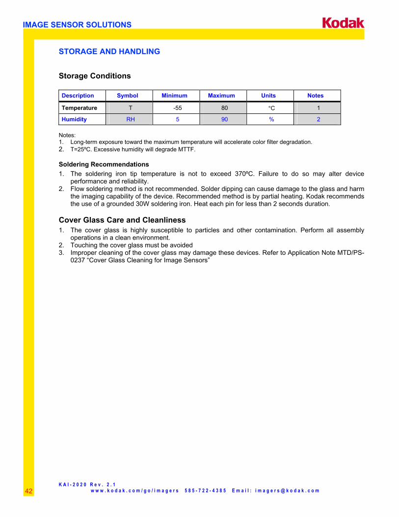
STORAGE CONDITIONS ............................................................................................................................. 42 SOLDERING RECOMMENDATIONS............................................................................................................... 42 COVER GLASS CARE AND CLEANLINESS .................................................................................................... 42
MECHANICAL DRAWINGS ...................................................................................................................... 43 PACKAGE ................................................................................................................................................. 43 DIE TO PACKAGE ALIGNMENT.................................................................................................................... 44 GLASS ..................................................................................................................................................... 45 GLASS TRANSMISSION .............................................................................................................................. 46
QUALITY ASSURANCE AND RELIABILITY............................................................................................ 47
ORDERING INFORMATION...................................................................................................................... 48 AVAILABLE PART CONFIGURATIONS........................................................................................................... 48
REVISION CHANGES .............................................................................................................................. 49
K A I - 2 0 2 0 R e v . 2 . 1 w w w . k o d a k . c o m / g o / i m a g e r s 5 8 5 - 7 2 2 - 4 3 8 5 E m a i l : i m a g e r s @ k o d a k . c o m
IMAGE SENSOR SOLUTIONS
4
TABLE OF FIGURES Figure 1 - Sensor Architecture ................................................................................................................... 6 Figure 2 - Pixel Architecture....................................................................................................................... 7 Figure 3 - Vertical to Horizontal Transfer Architecture ............................................................................... 8 Figure 4 - Horizontal Register to Floating Diffusion Architecture................................................................ 9 Figure 5 - Horizontal Register .................................................................................................................. 10 Figure 6 - Output Architecture.................................................................................................................. 11 Figure 7 - ESD Protection ........................................................................................................................ 13 Figure 8 - Power ...................................................................................................................................... 15 Figure 9 - Frame Rates............................................................................................................................ 15 Figure 10 - Monochrome Quantum Efficiency.......................................................................................... 20 Figure 11 - Color Quantum Efficiency ...................................................................................................... 20 Figure 12 - Ultraviolet Quantum Efficiency (without coverglass) .............................................................. 21 Figure 13 - Angular Quantum Efficiency .................................................................................................. 21 Figure 14 - Dark Current versus Temperature ......................................................................................... 22 Figure 15 - Overclock Regions of Interest................................................................................................ 23 Figure 16 - Test Sub Regions of Interest ................................................................................................. 26 Figure 17 - Clock Line Capacitances ....................................................................................................... 29 Figure 18 - Framing Timing without Binning............................................................................................. 32 Figure 19 - Frame Timing for Vertical Binning by 2.................................................................................. 32 Figure 20 - Frame Timing Edge Alignment .............................................................................................. 33 Figure 21 - Line Timing Single Output ..................................................................................................... 34 Figure 22 - Line Timing Dual Output ........................................................................................................ 34 Figure 23 - Line Timing Vertical Binning by 2........................................................................................... 35 Figure 24 - Line Timing Detail .................................................................................................................. 36 Figure 25 - Line Timing by 2 Detail .......................................................................................................... 36 Figure 26 - Line Timing Edge Alignment .................................................................................................. 37 Figure 27 - Pixel Timing ........................................................................................................................... 38 Figure 28 - Pixel Timing Detail ................................................................................................................. 38 Figure 29 - Fast Line Dump Timing.......................................................................................................... 39 Figure 30 - Electronic Shutter Line Timing............................................................................................... 40 Figure 31 - Integration Time Definition..................................................................................................... 40 Figure 32 - Package Drawing................................................................................................................... 43 Figure 33 - Die to Package Alignment ..................................................................................................... 44 Figure 34 - Glass Drawing ....................................................................................................................... 45 Figure 35 – MAR Glass Transmission ..................................................................................................... 46 Figure 36 – Quartz Glass Transmission................................................................................................... 46
K A I - 2 0 2 0 R e v . 2 . 1 w w w . k o d a k . c o m / g o / i m a g e r s 5 8 5 - 7 2 2 - 4 3 8 5 E m a i l : i m a g e r s @ k o d a k . c o m
IMAGE SENSOR SOLUTIONS
5
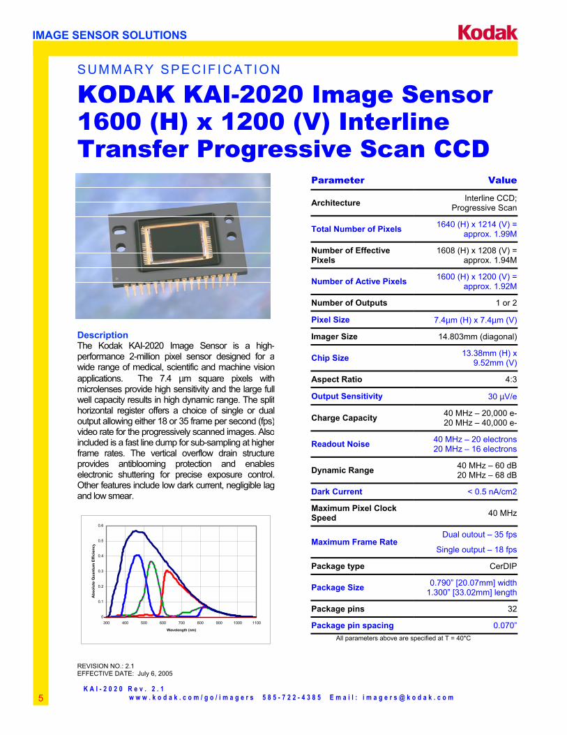
SUMMARY SPECIF ICATION
KODAK KAI-2020 Image Sensor 1600 (H) x 1200 (V) Interline Transfer Progressive Scan CCD
Description The Kodak KAI-2020 Image Sensor is a high-performance 2-million pixel sensor designed for awide range of medical, scientific and machine visionapplications. The 7.4 µm square pixels withmicrolenses provide high sensitivity and the large fullwell capacity results in high dynamic range. The splithorizontal register offers a choice of single or dualoutput allowing either 18 or 35 frame per second (fps)video rate for the progressively scanned images. Alsoincluded is a fast line dump for sub-sampling at higherframe rates. The vertical overflow drain structureprovides antiblooming protection and enableselectronic shuttering for precise exposure control.Other features include low dark current, negligible lagand low smear.
0
0.1
0.2
0.3
0.4
0.5
0.6
300 400 500 600 700 800 900 1000 1100
Wavelength (nm)
Abs
olut
e Q
uant
um E
ffici
ency
REVISION NO.: 2.1 EFFECTIVE DATE: July 6, 2005
Parameter Value
Architecture Interline CCD; Progressive Scan
Total Number of Pixels 1640 (H) x 1214 (V) = approx. 1.99M
Number of Effective Pixels
1608 (H) x 1208 (V) = approx. 1.94M
Number of Active Pixels 1600 (H) x 1200 (V) = approx. 1.92M
Number of Outputs 1 or 2
Pixel Size 7.4µm (H) x 7.4µm (V)
Imager Size 14.803mm (diagonal)
Chip Size 13.38mm (H) x 9.52mm (V)
Aspect Ratio 4:3
Output Sensitivity 30 µV/e
Charge Capacity 40 MHz – 20,000 e-20 MHz – 40,000 e-
Readout Noise 40 MHz – 20 electrons 20 MHz – 16 electrons
Dynamic Range 40 MHz – 60 dB 20 MHz – 68 dB
Dark Current < 0.5 nA/cm2
Maximum Pixel Clock Speed 40 MHz
Maximum Frame Rate Dual outout – 35 fps
Single output – 18 fps
Package type CerDIP
Package Size 0.790” [20.07mm] width 1.300” [33.02mm] length
Package pins 32
Package pin spacing 0.070”All parameters above are specified at T = 40*C
K A I - 2 0 2 0 R e v . 2 . 1 w w w . k o d a k . c o m / g o / i m a g e r s 5 8 5 - 7 2 2 - 4 3 8 5 E m a i l : i m a g e r s @ k o d a k . c o m
IMAGE SENSOR SOLUTIONS
6
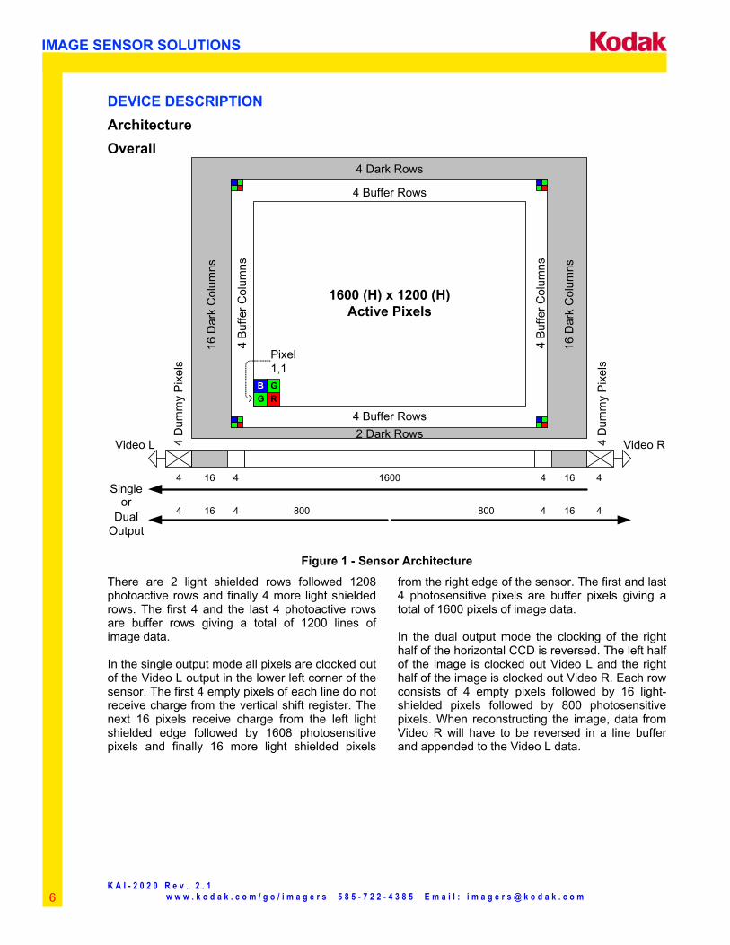
DEVICE DESCRIPTION Architecture Overall
4B
uffe
r Row
s
1600 (H) x 1200 (H)Active Pixels
4 Buffer Rows2 Dark Rows
4 Buffer Rows
4 B
uffe
r Col
umns
16 D
ark
Col
umns
16 D
ark
Col
umns
4 D
umm
y Pi
xels
4 D
umm
y Pi
xels
4 B
uffe
r Col
umns
DualOutput
or
Video L Video R
4 16 4 1600 4 16 4Single
4 16 4 800 800 4 16 4
4 Dark Rows
GGR
B
Pixel1,1
Figure 1 - Sensor Architecture
There are 2 light shielded rows followed 1208 photoactive rows and finally 4 more light shielded rows. The first 4 and the last 4 photoactive rows are buffer rows giving a total of 1200 lines of image data. In the single output mode all pixels are clocked out of the Video L output in the lower left corner of the sensor. The first 4 empty pixels of each line do not receive charge from the vertical shift register. The next 16 pixels receive charge from the left light shielded edge followed by 1608 photosensitive pixels and finally 16 more light shielded pixels
from the right edge of the sensor. The first and last 4 photosensitive pixels are buffer pixels giving a total of 1600 pixels of image data. In the dual output mode the clocking of the right half of the horizontal CCD is reversed. The left half of the image is clocked out Video L and the right half of the image is clocked out Video R. Each row consists of 4 empty pixels followed by 16 light- shielded pixels followed by 800 photosensitive pixels. When reconstructing the image, data from Video R will have to be reversed in a line buffer and appended to the Video L data.
K A I - 2 0 2 0 R e v . 2 . 1 w w w . k o d a k . c o m / g o / i m a g e r s 5 8 5 - 7 2 2 - 4 3 8 5 E m a i l : i m a g e r s @ k o d a k . c o m
IMAGE SENSOR SOLUTIONS
7
Pixel Top View
Directionof
ChargeTransfer
True Two Phase Burried Channel VCCDLightshield over VCCD not shown
7.4µm
V1Photodiode
7.4µm
V2TransferGate
Direction ofChargeTransfer
V1 V2 V1
n-n
n- n-
p Well (GND)
Cross Section Down Through VCCD
n Substrate
p
V1
np+
Light Shield
p
p
n
nSubstrate
p
Cross Section ThroughPhotodiode and VCCD Phase 1
Photodiode
p p
V2
np+
Light Shield
p
p
n
nSubstrate
p
Cross Section Through Photodiodeand VCCD Phase 2 at Transfer Gate
TransferGate
Cross Section Showing Lenslet
Lenslet
VCCD VCCDLight Shield Light Shield
Photodiode
Drawings not scale
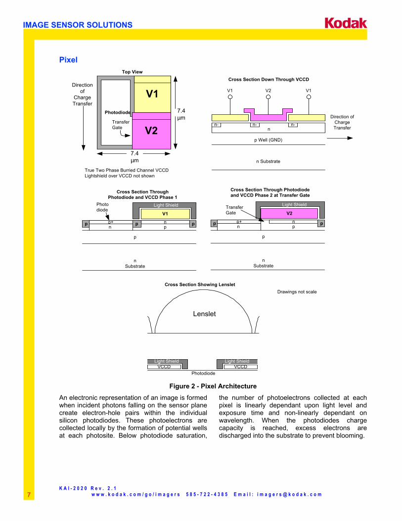
Figure 2 - Pixel Architecture
An electronic representation of an image is formed when incident photons falling on the sensor plane create electron-hole pairs within the individual silicon photodiodes. These photoelectrons are collected locally by the formation of potential wells at each photosite. Below photodiode saturation,
the number of photoelectrons collected at each pixel is linearly dependant upon light level and exposure time and non-linearly dependant on wavelength. When the photodiodes charge capacity is reached, excess electrons are discharged into the substrate to prevent blooming.
K A I - 2 0 2 0 R e v . 2 . 1 w w w . k o d a k . c o m / g o / i m a g e r s 5 8 5 - 7 2 2 - 4 3 8 5 E m a i l : i m a g e r s @ k o d a k . c o m
IMAGE SENSOR SOLUTIONS
8
Vertical to Horizontal Transfer
Top ViewDirection of
VerticalChargeTransfer
V1
V2
V1
Photodiode
V2TransferGate
FastLine
Dump
H1SH2S
H1B
H2B
Direction ofHorizontal
Charge Transfer
Lightshieldnot shown
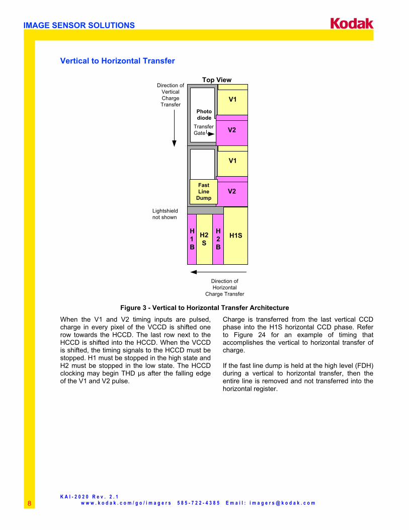
Figure 3 - Vertical to Horizontal Transfer Architecture
When the V1 and V2 timing inputs are pulsed, charge in every pixel of the VCCD is shifted one row towards the HCCD. The last row next to the HCCD is shifted into the HCCD. When the VCCD is shifted, the timing signals to the HCCD must be stopped. H1 must be stopped in the high state and H2 must be stopped in the low state. The HCCD clocking may begin THD µs after the falling edge of the V1 and V2 pulse.
Charge is transferred from the last vertical CCD phase into the H1S horizontal CCD phase. Refer to Figure 24 for an example of timing that accomplishes the vertical to horizontal transfer of charge. If the fast line dump is held at the high level (FDH) during a vertical to horizontal transfer, then the entire line is removed and not transferred into the horizontal register.
K A I - 2 0 2 0 R e v . 2 . 1 w w w . k o d a k . c o m / g o / i m a g e r s 5 8 5 - 7 2 2 - 4 3 8 5 E m a i l : i m a g e r s @ k o d a k . c o m
IMAGE SENSOR SOLUTIONS
9
Horizontal Register to Floating Diffusion
n+
R OG H2B H1B H2S H2B H1S H1B
n- n- n-
RD
FloatingDiffusion
n (burried channel)nn+
p (GND)
n (SUB)
H1S
n-
Figure 4 - Horizontal Register to Floating Diffusion Architecture
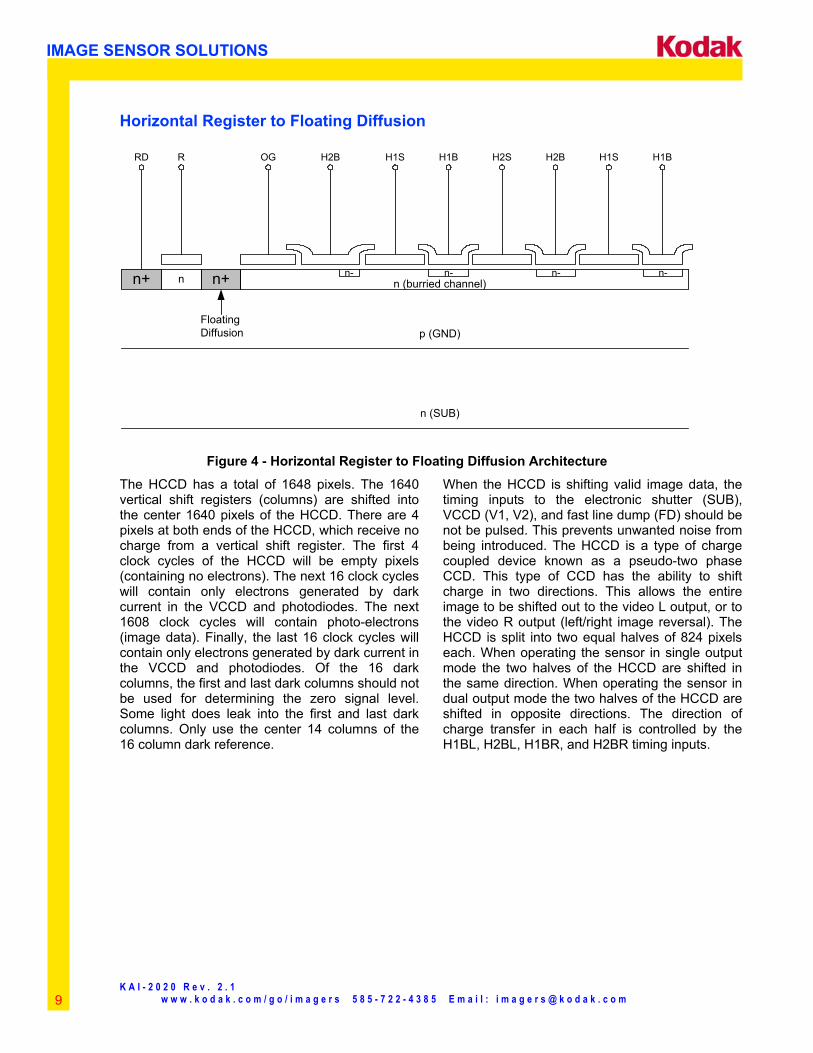
The HCCD has a total of 1648 pixels. The 1640 vertical shift registers (columns) are shifted into the center 1640 pixels of the HCCD. There are 4 pixels at both ends of the HCCD, which receive no charge from a vertical shift register. The first 4 clock cycles of the HCCD will be empty pixels (containing no electrons). The next 16 clock cycles will contain only electrons generated by dark current in the VCCD and photodiodes. The next 1608 clock cycles will contain photo-electrons (image data). Finally, the last 16 clock cycles will contain only electrons generated by dark current in the VCCD and photodiodes. Of the 16 dark columns, the first and last dark columns should not be used for determining the zero signal level. Some light does leak into the first and last dark columns. Only use the center 14 columns of the 16 column dark reference.
When the HCCD is shifting valid image data, the timing inputs to the electronic shutter (SUB), VCCD (V1, V2), and fast line dump (FD) should be not be pulsed. This prevents unwanted noise from being introduced. The HCCD is a type of charge coupled device known as a pseudo-two phase CCD. This type of CCD has the ability to shift charge in two directions. This allows the entire image to be shifted out to the video L output, or to the video R output (left/right image reversal). The HCCD is split into two equal halves of 824 pixels each. When operating the sensor in single output mode the two halves of the HCCD are shifted in the same direction. When operating the sensor in dual output mode the two halves of the HCCD are shifted in opposite directions. The direction of charge transfer in each half is controlled by the H1BL, H2BL, H1BR, and H2BR timing inputs.
K A I - 2 0 2 0 R e v . 2 . 1 w w w . k o d a k . c o m / g o / i m a g e r s 5 8 5 - 7 2 2 - 4 3 8 5 E m a i l : i m a g e r s @ k o d a k . c o m
IMAGE SENSOR SOLUTIONS
10
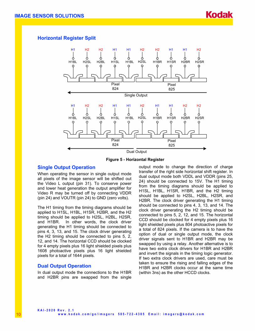
Horizontal Register Split
Single Output
H2SLH1SL H1BL H2SRH1SR H2BRH1BR
Pixel824
Pixel825
H2SL H2BLH1BL
H1 H1 H1 H1 H1H2 H2 H2 H2 H2
H2SLH1SL H1BL H2SRH1SR H2BRH1BR
Pixel824
Pixel825
H2SL H2BLH1BL
H1 H1 H1 H1 H2H2 H2 H2 H1 H2
Dual Output
Figure 5 - Horizontal Register
Single Output Operation When operating the sensor in single output mode all pixels of the image sensor will be shifted out the Video L output (pin 31). To conserve power and lower heat generation the output amplifier for Video R may be turned off by connecting VDDR (pin 24) and VOUTR (pin 24) to GND (zero volts). The H1 timing from the timing diagrams should be applied to H1SL, H1BL, H1SR, H2BR, and the H2 timing should be applied to H2SL, H2BL, H2SR, and H1BR. In other words, the clock driver generating the H1 timing should be connected to pins 4, 3, 13, and 15. The clock driver generating the H2 timing should be connected to pins 5, 2, 12, and 14. The horizontal CCD should be clocked for 4 empty pixels plus 16 light shielded pixels plus 1608 photoactive pixels plus 16 light shielded pixels for a total of 1644 pixels.
Dual Output Operation In dual output mode the connections to the H1BR and H2BR pins are swapped from the single
output mode to change the direction of charge transfer of the right side horizontal shift register. In dual output mode both VDDL and VDDR (pins 25, 24) should be connected to 15V. The H1 timing from the timing diagrams should be applied to H1SL, H1BL, H1SR, H1BR, and the H2 timing should be applied to H2SL, H2BL, H2SR, and H2BR. The clock driver generating the H1 timing should be connected to pins 4, 3, 13, and 14. The clock driver generating the H2 timing should be connected to pins 5, 2, 12, and 15. The horizontal CCD should be clocked for 4 empty pixels plus 16 light shielded pixels plus 804 photoactive pixels for a total of 824 pixels. If the camera is to have the option of dual or single output mode, the clock driver signals sent to H1BR and H2BR may be swapped by using a relay. Another alternative is to have two extra clock drivers for H1BR and H2BR and invert the signals in the timing logic generator. If two extra clock drivers are used, care must be taken to ensure the rising and falling edges of the H1BR and H2BR clocks occur at the same time (within 3ns) as the other HCCD clocks.
K A I - 2 0 2 0 R e v . 2 . 1 w w w . k o d a k . c o m / g o / i m a g e r s 5 8 5 - 7 2 2 - 4 3 8 5 E m a i l : i m a g e r s @ k o d a k . c o m
IMAGE SENSOR SOLUTIONS
11
Output
FloatingDiffusion
HCCDChargeTransfer
SourceFollower#1
SourceFollower#2
SourceFollower#3
RD
R
OG
H2B
H1B
H2S
H2B
H1S
VDD
VOUT
H1S
VDD
VSS
Figure 6 - Output Architecture
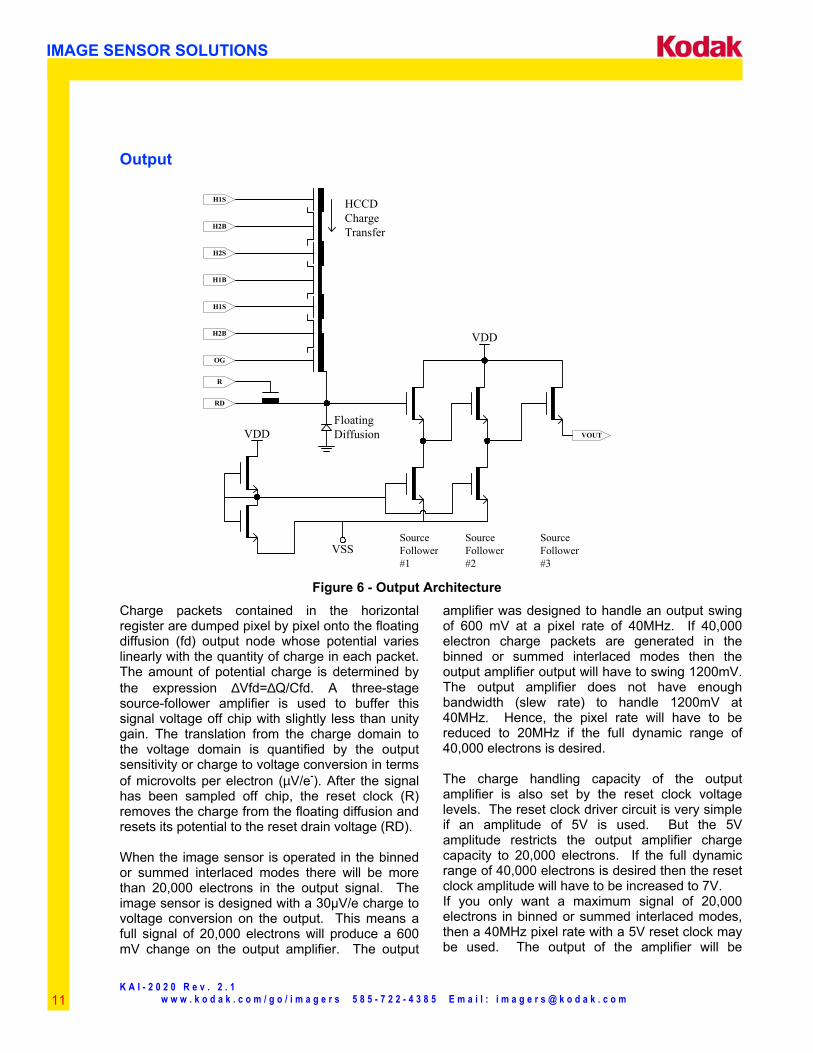
Charge packets contained in the horizontal register are dumped pixel by pixel onto the floating diffusion (fd) output node whose potential varies linearly with the quantity of charge in each packet. The amount of potential charge is determined by the expression ∆Vfd=∆Q/Cfd. A three-stage source-follower amplifier is used to buffer this signal voltage off chip with slightly less than unity gain. The translation from the charge domain to the voltage domain is quantified by the output sensitivity or charge to voltage conversion in terms of microvolts per electron (µV/e-). After the signal has been sampled off chip, the reset clock (R) removes the charge from the floating diffusion and resets its potential to the reset drain voltage (RD). When the image sensor is operated in the binned or summed interlaced modes there will be more than 20,000 electrons in the output signal. The image sensor is designed with a 30µV/e charge to voltage conversion on the output. This means a full signal of 20,000 electrons will produce a 600 mV change on the output amplifier. The output
amplifier was designed to handle an output swing of 600 mV at a pixel rate of 40MHz. If 40,000 electron charge packets are generated in the binned or summed interlaced modes then the output amplifier output will have to swing 1200mV. The output amplifier does not have enough bandwidth (slew rate) to handle 1200mV at 40MHz. Hence, the pixel rate will have to be reduced to 20MHz if the full dynamic range of 40,000 electrons is desired. The charge handling capacity of the output amplifier is also set by the reset clock voltage levels. The reset clock driver circuit is very simple if an amplitude of 5V is used. But the 5V amplitude restricts the output amplifier charge capacity to 20,000 electrons. If the full dynamic range of 40,000 electrons is desired then the reset clock amplitude will have to be increased to 7V. If you only want a maximum signal of 20,000 electrons in binned or summed interlaced modes, then a 40MHz pixel rate with a 5V reset clock may be used. The output of the amplifier will be
K A I - 2 0 2 0 R e v . 2 . 1 w w w . k o d a k . c o m / g o / i m a g e r s 5 8 5 - 7 2 2 - 4 3 8 5 E m a i l : i m a g e r s @ k o d a k . c o m
IMAGE SENSOR SOLUTIONS
12
unpredictable above 20,000 electrons so be sure to set the maximum input signal level of your
analog to digital converter to the equivalent of 20,000 electrons (600mV).
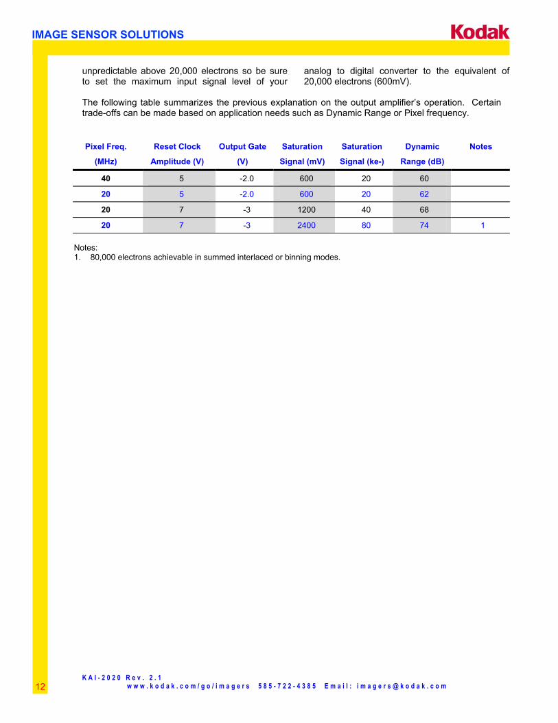
The following table summarizes the previous explanation on the output amplifier’s operation. Certain trade-offs can be made based on application needs such as Dynamic Range or Pixel frequency. Pixel Freq.
(MHz)
Reset Clock
Amplitude (V)
Output Gate
(V)
Saturation
Signal (mV)
Saturation
Signal (ke-)
Dynamic
Range (dB)
Notes
40 5 -2.0 600 20 60
20 5 -2.0 600 20 62
20 7 -3 1200 40 68
20 7 -3 2400 80 74 1 Notes: 1. 80,000 electrons achievable in summed interlaced or binning modes.
K A I - 2 0 2 0 R e v . 2 . 1 w w w . k o d a k . c o m / g o / i m a g e r s 5 8 5 - 7 2 2 - 4 3 8 5 E m a i l : i m a g e r s @ k o d a k . c o m
IMAGE SENSOR SOLUTIONS
13
ESD Protection
RL H1SL H2SL H1BL H2BL OGR/OGL
RR H1SR H2SR H1BR H2BR
ESD
VSUBD1
D2 D2 D2 D2 D2
D2D2D2D2D2D2
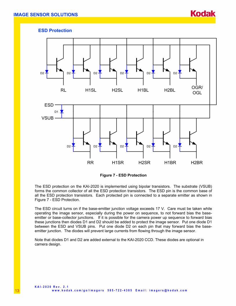
Figure 7 - ESD Protection
The ESD protection on the KAI-2020 is implemented using bipolar transistors. The substrate (VSUB) forms the common collector of all the ESD protection transistors. The ESD pin is the common base of all the ESD protection transistors. Each protected pin is connected to a separate emitter as shown in Figure 7 - ESD Protection. The ESD circuit turns on if the base-emitter junction voltage exceeds 17 V. Care must be taken while operating the image sensor, especially during the power on sequence, to not forward bias the base-emitter or base-collector junctions. If it is possible for the camera power up sequence to forward bias these junctions then diodes D1 and D2 should be added to protect the image sensor. Put one diode D1 between the ESD and VSUB pins. Put one diode D2 on each pin that may forward bias the base-emitter junction. The diodes will prevent large currents from flowing through the image sensor. Note that diodes D1 and D2 are added external to the KAI-2020 CCD. These diodes are optional in camera design.
K A I - 2 0 2 0 R e v . 2 . 1 w w w . k o d a k . c o m / g o / i m a g e r s 5 8 5 - 7 2 2 - 4 3 8 5 E m a i l : i m a g e r s @ k o d a k . c o m
IMAGE SENSOR SOLUTIONS
14
Physical Description
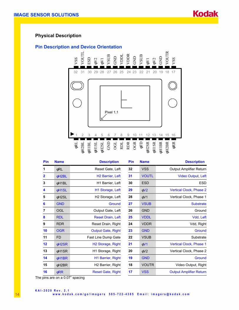
Pin Description and Device Orientation
VSS
VO
UTL
ESD
φV2
φV1
VSU
B
GN
D
VD
DL
VD
DR
GN
D
VSU
B
φV1
φV2
GN
D
VO
UTR
VSS
φRR
φRL
φH2B
L
φH1B
L
φH1S
L
φH2S
L
OG
L
OG
R
RD
R
RD
L
φH2S
R
φH1S
R
φH1B
R
φH2B
R
GN
D
φFD
Pixel 1,1
1732
1 16
31 30 29 28 27 26 25 24 23 22 21 20 19 18
2 3 4 5 6 7 8 9 151413121110
Pin Name Description Pin Name Description
1 φRL Reset Gate, Left 32 VSS Output Amplifier Return
2 φH2BL H2 Barrier, Left 31 VOUTL Video Output, Left
3 φH1BL H1 Barrier, Left 30 ESD ESD
4 φH1SL H1 Storage, Left 29 φV2 Vertical Clock, Phase 2
5 φH2SL H2 Storage, Left 28 φV1 Vertical Clock, Phase 1
6 GND Ground 27 VSUB Substrate
7 OGL Output Gate, Left 26 GND Ground
8 RDL Reset Drain, Left 25 VDDL Vdd, Left
9 RDR Reset Drain, Right 24 VDDR Vdd, Right
10 OGR Output Gate, Right 23 GND Ground
11 FD Fast Line Dump Gate 22 VSUB Substrate
12 φH2SR H2 Storage, Right 21 φV1 Vertical Clock, Phase 1
13 φH1SR H1 Storage, Right 20 φV2 Vertical Clock, Phase 2
14 φH1BR H1 Barrier, Right 19 GND Ground
15 φH2BR H2 Barrier, Right 18 VOUTR Video Output, Right
16 φRR Reset Gate, Right 17 VSS Output Amplifier ReturnThe pins are on a 0.07” spacing
K A I - 2 0 2 0 R e v . 2 . 1 w w w . k o d a k . c o m / g o / i m a g e r s 5 8 5 - 7 2 2 - 4 3 8 5 E m a i l : i m a g e r s @ k o d a k . c o m
IMAGE SENSOR SOLUTIONS
15
PERFORMANCE
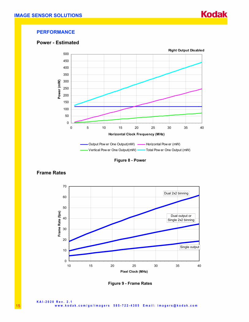
Power - Estimated
0
50
100
150
200
250
300
350
400
450
500
0 5 10 15 20 25 30 35 40
Horizontal Clock Frequency (MHz)
Pow
er (m
W)
Output Pow er One Output(mW) Horizontal Pow er (mW)
Vertical Pow er One Output(mW) Total Pow er One Output (mW)
Right Output Disabled
Figure 8 - Power
Frame Rates
0
10
20
30
40
50
60
70
10 15 20 25 30 35 40
Pixel Clock (MHz)
Fram
e R
ate
(fps)
Single output
Dual output orSingle 2x2 binning
Dual 2x2 binning
Figure 9 - Frame Rates
K A I - 2 0 2 0 R e v . 2 . 1 w w w . k o d a k . c o m / g o / i m a g e r s 5 8 5 - 7 2 2 - 4 3 8 5 E m a i l : i m a g e r s @ k o d a k . c o m
IMAGE SENSOR SOLUTIONS
16
Imaging Performance
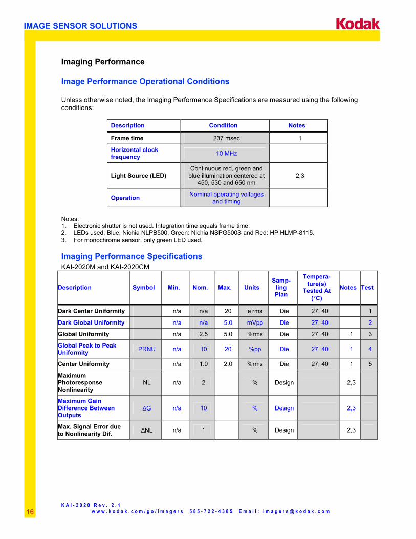
Image Performance Operational Conditions Unless otherwise noted, the Imaging Performance Specifications are measured using the following conditions:
Description Condition Notes
Frame time 237 msec 1
Horizontal clock frequency 10 MHz
Light Source (LED) Continuous red, green and
blue illumination centered at 450, 530 and 650 nm
2,3
Operation Nominal operating voltages and timing
Notes: 1. Electronic shutter is not used. Integration time equals frame time. 2. LEDs used: Blue: Nichia NLPB500, Green: Nichia NSPG500S and Red: HP HLMP-8115. 3. For monochrome sensor, only green LED used.
Imaging Performance Specifications KAI-2020M and KAI-2020CM
Description Symbol Min. Nom. Max. Units Samp-
ling Plan
Tempera-ture(s)
Tested At (°C)
Notes Test
Dark Center Uniformity n/a n/a 20 e-rms Die 27, 40 1
Dark Global Uniformity n/a n/a 5.0 mVpp Die 27, 40 2
Global Uniformity n/a 2.5 5.0 %rms Die 27, 40 1 3
Global Peak to Peak Uniformity PRNU n/a 10 20 %pp Die 27, 40 1 4
Center Uniformity n/a 1.0 2.0 %rms Die 27, 40 1 5
Maximum Photoresponse Nonlinearity
NL n/a 2 % Design 2,3
Maximum Gain Difference Between Outputs
∆G n/a 10 % Design 2,3
Max. Signal Error due to Nonlinearity Dif. ∆NL n/a 1 % Design 2,3
K A I - 2 0 2 0 R e v . 2 . 1 w w w . k o d a k . c o m / g o / i m a g e r s 5 8 5 - 7 2 2 - 4 3 8 5 E m a i l : i m a g e r s @ k o d a k . c o m
IMAGE SENSOR SOLUTIONS
17
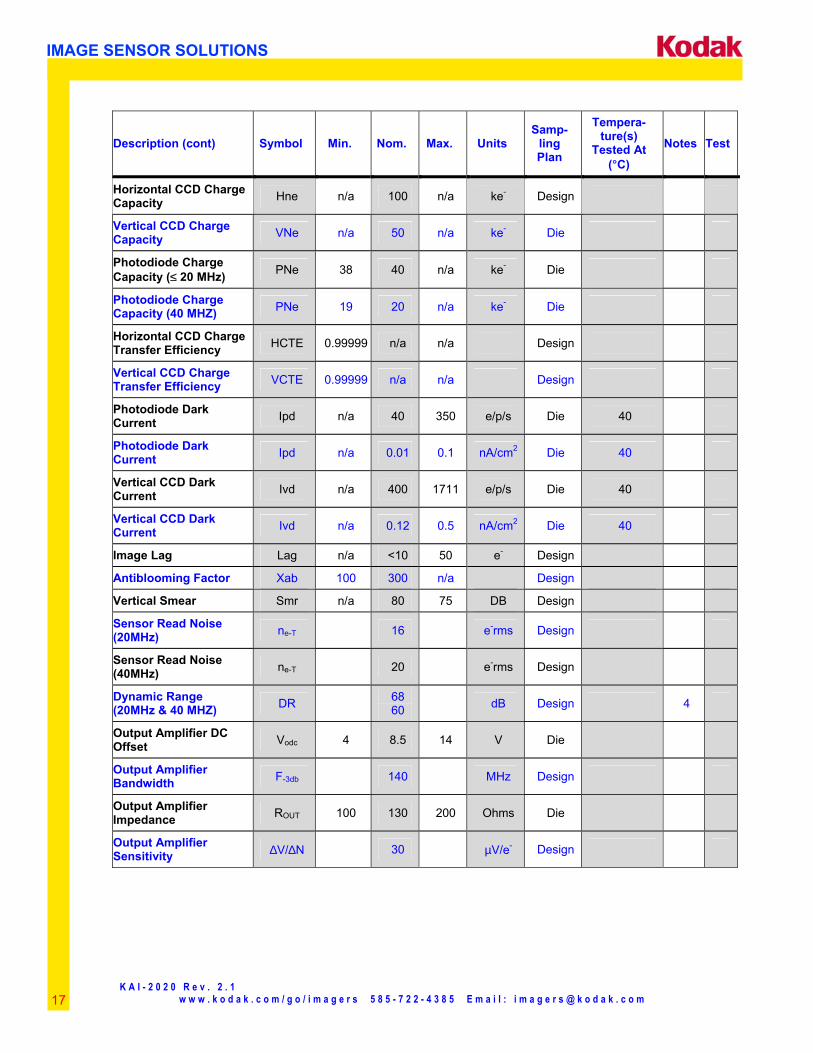
Description (cont) Symbol Min. Nom. Max. Units Samp-
ling Plan
Tempera-ture(s)
Tested At (°C)
Notes Test
Horizontal CCD Charge Capacity Hne n/a 100 n/a ke- Design
Vertical CCD Charge Capacity VNe n/a 50 n/a ke- Die
Photodiode Charge Capacity (≤ 20 MHz) PNe 38 40 n/a ke- Die
Photodiode Charge Capacity (40 MHZ) PNe 19 20 n/a ke- Die
Horizontal CCD Charge Transfer Efficiency HCTE 0.99999 n/a n/a Design
Vertical CCD Charge Transfer Efficiency VCTE 0.99999 n/a n/a Design
Photodiode Dark Current Ipd n/a 40 350 e/p/s Die 40
Photodiode Dark Current Ipd n/a 0.01 0.1 nA/cm2 Die 40
Vertical CCD Dark Current Ivd n/a 400 1711 e/p/s Die 40
Vertical CCD Dark Current Ivd n/a 0.12 0.5 nA/cm2 Die 40
Image Lag Lag n/a <10 50 e- Design
Antiblooming Factor Xab 100 300 n/a Design
Vertical Smear Smr n/a 80 75 DB Design
Sensor Read Noise (20MHz) ne-T 16 e-rms Design
Sensor Read Noise (40MHz) ne-T 20 e-rms Design
Dynamic Range (20MHz & 40 MHZ) DR 68
60 dB Design 4
Output Amplifier DC Offset Vodc 4 8.5 14 V Die
Output Amplifier Bandwidth F-3db 140 MHz Design
Output Amplifier Impedance ROUT 100 130 200 Ohms Die
Output Amplifier Sensitivity ∆V/∆N 30 µV/e- Design
K A I - 2 0 2 0 R e v . 2 . 1 w w w . k o d a k . c o m / g o / i m a g e r s 5 8 5 - 7 2 2 - 4 3 8 5 E m a i l : i m a g e r s @ k o d a k . c o m
IMAGE SENSOR SOLUTIONS
18
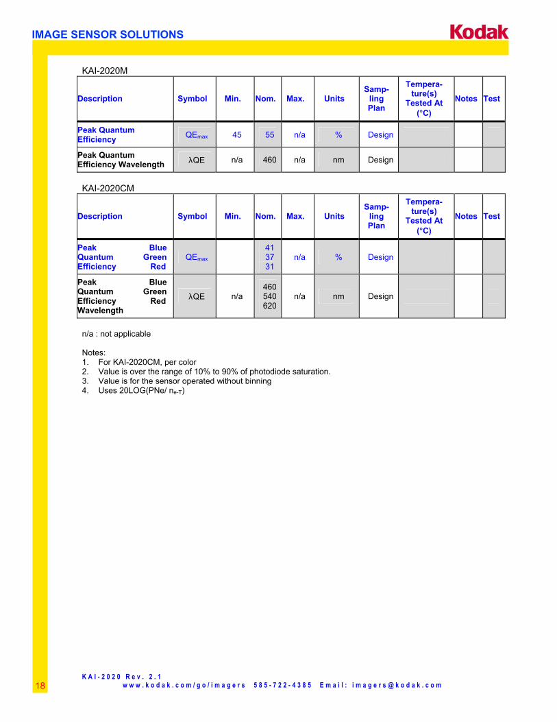
KAI-2020M
Description Symbol Min. Nom. Max. Units Samp-
ling Plan
Tempera-ture(s)
Tested At (°C)
Notes Test
Peak Quantum Efficiency QEmax 45 55 n/a % Design
Peak Quantum Efficiency Wavelength λQE n/a 460 n/a nm Design
KAI-2020CM
Description Symbol Min. Nom. Max. Units Samp-
ling Plan
Tempera-ture(s)
Tested At (°C)
Notes Test
Peak Blue Quantum Green Efficiency Red
QEmax 41 37 31
n/a % Design
Peak Blue Quantum Green Efficiency Red Wavelength
λQE n/a 460 540 620
n/a nm Design
n/a : not applicable Notes: 1. For KAI-2020CM, per color 2. Value is over the range of 10% to 90% of photodiode saturation. 3. Value is for the sensor operated without binning 4. Uses 20LOG(PNe/ ne-T)
K A I - 2 0 2 0 R e v . 2 . 1 w w w . k o d a k . c o m / g o / i m a g e r s 5 8 5 - 7 2 2 - 4 3 8 5 E m a i l : i m a g e r s @ k o d a k . c o m
IMAGE SENSOR SOLUTIONS
19
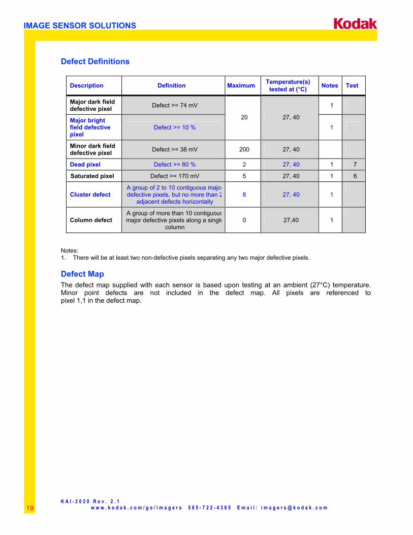
Defect Definitions
Description Definition Maximum Temperature(s) tested at (°C) Notes Test
Major dark field defective pixel Defect >= 74 mV 1
Major bright field defective pixel
Defect >= 10 % 20 27, 40
1
Minor dark field defective pixel Defect >= 38 mV 200 27, 40
Dead pixel Defect >= 80 % 2 27, 40 1 7
Saturated pixel Defect >= 170 mV 5 27, 40 1 6
Cluster defect A group of 2 to 10 contiguous major defective pixels, but no more than 2
adjacent defects horizontally 8 27, 40 1
Column defect A group of more than 10 contiguous major defective pixels along a single
column 0 27,40 1
Notes: 1. There will be at least two non-defective pixels separating any two major defective pixels.
Defect Map The defect map supplied with each sensor is based upon testing at an ambient (27°C) temperature. Minor point defects are not included in the defect map. All pixels are referenced to pixel 1,1 in the defect map.
K A I - 2 0 2 0 R e v . 2 . 1 w w w . k o d a k . c o m / g o / i m a g e r s 5 8 5 - 7 2 2 - 4 3 8 5 E m a i l : i m a g e r s @ k o d a k . c o m
IMAGE SENSOR SOLUTIONS
20
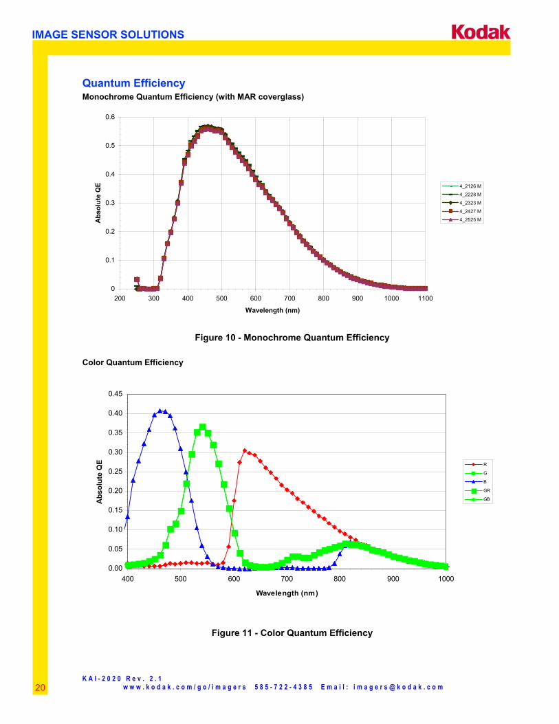
Quantum Efficiency Monochrome Quantum Efficiency (with MAR coverglass)
Figure 10 - Monochrome Quantum Efficiency Color Quantum Efficiency
Figure 11 - Color Quantum Efficiency
0
0.1
0.2
0.3
0.4
0.5
0.6
200 300 400 500 600 700 800 900 1000 1100
Wavelength (nm)
Abs
olut
e Q
E 4_2126 M
4_2228 M
4_2323 M
4_2427 M
4_2525 M
0.00
0.05
0.10
0.15
0.20
0.25
0.30
0.35
0.40
0.45
400 500 600 700 800 900 1000
Wavelength (nm)
Abs
olut
e Q
E R
G
B
GR
GB
K A I - 2 0 2 0 R e v . 2 . 1 w w w . k o d a k . c o m / g o / i m a g e r s 5 8 5 - 7 2 2 - 4 3 8 5 E m a i l : i m a g e r s @ k o d a k . c o m
IMAGE SENSOR SOLUTIONS
21
Ultraviolet (UV) Quantum Efficiency
0.0
2.0
4.0
6.0
8.0
10.0
12.0
240 340 440 540 640 740 840 940
Wavelength (nm)
AbsoluteQuantumEfficiency
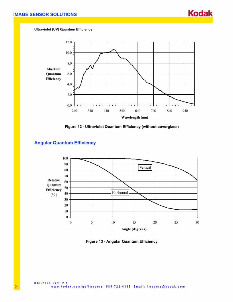
Figure 12 - Ultraviolet Quantum Efficiency (without coverglass)
Angular Quantum Efficiency
0102030405060708090
100
0 5 10 15 20 25 30
Angle (degrees)
RelativeQuantumEfficiency
(% ) Horizontal
Vertical
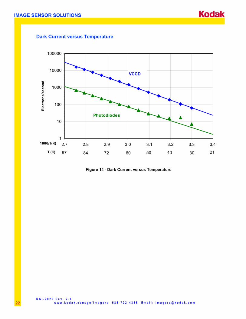
Figure 13 - Angular Quantum Efficiency
K A I - 2 0 2 0 R e v . 2 . 1 w w w . k o d a k . c o m / g o / i m a g e r s 5 8 5 - 7 2 2 - 4 3 8 5 E m a i l : i m a g e r s @ k o d a k . c o m
IMAGE SENSOR SOLUTIONS
22
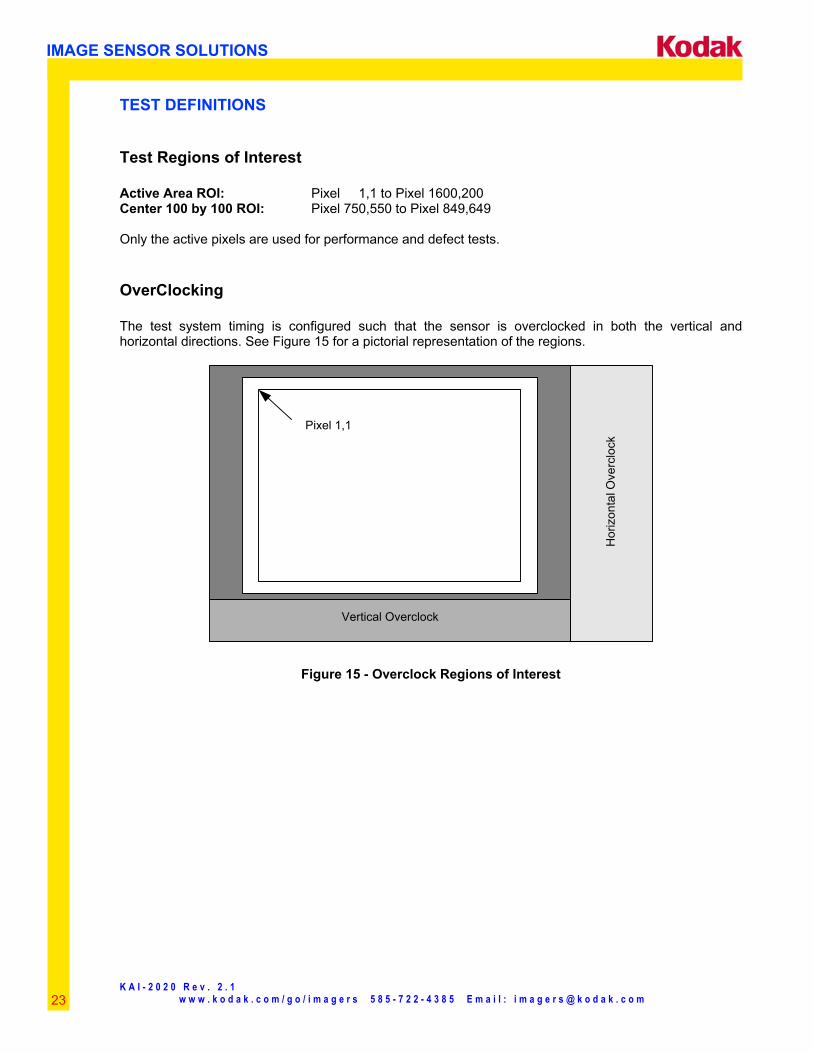
Dark Current versus Temperature
1
10
100
1000
10000
100000
2.7 2.8 2.9 3.0 3.1 3.2 3.3 3.41000/T(K)
Elec
tron
s/se
cond
T (C) 97 84 72 60 50 40 30 21
VCCD
Photodiodes
Figure 14 - Dark Current versus Temperature
K A I - 2 0 2 0 R e v . 2 . 1 w w w . k o d a k . c o m / g o / i m a g e r s 5 8 5 - 7 2 2 - 4 3 8 5 E m a i l : i m a g e r s @ k o d a k . c o m
IMAGE SENSOR SOLUTIONS
23
TEST DEFINITIONS
Test Regions of Interest Active Area ROI: Pixel 1,1 to Pixel 1600,200 Center 100 by 100 ROI: Pixel 750,550 to Pixel 849,649 Only the active pixels are used for performance and defect tests.
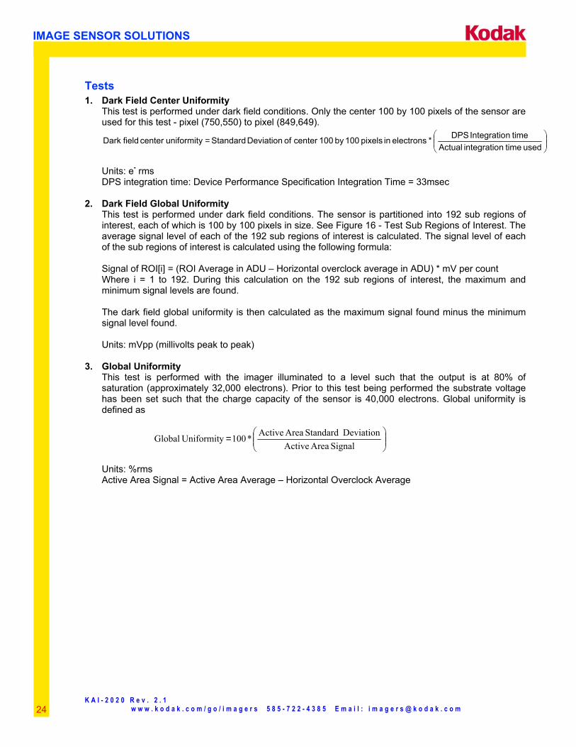
OverClocking The test system timing is configured such that the sensor is overclocked in both the vertical and horizontal directions. See Figure 15 for a pictorial representation of the regions.
Pixel 1,1
Vertical OverclockH
oriz
onta
l Ove
rclo
ck
Figure 15 - Overclock Regions of Interest
K A I - 2 0 2 0 R e v . 2 . 1 w w w . k o d a k . c o m / g o / i m a g e r s 5 8 5 - 7 2 2 - 4 3 8 5 E m a i l : i m a g e r s @ k o d a k . c o m
IMAGE SENSOR SOLUTIONS
24
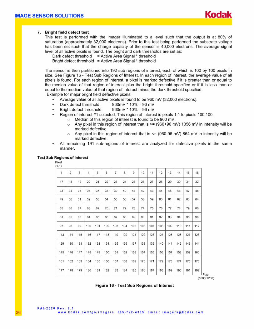
Tests 1. Dark Field Center Uniformity
This test is performed under dark field conditions. Only the center 100 by 100 pixels of the sensor are used for this test - pixel (750,550) to pixel (849,649).
=
used time nintegratio Actualtime nIntegratio DPS * electrons in pixels 100by 100 center of Deviation Standard uniformity center field Dark
Units: e- rms DPS integration time: Device Performance Specification Integration Time = 33msec
2. Dark Field Global Uniformity
This test is performed under dark field conditions. The sensor is partitioned into 192 sub regions of interest, each of which is 100 by 100 pixels in size. See Figure 16 - Test Sub Regions of Interest. The average signal level of each of the 192 sub regions of interest is calculated. The signal level of each of the sub regions of interest is calculated using the following formula: Signal of ROI[i] = (ROI Average in ADU – Horizontal overclock average in ADU) * mV per count Where i = 1 to 192. During this calculation on the 192 sub regions of interest, the maximum and minimum signal levels are found. The dark field global uniformity is then calculated as the maximum signal found minus the minimum signal level found. Units: mVpp (millivolts peak to peak)
3. Global Uniformity
This test is performed with the imager illuminated to a level such that the output is at 80% of saturation (approximately 32,000 electrons). Prior to this test being performed the substrate voltage has been set such that the charge capacity of the sensor is 40,000 electrons. Global uniformity is defined as
=
Signal Area ActiveDeviation Standard Area Active * 100 y UniformitGlobal
Units: %rms Active Area Signal = Active Area Average – Horizontal Overclock Average
K A I - 2 0 2 0 R e v . 2 . 1 w w w . k o d a k . c o m / g o / i m a g e r s 5 8 5 - 7 2 2 - 4 3 8 5 E m a i l : i m a g e r s @ k o d a k . c o m
IMAGE SENSOR SOLUTIONS
25
4. Global Peak to Peak Uniformity This test is performed with the imager illuminated to a level such that the output is at 80% of saturation (approximately 32,000 electrons). Prior to this test being performed the substrate voltage has been set such that the charge capacity of the sensor is 40,000 electrons. The sensor is partitioned into 192 sub regions of interest, each of which is 100 by 100 pixels in size. See Figure 16 - Test Sub Regions of Interest. The average signal level of each of the 192 sub regions of interest (ROI) is calculated. The signal level of each of the sub regions of interest is calculated using the following formula: Signal of ROI[i] = (ROI Average in ADU – Horizontal overclock average in ADU) * mV per count Where i = 1 to 192. During this calculation on the 192 sub regions of interest, the maximum and minimum signal levels are found. The global peak to peak uniformity is then calculated as:
Signal AreaActiveSignal Minimum - Signal Maximum Uniformity Global =
Units: %pp
5. Center Uniformity This test is performed with the imager illuminated to a level such that the output is at 80% of saturation (approximately 32,000 electrons). Prior to this test being performed the substrate voltage has been set such that the charge capacity of the sensor is 40,000 electrons. Defects are excluded for the calculation of this test. This test is performed on the center 100 by 100 pixels (See Figure 16 - Test Sub Regions of Interest) of the sensor. Center uniformity is defined as:
=
Signal ROI CenterDeviation Standard ROI Center
* 100 Uniformity ROI Center
Units: %rms Center ROI Signal = Center ROI Average – Horizontal Overclock Average
6. Dark field defect test
This test is performed under dark field conditions. The sensor is partitioned into 192 sub regions of interest, each of which is 100 by 100 pixels in size. See Figure 16 - Test Sub Regions of Interest. In each region of interest, the median value of all pixels is found. For each region of interest, a pixel is marked defective if it is greater than or equal to the median value of that region of interest plus the defect threshold specified in “Defect Definitions” section.
K A I - 2 0 2 0 R e v . 2 . 1 w w w . k o d a k . c o m / g o / i m a g e r s 5 8 5 - 7 2 2 - 4 3 8 5 E m a i l : i m a g e r s @ k o d a k . c o m
IMAGE SENSOR SOLUTIONS
26
7. Bright field defect test This test is performed with the imager illuminated to a level such that the output is at 80% of saturation (approximately 32,000 electrons). Prior to this test being performed the substrate voltage has been set such that the charge capacity of the sensor is 40,000 electrons. The average signal level of all active pixels is found. The bright and dark thresholds are set as: Dark defect threshold = Active Area Signal * threshold Bright defect threshold = Active Area Signal * threshold The sensor is then partitioned into 192 sub regions of interest, each of which is 100 by 100 pixels in size. See Figure 16 - Test Sub Regions of Interest. In each region of interest, the average value of all pixels is found. For each region of interest, a pixel is marked defective if it is greater than or equal to the median value of that region of interest plus the bright threshold specified or if it is less than or equal to the median value of that region of interest minus the dark threshold specified. Example for major bright field defective pixels:
• Average value of all active pixels is found to be 960 mV (32,000 electrons). • Dark defect threshold: 960mV * 10% = 96 mV • Bright defect threshold: 960mV * 10% = 96 mV • Region of interest #1 selected. This region of interest is pixels 1,1 to pixels 100,100.
o Median of this region of interest is found to be 960 mV. o Any pixel in this region of interest that is >= (960+96 mV) 1056 mV in intensity will be
marked defective. o Any pixel in this region of interest that is <= (960-96 mV) 864 mV in intensity will be
marked defective. • All remaining 191 sub-regions of interest are analyzed for defective pixels in the same
manner.
Test Sub Regions of Interest Pixel(1,1)
Pixel(1600,1200)
1 2 3 4 5 6 7 8 9 10
17 18 19 20 21 22 23 24 25 26
33 34 35 36 37 38 39 40 41 42
49 50 51 52 53 54 55 56 57 58
65 66 67 68 69 70 71 72 73 74
81 82 83 84 85 86 87 88 89 90
97 98 99 100 101 102 103 104 105 106
113 114 115 116 117 118 119 120 121 122
129 130 131 132 133 134 135 136 137 138
11 12 13 14 15 16
27 28 29 30 31 32
43 44 45 46 47 48
59 60 61 62 63 64
75 76 77 78 79 80
91 92 93 94 95 96
107 108 109 110 111 112
123 124 125 126 127 128
139 140 141 142 143 144
145 146 147 148 149 150 151 152 153 154 155 156 157 158 159 160
161 162 163 164 165 166 167 168 169 170 171 172 173 174 175 176
177 178 179 180 181 182 183 184 185 186 187 188 189 190 191 192
Figure 16 - Test Sub Regions of Interest
K A I - 2 0 2 0 R e v . 2 . 1 w w w . k o d a k . c o m / g o / i m a g e r s 5 8 5 - 7 2 2 - 4 3 8 5 E m a i l : i m a g e r s @ k o d a k . c o m
IMAGE SENSOR SOLUTIONS
27
OPERATION
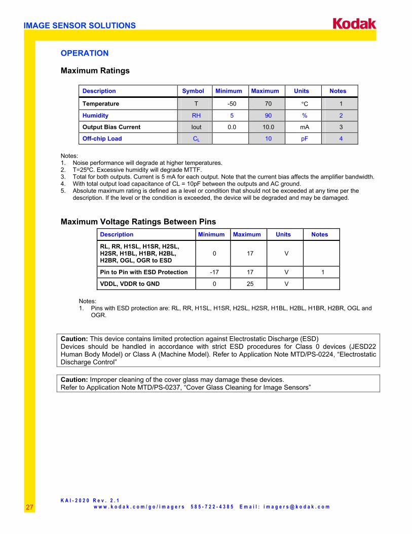
Maximum Ratings
Description Symbol Minimum Maximum Units Notes
Temperature T -50 70 °C 1
Humidity RH 5 90 % 2
Output Bias Current Iout 0.0 10.0 mA 3
Off-chip Load CL 10 pF 4 Notes: 1. Noise performance will degrade at higher temperatures. 2. T=25ºC. Excessive humidity will degrade MTTF. 3. Total for both outputs. Current is 5 mA for each output. Note that the current bias affects the amplifier bandwidth. 4. With total output load capacitance of CL = 10pF between the outputs and AC ground. 5. Absolute maximum rating is defined as a level or condition that should not be exceeded at any time per the
description. If the level or the condition is exceeded, the device will be degraded and may be damaged.
Maximum Voltage Ratings Between Pins Description Minimum Maximum Units Notes
RL, RR, H1SL, H1SR, H2SL, H2SR, H1BL, H1BR, H2BL, H2BR, OGL, OGR to ESD
0 17 V
Pin to Pin with ESD Protection -17 17 V 1
VDDL, VDDR to GND 0 25 V
Notes: 1. Pins with ESD protection are: RL, RR, H1SL, H1SR, H2SL, H2SR, H1BL, H2BL, H1BR, H2BR, OGL and
OGR.
Caution: This device contains limited protection against Electrostatic Discharge (ESD) Devices should be handled in accordance with strict ESD procedures for Class 0 devices (JESD22 Human Body Model) or Class A (Machine Model). Refer to Application Note MTD/PS-0224, “Electrostatic Discharge Control” Caution: Improper cleaning of the cover glass may damage these devices. Refer to Application Note MTD/PS-0237, “Cover Glass Cleaning for Image Sensors”
K A I - 2 0 2 0 R e v . 2 . 1 w w w . k o d a k . c o m / g o / i m a g e r s 5 8 5 - 7 2 2 - 4 3 8 5 E m a i l : i m a g e r s @ k o d a k . c o m
IMAGE SENSOR SOLUTIONS
28
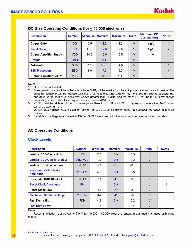
DC Bias Operating Conditions (for < 40,000 electrons)
Description Symbol Minimum Nominal Maximum Units Maximum DC Current (mA) Notes
Output Gate OG -2.5 -2.0 -1.5 V 1 µA 4
Reset Drain RD 11.5 12.0 12.5 V 1 µA 5
Output Amplifier Supply VDD 14.5 15.0 15.5 V 1 mA 1
Ground GND 0.0 V
Substrate SUB 8.0 Vab 17.0 V 2
ESD Protection ESD -8.0 -7.0 -6.0 V 3
Output Amplifier Return VSS 0.0 0.7 1.0 V Notes: 1. One output, unloaded 2. The operating value of the substrate voltage, VAB, will be marked on the shipping container for each device. The
shipping container will be marked with two VAB voltages. One VAB will be for a 600mV charge capacity (for operation of the horizontal clock frequencies greater than 20MHz) and the other VAB will be for 1200mV charge capacity (for horizontal clock frequencies at or below 20MHz).
3. VESD must be at least 1 Volt more negative than H1L, H2L and RL during sensors operation AND during camera power turn on.
4. Output gate voltage must be set to –3V for 40,000-80,000 electrons output in summed interlaced or binning modes.
5. Reset Drain voltage must be set to 13V for 80,000 electrons output in summed interlaced or binning modes.
AC Operating Conditions
Clock Levels Description Symbol Minimum Nominal Maximum Units Notes
Vertical CCD Clock High V2H 7.5 8.0 8.5 V
Vertical CCD Clocks Midlevel V1M, V2M -0.2 0.0 0.2 V
Vertical CCD Clocks Low V1L, V2L -9.5 -9.0 -8.5 V
Horizontal CCD Clocks Amplitude H1H, H2H 4.5 5.0 5.5 V
Horizontal CCD Clocks Low H1L, H2L -5.0 -4.0 -3.8 V
Reset Clock Amplitude RH 5.0 V 1
Reset Clock Low RL -4.0 -3.5 -3.0 V 2
Electronic Shutter Voltage Vshutter 44 48 52 V
Fast Dump High FDH 4.8 5.0 5.2 V
Fast Dump Low FDL -9.5 -9 -8 V Notes: 1. Reset amplitude must be set to 7.0 V for 40,000 – 80,000 electrons output in summed interlaced or binning modes.
K A I - 2 0 2 0 R e v . 2 . 1 w w w . k o d a k . c o m / g o / i m a g e r s 5 8 5 - 7 2 2 - 4 3 8 5 E m a i l : i m a g e r s @ k o d a k . c o m
IMAGE SENSOR SOLUTIONS
29
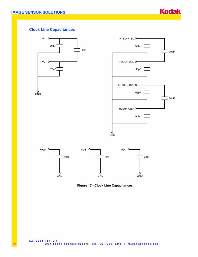
Clock Line Capacitances
V1
V2
GND
25nF
25nF
H1SL+H1BL
66pF
H2SL+H2BL
58pF
H1SR+H1BR
66pF
H2SR+H2BR
58pF
20pF
20pF
GND
GND
Reset
10pF
GND
SUB
2nF
GND
FD
21pF
5nF
Figure 17 - Clock Line Capacitances
K A I - 2 0 2 0 R e v . 2 . 1 w w w . k o d a k . c o m / g o / i m a g e r s 5 8 5 - 7 2 2 - 4 3 8 5 E m a i l : i m a g e r s @ k o d a k . c o m
IMAGE SENSOR SOLUTIONS
30
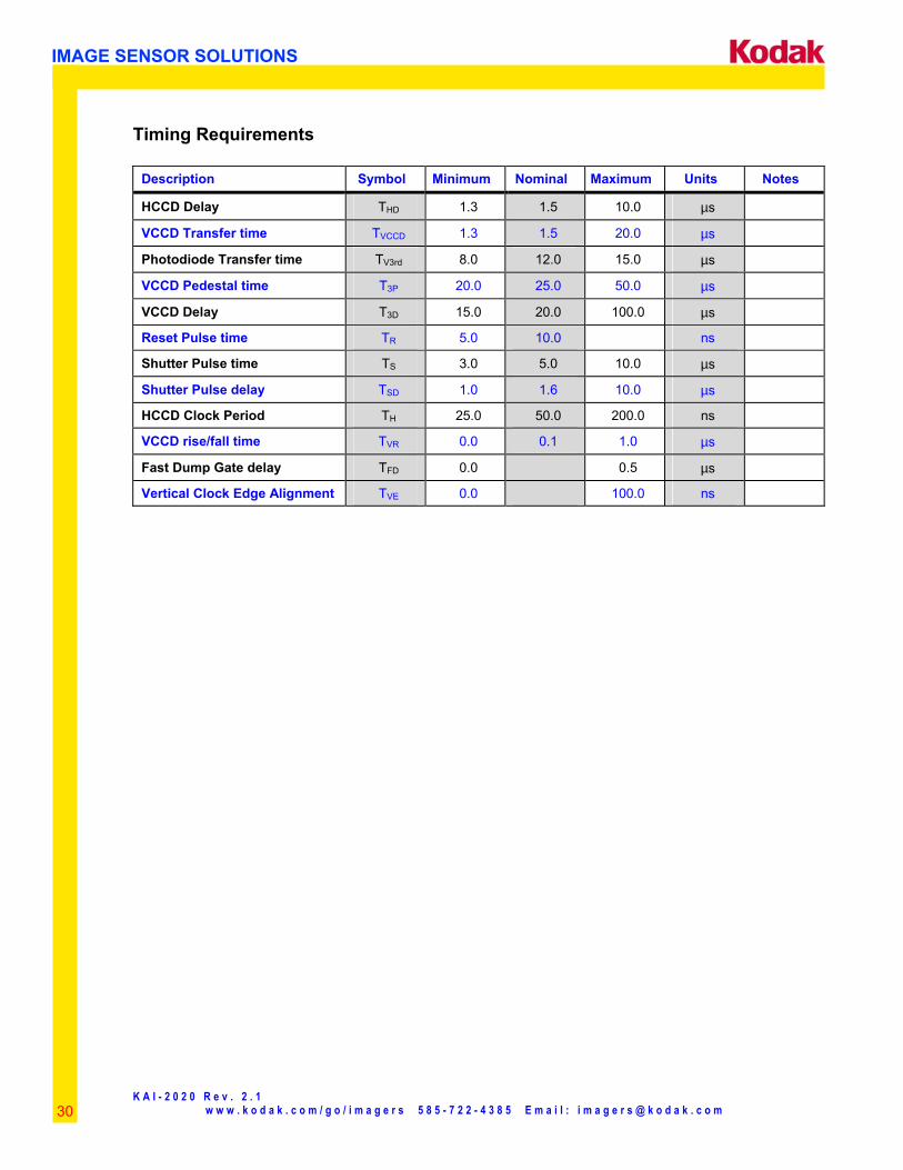
Timing Requirements
Description Symbol Minimum Nominal Maximum Units Notes
HCCD Delay THD 1.3 1.5 10.0 µs
VCCD Transfer time TVCCD 1.3 1.5 20.0 µs
Photodiode Transfer time TV3rd 8.0 12.0 15.0 µs
VCCD Pedestal time T3P 20.0 25.0 50.0 µs
VCCD Delay T3D 15.0 20.0 100.0 µs
Reset Pulse time TR 5.0 10.0 ns
Shutter Pulse time TS 3.0 5.0 10.0 µs
Shutter Pulse delay TSD 1.0 1.6 10.0 µs
HCCD Clock Period TH 25.0 50.0 200.0 ns
VCCD rise/fall time TVR 0.0 0.1 1.0 µs
Fast Dump Gate delay TFD 0.0 0.5 µs
Vertical Clock Edge Alignment TVE 0.0 100.0 ns
K A I - 2 0 2 0 R e v . 2 . 1 w w w . k o d a k . c o m / g o / i m a g e r s 5 8 5 - 7 2 2 - 4 3 8 5 E m a i l : i m a g e r s @ k o d a k . c o m
IMAGE SENSOR SOLUTIONS
31
Timing Modes
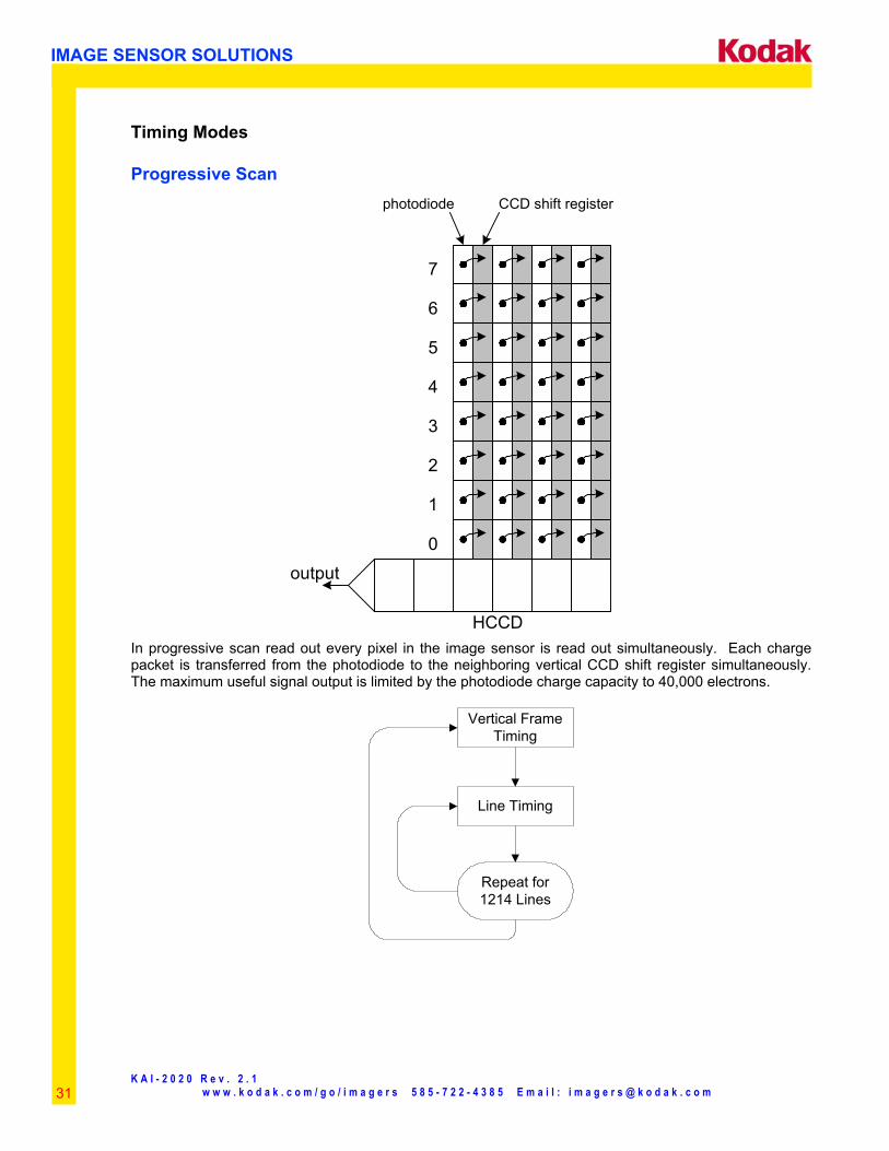
Progressive Scan photodiode CCD shift register
0
1
2
3
5
4
7
6
output
HCCD
In progressive scan read out every pixel in the image sensor is read out simultaneously. Each charge packet is transferred from the photodiode to the neighboring vertical CCD shift register simultaneously. The maximum useful signal output is limited by the photodiode charge capacity to 40,000 electrons.
Vertical FrameTiming
Line Timing
Repeat for1214 Lines
K A I - 2 0 2 0 R e v . 2 . 1 w w w . k o d a k . c o m / g o / i m a g e r s 5 8 5 - 7 2 2 - 4 3 8 5 E m a i l : i m a g e r s @ k o d a k . c o m
IMAGE SENSOR SOLUTIONS
32
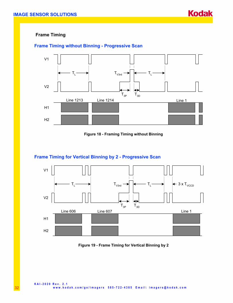
Frame Timing
Frame Timing without Binning - Progressive Scan
V1
V2
H1
H2
TL TV3rd
T3P T3D
TL
Line 1214 Line 1Line 1213
Figure 18 - Framing Timing without Binning
Frame Timing for Vertical Binning by 2 - Progressive Scan
V1
V2
H1
H2
TL TV3rd
T3P T3D
TL
Line 607 Line 1Line 606
3 x TVCCD
Figure 19 - Frame Timing for Vertical Binning by 2
K A I - 2 0 2 0 R e v . 2 . 1 w w w . k o d a k . c o m / g o / i m a g e r s 5 8 5 - 7 2 2 - 4 3 8 5 E m a i l : i m a g e r s @ k o d a k . c o m
IMAGE SENSOR SOLUTIONS
33
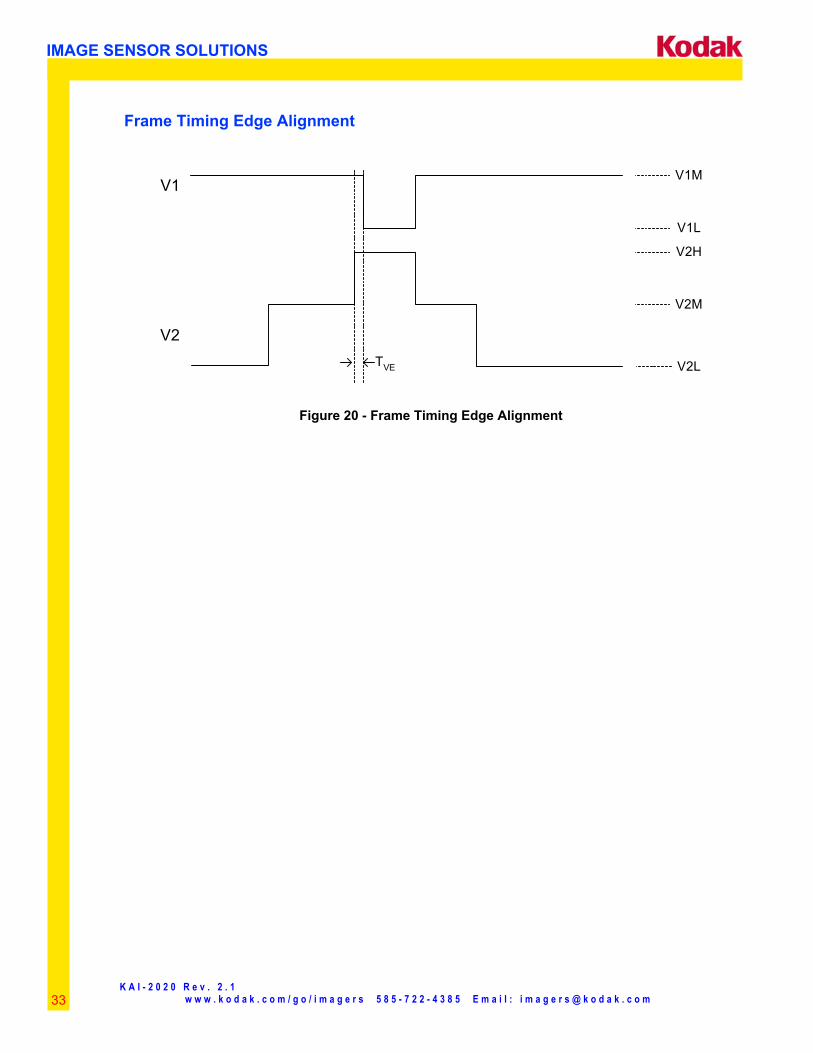
Frame Timing Edge Alignment
V1
V2TVE
V1M
V1L
V2H
V2M
V2L
Figure 20 - Frame Timing Edge Alignment
K A I - 2 0 2 0 R e v . 2 . 1 w w w . k o d a k . c o m / g o / i m a g e r s 5 8 5 - 7 2 2 - 4 3 8 5 E m a i l : i m a g e r s @ k o d a k . c o m
IMAGE SENSOR SOLUTIONS
34
Line Timing
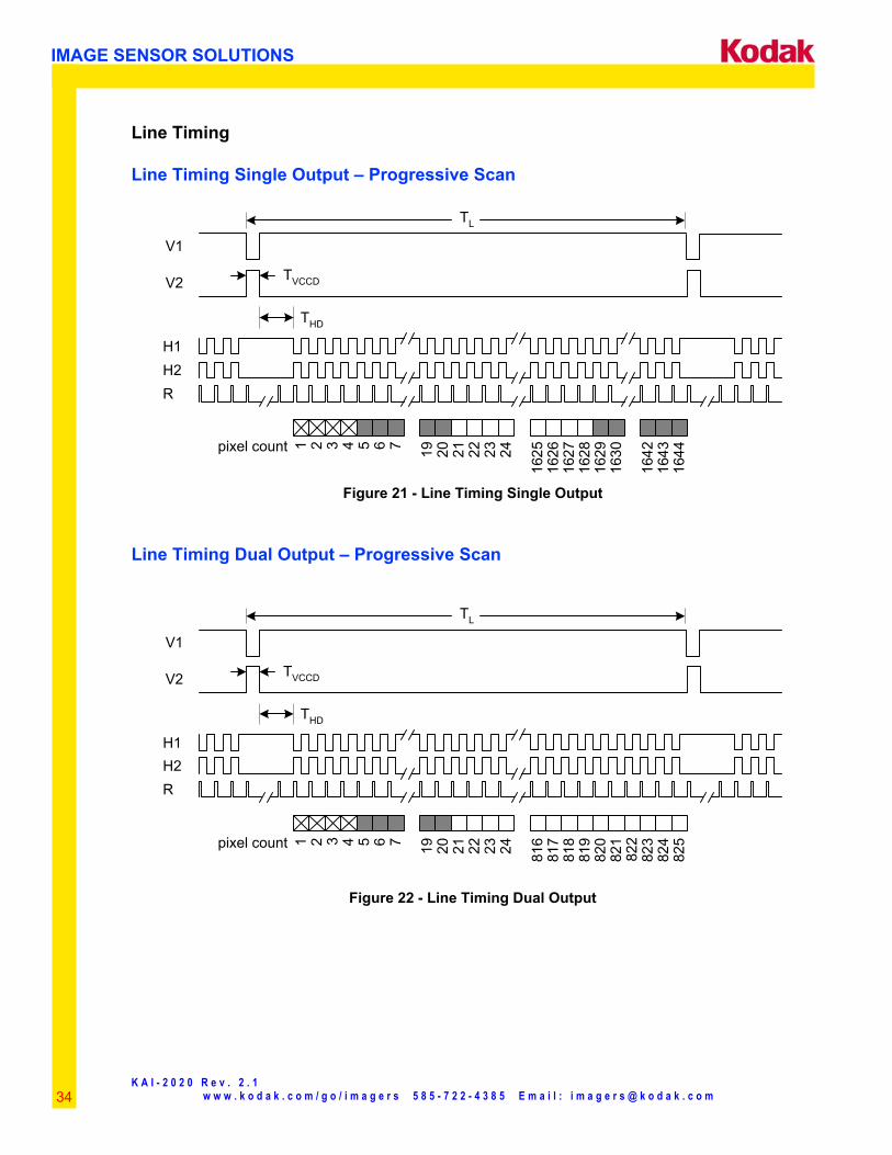
Line Timing Single Output – Progressive Scan
V1
V2 TVCCD
TL
THD
H1H2R
21pixel count 194 5 6 7 20 21 22 23
1625
1626
1627
1629
1630
1643
164424
1628
16423
Figure 21 - Line Timing Single Output
Line Timing Dual Output – Progressive Scan
V1
V2 TVCCD
TL
THD
H1H2R
21pixel count 194 5 6 7 20 21 22 23 816
817
818
820
821
824
82524 819
823
8223
Figure 22 - Line Timing Dual Output
K A I - 2 0 2 0 R e v . 2 . 1 w w w . k o d a k . c o m / g o / i m a g e r s 5 8 5 - 7 2 2 - 4 3 8 5 E m a i l : i m a g e r s @ k o d a k . c o m
IMAGE SENSOR SOLUTIONS
35
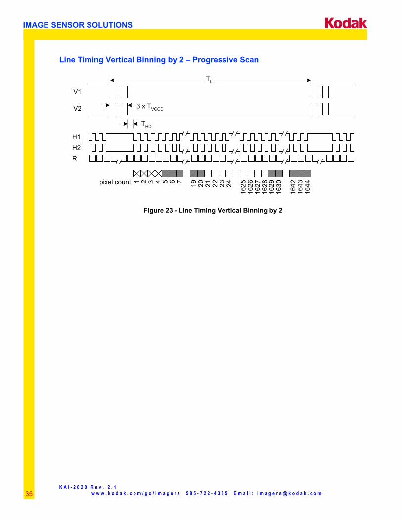
Line Timing Vertical Binning by 2 – Progressive Scan
V1
V2 3 x TVCCD
TL
THD
H1H2R
21pixel count 194 5 6 7 20 21 22 23
1625
1626
1627
1629
1630
1643
164424
1628
16423
Figure 23 - Line Timing Vertical Binning by 2
K A I - 2 0 2 0 R e v . 2 . 1 w w w . k o d a k . c o m / g o / i m a g e r s 5 8 5 - 7 2 2 - 4 3 8 5 E m a i l : i m a g e r s @ k o d a k . c o m
IMAGE SENSOR SOLUTIONS
36
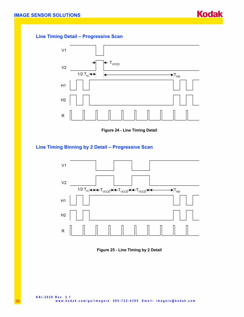
Line Timing Detail – Progressive Scan
V1
V2TVCCD
H2
THD1/2 TH
R
H1
Figure 24 - Line Timing Detail
Line Timing Binning by 2 Detail – Progressive Scan
V1
V2
TVCCD
H2
THD1/2 TH
R
H1
TVCCD TVCCD
Figure 25 - Line Timing by 2 Detail
K A I - 2 0 2 0 R e v . 2 . 1 w w w . k o d a k . c o m / g o / i m a g e r s 5 8 5 - 7 2 2 - 4 3 8 5 E m a i l : i m a g e r s @ k o d a k . c o m
IMAGE SENSOR SOLUTIONS
37
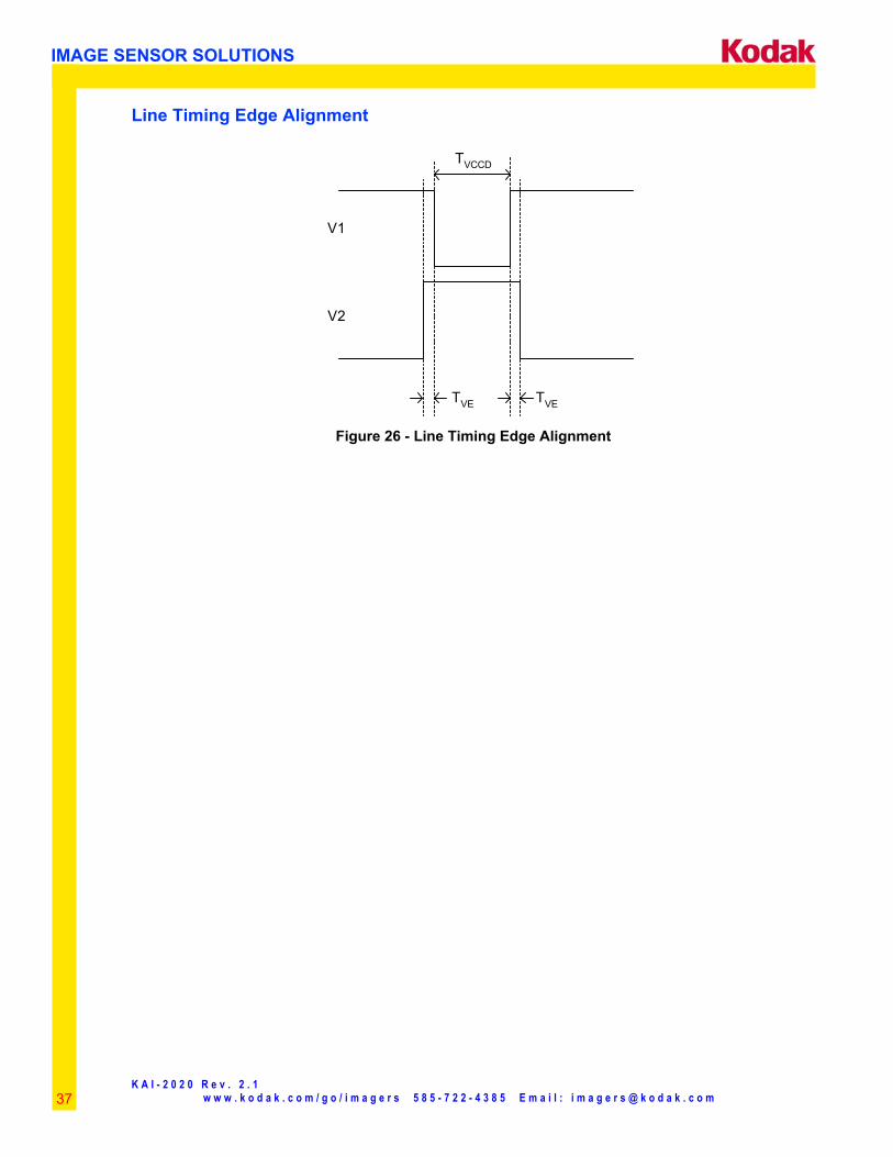
Line Timing Edge Alignment
V1
V2
TVE TVE
TVCCD
Figure 26 - Line Timing Edge Alignment
K A I - 2 0 2 0 R e v . 2 . 1 w w w . k o d a k . c o m / g o / i m a g e r s 5 8 5 - 7 2 2 - 4 3 8 5 E m a i l : i m a g e r s @ k o d a k . c o m
IMAGE SENSOR SOLUTIONS
38
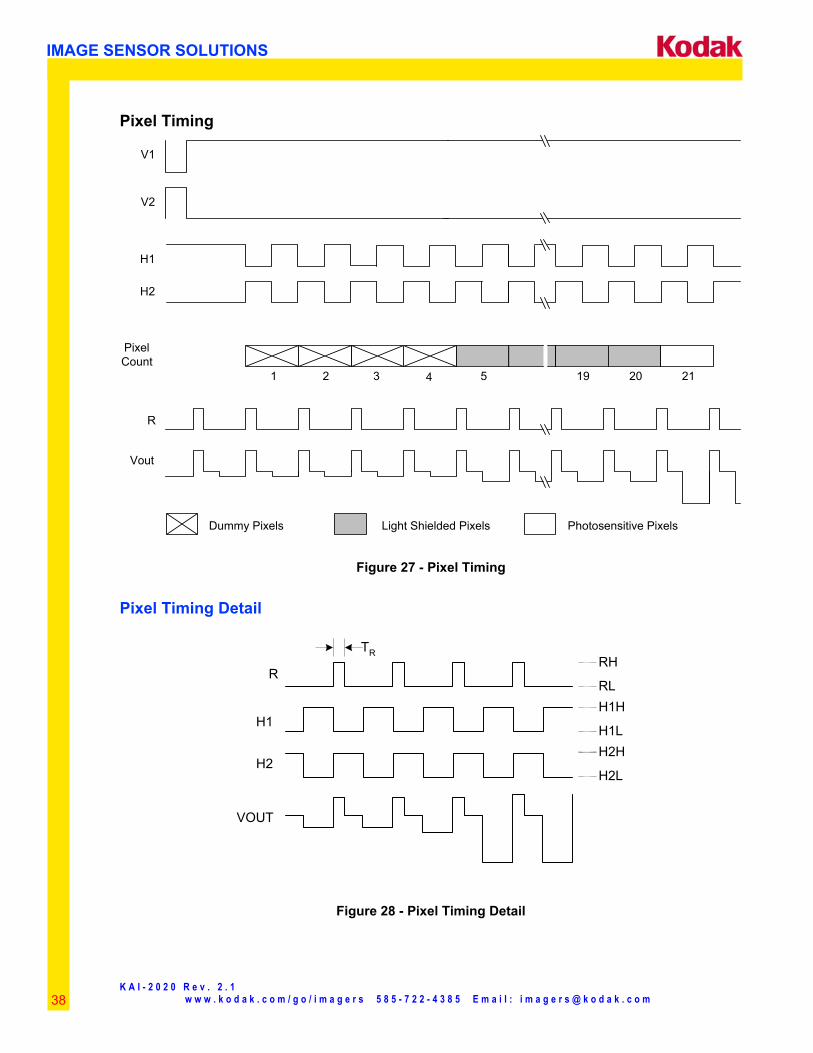
Pixel Timing
H2
R
Vout
V1
V2
PixelCount
Dummy Pixels Light Shielded Pixels Photosensitive Pixels
H1
1 5 19 20 21432
Figure 27 - Pixel Timing
Pixel Timing Detail
R
H2
VOUT
TRRH
RLH1H
H1LH2H
H2L
H1
Figure 28 - Pixel Timing Detail
K A I - 2 0 2 0 R e v . 2 . 1 w w w . k o d a k . c o m / g o / i m a g e r s 5 8 5 - 7 2 2 - 4 3 8 5 E m a i l : i m a g e r s @ k o d a k . c o m
IMAGE SENSOR SOLUTIONS
39
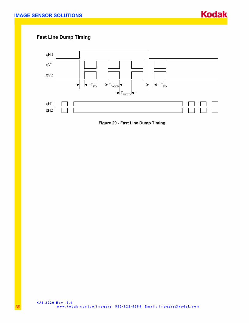
Fast Line Dump Timing
TVCCD
φV1
φV2
TFD
φFD
TFDTVCCD
φH1φH2
Figure 29 - Fast Line Dump Timing
K A I - 2 0 2 0 R e v . 2 . 1 w w w . k o d a k . c o m / g o / i m a g e r s 5 8 5 - 7 2 2 - 4 3 8 5 E m a i l : i m a g e r s @ k o d a k . c o m
IMAGE SENSOR SOLUTIONS
40
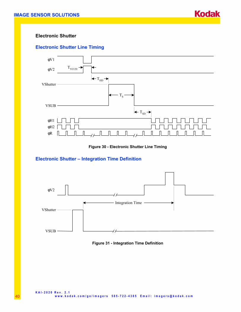
Electronic Shutter
Electronic Shutter Line Timing
φV1
φV2 TVCCD
TS
THD
φH1φH2φR
TSD
VShutter
VSUB
Figure 30 - Electronic Shutter Line Timing
Electronic Shutter – Integration Time Definition
φV2
Integration Time
VShutter
VSUB
Figure 31 - Integration Time Definition
K A I - 2 0 2 0 R e v . 2 . 1 w w w . k o d a k . c o m / g o / i m a g e r s 5 8 5 - 7 2 2 - 4 3 8 5 E m a i l : i m a g e r s @ k o d a k . c o m
IMAGE SENSOR SOLUTIONS
41
Electronic Shutter Description The voltage on the substrate (SUB) determines the charge capacity of the photodiodes. When SUB is 8 volts the photodiodes will be at their maximum charge capacity. Increasing VSUB above 8 volts decreases the charge capacity of the photodiodes until 48 volts when the photodiodes have a charge capacity of zero electrons. Therefore, a short pulse on SUB, with a peak amplitude greater than 48 volts, empties all photodiodes and provides the electronic shuttering action. It may appear the optimal substrate voltage setting is 8 volts to obtain the maximum charge capacity and dynamic range. While setting VSUB to 8 volts will provide the maximum dynamic range, it will also provide the minimum antiblooming protection. The KAI-2020 VCCD has a charge capacity of 50,000 electrons (50ke-). If the SUB voltage is set such that the photodiode holds more than 50ke-, then when the charge is transferred from a full photodiode to VCCD, the VCCD will overflow. This overflow condition manifests itself in the image by making bright spots appear elongated in the vertical direction. The size increase of a bright spot is called blooming when the spot doubles in size. The blooming can be eliminated by increasing the voltage on SUB to lower the charge capacity of the photodiode. This ensures the VCCD charge capacity is greater than the photodiode capacity. There are cases where an extremely bright spot will still cause blooming in the VCCD. Normally, when the photodiode is full, any additional electrons generated by photons will spill out of the photodiode. The excess electrons are drained harmlessly out to the substrate. There is a maximum rate at which the electrons can be drained to the substrate. If that maximum rate is exceeded, (for example, by a very bright light source) then it is possible for the total amount of charge in the photodiode to exceed the VCCD capacity. This results in blooming. The amount of antiblooming protection also decreases when the integration time is decreased. There is a compromise between photodiode dynamic range (controlled by VSUB) and the amount of antiblooming protection. A low VSUB voltage provides the maximum dynamic range and minimum (or no) antiblooming protection. A high VSUB voltage provides lower dynamic range and maximum antiblooming protection. The optimal setting of VSUB is written on the container in
which each KAI-2020 is shipped. The given VSUB voltage for each sensor is selected to provide antiblooming protection for bright spots at least 100 times saturation, while maintaining at least 40ke- of dynamic range. The electronic shutter provides a method of precisely controlling the image exposure time without any mechanical components. If an integration time of TINT is desired, then the substrate voltage of the sensor is pulsed to at least 40 volts TINT seconds before the photodiode to VCCD transfer pulse on V2. Use of the electronic shutter does not have to wait until the previously acquired image has been completely read out of the VCCD.
Large Signal Output When the image sensor is operated in the binned or summed interlaced modes there will be more than 20,000 electrons in the output signal. The image sensor is designed with a 30µV/e charge to voltage conversion on the output. This means a full signal of 40,000 electrons will produce a 600 mV change on the output amplifier. The output amplifier was designed to handle an output swing of 600mV at a pixel rate of 40MHz. If 40,000 electron charge packets are generated in the binned or summed interlaced modes then the output amplifier output will have to swing 1200 mV. The output amplifier does not have enough bandwidth (slew rate) to handle 1200 mV at 40 MHz. Hence, the pixel rate will have to be reduced to 20MHz if the full dynamic range of 40,000 electrons is desired. The charge handling capacity of the output amplifier is also set by the reset clock voltage levels. The reset clock driver circuit is very simple if an amplitude of 5V is used. But the 5V amplitude restricts the output amplifier charge capacity to 20,000 electrons. If the full dynamic range of 40,000 electrons is desired then the reset clock amplitude will have to be increased to 7V. If you only want a maximum signal of 20,000 electrons in binned or summed interlaced modes, then a 40 MHz pixel rate with a 5V reset clock may be used. The output of the amplifier will be unpredictable above 20,000 electrons so be sure to set the maximum input signal level of your analog to digital converter to the equivalent of 20,000 electrons (600mV).
K A I - 2 0 2 0 R e v . 2 . 1 w w w . k o d a k . c o m / g o / i m a g e r s 5 8 5 - 7 2 2 - 4 3 8 5 E m a i l : i m a g e r s @ k o d a k . c o m
IMAGE SENSOR SOLUTIONS
42
STORAGE AND HANDLING
Storage Conditions Description Symbol Minimum Maximum Units Notes
Temperature T -55 80 °C 1
Humidity RH 5 90 % 2 Notes: 1. Long-term exposure toward the maximum temperature will accelerate color filter degradation. 2. T=25ºC. Excessive humidity will degrade MTTF.
Soldering Recommendations 1. The soldering iron tip temperature is not to exceed 370ºC. Failure to do so may alter device
performance and reliability. 2. Flow soldering method is not recommended. Solder dipping can cause damage to the glass and harm
the imaging capability of the device. Recommended method is by partial heating. Kodak recommends the use of a grounded 30W soldering iron. Heat each pin for less than 2 seconds duration.
Cover Glass Care and Cleanliness 1. The cover glass is highly susceptible to particles and other contamination. Perform all assembly
operations in a clean environment. 2. Touching the cover glass must be avoided 3. Improper cleaning of the cover glass may damage these devices. Refer to Application Note MTD/PS-
0237 “Cover Glass Cleaning for Image Sensors”
K A I - 2 0 2 0 R e v . 2 . 1 w w w . k o d a k . c o m / g o / i m a g e r s 5 8 5 - 7 2 2 - 4 3 8 5 E m a i l : i m a g e r s @ k o d a k . c o m
IMAGE SENSOR SOLUTIONS
43
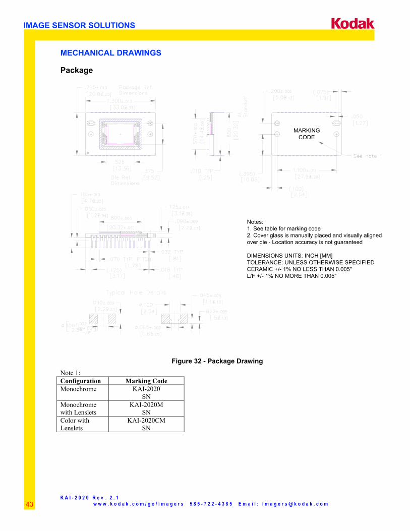
MECHANICAL DRAWINGS
Package
Notes:1. See table for marking code2. Cover glass is manually placed and visually alignedover die - Location accuracy is not guaranteed
DIMENSIONS UNITS: INCH [MM]TOLERANCE: UNLESS OTHERWISE SPECIFIEDCERAMIC +/- 1% NO LESS THAN 0.005"L/F +/- 1% NO MORE THAN 0.005"
MARKINGCODE
Figure 32 - Package Drawing
Note 1: Configuration Marking Code Monochrome KAI-2020
SN Monochrome with Lenslets
KAI-2020M SN
Color with Lenslets
KAI-2020CM SN
K A I - 2 0 2 0 R e v . 2 . 1 w w w . k o d a k . c o m / g o / i m a g e r s 5 8 5 - 7 2 2 - 4 3 8 5 E m a i l : i m a g e r s @ k o d a k . c o m
IMAGE SENSOR SOLUTIONS
44
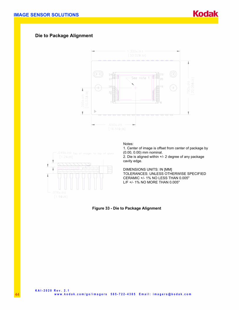
Die to Package Alignment
Notes:1. Center of image is offset from center of package by(0.00, 0.00) mm nominal.2. Die is aligned within +/- 2 degree of any packagecavity edge.
DIMENSIONS UNITS: IN [MM]TOLERANCES: UNLESS OTHERWISE SPECIFIEDCERAMIC +/- 1% NO LESS THAN 0.005"L/F +/- 1% NO MORE THAN 0.005"
Figure 33 - Die to Package Alignment
K A I - 2 0 2 0 R e v . 2 . 1 w w w . k o d a k . c o m / g o / i m a g e r s 5 8 5 - 7 2 2 - 4 3 8 5 E m a i l : i m a g e r s @ k o d a k . c o m
IMAGE SENSOR SOLUTIONS
45
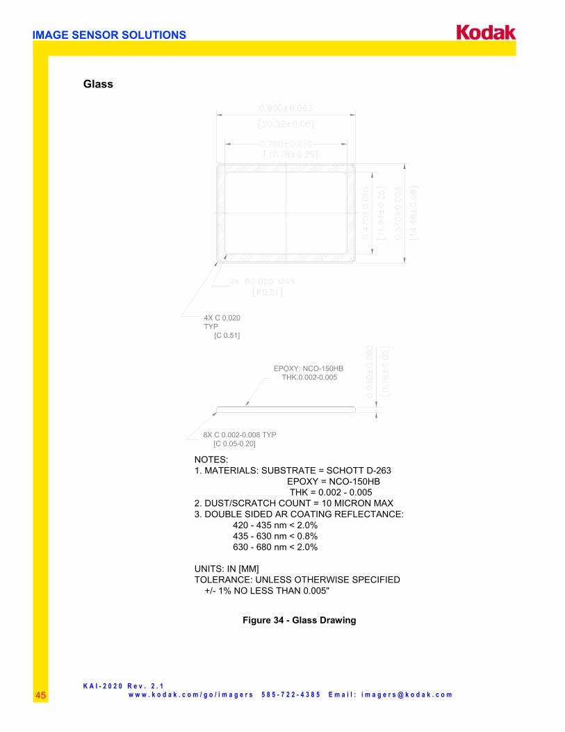
Glass
EPOXY: NCO-150HB THK.0.002-0.005
4X C 0.020TYP [C 0.51]
8X C 0.002-0.008 TYP [C 0.05-0.20]
NOTES:1. MATERIALS: SUBSTRATE = SCHOTT D-263 EPOXY = NCO-150HB THK = 0.002 - 0.0052. DUST/SCRATCH COUNT = 10 MICRON MAX3. DOUBLE SIDED AR COATING REFLECTANCE: 420 - 435 nm < 2.0% 435 - 630 nm < 0.8% 630 - 680 nm < 2.0%
UNITS: IN [MM]TOLERANCE: UNLESS OTHERWISE SPECIFIED +/- 1% NO LESS THAN 0.005"
Figure 34 - Glass Drawing
K A I - 2 0 2 0 R e v . 2 . 1 w w w . k o d a k . c o m / g o / i m a g e r s 5 8 5 - 7 2 2 - 4 3 8 5 E m a i l : i m a g e r s @ k o d a k . c o m
IMAGE SENSOR SOLUTIONS
46
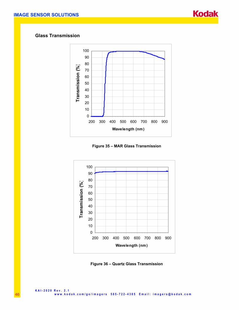
Glass Transmission
Figure 35 – MAR Glass Transmission
Figure 36 – Quartz Glass Transmission
0
10
2030
40
50
60
7080
90
100
200 300 400 500 600 700 800 900
Wavelength (nm)
Tran
smis
sion
(%)
0
10
20
30
40
5060
70
80
90
100
200 300 400 500 600 700 800 900
Wavelength (nm)
Tran
smis
sion
(%)

K A I - 2 0 2 0 R e v . 2 . 1 w w w . k o d a k . c o m / g o / i m a g e r s 5 8 5 - 7 2 2 - 4 3 8 5 E m a i l : i m a g e r s @ k o d a k . c o m
IMAGE SENSOR SOLUTIONS
47
QUALITY ASSURANCE AND RELIABILITY Quality Strategy: All image sensors will conform to the specifications stated in this document. This will be accomplished through a combination of statistical process control and inspection at key points of the production process. Typical specification limits are not guaranteed but provided as a design target. For further information refer to ISS Application Note MTD/PS-0292, Quality and Reliability. Replacement: All devices are warranted against failure in accordance with the terms of Terms of Sale. This does not include failure due to mechanical and electrical causes defined as the liability of the customer below. Liability of the Supplier: A reject is defined as an image sensor that does not meet all of the specifications in this document upon receipt by the customer. Liability of the Customer: Damage from mechanical (scratches or breakage), electrostatic discharge (ESD) damage, or other electrical misuse of the device beyond the stated absolute maximum ratings, which occurred after receipt of the sensor by the customer, shall be the responsibility of the customer. ESD Precautions: Devices are shipped in static-safe containers and should only be handled at static-safe workstations. See ISS Application Note MTD/PS-0224, Electrostatic Discharge Control, for handling recommendations. Reliability: Information concerning the quality assurance and reliability testing procedures and results are available from the Image Sensor Solutions and can be supplied upon request. For further information refer to ISS Application Note MTD/PS-0292, Quality and Reliability. Test Data Retention: Image sensors shall have an identifying number traceable to a test data file. Test data shall be kept for a period of 2 years after date of delivery. Mechanical: The device assembly drawing is provided as a reference. The device will conform to the published package tolerances.
K A I - 2 0 2 0 R e v . 2 . 1 w w w . k o d a k . c o m / g o / i m a g e r s 5 8 5 - 7 2 2 - 4 3 8 5 E m a i l : i m a g e r s @ k o d a k . c o m
IMAGE SENSOR SOLUTIONS
48
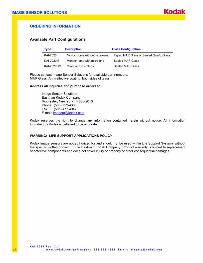
ORDERING INFORMATION
Available Part Configurations
Type Description Glass Configuration
KAI-2020 Monochrome without microlens Taped MAR Glass or Sealed Quartz Glass
KAI-2020M Monochrome with microlens Sealed MAR Glass
KAI-2020CM Color with microlens Sealed MAR Glass Please contact Image Sensor Solutions for available part numbers. MAR Glass: Anti-reflective coating, both sides of glass. Address all inquiries and purchase orders to:
Image Sensor Solutions Eastman Kodak Company Rochester, New York 14650-2010 Phone: (585) 722-4385 Fax: (585) 477-4947 E-mail: [email protected]
Kodak reserves the right to change any information contained herein without notice. All information furnished by Kodak is believed to be accurate. WARNING: LIFE SUPPORT APPLICATIONS POLICY Kodak image sensors are not authorized for and should not be used within Life Support Systems without the specific written consent of the Eastman Kodak Company. Product warranty is limited to replacement of defective components and does not cover injury or property or other consequential damages.
K A I - 2 0 2 0 R e v . 2 . 1 w w w . k o d a k . c o m / g o / i m a g e r s 5 8 5 - 7 2 2 - 4 3 8 5 E m a i l : i m a g e r s @ k o d a k . c o m
IMAGE SENSOR SOLUTIONS
49
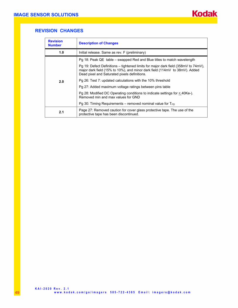
REVISION CHANGES
Revision Number Description of Changes
1.0 Initial release. Same as rev. F (preliminary)
2.0
Pg 18: Peak QE table – swapped Red and Blue titles to match wavelength
Pg 19: Defect Definitions – tightened limits for major dark field (358mV to 74mV), major dark field (15% to 10%), and minor dark field (114mV to 38mV). Added Dead pixel and Saturated pixels definitions.
Pg 26: Test 7: updated calculations with the 10% threshold
Pg 27: Added maximum voltage ratings between pins table
Pg 28: Modified DC Operating conditions to indicate settings for < 40Ke-). Removed min and max values for GND
Pg 30: Timing Requirements – removed nominal value for TFD
2.1 Page 27: Removed caution for cover glass protective tape. The use of the protective tape has been discontinued.