kurenai : kyoto university research information...
TRANSCRIPT

Title Studies on The Giant Magnetoresistance in MagneticSuperlattices( Dissertation_全文 )
Author(s) Suzuki, Motofumi
Citation Kyoto University (京都大学)
Issue Date 1998-03-23
URL https://doi.org/10.11501/3135659
Right
Type Thesis or Dissertation
Textversion author
Kyoto University

Studies on
The Giant Magnetoresistancein
Magnetic Superlattices
Motofumi Suzuki
1997

Acknowledgment
I would like to express my sincere gratitude to Professor Michi-hiko Mannamiof Kyoto University for the guidance, constructive suggestions, discussionsand encouragement throughout this study.
I would also like to thank Professor Masayuki Shiga and Professor TakashiFujimoto of Kyoto University for their critical suggestion and reading.
I am especially indebted to Dr. Yasunori Taga of TOYOTA Central Re-search and Development Laboratories, Inc. (TCRDL) for his continuous sup-port, valuable discussions, advises and encouragement over the period of thisstudy.
I would like to acknowledge Professor Hiroshi Yasuoka and Dr. AtushiGoto of Institute of Solid State Physics of University of Tokyo for usefuldiscussions and the support for NMR measurements.
I wish to thank members of Special Research Laboratory in TCRDL.I would like to my sincere thanks to Dr. Takeshi Ohwaki and Mr. KengoIshiyama for their useful discussions and advises. The skilled technical assis-tance and advises provided by Ms. Yuko Aoki, Ms. Atuko Inoue, Mr. AtsushiMiura, Mr. Takahiro Shiga and other members are also appreciated. Withouttheir helps, this work could not be completed.
I am grateful to Dr. Akira Hosono of TCRDL for their support for thisstudy and giving me the opportunity to prepare this thesis.
I would like to express my gratitude to Dr. Osami Kamigaito and Dr. Ri-ichi Takahashi of TCRDL for giving me a excellent circumstance and chanceto prepare this thesis.
Finally, I wish deeply to express my appreciation to my wife Miho andour parents for their encouragement throughout of this study. This thesis isdedicated to Miho and my son Kai.
iii

Contents
1 Introduction 1
1.1 Prior to discovery of GMR . . . . . . . . . . . . . . . . . . . . 2
1.2 GMR and AF coupling in magnetic superlattices . . . . . . . . 4
1.3 Origin of the GMR . . . . . . . . . . . . . . . . . . . . . . . . 7
1.4 Outline . . . . . . . . . . . . . . . . . . . . . . . . . . . . . . . 9
References . . . . . . . . . . . . . . . . . . . . . . . . . . . . . . . . 11
2 Experiments 17
Abstract . . . . . . . . . . . . . . . . . . . . . . . . . . . . . . . . . 17
2.1 Preparation of Co/Cu superlattices . . . . . . . . . . . . . . . 18
2.2 Characterization . . . . . . . . . . . . . . . . . . . . . . . . . 19
2.2.1 Measurements of GMR and magnetization . . . . . . . 19
2.2.2 X-ray diffraction . . . . . . . . . . . . . . . . . . . . . 19
2.2.3 59Co NMR . . . . . . . . . . . . . . . . . . . . . . . . . 20
References . . . . . . . . . . . . . . . . . . . . . . . . . . . . . . . . 22
3 Role of buffer layer in GMR 23
Abstract . . . . . . . . . . . . . . . . . . . . . . . . . . . . . . . . . 23
3.1 Introduction . . . . . . . . . . . . . . . . . . . . . . . . . . . . 24
3.2 Experiments . . . . . . . . . . . . . . . . . . . . . . . . . . . . 24
3.3 Results and discussion . . . . . . . . . . . . . . . . . . . . . . 25
3.3.1 Relationship between GMR and thicknesses of Co andCu . . . . . . . . . . . . . . . . . . . . . . . . . . . . . 25
3.3.2 Critical thickness of Fe buffer layer . . . . . . . . . . . 27
3.3.3 Dependence of GMR on substance of buffer layer . . . 32
3.4 Conclusion . . . . . . . . . . . . . . . . . . . . . . . . . . . . . 33
References . . . . . . . . . . . . . . . . . . . . . . . . . . . . . . . . 34
v

vi Contents
4 Interfacial structure of Co/Cu superlattices 37Abstract . . . . . . . . . . . . . . . . . . . . . . . . . . . . . . . . . 374.1 Introduction . . . . . . . . . . . . . . . . . . . . . . . . . . . . 384.2 Experiment . . . . . . . . . . . . . . . . . . . . . . . . . . . . 394.3 Results and discussion . . . . . . . . . . . . . . . . . . . . . . 40
4.3.1 XRD . . . . . . . . . . . . . . . . . . . . . . . . . . . . 404.3.2 NMR . . . . . . . . . . . . . . . . . . . . . . . . . . . . 45
4.4 Conclusion . . . . . . . . . . . . . . . . . . . . . . . . . . . . . 51References . . . . . . . . . . . . . . . . . . . . . . . . . . . . . . . . 52
5 GMR in Co/Cu superlattices with mixed interfaces I 57Abstract . . . . . . . . . . . . . . . . . . . . . . . . . . . . . . . . . 575.1 Introduction . . . . . . . . . . . . . . . . . . . . . . . . . . . . 585.2 Experiment . . . . . . . . . . . . . . . . . . . . . . . . . . . . 595.3 Results and discussion . . . . . . . . . . . . . . . . . . . . . . 595.4 Conclusion . . . . . . . . . . . . . . . . . . . . . . . . . . . . . 66References . . . . . . . . . . . . . . . . . . . . . . . . . . . . . . . . 67
6 GMR in Co/Cu superlattices with mixed interfaces II 69Abstract . . . . . . . . . . . . . . . . . . . . . . . . . . . . . . . . . 696.1 Introduction . . . . . . . . . . . . . . . . . . . . . . . . . . . . 706.2 Experiment . . . . . . . . . . . . . . . . . . . . . . . . . . . . 716.3 Results and discussion . . . . . . . . . . . . . . . . . . . . . . 72
6.3.1 Relationship between GMR and magnetization . . . . . 726.3.2 Temperature dependence of GMR . . . . . . . . . . . . 78
6.4 Conclusion . . . . . . . . . . . . . . . . . . . . . . . . . . . . . 84References . . . . . . . . . . . . . . . . . . . . . . . . . . . . . . . . 85
7 Influence of bound d state on GMR 89Abstract . . . . . . . . . . . . . . . . . . . . . . . . . . . . . . . . . 897.1 Introduction . . . . . . . . . . . . . . . . . . . . . . . . . . . . 907.2 Model . . . . . . . . . . . . . . . . . . . . . . . . . . . . . . . 917.3 Superlattice state for d band . . . . . . . . . . . . . . . . . . . 947.4 Calculation of resistivity . . . . . . . . . . . . . . . . . . . . . 95
7.4.1 s–s scattering . . . . . . . . . . . . . . . . . . . . . . . 967.4.2 s–d scattering . . . . . . . . . . . . . . . . . . . . . . . 97
7.5 GMR . . . . . . . . . . . . . . . . . . . . . . . . . . . . . . . . 997.6 Interfacial scattering in Co/Cu . . . . . . . . . . . . . . . . . . 1027.7 Conclusion . . . . . . . . . . . . . . . . . . . . . . . . . . . . . 106References . . . . . . . . . . . . . . . . . . . . . . . . . . . . . . . . 107

Contents vii
8 GMR sensors using Co/Cu superlattices 111Abstract . . . . . . . . . . . . . . . . . . . . . . . . . . . . . . . . . 1118.1 Introduction . . . . . . . . . . . . . . . . . . . . . . . . . . . . 1128.2 Experiments . . . . . . . . . . . . . . . . . . . . . . . . . . . . 1138.3 Results and discussion . . . . . . . . . . . . . . . . . . . . . . 117
8.3.1 Refinement of Co/Cu superlattices . . . . . . . . . . . 1178.3.2 Characteristics of GMR sensors . . . . . . . . . . . . . 1188.3.3 Thermal durability of GMR sensors . . . . . . . . . . . 123
8.4 Conclusion . . . . . . . . . . . . . . . . . . . . . . . . . . . . . 126References . . . . . . . . . . . . . . . . . . . . . . . . . . . . . . . . 127
List of Publications 129


Chapter 1
Introduction
1
2 Chapter 1. Introduction
This thesis is on the studies on the giant magnetoresistance (GMR) in
Co/Cu superlattices. The transport properties of Co/Cu superlattices have
been experimentally investigated with the special emphasis on the relation-
ship between the magnetoresistance (MR) and the superlattices structures,
which include the crystallographic, long- and short-range interfacial rough-
ness. The theoretical model consistent with the experimental results has
been also proposed. Furthermore, we have demonstrated the usefulness of
the GMR in Co/Cu superlattices for the practical application to the magnetic
rotation sensor.
In this chapter, brief introduction to the GMR in metallic multilayers and
the outline of this thesis are described.
1.1 Prior to discovery of GMR
The physical properties of the artificial nanostructured materials have been
studied since a hundred years ago. The optical properties of the metallic
fine particles embedded in the dielectric materials were initiated at the be-
ginning of this century by Maxwell Garnett [1, 2], and are still active in the
various field in present [3]. Although, the studies on the artificial multilay-
ered materials prepared by vacuum deposition also have a long history, the
vacuum condition before 1960’s was not heigh enough to produce reliable
samples. Around 1970, ultra high vacuum techniques have been introduced
in the field of material fabrication, studies on the semiconductor superlattices
were initiated by Esaki’s group [4]. Recently, even a monolayer–monolayer
superlattices of GaAs/AlAs has been successfully synthesized [5].
On the other hand, it is past 1980’s that significant developments in the
1.1. Prior to discovery of GMR 3
research on physical properties of metallic superlattices have been made,
although x-ray optics of the metallic multilayers were investigated before
1960’s. Prior to the discovery of the GMR, most researchers have focused
their attention on the magnetism and the superconductivity among the fun-
damental physical properties of metallic superlattices, since the superlattices
are useful to investigate magnetic anomalies at interfaces and properties of
two-dimensional magnetic systems. In these studies, many interesting phe-
nomena have been found such as the enhancement of the magnetic moment
of Ni atoms at interfaces between Ni and Cu [6, 7] and perpendicular mag-
netization in Co/Pd superlattices [8].
The peculiar magnetic structure in Fe/Cr/Fe sandwich films found by
Grunberg et al. in 1986 is one of the most important discovery in the studies
on the metallic superlattices [9]. They found the strong antiferromagnetic
(AF) coupling between two ferromagnetic (F) Fe layers. Due to the AF
coupling, magnetization of Fe layers align antiparallel in the weak magnetic
field, while they align parallel in the stronger field than the saturation. They
also measured the magnetoresistance (MR) in these sandwich films. Unfortu-
nately, measured MR ratio, which is the relative change in resistivity, is less
than 1 %, so that this work did not attract the attention from the standpoint
of the MR effect. However, it is clear that this work is on the frontiers of the
discovery of GMR.

4 Chapter 1. Introduction
1.2 GMR and AF coupling in magnetic su-
perlattices
Following the work of Grunberg et al., Fert’s group have prepare Fe/Cr su-
perlattices, and have measured transport properties [10]. As the results, it
has been found that the resistance in [Fe(3.0 nm)/Cr(0.9 nm)]n (n = 60)
superlattice at 0 field decreases down to the half value at the magnetic field
of 20 kOe as shown in Fig. 1.1, where the subscript n indicates the number
of bilayers in the sample. This is the first report on the GMR in magnetic su-
perlattices and made a great impact on the fundamental and applied physics.
Since the samples with large MR ratio had the small remanence magnetiza-
tion, they considered that the magnetization of the adjacent Fe layers aligned
antiparallel in the weak magnetic field due to the strong AF interlayer cou-
pling, while the magnetization of Fe layers aligned parallel in the magnetic
field large enough to predominate over the AF coupling. In Fig. 1.1, pro-
posed configuration of the magnetization of Fe layers is indicated. In fact,
the AF alignment was confirmed immediately by neutron diffraction [11].
Relating to the change in the magnetic structure, the GMR is understood
phenomenologically as follows: In the ferromagnetic metals, the current is
carried separately by up- and down-spin conduction electrons (two-current
model) as [12]
ρ =ρ↑ρ↓
ρ↑ + ρ↓, (1.1)
where ρ↑ and ρ↓ are the resistivity of up- and down-spin channels, respec-
tively, and ρ is the total resistivity. Moreover, it is known that the scattering
of conduction electrons can be strongly spin dependent in a ferromagnetic

1.2. GMR and AF coupling in magnetic superlattices 5
0.6
0.7
0.8
1.0
-40 -20 0 20 40
R/R(H=0)
Magnetic field (kOe)
Fig. 1.1: Magnetoresistance of the Fe/Cr superlattice at 4.2 K [10].The current and the applied field are in the plane of the layers. Allowsindicate the schematic configuration of the magnetization of Fe layers.
transition metal (ρ↑ ρ↓ or ρ↑ ρ↓). In the superlattices in ferromagnetic
(F) alignment, electrons of one spin direction always travel in the channel
of small resistivity, while electrons of another spin direction travel in the
channel of large resistivity. On the other hand, in the superlattices in AF
alignment, electrons of both spin directions alternately travel in the channels
of small and large resistivity. Therefore, total resistivity for F alignment
becomes much smaller than that for AF alignment.

6 Chapter 1. Introduction
The discovery of the GMR in magnetic superlattices raised two questions
on the origins of the AF interlayer coupling and the mechanism of the spin-
dependent conduction electron scattering. These problems have attracted
much attention from both fundamental and practical standpoints. Other
than the Fe/Cr superlattices, the GMR and the AF interlayer coupling have
been observed in the various systems such as Co/Cu [13, 14], NiFe/Cu [15],
CoFe/Cu [16] and Co/Ag [17]. Especially the transition metal/Cu systems
are significant for the practical application to the MR sensors, since their
MR ratio is considerably large even at room temperature, and the saturation
field is small. Moreover, Parkin et al. reported remarkable results on the
GMR and the interlayer coupling in superlattices [14, 18]. They measured
the MR ratio and the magnetization curves as a function of the thickness
of the nonmagnetic layer, so that the magnitude of the MR ratio and the
saturation field were found to oscillate with the nonmagnetic layer thickness
with a period of 10–15 A (see Fig 3.1 in Chapter 3). This oscillation has been
attributed to that the interlayer exchange coupling between the adjacent
magnetic layers oscillates between F and AF coupling as a function of the
nonmagnetic layer thickness. According to this interpretation, the interlayer
exchange coupling plays an important role in the GMR in superlattices.
For the GMR, however, the interlayer coupling is not essential, but the
AF alignment of the magnetization of the adjacent magnetic layers is. In
fact, Shinjo and Yamamoto reported the GMR in the superlattices in which
the adjacent magnetic layers were not coupled [19]. They prepared a super-
lattice of [Co(30 A)/Cu(50 A)/NiFe(30 A)/Cu(50 A)]15. In this superlattice,
AF alignment of the magnetization was achieved by the difference in the co-

1.3. Origin of the GMR 7
ercive force of two magnetic layers, since Co and NiFe are magnetically hard
and soft materials, respectively. Another uncoupled sandwich structure, the
so-called spin valve, is proposed as the sensitive GMR system [20–23]. In
the spin valve structure, the magnetization of magnetic layers is aligned an-
tiferromagnetically by pinning the magnetization of one of the ferromagnetic
layers using the exchange-biasing layer. Therefore, the GMR and the inter-
layer exchange coupling are the problems independent of each other. The
theme of this thesis is the GMR in Co/Cu superlattices, so that we will not
enter into detailed discussions on the interlayer exchange coupling.
1.3 Origin of the GMR
The origin of the GMR can be attributed to the spin-dependent scatter-
ing of conduction electrons as described in the previous section. However,
mechanism of the spin-dependent scattering still remains unclear. Many
experimental studies deal with the correlation between the GMR and the in-
terfacial roughness to understand the role of interfaces [15,24–27]. For Fe/Cr
superlattices [24, 25], the enhancement of both the magnitude and tempera-
ture dependence of the GMR due to interfacial roughness has been reported,
so that the origin of the GMR in Fe/Cr is attributed to the interfacial scat-
tering [28]. However, for transition metal (M)/Cu superlattices, no one has
reported that the interfacial roughness enhances the GMR [15, 26, 27]. This
suggests that the spin-dependent bulk scattering is important for the occur-
rence of the GMR. Nevertheless, the importance of interfacial scattering has
been pointed out indirectly in studies on the layer thickness dependence of
the GMR [29, 30]. Parkin [29] has reported that the GMR is enhanced by
8 Chapter 1. Introduction
very thin Co layers inserted at interfaces of NiFe/Cu multilayers. He claimed
that the interfacial state as well as roughness plays an important role in the
GMR. These experimental results require a theory to take account of both
the spin-dependent bulk scattering and the interfacial electronic states.
On the other hand, there are many theoretical studies discussing the ori-
gin of the GMR. Camley and Barnas [31, 32] have proposed a semi-classical
model for the GMR by extending the Fuchs-Sondheimer model [33, 34]. In
their model, the GMR is described with many phenomenological parame-
ters for conduction electrons such as spin-dependent mean free paths in lay-
ers, reflection, transmission and diffuse scattering coefficients at interfaces.
Quantum mechanical models by Hood and Falicov [35] and by Visscher [36]
relate these phenomenological parameters to superlattice potentials and the
potentials of bulk and interfacial scatterers. Since these theories are based
on a single band free electron model, spin-dependent scattering is attributed
to spin-dependent potentials. For Fe/Cr superlattices, the spin-dependent
potentials due to interfacial roughness have been indicated by microscopic
theories [37–39].
In discussing the GMR inM/Cu, however, the above theories are not ap-
propriate, since they do not include the information about the band structure
being very different from that of Fe/Cr. If we take account of the electronic
band structure, the formalism for the bulk and interfacial scattering will be
modified. For M/Cu systems, Edwards et al. [40] claimed in their resistor
network theory that the spin-dependent s–d scattering in bulk is the domi-
nant process giving arise to the GMR. Xing et al. [41, 42] also insist on the
importance of spin-dependent density of states (DOS) of d bands in magnetic

1.4. Outline 9
layers. In these models, the GMR is attributed to the scattering of s electrons
into unfilled d bands which have spin-dependent DOS. These models semi-
quantitatively agree with the layer thickness dependence of GMR in M/Cu
systems. However, the influence of the interfacial state has not been treated
explicitly, since the Fermi surfaces of s and d bands are treated as simple
spheres. Recently, Schep et al. [43] calculated the GMR in a method based
on the full electronic structure. They reported the importance of the s–d
hybridization for the origin of the GMR in the current-perpendicular-to-the-
plane (CPP) geometry. However, their theory does not satisfactorily explain
the considerable MR observed in the current-in-the-plane (CIP) geometry.
They suggest that some additional scattering mechanism is necessary for ex-
plaining the CIP MR. The mechanism of the GMR in M/Cu superlattices
still remains unclear.
In this thesis, we discuss the origin of the GMR in Co/Cu superlat-
tices based on the experimental data for the Co/Cu superlattices with well-
controlled interfacial roughness and the theoretical s–d scattering model tak-
ing account of the interfacial states.
1.4 Outline
The outline of this thesis is as follows:
Chapter 2 describes the experimental methods; preparation of samples
and the structural analysis by using the x-ray diffraction and the NMR.
In Chapter 3, the characteristic features of the GMR and the structures
of Co/Cu superlattices deposited on various buffer layers are surveyed. A
drastic changes in the MR ratio and the saturation field are found, depending

10 Chapter 1. Introduction
on the thickness and the substance of the buffer layer. The strong correlation
between the GMR and the structures is discussed briefly.
In Chapter 4, an attempt is made to clarify the effect of interfacial mix-
ing on the x-ray diffraction (XRD) and 59Co NMR of Co/Cu superlattices.
Systematic and quantitative modification of interfaces has been achieved by
codeposition of Co and Cu at interfaces. We show that high and low angle
XRD patterns are not affected by the existence of compositionally mixed
regions thinner than 0.3 nm, and that significant change in the distribution
of hyperfine field of 59Co is found.
In Chapter 5 and 6, the detailed GMR and magnetic properties of the
Co/Cu superlattices with intentionally mixed interfaces are shown. The re-
sults are discussed using the spin-split DOS model of Xing et al. [41, 42].
The magnetization dependence of the GMR has precluded the existence of a
strong spin dependence in the potential not only for the bulk but also for the
interfacial scattering. The temperature dependence of the GMR is hardly
influenced by the interfacial roughness, while the residual resistivity changes
significantly. This reveals that the spin-dependent s–d scattering in the bulk
is crucial for the GMR in Co/Cu superlattices. The interfacial roughness
mainly contributes to the residual resistivity, and the spin dependence in the
scattering at interfaces is weaker than that in the bulk.
In Chapter 7, we discuss theoretically the GMR in magnetic superlattices
with an s–d scattering model on the assumption that d states are bound in
magnetic layers. The GMR is calculated by using the quantum Boltzmann
equation using Kronig-Penney type potentials. Spin-dependent interfacial
scattering depends on the number of scatterers, the height of the scatter-
References 11
ing potentials and the amplitude of the wave function of the d state at
interfaces, while spin-dependent bulk scattering is attributed to the spin-
dependent DOS of d states. Our model agrees well with the measured GMR
in Co/Cu superlattices with artificially mixed interfaces, when we assume
that the minority spin d states are strongly bound in Co layers. Therefore,
the spin-dependent scattering in Co/Cu superlattices is attributed to the
spin-dependent DOS of the d states in the Co layers.
Finally, in Chapter 8, we demonstrate the usefulness of the GMR in
Co/Cu superlattices for the practical application to the magnetic rotation
sensor. Optimized Co/Cu superlattices have been fabricated into the sensors
with appropriate passivation layers. The sensor output changes more than
20% synchronizing the rotation of magnet rotor. It is remarkable that the
degradation of the GMR sensors is not significant even after the sensors are
left in air at 150 C for 1000 h. This confirms the high reliability of the GMR
sensors and promises us that the GMR sensors can be used in automobiles
and aircraft under the sever conditions.
References
[1] J. C. Maxwell Garnett, Philos. Trans. R. Soc. London, Ser. A 203, 385
(1904).
[2] J. C. Maxwell Garnett, Philos. Trans. R. Soc. London, Ser. A 205, 237
(1906).
[3] M. Suzuki and Y. Taga, J. Appl. Phys. 71, 2848 (1992).
12 Chapter 1. Introduction
[4] P. Voisin, G. Bastard, C. E. T. Goncalves da Silva, M. Voos, L. L.
Chang, and L. Esaki, Solid State Commun. 39, 79 (1981).
[5] H. Terauchi, S. Sekimoto, K. Kamigaki, H. Sakashita, N. Sano, H. Kato,
and M. Nakayama, J. Phys. Soc. Jpn. 54, 4576 (1985).
[6] B. J. Thaler and J. B. Ketterson, Phys. Rev. Lett. 41, 336 (1978).
[7] E. M. Gyorgy, D. B. McWhan, J. E. Dillon Jr., L. R. Walker, and J. V.
Waszczak, Phys. Rev. B 25, 6739 (1982).
[8] P. F. Carcia, A. D. Meinhaldt, and A. Suna, Appl. Phys. Lett. 47, 178
(1985).
[9] P. Grunberg, R. Schreiber, Y. Pang, M. B. Brodsky, and H. Sower, Phys.
Rev. Lett. 57, 2442 (1986).
[10] M. N. Baibich, J. M. Broto, A. Fert, F. Nguyen Van Dau, F. Petroff, P.
Etienne, G. Creuzet, A. Friederich, and J. Chazelas, Phys. Rev. Lett.
61, 2472 (1988).
[11] N. Hosoito, S. Araki, K. Mibu, and T. Shinjo, J. Phys. Soc. Jpn. 59,
1925 (1990).
[12] A. Fert and I. A. Campbell, J. Phys. C 6, 849 (1976).
[13] D. H. Mosca, F. Petroff, A. Fert, P. A. Schroeder, W. P. Pratt Jr., and
R. Laloee, J. Magn. Magn. Mater. 94, L1 (1991).
[14] S. S. P. Parkin, R. Bhadra, and K. P. Roche, Phys. Rev. Lett. 66, 2152
(1991).

References 13
[15] V. S. Speriosu, J. P. Nozieres, B. A. Gurney, B. Dieny, T. C. Huang,
and H. Lefakis, Phys. Rev. B 47, 11579 (1993).
[16] Y. Saito, S. Hashimoto, and K. Inomata, Appl. Phys. Lett. 60, 2436
(1992).
[17] W. P. Pratt Jr., S. F. Lee, J. M. Slaughter, R. Loloee, P. A. Schroeder,
and J. Bass, Phys. Rev. Lett. 66, 3060 (1991).
[18] S. S. P. Parkin, N. More, and K. P. Roche, Phys. Rev. Lett. 64, 2304
(1990).
[19] T. Shinjo and H. Yamamoto, J. Phys. Soc. Jpn. 59, 3061 (1990).
[20] B. Dieny, V. S. Speriosu, S. S. P. Parkin, B. A. Gurney, D. R. Wilhoit,
and D. Mauri, Phys. Rev. B 43, 1297 (1991).
[21] B. Dieny, V. S. Speriosu, S. Metin, S. S. P. Parkin, B. A. Gurney, P.
Baumgart, and D. R. Wilhoit, J. Appl. Phys. 69, 4774 (1991).
[22] A. Chaiken, P. Lubitz, J. J. Krebs, G. A. Prinz, and M. Z. Harford,
Appl. Phys. Lett. 59, 240 (1991).
[23] A. Chaiken, P. Lubitz, J. J. Krebs, G. A. Prinz, and M. Z. Harford, J.
Appl. Phys. 70, 5864 (1991).
[24] F. Petroff, A. Barthelemy, A. Hamzic, A. Fert, P. Etienne, S. Lequien,
and G. Creuzet, J. Magn. Magn. Mater. 93, 95 (1991).
[25] E. E. Fullerton, D. M. Kelly, J. Guimpel, I. K. Schuller, and Y. Bruynser-
aede, Phys. Rev. Lett. 68, 859 (1992).

14 Chapter 1. Introduction
[26] M. J. Hall, B. J. Hickey, M. A. Howson, C. Hammond, M. J. Walker,
D. G. Wright, D. Greig, and N. Wiser, J. Phys. Condens. Mater. 4, L495
(1992).
[27] Y. Saito, K. Inomata, A. Goto, and H. Yasuoka, J. Phys. Soc. Jpn. 62,
1450 (1993).
[28] S. Zhang and P. M. Levy, Phys. Rev. B 43, 11048 (1991).
[29] S. S. P. Parkin, Phys. Rev. Lett. 71, 1641 (1993).
[30] S. K. J. Lenczowski, M. A. M. Gijs, J. B. Geisbers, R. J. M. van de
Veerdonk, and W. J. M. de Jonge, Phys. Rev. B 50, 9982 (1994).
[31] R. E. Camley and J. Barnas, Phys. Rev. Lett. 63, 664 (1989).
[32] J. Barnas, A. Fuss., R. E. Camley, P. Grunberg, and W. Zinn, Phys.
Rev. B 42, 8110 (1990).
[33] K. Fuchs, Proc. Cambridge Philos. Soc. 34, 100 (1938).
[34] E. H. Sondheimer, Adv. Phys. 1, 1 (1952).
[35] R. Q. Hood and L. M. Falicov, Phys. Rev. B 46, 8287 (1992).
[36] P. B. Visscher, Phys. Rev. B 49, 3907 (1994).
[37] P. M. Levy, S. Zhang, and A. Fert, Phys. Rev. Lett. 65, 1643 (1990).
[38] P. M. Levy, S. Zhang, and A. Fert, Phys. Rev. B 45, 8689 (1992).
[39] J. Inoue, A. Oguri, and S. Maekawa, J. Phys. Soc. Jpn. 60, 376 (1991).

References 15
[40] D. M. Edwards, J. Mathon, and R. B. Muniz, IEEE Trans. Magn. 27,
3548 (1991).
[41] L. Xing and Y. C. Chang, Phys. Rev. B 48, 4156 (1993).
[42] L. Xing, Y. C. Chang, M. B. Salamon, D. M. Frenkel, J. Shi, and J. P.
Lu, Phys. Rev. B 48, 6728 (1993).
[43] K. M. Schep, P. J. Kelly, and G. E. W. Bauer, Phys. Rev. Lett. 74, 586
(1995).


Chapter 2
Experiments
Abstract
In this chapter, we describe the experimental methods; preparationof samples and the structural analysis by using the x-ray diffractionand NMR.
17
18 Chapter 2. Experiments
substrate holder
T1
T2 T3
S3S2
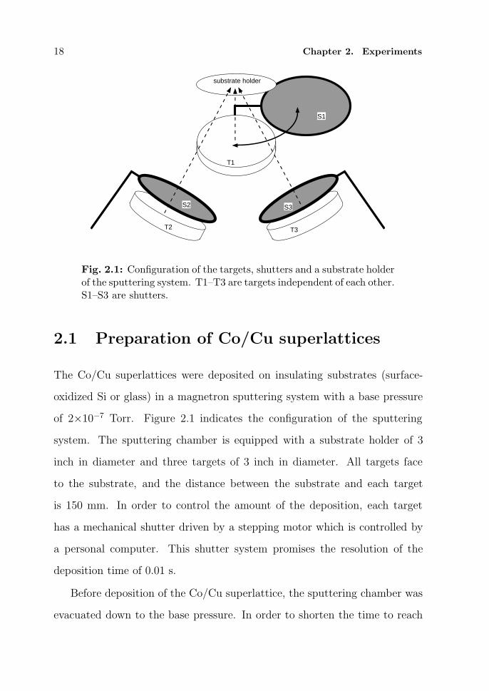
S1
Fig. 2.1: Configuration of the targets, shutters and a substrate holderof the sputtering system. T1–T3 are targets independent of each other.S1–S3 are shutters.
2.1 Preparation of Co/Cu superlattices
The Co/Cu superlattices were deposited on insulating substrates (surface-
oxidized Si or glass) in a magnetron sputtering system with a base pressure
of 2×10⁻⁷ Torr. Figure 2.1 indicates the configuration of the sputtering
system. The sputtering chamber is equipped with a substrate holder of 3
inch in diameter and three targets of 3 inch in diameter. All targets face
to the substrate, and the distance between the substrate and each target
is 150 mm. In order to control the amount of the deposition, each target
has a mechanical shutter driven by a stepping motor which is controlled by
a personal computer. This shutter system promises the resolution of the
deposition time of 0.01 s.
Before deposition of the Co/Cu superlattice, the sputtering chamber was
evacuated down to the base pressure. In order to shorten the time to reach
2.2. Characterization 19
the base pressure, the sputtering chamber was baked at 100 C for 2.5 h
and then cooled to room temperature. Immediately before the deposition,
substrate surface was cleaned by rf sputtering at 1 W/cm2 for 4 min in an
Ar pressure of 3×10⁻³ Torr. These processes are important to obtain Co/Cu
superlattices with a lage MR ratio.
In most cases, we deposited a metal buffer layer between the substrate
and the superlattice. After deposition of a buffer layer, 16–24 Co/Cu bilayers
were grown at room temperature in an Ar pressure of 3×10⁻³ Torr at a
deposition rate of 0.2–0.3 nm/s.
2.2 Characterization
2.2.1 Measurements of GMR and magnetization
The in-plane magnetoresistance (MR) was measured with a standard dc four-
terminal geometry. The magnetization was also measured with a supercon-
ducting quantum interface device (SQUID) magnetometer.
2.2.2 X-ray diffraction
Using a conventional powder diffractometer, high and low angle x-ray diffrac-
tion (XRD) measurements were performed in a symmetrical reflection(θ−2θ)geometry to characterize the crystallographic structure and the periodicity
of superlattices. The divergence of the incident Co Kα radiation (λ = 0.179
nm) was 1 for high angle XRD and 1/6 for low angle XRD. The scattered
x-ray was detected with a proportional counter, after the Co Kβ radiation
was eliminated with a graphite monochromator. Since we used a bright x-ray
source and the dynamic range of the counter was not so high, the total reflec-

20 Chapter 2. Experiments
tion was not recorded in the low angle XRD. Thus, we could not deduce the
value of an x-ray reflectivity. Nevertheless, our samples for XRD were large
enough compared with the beam size of an x-ray, so that the reproducibil-
ity of diffraction patterns measured at 2θ≥2 was very good in the absolutevalue. This fact confirms that the measured intensity in our experiment was
proportional to the reflectivity of an x-ray.
2.2.3 59Co NMR
NMR experiments were carried out in zero field at liquid helium temperature.
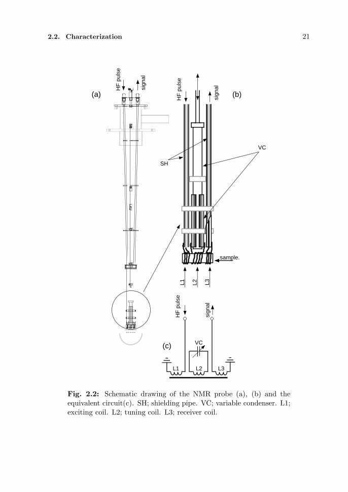
Figure 2.2 is the schematic drawing of the probe for the NMR measurement.
In order to apply the rf field and to detect the spin echo signal, three coils
of Cu wire of 1 mm in diameter are equipped at the bottom of the probe.
Two of them are excitation and receiver coils of two turns and another is the
tuning coil of three turns. The tuning coil is connected with the cylindrical
condenser of Cu and bakelite, and it is tuned to get impedance matching
between the exciting and receiver coils at each frequency. A sample was
divided into rectangular pieces of 10 × 20 mm2. Ten of them were stacked
up and were fitted into coils. Thus, the rf field of 5–10 W was applied
parallel to the film plane. Using a variable frequency spin-echo apparatus,
the distribution of the hyperfine field of 59Co was measured in a frequency
range of 120–240 MHz.
The frequency spectrum was obtained by plotting the spin-echo amplitude
at each frequency point by point. The pulse width and the separation of two
rf pulses were kept at constant values of 1.2 µs and 15 µs, respectively.
To obtain the number of atoms which resonate at a particular frequency
2.2. Characterization 21
(a) (b)
HF
pul
se
sign
al
sample.
L1 L2 L3
VC
HF
pul
se
sign
al
(c)
HF
pul
se
sign
al
L1 L2 L3
VC
SH
Fig. 2.2: Schematic drawing of the NMR probe (a), (b) and theequivalent circuit(c). SH; shielding pipe. VC; variable condenser. L1;exciting coil. L2; tuning coil. L3; receiver coil.

22 Chapter 2. Experiments
from the observed spin-echo amplitude, we collected the variation of the
Boltzmann factor (∝ ω) and the frequency dependence of the enhancement
effect of nuclear signals (∝ ω) [1]. Moreover, the frequency dependence of the
detected voltage induced by the processing magnetization (∝ ω) should be
took into account. Thus, the spin-echo amplitude divided by ω3 was taken
to be proportional to the number of nuclei with a given resonance frequency.
If the reference signal together with the spin echo signal was measured, the
ω2 dependence of the spin-echo amplitude was corrected.
References
[1] H. Yasuoka, in Metallic Superlattices, edited by T. Shinjo and T. Takada
(Elsevier, Amsterdam, 1987), p. 159.

Chapter 3
Role of buffer layer in GMR
Abstract
The giant magnetoresistance (GMR) in the Co/Cu superlatticesdeposited on the various buffer layers has been investigated. A drasticchanges in the MR ratio and the saturation field are found, dependingon the thickness and the substance of the buffer layer. Changes in thecrystallinity and interfacial roughness are responsible for the behaviorof the GMR
23

24 Chapter 3. Role of buffer layer in GMR
3.1 Introduction
Much attention has been devoted to the giant magnetoresistance (GMR) and
antiferromagnetic coupling of several multilayered systems, such as Fe/Cr [1],
and Co/Cu [2, 3]. Among them, the largest MR ratio has been found in
(111) textured magnetron sputtered Co/Cu systems. The key to achieve
the large MR ratio was to insert an Fe buffer layer between Co/Cu and the
substrate [3, 4].
In this chapter, we report the investigation on the effect of the buffer layer
on the GMR property, crystallographic structures and interfacial roughness
of magnetron sputtered Co/Cu superlattices.
3.2 Experiments
The Co/Cu superlattices were deposited on surface-oxidized Si substrates in
a magnetron sputtering system with a base pressure of 2×10⁻⁷ Torr. After
deposition of a buffer layer, 16–24 Co/Cu bilayers were grown at room tem-
perature in an Ar pressure of 3×10⁻³ Torr at a deposition rate of 0.2 − 0.3
nm/s.
In order to find the best combination of the layer thickness of Co and
Cu, we prepared the Co/Cu superlattices on an Fe buffer layer of thickness
5.0 nm with various combination of thicknesses of Co (tCo) and Cu (tCu).
The number of bilayers of Co/Cu was chosen between 16 and 24 so that
the total thickness was kept larger than 50 nm for all samples in order to
reduce the effect of the spin-independent surface scattering. The in-plane
magnetoresistance (MR) was measured at room temperature with a stan-

3.3. Results and discussion 25
dard dc four-terminal geometry. The dimension of the samples used for this
measurement was 3×50 mm2, and the current used was 1 mA.
Using the optimized combination of tCo and tCu, we investigated the effect
of the substance and the thickness of the buffer layer. The substance of the
buffer layer was selected among Cr, Fe, Co, NiFe, NiCo, Cu and Pt, and its
thickness tM (M =Cr, Fe, Co, NiFe, NiCo, Cu, Pt) was varied between 0
and 15.0 nm.
The crystallographic structure of the sample was characterized by x-ray
diffraction, and the interfacial atomic structures were evaluated from the dis-
tribution of the hyperfine field associated with the Co atoms near interfaces.
To obtain the hyperfine field, we have employed 59Co NMR in zero field at
4.2 K using the variable frequency spin-echo apparatus.
3.3 Results and discussion
3.3.1 Relationship between GMR and thicknesses of
Co and Cu
The MR properties as a function of tCu and tCo are investigated for a series
of the samples with an Fe buffer layer of thickness 5.0 nm. As indicated in
Fig. 3.1, the MR ratio and the saturation field Hs oscillate as a function of
the Cu layer thickness and show peaks at tCu = 0.9±0.05 and tCu = 2.1±0.1nm. This is consistent with Refs. [2, 3]. The MR ratio and Hs at the first
peak are 45% and 6 kOe, respectively, whereas they are 33% and 1.0 kOe at
the second peak. Here, the MR ratio is defined as
MR ratio = (ρmax − ρs)/ρs = ∆ρ/ρs, (3.1)

26 Chapter 3. Role of buffer layer in GMR
0
10
20
30
40
50
0 1.0 2.0 3.0 4.0
MR
rat
io (
%)
layer thickness (nm)
t Cu
t Co
0
10
20
30
40
50
-10 -5 0 5 10
MR
rat
io (
%)
H (kOe)
0
10
20
30
40
50
-10 -5 0 5 10M
R r
atio
(%
)H (kOe)
(a)
(b) (c)
Fig. 3.1: (a) The layer thickness dependence of the GMR in Co/Cusuperlattices deposited on an Fe buffer layer of 5.0 nm. Solid circlesindicate the MR ratio for the samples of [Co(1.0 nm)/Cu(tCu nm)]n,and open circles indicates the MR ratio for the samples of [Co(tCo
nm)/Cu(2.0 nm)]n. (b) The MR curves for the samples of [Co(1.0nm)/Cu(0.9 nm)]24. (c) Those for [Co(1.0 nm)/Cu(2.2 nm)]16 (c) arealso indicated.

3.3. Results and discussion 27
where ρmax and ρs are the maximum and saturation resistivity, respectively.
On the other hand, as a function of the Co layer thickness, the MR ratio shows
a broad peak at around tCo = 1.0 nm. Since the MR ratio at around tCu = 0.9
nm is very sensitive to the Cu layer thickness, it is difficult to prepare samples
with almost identical GMR properties. Therefore, we focus our attention on
the MR properties at the second peak of the oscillatory property of the
GMR as a function of the Cu layer thickness. The structure of the Co/Cu
superlattices discussed here is as follows: substrate/buffer layer/Cu(2.1±0.1nm)/[Co(1.0± 0.2 nm)/Cu(2.1± 0.1 nm)/]16.
3.3.2 Critical thickness of Fe buffer layer
The variation of the saturation MR ratio and the x-ray diffraction intensity
of the (111), (200) and (220) as a function of tFe is shown in Fig. 3.2. The
x-ray diffraction intensity is normalized by the relative intensity of powder
diffraction of fcc crystals. A drastic change in the MR ratio is found at
about tFe = 3.0 nm. The saturation field Hs also changes at tFe = 3.0 nm.
For tFe < 3.0, Hs is almost constant at 500 Oe, while it is also constant at 1
kOe for tFe ≥ 3.0.
The preferred orientation for the sample is also transformed suddenly
from (111) to (110) at the critical Fe buffer layer thickness of 3.0 nm as
shown in Fig. 3.2(b). Obviously, there exists a strong correlation between
the MR values and the textured structures. The size of grains with each
texture estimated from FWHM of (111), (200) and (220) diffraction peak
is about 20 nm, 8 nm and 10 nm respectively, and they are independent of
tFe. Thus, the Fe buffer layer determines the number of grain nuclei with

28 Chapter 3. Role of buffer layer in GMR
0
10
20
0 5 10 15
inte
nsity
(ar
b un
its)
thickness of Fe layer (nm)
0
10
20
30
40M
R r
atio
(%
)
(a)
(b)
Fig. 3.2: Variation of (a) MR ratio at 300 K and (b) X-ray diffractionintensity of (111) (•), (200) () and (220) () of Cu(2.0 nm)/[Co(1.0nm)/Cu(2.0 nm)]16 with tFe.

3.3. Results and discussion 29
each texture at the initial stage of the growth. Once initiating the growth of
the texture, grains with each texture grow up to certain size depending on
its crystallographic orientation. This difference in the crystallinity should be
reflected to the interfacial roughness.
Figs. 3.3(a) and (b) are typical examples of the NMR spectra of tFe < 3.0
nm and tFe ≥ 3.0 nm, respectively. We correct the frequency dependence
of the spin-echo signal to obtain the number of atoms which resonate at a
particular frequency [5], and it is normalized by the main peak intensity at
around 213 MHz, which is attributed to the signal from the fcc Co atoms
with 12 nearest-neighbor Co atoms. There exists a wide distribution of the
hyperfine field in the lower frequency region of the main peak down to 120
MHz. Other samples of tFe < 3.0 nm and tFe ≥ 3.0 nm showed a similar
spectrum as Figs. 3.3(a) and (b), respectively. It is well known that the tail
in the lower frequency region of the main peak is attributed to the Co atoms
near interfaces [6–9]. Therefore, the samples of tFe < 3.0 nm and tFe ≥ 3.0
nm may have not only different crystallinity but also a different interfacial
structure.
Following Gronckel et al. [7], we deconvoluted the spectrum into Gaus-
sians with constant width, and roughly estimated the interfacial structure
taking into account the chemical composition profile (CCP) and the atomic
short range order (ASRO) parameter [10]. Figure 3.4 is a schematic view of
the typical interfacial structure which reproduce the observed NMR spectra.
For the samples of tFe < 3.0 nm, the atomic mixing occurs in the 4 atomic
layers at interface. However, the amount of the mixed atoms considerably
small (less than 10%). Furthermore, ASRO parameters indicate the strong

30 Chapter 3. Role of buffer layer in GMR
spin
-ech
o in
tens
ity(a
.u.)
100 150 200 250frequency (MHz)
0
0.2
0.4
0.6
0.8
1.0
0
0.2
0.4
0.6
0.8
1.0
1.2(a) tFe = 2.4 nm
(b) tFe = 5.0 nm
Fig. 3.3: Typical examples of 59Co NMR spectra. The thickness ofthe Fe buffer layer for the samples are (a) tFe < 3.0 nm and (b) tFe ≥3.0 nm. The solid line represents the results of a fit with Gaussians.

3.3. Results and discussion 31
(a) tFe < 3.0 nm
(b) tFe ≥ 3.0 nm
Fig. 3.4: Schematic views of the interfacial structure of Co/Cu su-perlattices of (a) tFe < 3.0 nm and (b) tFe ≥ 3.0 nm. Solid (open)circles indicate the Co(Cu) atoms.
tendency of clustering of Co atoms at the interface. Thus, there exist a large
steps or islands as shown in Fig. 3.4(a). For the samples of tFe ≥ 3.0 nm, the
interlayer mixing is found in only two atomic layers at the interface. However,
the amount of the mixed atoms is larger (30–40%) than that of the samples
of tFe < 3.0 nm. In addition, the Co atoms at the interface are distributed
randomly. These CCP and ASRO parameters resulted in considerable rough
interfaces as shown in Fig. 3.4(b). At least, we can conclude that the fraction
of these grains with rough interface is larger for the samples of tFe ≥ 3.0 nm
than that for the samples of tFe < 3.0 nm.

32 Chapter 3. Role of buffer layer in GMR
Table 3.1: MR properties of Co/Cu superlattices deposited on vari-ous buffer layers. The structure of the superlattices is substrate/bufferlayer/Cu(2.1 nm)/[Co(1.0 nm)/Cu(2.1 nm)]16.
buffer layermaterial thickness (nm)
MR ratio (%) Hs (Oe) preferred orientation
Fe 1.2 10.8 ∼ 500 (111)Fe 5.0 33.0 ∼1000 (110)Cr 1.5 5.1 ∼ 500 (111)
bcc
Cr 5.0 19.3 ∼1000 (110)Cu 5.0 4.3 ∼ 500 (111)Pt 5.0 10.3 ∼ 500 (111)Co 5.0 17.3 ∼ 500 (111)NiCo 5.0 17.4 ∼ 500 (111)
fcc
NiFe 5.0 24.5 ∼ 500 (111)
3.3.3 Dependence of GMR on substance of buffer layer
Typical MR properties and the preferred orientation for the samples de-
posited on the various buffer layers are indicated in Table 3.1. The critical
behaviors in GMR and crystallographic structure similar to the samples de-
posited on the Fe buffer layer were also found for the samples deposited on
Cr buffer layers at about tCr = 3.0 nm. Contrary to this, the GMR properties
and the crystallographic structure are almost independent of the thickness
of the buffer layer of Cu, Pt, Co, NiCo and NiFe, when tM ≥ 1.0 nm.
For all samples with (111) preferred orientation, the value of Hs is about
500 Oe, whereas for the samples with (110) preferred orientation it is about
1.0 kOe. The value of Hs is closely related to the preferred orientation and
independent of the substance of the buffer layer. For the samples with (111)
orientation, however, the magnitude of the MR ratio varies from 4% to 25%
depending strongly on the substance of the buffer layer. No significant corre-

3.4. Conclusion 33
lation were found between the MR ratio and the (111) diffraction intensity.
Moreover, we observed the differences in the low angle x-ray diffraction due
to the artificial period. As indicated in 3.3.2, interfacial atomic structures
should be also different for these samples. The differences in both the crys-
tallinity and the interfacial roughness may be responsible for the dependence
of the GMR on the substance of the buffer layer.
The relationship between the GMR and the structures is quite compli-
cated. Therefore, it is important to control the crystallographic and the inter-
facial structures in order to investigate the mechanism of the spin-dependent
scattering on magnetic superlattices. In the following chapters, we will dis-
cuss the relationship between the GMR and the interfacial roughness for the
superlattices with well-controlled interfaces.
3.4 Conclusion
We have investigated the role of the buffer layer in the GMR and the structure
of Co/Cu superlattices. The GMR properties and the textured structure
change depending on the thickness and the substance of the buffer layer. The
value of Hs is closely related to the preferred orientation and is smaller for
the samples with (111) preferred orientation than those with (110). However,
the difference in the MR ratio cannot be attributed only to the differences
in the preferred orientation, since the difference in the textured structure
affects the interfacial roughness.
Unfortunately, we cannot conclude from the results in this chapter which
is more responsible for the critical behavior of MR ratio, the interfacial rough-
ness or crystallinity. In the following chapters, we will discuss the role of the

34 Chapter 3. Role of buffer layer in GMR
interfaces with the special emphasis on the interfacial atomic structures.
References
[1] M. N. Baibich, J. M. Broto, A. Fert, F. Nguyen Van Dau, F. Petroff, P.
Etienne, G. Creuzet, A. Friederich, and J. Chazelas, Phys. Rev. Lett.
61, 2472 (1988).
[2] D. H. Mosca, F. Petroff, A. Fert, P. A. Schroeder, W. P. Pratt Jr., and
R. Laloee, J. Magn. Magn. Mater. 94, L1 (1991).
[3] S. S. P. Parkin, R. Bhadra, and K. P. Roche, Phys. Rev. Lett. 66, 2152
(1991).
[4] M. E. Tomlinson, R. J. Pollard, D. J. Lord, and P. J. Grundy, J. Magn.
Magn. Mater. 111, 79 (1992).
[5] H. Yasuoka, inMetallic Superlattices, edited by T. Shinjo and T. Takada
(Elsevier, Amsterdam, 1987), p. 159.
[6] K. L. Dang, P. Veillet, H. He, F. J. Lamelas, C. H. Lee, and R. Clarke,
Phys. Rev. B 41, 12902 (1990).
[7] H. A. M. de Gronckel, K. Kopinga, W. J. M. de Jonge, P. Panissod,
J. P. Schille, and F. J. A. den Broeder, Phys. Rev. B 44, 9100 (1991).
[8] Y. Suzuki, T. Katayama, and H. Yasuoka, J. Magn. Magn. Mater. 104–
107, 1843 (1992).
[9] C. Meny, P. Panissod, and R. Loloee, Phys. Rev. B 45, 12269 (1992).

References 35
[10] N. Hamada, K. Terakura, K. Takanashi, and H. Yasuoka, J. Phys. F 15,
835 (1985).

Chapter 4
Interfacial structure of Co/Cusuperlattices
Abstract
An attempt has been made to clarify the effect of interfacial mix-ing on the x-ray diffraction (XRD) and 59Co NMR of Co/Cu superlat-tices. Systematic and quantitative modification of interfaces has beenachieved by codeposition of Co and Cu at interfaces. We show thathigh and low angle XRD patterns are not affected by the existence ofcompositionally mixed regions thinner than 0.3 nm, and that signifi-cant change in the distribution of hyperfine field of 59Co is found. Theinterfacial modification by codeposition is a powerful method to in-vestigate the interfacial effects on the properties of superlattices, sinceonly the interfacial structures are modified, while the other structuresremain unchanged.
37

38 Chapter 4. Interfacial structure of Co/Cu superlattices
4.1 Introduction
Up to now, many attempts have been devoted to reveal the relation between
the giant magnetoresistance (GMR) and interfacial states for Fe/Cr [1, 2],
Co/Cu [3, 4] and NiFe/Cu [5, 6]. In many cases, the interfacial structure is
investigated by x-ray diffraction (XRD) because of its easy manipulation.
Basically, XRD is a method to analyze a long range order of samples, and it
gives ambiguous information for the lateral scale of interfacial structure. It
is difficult to determine the lateral length of roughness, if it causes a signifi-
cant change in XRD pattern. Fortunately, we can use the 59Co NMR for the
structural analysis of Co/Cu superlattices. Contrary to XRD, NMR is very
sensitive to the atomic short range order (ASRO), since the hyperfine inter-
action has a substantial contribution from the moment in the environment
of nearest-neighbor atoms. Several studies on NMR for Co/Cu superlattices
have been already reported [4, 7–12]. However, it has not been clarified how
the structure observed by NMR appears in XRD pattern or vice versa.
As well as the structural analysis, it is important to modify the interfacial
structure in order to investigate the relationship between the properties of
superlattices and interfacial states. In previous studies, the interfacial mod-
ification has been performed by annealing samples [1, 3, 6] or changing the
deposition conditions [2, 4]. However, the annealing of superlattices causes
not only the interdiffusion at interfaces but also the change in crystallinity
due to self-diffusion in the layer. Moreover, diffusion at grain boundaries or
stress-induced diffusion can often be more rapid than that in bulk [13–16],
so that we cannot preclude the possibility that the diffused atoms do not lo-
calize near interfaces. On the other hand, changing the deposition condition,

4.2. Experiment 39
especially for sputtered superlattices, causes the changes in morphology and
preferred orientation [17–20].
From the standpoint of this, we tried to modify the interfaces of Co/Cu
superlattices directly by codeposition [21]. As described in Chapters 5 and
6, we were successful to prepare samples for which the GMR is very differ-
ent from each other. In the present chapter, we perform XRD and NMR
measurements for the samples with the modified interfaces by codeposition.
We show here that there exists an interfacial structure which causes a sig-
nificant change in NMR spectra but not detected by XRD. Furthermore,
we propose that the interfacial modification by codeposition is a powerful
method to change only the interfacial structure and to investigate the effects
of interfaces on the properties.
4.2 Experiment
The Co/Cu superlattices were deposited on surface-oxidized Si substrates in
a magnetron sputtering system with a base pressure of 2×10⁻⁷ Torr. After
deposition of an Fe buffer layer with a thickness of 5.0 nm, 16 Co/Cu bi-
layers were grown at room temperature in an Ar pressure of 3×10⁻³ Torr
at a deposition rate of 0.2–0.3 nm/s. Interfaces between Co and Cu lay-
ers were modified by codeposition, which was performed with a computer
controlled shutter system. The nominal thickness of the codeposited region
tmix was estimated from the deposition rate, and the chemical composition
of Co and Cu in the mixed region was to be about 40 and 60 at.%, re-
spectively. The amount of Co and Cu in each bilayer was kept constant
at 1.0 and 2.2 nm for pure Co and Cu. The nominal structure of sam-
40 Chapter 4. Interfacial structure of Co/Cu superlattices
ples was as follows: substrate/Fe(5.0)/Cu(2.2−tmix/2)/CoCu(tmix)/[Co(1.0−tmix)/CoCu(tmix)/Cu(2.2−tmix)/CoCu(tmix)]15/Co(1.0−tmix)/Cu(2.2−tmix/2),
where the values in the parentheses are the thickness of layers in unit of nm.
As indicated in Fig. 3.1, this structure corresponds to the second peak of
oscillatory properties of GMR and the antiferromagnetic coupling between
adjacent Co layers. The value of magnetoresistance (MR) ratio of the sample
of tmix = 0 nm was 35% at 300 K [21]. The details of transport properties of
these samples is discussed in Chapters 5 and 6 [22].
Using a conventional powder diffractometer, high and low angle XRD
measurements were performed in a symmetrical reflection(θ − 2θ) geometryto characterize the crystallographic structure and the periodicity of superlat-
tices. We discuss the interfacial flatness and sharpness of Co/Cu superlattices
by comparing the XRD patterns measured at 2≤2θ≤8 with the theoreticalcalculations as described later.
NMR experiments were carried out in zero field at liquid helium temper-
ature. In order to calibrate the frequency dependence of the measurement
system, we measured the reference signal together with the spin echo signal.
Moreover, we correct the ω2 dependence of the spin-echo signal to obtain the
number of atoms which resonate at a particular frequency [23].
4.3 Results and discussion
4.3.1 XRD
Figure 4.1 shows a typical high angle XRD pattern for the samples. Three
peaks for fcc Co/Cu are observed. Comparing with the relative intensity of
powder diffraction of fcc crystals, our samples show a strong tendency to
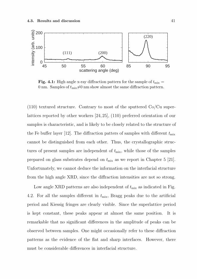
4.3. Results and discussion 41
85 90 950
100
200
45 50 55 60inte
nsity
(ar
b. u
nits
)
scattering angle (deg)
(111) (200)
(220)
Fig. 4.1: High angle x-ray diffraction pattern for the sample of tmix =0 nm. Samples of tmix =0 nm show almost the same diffraction pattern.
(110) textured structure. Contrary to most of the sputtered Co/Cu super-
lattices reported by other workers [24,25], (110) preferred orientation of our
samples is characteristic, and is likely to be closely related to the structure of
the Fe buffer layer [12]. The diffraction patters of samples with different tmix
cannot be distinguished from each other. Thus, the crystallographic struc-
tures of present samples are independent of tmix, while those of the samples
prepared on glass substrates depend on tmix as we report in Chapter 5 [21].
Unfortunately, we cannot deduce the information on the interfacial structure
from the high angle XRD, since the diffraction intensities are not so strong.
Low angle XRD patterns are also independent of tmix as indicated in Fig.
4.2. For all the samples different in tmix, Bragg peaks due to the artificial
period and Kiessig fringes are clearly visible. Since the superlattice period
is kept constant, these peaks appear at almost the same position. It is
remarkable that no significant differences in the amplitude of peaks can be
observed between samples. One might occasionally refer to these diffraction
patterns as the evidence of the flat and sharp interfaces. However, there
must be considerable differences in interfacial structure.

42 Chapter 4. Interfacial structure of Co/Cu superlattices
1x100
1x10²
1x10⁴
1x10⁶
1x10⁸
1x10¹⁰
0 1 2 3 4 5 6 7 8
inte
nsity
(ar
b. u
nits
)
scattering angle (deg)
t mix = 0
t mix = 0.05
t mix = 0.10
t mix = 0.15
t mix = 0.25
Fig. 4.2: Measured low angle x-ray diffraction patterns. The largepeaks at 2θ = 3.1 and 6.2 correspond to the Bragg diffraction for thesuperlattice period. Each pattern is shifted for better understanding.
For semiquantitative interpretation of the interfacial structure, we per-
formed the low angle XRD simulation. To take the low angle corrections into
account, we use a standard optical model by applying a recursive Fresnel
formalism described by Underwood and Barbee [26]. The optical constants
were determined assuming the same lattice constant for Co and Cu evalu-
ated from the high angle XRD. At first, we discuss the effect of the thickness
fluctuation of each layer. Following Fullerton et al. [27], we take the effect of
the thickness fluctuation into account by Monte Calro method. The mean
layer thicknesses of Co and Cu are set at 1.0 and 2.2 nm, respectively, and
the thickness of each layer is selected randomly as its distribution follows
the Gaussian distribution function around the mean thickness. Since the

4.3. Results and discussion 43
calculated reflectivity brings the phase information, the averaged intensity
depends on the averaging procedure. The averaged intensity, excluding the
phase information, is given as [27]
I =1
Nav
Nav∑n=1
|Rn|2, (4.1)
where Rn is the superlattice reflectivity for a superlattices with a particu-
lar random sequence of thickness, while the reflectivity including the phase
information is written as
I =1
Nav
∣∣∣∣∣Nav∑n=1
Rn
∣∣∣∣∣2
. (4.2)
For a more realistic calculation, we must take account of both effects simul-
taneously. In the present case, however, we compare the experiments only
with the calculation of Eqs. (4.1) and (4.2) separately.
Figure 4.3(a) shows the calculated XRD patterns excluding the phase
information for the different thickness fluctuations. In this thesis, the mag-
nitude of the thickness fluctuation is expressed by σf , the standard deviation
of the Gaussian distribution of the thickness. With increasing σf , the in-
tensity of Bragg peaks and the amplitude of Kiessig fringes decrease rapidly.
On the other hand, the decrease with increasing 2θ of the background of the
calculated intensity is almost independent of σf . If we average the reflectivity
of the x-ray including the phase information, the dependence of the calcu-
lated intensity on σf is varied as shown in Fig. 4.3(b). Contrary to the case
excluding the phase information, the background of the calculated intensity
decreases more rapidly with 2θ for the large value of σf .
Obviously, the low angle XRD is very sensitive to the thickness fluctua-
tion. Comparing the calculated XRD patterns with the measured ones, the

44 Chapter 4. Interfacial structure of Co/Cu superlattices
1x10⁻⁸
1x10⁻⁶
1x10⁻⁴
1x10⁻²
1x100
refle
ctiv
ity
1x10⁻¹⁰
1x10⁻⁸
1x10⁻⁶
1x10⁻⁴
1x10⁻²
1x100
0 1 2 3 4 5 6 7 8
refle
ctiv
ity
scattering angle (deg)
(b)
(a)A
B
C
A
B
C
Fig. 4.3: Calculated low angle x-ray diffraction patterns for modelswith thickness fluctuation of σf = 0.05 (line A), 0.10 (line B) and 0.20nm (line C). The x-ray reflectivity is averaged (a) excluding the phaseinformation and (b) including the phase information.
4.3. Results and discussion 45
value of σf for our samples should be less than 0.1 nm and is independent of
tmix. If the codeposited region of tmix ≤ 0.25 nm is regarded as the thickness
fluctuation for the x-ray, the differences in the XRD patterns between our
samples must be observed. This fact suggests that the lateral length of the
thickness fluctuation is much shorter than the coherent length of the x-ray.
When the lateral length of the thickness fluctuation becomes much shorter
than the coherent length of the x-ray, the transition of optical constants from
the Co to the Cu layer will take place over a finite distance. We can take this
effect into account by a sequence of thin layers with average optical constants
approximating the continuous change in the optical constants in the transi-
tion region [26, 27]. Because of the low contrast in the scattering power for
the Co-Cu system, the calculated XRD patterns remain unchanged, if we as-
sume the transition region of the thickness less than 0.25 nm. Consequently,
such a transition region will exist at interfaces of our samples. However,
we cannot deduce the lateral length of roughness and the thickness of the
transition region from the XRD data.
4.3.2 NMR
In contrast to the XRD, the NMR is sensitive to the ASRO. Figure 4.4
shows the frequency spectra of spin-echo intensity of 59Co in the sample of
various tmix. The main peak observed around 210 MHz is attributed to the
signal from the fcc Co atoms with 12 nearest-neighbor Co atoms, while the
resonance frequency is slightly lower than that for bulk Co of 217 MHz. Since
no significant signal was observed on the higher frequency side of the main
peak, the amount of the hcp Co is negligible. There exists a wide distribution

46 Chapter 4. Interfacial structure of Co/Cu superlattices
0.0
0.2
0.4
0.6
0.8
1.0
120 140 160 180 200 220 240
spin
ech
o in
tens
ity (
arb.
uni
ts)
frequency (MHz)
0.0
0.2
0.4
0.6
0.8
1.0
0.0
0.2
0.4
0.6
0.8
1.0
0.0
0.2
0.4
0.6
0.8
1.0(a)
(b)
(c)
(d)
tmix = 0 nm
tmix = 0.10 nm
tmix = 0.15 nm
tmix = 0.25 nm
Fig. 4.4: Frequency spectra of spin-echo intensity of 59Co. The mea-sured data (•) are fitted with five Gaussians (dashed lines). The solidlines indicate the summation of five Gaussians.

4.3. Results and discussion 47
of the hyperfine field in the lower frequency region of the main peak down to
120 MHz. The tail at the frequency lower than that of main peak is due to
the Co atoms near interfaces. Please note that the intensity of tail increases
with tmix. This indicates that the amount of the mixing of Co and Cu atoms
increases with tmix.
For the more quantitative interpretation of the NMR spectra, it is neces-
sary to extract the number of Co atoms with one or more Cu atoms in their
nearest-neighbor shell. The experiment in dilute CoCu alloy indicates that
the resonance frequency shifts with respect to that of bulk by 18 MHz per
Cu atom in nearest-neighbor shell of Co atoms [28]. The similar effect has
been observed for Co/Cu superlattices, although the values of the spacing
between the resonance peaks are not identical with the alloy case due to the
strain [4, 7–12]. Therefore, we analyze the frequency spectra by fitting with
Gaussians. The measured spectra are well fitted with five Gaussians of con-
stant width as indicated by solid lines in Fig. 4.4, where we treat one width
of Gaussians, five peak positions and five peak intensities as free parameters.
The fits are insensitive to the initial parameters and always converge to the
same lines indicated in Fig. 4.4. The errors for the peak positions are less
than 1 MHz, and those for intensities are less than 5 %. The spacing between
the peak positions of each Gaussian is 15±3 MHz. This value is almost in-dependent of the samples and is the same with the value reported for (110)
oriented Co/Cu superlattices [4]. The fits with less than four Gaussians are
poor, while those with more than six Gaussians result in the significant in-
crease in the scatter of the spacing between peaks depending on the samples.
Therefore, we attribute the five Gaussians to the resonance of the Co atoms

48 Chapter 4. Interfacial structure of Co/Cu superlattices
with 12–8 Co atoms in their nearest-neighbor shell.
Assuming the fcc (110) stacking for the superlattices, the probability of
finding the Co atoms, which are surrounded by N nearest-neighbor Co atoms,
in the ith atomic layer is given as [29],
Pi(N) =∑′
Φ(ni−2; 1, pi−2)Φ(ni−1; 4, pi−1)
×Φ(ni; 2, pi)Φ(ni+1; 4, pi+1)Φ(ni+2; 1, pi+2), (4.3)
with the binomial distribution function defined by
Φ(n; z, p) =z!
n!(z − n)!pn(1− p)z−n, (4.4)
where nj is the number of nearest-neighbor Co atoms in the jth atomic layer,
and the summation is taken for all sets satisfying N =∑i+2
j=i−2nj . The value
of pi is the probability of finding a Co atom at a particular nearest-neighbor
site of Co atom, and is given by
pi = xi + αi(1− xi), (4.5)
where xi is the concentration of Co atoms in the ith atomic layer, and αi is
the ASRO parameter. In the case of αi = 0, Co and Cu atoms distribute
randomly, while αi < 0 (αi > 0) corresponds to the ordering (segregation) of
the Co and Cu atoms. Using Eqs. (4.3)–(4.5), we can calculate the number
of Co atoms in one superlattice period with N nearest-neighbor Co atoms as
P (N) =∑
i
xiPi(N), (4.6)
in unit of monolayers (ML), where the summation is taken over one super-
lattice period.

4.3. Results and discussion 49
The frequency spectrum for appropriate chemical composition profile
(CCP) and the ASRO parameters are calculated assuming that the spin-
echo intensity is proportional to P (N) and using the results of Gaussian
fitting for the value of the frequency and the width of 59Co resonance. We
deduced the optimum CCP’s and ASRO parameters to reproduce the mea-
sured frequency spectra by the Davidon-Fletcher-Powell (DFP) method [30].
In the present case, 8 ML of Co exist in a (110) stacked Co layer with a
thickness of 1.0 nm. Thus, we started from the ideal structure consisting of
8 ML of Co, and xi and αi of six atomic layers near interfaces were treated
as parameters.
Resulting CCP’s are shown in Fig. 4.5. The ASRO parameters are almost
zero in all atomic layers for all samples. The calculated frequency spectra
corresponding to CCP’s in Fig. 4.5 coincide with the initial Gaussian fittings
as indicated by solid lines in Fig. 4.4. The shape of the spectrum depends
drastically upon CCP (parameters xi). For example, there are significant
change in the shape of the spectra for the samples of tmix = 0, 0.10 and 0.15
nm [Fig. 4.4(a)–(c)], while the differences in CCP’s for these samples are not
so large [Fig. 4.5(a)–(c)]. This indicates that the NMR has the power to de-
tect the small differences in the CCP. Because of this high sensitivity of NMR
to local composition, CCP’s were determined within the errors indicated by
bars in Fig. 4.5, in spite of the many fitting parameters. For the sample of
tmix = 0 nm, the intermixing extends over 2 atomic layers near interface. The
concentrations of Co in the first and second atomic layers from the interface
are 84 and 97 %, respectively. With increasing tmix, the amount of the in-
termixing increases. On the other hand, the shape of the spectrum is not so

50 Chapter 4. Interfacial structure of Co/Cu superlattices
0.0
0.2
0.4
0.6
0.8
1.0
layers
0.0
0.2
0.4
0.6
0.8
1.0
0.0
0.2
0.4
0.6
0.8
1.0
0.0
0.2
0.4
0.6
0.8
1.0
Co
conc
entr
atio
n
(a)
(b)
(c)
(d)
1 5 10 15 20
tmix = 0
tmix = 0.10
tmix = 0.15
tmix = 0.25
Fig. 4.5: Estimated chemical composition profile in one superlatticeperiod. The histogram shows the estimated Co concentration xi. Thedashed lines indicate the boundaries of the Co layer of 8 ML with idealstructure. The bars indicate the statistical error.

4.4. Conclusion 51
sensitive to the ASRO parameters (αi) in the present case. However, their
values of almost zero are reliable enough to preclude the strong ordering or
segregation of the Co and Cu atoms. Therefore, atoms of Co and Cu are
distributed randomly in the mixed regions.
The results for XRD and NMR are consistent with each other. Since Co
and Cu are randomly mixing at interfaces, the optical constants for x-ray will
change from the Co to Cu layer over a finite distance. On the other hand, the
thickness of the mixing region is uniform in the sample as expected from the
XRD measurements. Therefore, no significant change in the XRD pattern
for the samples of different tmix is observed. These facts confirm that our
samples with different tmix are only different in the distribution of Co atoms
near interfaces, while the superlattice period, the thickness fluctuation and
crystallinity remain unchanged. Consequently, we can control the atomic
roughness of the interfaces in the Co/Cu superlattices by codeposition.
4.4 Conclusion
We have investigated the interfacial structure of Co/Cu superlattices with
artificially mixed interfaces by XRD and 59Co NMR. For the samples of dif-
ferent tmix, no significant change was observed in the XRD patterns. NMR
measurements clarified that Co and Cu atoms distributed randomly in the
interfacial mixed region, and that the CCP of Co was systematically changed
depending on tmix. This indicates clearly that the atomically mixed region in
Co/Cu superlattices cannot be detected by XRD. On the other hand, dynam-
ical simulation for low angle XRD revealed that the XRD was very sensitive
to the thickness fluctuation. Therefore, XRD and NMR are compensative

52 Chapter 4. Interfacial structure of Co/Cu superlattices
with each other.
Using the well-controlled codeposition technique, we can modify only the
CCP in a very thin region near interfaces. The thickness fluctuation, crys-
tallinity and morphology of superlattices are unchanged. Contrary to the
thermal treatment or the sample preparations under various deposition con-
ditions, the interfacial modification by codeposition is a powerful method
to investigate the interfacial phenomena such as GMR. The dependence of
GMR on tmix at room temperature will be reported in Chapter 5 [21], and
its temperature dependence will be reported in Chapter 6 [22].
References
[1] F. Petroff, A. Barthelemy, A. Hamzic, A. Fert, P. Etienne, S. Lequien,
and G. Creuzet, J. Magn. Magn. Mater. 93, 95 (1991).
[2] E. E. Fullerton, D. M. Kelly, J. Guimpel, I. K. Schuller, and Y. Bruynser-
aede, Phys. Rev. Lett. 68, 859 (1992).
[3] M. J. Hall, B. J. Hickey, M. A. Howson, C. Hammond, M. J. Walker,
D. G. Wright, D. Greig, and N. Wiser, J. Phys. Condens. Mater. 4, L495
(1992).
[4] Y. Saito, K. Inomata, A. Goto, and H. Yasuoka, J. Phys. Soc. Jpn. 62,
1450 (1993).
[5] T. C. Huang, J.-P. Nozieres, V. S. Speriosu, H. Lefakis, and B. A. Gur-
ney, Appl. Phys. Lett. 60, 1573 (1992).
References 53
[6] V. S. Speriosu, J. P. Nozieres, B. A. Gurney, B. Dieny, T. C. Huang,
and H. Lefakis, Phys. Rev. B 47, 11579 (1993).
[7] K. L. Dang, P. Veillet, H. He, F. J. Lamelas, C. H. Lee, and R. Clarke,
Phys. Rev. B 41, 12902 (1990).
[8] H. A. M. de Gronckel, K. Kopinga, W. J. M. de Jonge, P. Panissod,
J. P. Schille, and F. J. A. den Broeder, Phys. Rev. B 44, 9100 (1991).
[9] C. Meny, P. Panissod, and R. Loloee, Phys. Rev. B 45, 12269 (1992).
[10] Y. Suzuki, T. Katayama, and H. Yasuoka, J. Magn. Magn. Mater. 104–
107, 1843 (1992).
[11] J. S. Lord, H. Kubo, P. C. Riedi, and H. J. Walker, J. Appl. Phys. 73,
6381 (1993).
[12] M. Suzuki, Y. Taga, A. Goto, and H. Yasuoka, J. Magn. Magn. Mater.
126, 495 (1993).
[13] A. K. Schmid, D. Atlan, H. Itoh, B. Heinrich, T. Ichinokawa, and J.
Kirschner, Phys. Rev. B 48, 2855 (1993).
[14] G. R. Harp, S. S. P. Parkin, R. F. C. Farrow, R. F. Marks, M. F. Toney,
Q. H. Lam, T. A. Rabedeau, and R. J. Savoy, Phys. Rev. B 47, 8721
(1993).
[15] M. T. Kief and W. F. Egelhoff Jr., Phys. Rev. B 47, 10785 (1993).
[16] R. M. Tromp, A. W. Denier van der Gon, and M. C. Reuter, Phys. Rev.
Lett. 68, 2313 (1992).

54 Chapter 4. Interfacial structure of Co/Cu superlattices
[17] J. A. Thornton, Annu. Rev. Mater. Sci. 7, 239 (1977).
[18] Y. Saito, S. Hashimoto, and K. Inomata, Appl. Phys. Lett. 60, 2436
(1992).
[19] R. J. Highmore, W. C. Shih, R. E. Somekh, and J. E. Evetts, J. Magn.
Magn. Mater. 116, 249 (1992).
[20] K. Takanashi, Y. Obi, Y. Mitani, and H. Fujimori, J. Phys. Soc. Jpn.
61, 1169 (1992).
[21] M. Suzuki and Y. Taga, J. Appl. Phys. 74, 4660 (1993).
[22] M. Suzuki and Y. Taga, Phys. Rev. B 52, 361 (1995).
[23] H. Yasuoka, inMetallic Superlattices, edited by T. Shinjo and T. Takada
(Elsevier, Amsterdam, 1987), p. 159.
[24] S. S. P. Parkin, R. Bhadra, and K. P. Roche, Phys. Rev. Lett. 66, 2152
(1991).
[25] D. H. Mosca, F. Petroff, A. Fert, P. A. Schroeder, W. P. Pratt Jr., and
R. Laloee, J. Magn. Magn. Mater. 94, L1 (1991).
[26] J. H. Underwood and T. W. Barbee Jr., Appl. Opt. 20, 3027 (1981).
[27] E. E. Fullerton, I. K. Schuller, H. Vanderstraeten, and Y. Bruynseraede,
Phys. Rev. B 45, 9292 (1992).
[28] S. Nasu, H. Yasuoka, Y. Nakamura, and Y. Murakami, Acta Metall. 22,
1057 (1974).

References 55
[29] N. Hamada, K. Terakura, K. Takanashi, and H. Yasuoka, J. Phys. F 15,
835 (1985).
[30] R. Fletcher and M. J. Powell, The Computer Journal 6, 163 (1963).

Chapter 5
GMR in Co/Cu superlatticeswith mixed interfaces I∼ Effect of interfacial roughness on
GMR and AF coupling
Abstract
Magnetoresistance, antiferromagnetic coupling and crystallographicorientation of Co/Cu superlattices with intentionally mixed interfaceshave been studied as a function of the thickness of the mixed region.The antiferromagnetic coupling is weakened, and spin-independentscattering of free electrons is enhanced with increasing thickness ofthe mixed region, although the morphology and superlattice periodremain unchanged. Saturation magnetoresistance is reduced from 27% to 4 % as the result of formation of 0.15 nm mixed region at in-terfaces. Giant magnetoresistance and antiferromagnetic coupling ofCo/Cu superlattices are governed by the events in thin region at in-terfaces less than 1 monolayer.
57
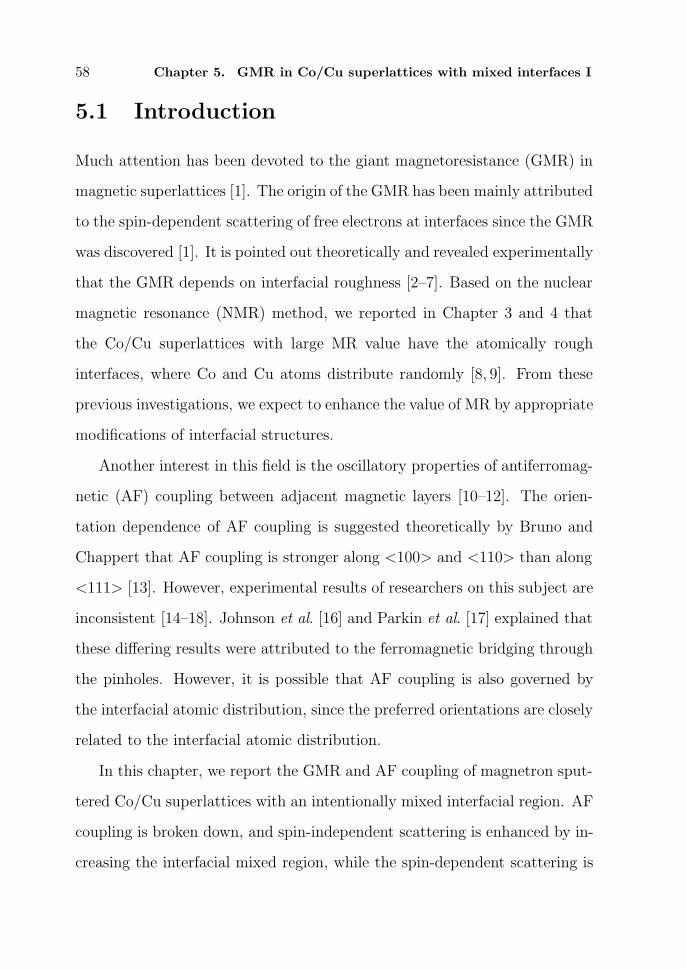
58 Chapter 5. GMR in Co/Cu superlattices with mixed interfaces I
5.1 Introduction
Much attention has been devoted to the giant magnetoresistance (GMR) in
magnetic superlattices [1]. The origin of the GMR has been mainly attributed
to the spin-dependent scattering of free electrons at interfaces since the GMR
was discovered [1]. It is pointed out theoretically and revealed experimentally
that the GMR depends on interfacial roughness [2–7]. Based on the nuclear
magnetic resonance (NMR) method, we reported in Chapter 3 and 4 that
the Co/Cu superlattices with large MR value have the atomically rough
interfaces, where Co and Cu atoms distribute randomly [8, 9]. From these
previous investigations, we expect to enhance the value of MR by appropriate
modifications of interfacial structures.
Another interest in this field is the oscillatory properties of antiferromag-
netic (AF) coupling between adjacent magnetic layers [10–12]. The orien-
tation dependence of AF coupling is suggested theoretically by Bruno and
Chappert that AF coupling is stronger along <100> and <110> than along
<111> [13]. However, experimental results of researchers on this subject are
inconsistent [14–18]. Johnson et al. [16] and Parkin et al. [17] explained that
these differing results were attributed to the ferromagnetic bridging through
the pinholes. However, it is possible that AF coupling is also governed by
the interfacial atomic distribution, since the preferred orientations are closely
related to the interfacial atomic distribution.
In this chapter, we report the GMR and AF coupling of magnetron sput-
tered Co/Cu superlattices with an intentionally mixed interfacial region. AF
coupling is broken down, and spin-independent scattering is enhanced by in-
creasing the interfacial mixed region, while the spin-dependent scattering is

5.2. Experiment 59
almost constant.
5.2 Experiment
The Co/Cu superlattices with artificially mixed interfaces were prepared in
the same manner as described in Chapter 4, except for the substrates. The
samples discussed in this chapter were deposited on a glass substrate. The
amount of Co and Cu deposited in each Co/Cu bilayer was kept constant at
1.0 and 2.0 nm for pure Co and Cu. This combination of thickness of Co and
Cu corresponds to the second peak of oscillatory properties of GMR and AF
coupling as a function of Cu layer thickness [10–12]. Since the second peak
is broader than the first peak around the Cu layer thickness of 1.0 nm (see
Fig. 3.1), the influence of the variation of Cu layer thickness on the GMR
and AF coupling is considered to be small.
The MR was measured at room temperature, using a conventional four-
point geometry. The current is in the plane of the film with the magnetic
field in-plane and orthogonal to the current direction. The in-plane mag-
netization of the samples was also measured with SQUID magnetometer at
room temperature. The structures of samples were characterized by x-ray
diffraction.
5.3 Results and discussion
Comparison of the magnetoresistance (MR) and magnetization curves be-
tween the samples with and without mixed interfaces is shown in Fig. 5.1.
The MR ratio at magnetic field H is defined as [ρ(H)− ρs]/ρs, where ρ(H)
is the resistivity at the field of H, and ρs is the saturation resistivity. In
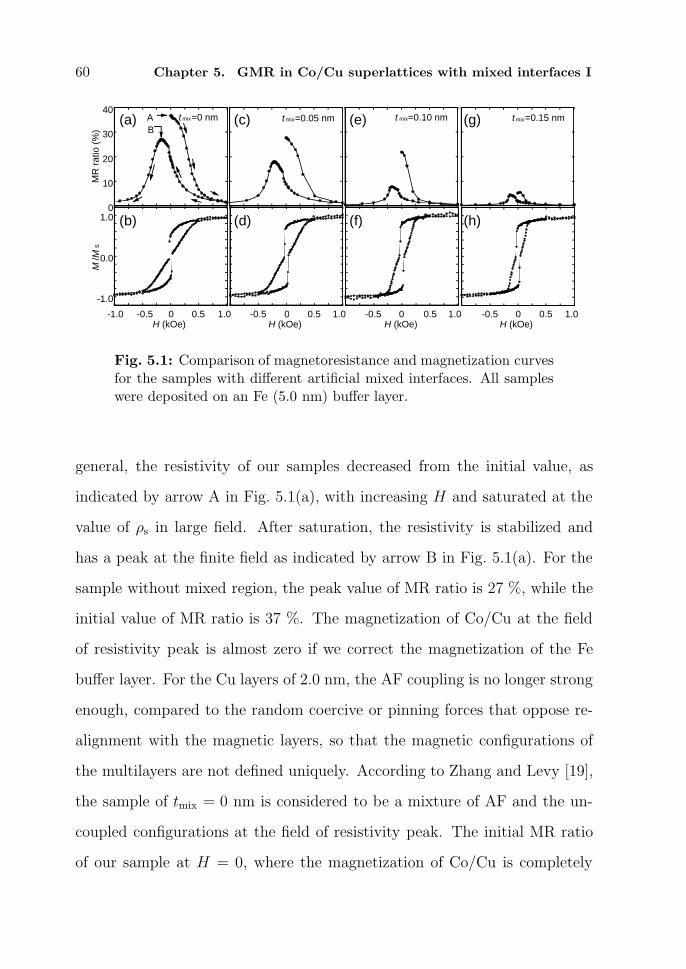
60 Chapter 5. GMR in Co/Cu superlattices with mixed interfaces I
0
10
20
30
40
MR
rat
io (
%)
-1.0
0.0
1.0
M /M
s
1.00.50-0.5H (kOe)
t =0.05 nm
1.00.50-0.5H (kOe)
t =0.10 nm
1.00.50-0.5H (kOe)
t =0.15 nm
1.00.50-0.5-1.0H (kOe)
t =0 nm(a)
(b)
(c)
(d)
(e)
(f)
(g)
(h)
AB
mix mix mix mix
Fig. 5.1: Comparison of magnetoresistance and magnetization curvesfor the samples with different artificial mixed interfaces. All sampleswere deposited on an Fe (5.0 nm) buffer layer.
general, the resistivity of our samples decreased from the initial value, as
indicated by arrow A in Fig. 5.1(a), with increasing H and saturated at the
value of ρs in large field. After saturation, the resistivity is stabilized and
has a peak at the finite field as indicated by arrow B in Fig. 5.1(a). For the
sample without mixed region, the peak value of MR ratio is 27 %, while the
initial value of MR ratio is 37 %. The magnetization of Co/Cu at the field
of resistivity peak is almost zero if we correct the magnetization of the Fe
buffer layer. For the Cu layers of 2.0 nm, the AF coupling is no longer strong
enough, compared to the random coercive or pinning forces that oppose re-
alignment with the magnetic layers, so that the magnetic configurations of
the multilayers are not defined uniquely. According to Zhang and Levy [19],
the sample of tmix = 0 nm is considered to be a mixture of AF and the un-
coupled configurations at the field of resistivity peak. The initial MR ratio
of our sample at H = 0, where the magnetization of Co/Cu is completely

5.3. Results and discussion 61
zero, was larger than the peak value of the MR ratio. These indicate that
the Co/Cu superlattices are more completely AF coupled at the initial stage.
The value of MR ratio and saturation field Hs decrease with increasing
tmix. Figure 5.2 shows the variation ofHs, ρs, ∆ρ and∆ρ0 with tmix, where ∆ρ
is the difference between ρs and peak resistivity ρp, and ∆ρ0 is the difference
between ρs and initial resistivity ρ0. Clearly, the Hs decreases with increasing
tmix to 0.15 nm, which is comparable with 1 ML. The decrease of Hs cannot
be attributed to the increase of ferromagnetic bridging of Co layers through
the pinholes due to the change in topological roughness. Figure 5.3 shows
the low angle x-ray diffraction patterns of samples deposited on the Fe buffer
layer of 5.0 nm. Since the amount of Co and Cu deposited in each Co/Cu
bilayer was kept constant, there is not significant change in the position of
the peak due to the artificial period. Moreover, the intensity and width of
these peaks are also almost identical for all samples. As described in Chapter
4, no significant change in topological roughness can be found [9]. Therefore,
the decrease of Hs is attributed to the weakening of AF coupling between
adjacent Co layers.
It is remarkable that the interfacial mixing thinner than 1 ML breaks the
interlayer AF coupling. This variation in AF coupling cannot be explained
by the orientation dependence of AF coupling. Figure 5.4 shows the high
angle x-ray diffraction patterns for samples with different tmix. The sample
without the mixed region shows the weak (111) and (200) diffraction peaks.
For the sample with the mixed region of tmix = 0.05 and 0.10 nm, the (111)
diffraction peak disappears while the intensity of (220) peak increases. When
the interfacial region is mixed by a 0.15 nm thickness, the diffraction pat-

62 Chapter 5. GMR in Co/Cu superlattices with mixed interfaces I
0
0.1
0.2
0.3
0.4
0.5
0.6
10
12
14
16
18
0
2
4
6
0 0.05 0.1 0.15
Hs
(kO
e)ρ s
(µΩ
cm)
∆ρ(µ
Ωcm
)ρs
∆ρ
∆ρ0
(a)
(b)
Fig. 5.2: The variation of the saturation field (a), saturation resistiv-ity, and magnetoresistivity (b) depending on the thickness of mixedregion for samples deposited on Fe (5.0 nm) buffer layer.

5.3. Results and discussion 63
2 3 4 52θ (deg)
diffr
actio
n in
tens
ity t =0 nmmix
t =0.05 nmmix
t =0.10 nmmix
t =0.15 nmmix
Fig. 5.3: Low angle x-ray diffraction patterns for the samples withartificial mixed interfaces of different thickness. All samples were de-posited on an Fe (5.0 nm) buffer layer.

64 Chapter 5. GMR in Co/Cu superlattices with mixed interfaces I
50 55 6045 9085 95
diffr
actio
n in
tens
ity
2θ (deg)
(111)
(200)
(220)
t =0 nmmix
t =0.05 nmmix
t =0.10 nmmix
t =0.15 nmmix
Fig. 5.4: High angle x-ray diffraction patterns for samples with artifi-cial mixed interfaces of different thickness. All samples were depositedon an Fe (5.0 nm) buffer layer.

5.3. Results and discussion 65
tern is similar to that of the sample without the mixed region. Therefore,
it seems that there is no correlation between the preferred orientation and
AF coupling. It is surprising that the addition of a very thin mixed region
less than 1 ML changes the crystallinity of Co/Cu superlattices. This de-
pendence of the preferred orientation on tmix is a characteristic feature for
the samples deposited on the glass substrate, and cannot be found for the
samples deposited on the surface-oxidized Si substrate as shown in Chapter
4.
In previous studies, it was reported that strong AF coupling and larger
MR were observed for magnetron sputtered Co/Cu and NiFe/Co superlat-
tices with a weak tendency to (111) textured structure [8,14,18]. Egelhoff and
Kief indicated that (111) stacked single crystal Co/Cu grown by molecular
beam epitaxy (MBE) did not show the AF coupling [15]. Recently, Johnson
et al. [16] and Parkin et al. [17], however, observed strong AF coupling for
MBE grown (111) stacked and magnetron sputtered (111) textured Co/Cu
superlattices. The complication between these investigations may be due
to not only the ferromagnetic bridging, but also the existence of very thin
interfacial mixing.
The weakening of AF coupling is one of the reasons why the MR ra-
tio decreases with increasing tmix. The other is the increase of saturation
resistivity ρs, as shown in Fig. 5.2(b). The increase of ρs is attributed to
the increase of spin-independent scattering. Therefore, the interfacial mixed
region is considered to play a role in spin-independent scattering center.
We can expect that the highly disordered interfacial structure enhances
the spin-dependent scattering. Oguri et al. suggest in their theoretical inves-

66 Chapter 5. GMR in Co/Cu superlattices with mixed interfaces I
tigation that spin-dependent scattering is enhanced by increasing the degree
of randomness of the interfacial atomic distribution [7]. In fact, Co and Cu
atoms distribute randomly in the interfacial mixed region as described in the
previous chapter. However, we can observe no significant enhancement of the
spin-dependent scattering, since the ∆ρ0 is almost constant up to tmix = 0.10
nm. The dependence of ∆ρ0 on tmix will be the results of not only the vari-
ation of the spin-dependent interfacial scattering but also the variation of
the strength of the AF coupling. Thus, we can only conclude here that the
interfacial scattering in Co/Cu superlattices is less spin-dependent than that
in Fe/Cr superlattices in which the MR ratio increases with increasing in-
terfacial roughness [2, 20]. Detailed analysis of the spin-dependence of the
interfacial scattering will be discussed in the next chapter.
5.4 Conclusion
We have prepared Co/Cu superlattices with mixed region less than 1 ML on
the glass substrates and have studied MR and AF coupling. The decrease of
the MR ratio with increasing thickness of the mixed region can be attributed
to the weakening of AF coupling and enhancement of spin-independent scat-
tering of free electrons.
The interfacial mixed region discussed here is so thin that similar mix-
ing can be formed in the deposition process or annealing after deposition.
For example, many energetic ions and neutral particles bombard the sam-
ple surface during deposition by sputtering. The energy of these particles is
sometimes great enough to cause interfacial mixing. Mixing by thermal dif-
fusion also occurs, if the temperature of the samples rises during deposition.

References 67
We consider that the existence of the mixed regions complicates studies on
AF coupling and GMR of the magnetic superlattice.
In the next chapter, we discuss the detailed properties of the interfacial
scattering based on the temperature and magnetization dependence of the
GMR.
References
[1] M. N. Baibich, J. M. Broto, A. Fert, F. Nguyen Van Dau, F. Petroff, P.
Etienne, G. Creuzet, A. Friederich, and J. Chazelas, Phys. Rev. Lett.
61, 2472 (1988).
[2] E. E. Fullerton, D. M. Kelly, J. Guimpel, I. K. Schuller, and Y. Bruynser-
aede, Phys. Rev. Lett. 68, 859 (1992).
[3] Y. Saito, K. Inomata, A. Goto, and H. Yasuoka, J. Phys. Soc. Jpn. 62,
1450 (1993).
[4] H. Hasegawa, Phys. Rev. B 42, 2368 (1990).
[5] P. M. Levy, K. Ounadjela, S. Zhang, Y. Wang, C. B. Sommers, and A.
Fert, J. Appl. Phys. 67, 5914 (1990).
[6] Y. Wang, P. M. Levy, and L. L. Fry, Phys. Rev. Lett. 65, 2732 (1990).
[7] A. Oguri, Y. Asano, and S. Maekawa, J. Phys. Soc. Jpn. 61, 2652 (1992).
[8] M. Suzuki, Y. Taga, A. Goto, and H. Yasuoka, J. Magn. Magn. Mater.
126, 495 (1993).
68 Chapter 5. GMR in Co/Cu superlattices with mixed interfaces I
[9] M. Suzuki, Y. Taga, A. Goto, and H. Yasuoka, Phys. Rev. B 50, 18580
(1994).
[10] S. S. P. Parkin, R. Bhadra, and K. P. Roche, Phys. Rev. Lett. 66, 2152
(1991).
[11] D. H. Mosca, F. Petroff, A. Fert, P. A. Schroeder, W. P. Pratt Jr., and
R. Laloee, J. Magn. Magn. Mater. 94, L1 (1991).
[12] S. S. P. Parkin, Phys. Rev. Lett. 67, 3598 (1991).
[13] P. Bruno and C. Chappert, Phys. Rev. Lett. 67, 1602 (1991).
[14] M. E. Tomlinson, R. J. Pollard, D. J. Lord, and P. J. Grundy, J. Magn.
Magn. Mater. 111, 79 (1992).
[15] W. F. Egelhoff Jr. and M. T. Kief, Phys. Rev. B 45, 7795 (1992).
[16] M. T. Johnson, R. Coehoorn, J. J. de Vries, N. W. E. McGee, J. aan de
Stegge, and P. J. H. Bloemen, Phys. Rev. Lett. 69, 969 (1992).
[17] S. S. P. Parkin, R. F. Marks, R. F. C. Farrow, G. R. Harp, Q. H. Lam,
and R. J. Savoy, Phys. Rev. B 46, 9262 (1992).
[18] R. Nakatani, T. Dei, and Y. Sugita, Jpn. J. Appl. Phys. 31, L1417
(1992).
[19] S. Zhang and P. M. Levy, Phys. Rev. B 47, 6776 (1993).
[20] F. Petroff, A. Barthelemy, A. Hamzic, A. Fert, P. Etienne, S. Lequien,
and G. Creuzet, J. Magn. Magn. Mater. 93, 95 (1991).

Chapter 6
GMR in Co/Cu superlatticeswith mixed interfaces II∼ Mechanism of spin-dependent
scattering
Abstract
We have measured both the magnetization and the temperaturedependence of the giant magnetoresistance (GMR) in Co/Cu super-lattices with different interfacial roughness. The magnetization de-pendence of the magnetoresistance (MR) has precluded the existenceof a strong spin dependence in the potential not only for the bulkbut also for the interfacial scattering. The temperature dependenceof the GMR is hardly influenced by the interfacial roughness, whilethe residual resistivity changes significantly. The residual MR ratiodecreases with increasing interfacial roughness. This reveals that thespin-dependent s–d scattering in the bulk is crucial for the GMR inCo/Cu superlattices. The interfacial roughness mainly contributes tothe residual resistivity, and the spin dependence in the scattering atinterfaces is weaker than that in the bulk.
69

70 Chapter 6. GMR in Co/Cu superlattices with mixed interfaces II
6.1 Introduction
A great number of attempts have been made to clarify the origin of the giant
magnetoresistance (GMR) observed in various magnetic multilayers [1–3].
Most of them have focused on the spin-dependent scattering of conduc-
tion electrons. Some theoretical studies attribute the GMR to the spin-
dependent potential at interfaces [4–6]. In these theories, interfacial rough-
ness is required as the scattering center. The strong spin-dependent scat-
tering also comes from the spin-split density-of-states (SSDOS) for majority-
and minority-spin d bands in the magnetic layers and occurs both in the bulk
and at the interfaces [7, 8].
On the other hand, many experimental studies deal with the correlation
between the GMR and the interfacial roughness to understand the role of
interfaces [9–14]. For Fe/Cr superlattices [9, 10], the enhancement of both
the magnitude and temperature dependence of the GMR due to interfacial
roughness has been reported, so that the origin of the GMR in Fe/Cr is
attributed to the interfacial scattering [5]. However, for transition metal/Cu
superlattices, no one has reported that the interfacial roughness enhances
the GMR [11–14]. Nevertheless, the importance of interfacial scattering has
been pointed out indirectly in studies on the layer thickness dependence
of the GMR [15, 16]. The mechanism of the GMR in transition metal/Cu
superlattices still remains unclear.
This lack of understanding lies in the difficulty of quantitatively under-
standing the relationship between the interfacial structure and the transport
properties since the interfacial structure is difficult to control and analyze.
As reported in Chapter 4 [17], we succeeded in preparing Co/Cu superlat-

6.2. Experiment 71
tices with well-controlled interfacial roughness. In these samples, only the
atomic interfacial roughness has been modified, while the morphology and
the crystallinity remain unchanged. This enables us to study the effect of in-
terfacial roughness on the magnetization and the temperature dependence of
the GMR. In this chapter, our experimental data are analyzed by the SSDOS
model based on the theory proposed by Xing et al. [7,8]. The results suggest
that the GMR in Co/Cu superlattices mainly comes from the spin-dependent
s–d scattering in the Co layers.
6.2 Experiment
Since the details of the sample preparation and characterization have been
reported in Chapter 2 and 4 [17], we only briefly describe them here. The
Co/Cu superlattices with artificially mixed interfaces were deposited on an
Fe buffer layer of a thickness of 5.0 nm prepared on a surface-oxidized Si sub-
strate in the same manner as described in Chapter 4. The number of Co/Cu
bilayers was 16, and the thicknesses of Co and Cu in a period were kept
constant at 1.0 and 2.2 nm, respectively. The nominal structure of a sam-
ple was as follows: substrate/Fe(5.0)/Cu(2.2−tmix/2)/CoCu(tmix)/[Co(1.0−tmix)/CoCu(tmix)/Cu(2.2−tmix)/CoCu(tmix)]15/Co(1.0−tmix)/Cu(2.2−tmix/2),
where tmix is the nominal thickness of the codeposited regions, and the values
in the parentheses are the thickness of respective layers in unit of nm. The
value of tmix was varied between 0 and 0.25 nm. The thickness fluctuation
of each layer, characterized using x-ray diffraction, was less than 0.1 nm for
all samples independently of tmix. On the other hand,59Co NMR revealed
that Co and Cu atoms were atomically mixed at the interfaces and that the

72 Chapter 6. GMR in Co/Cu superlattices with mixed interfaces II
amount of interfacial mixing increased according to the value of tmix.
The in-plane magnetoresistance (MR) was measured with a standard
dc four-terminal geometry as a function of the temperature in the range
2≤T≤300 K. The dimension of the samples for the measurement was 2×15mm2, and the current used was 1 mA. This confirms that the resolution of the
measured resistance is better than 10−3 Ω. In order to minimize the error due
to the thermoelectric power in the measurement circuit, we averaged two se-
quential measurements with different polarities of the current. This sequence
was repeated more than 50 times keeping the temperature constant for 10
min, and the collected data were averaged. The standard deviation for the
data was smaller than the order of 10−4 Ω. The resistance-to-resistivity con-
version was performed by scaling using the resistivity measured with samples
at 300 K large enough to obtain an accuracy of 10−2 µΩcm. As a result, for
one sample, the accuracy of the absolute value of resistivity was 10−2 µΩcm,
while the resolution was better than 10−3 µΩcm. Furthermore, the scatter-
ing of the data due to the sample reproducibility, which was obtained from
measurements for five series of samples, was within ±1 µΩcm.
The magnetization was also measured with a superconducting quantum
interface device (SQUID) magnetometer.
6.3 Results and discussion
6.3.1 Relationship between GMR and magnetization
Figure 6.1 shows the MR curves measured at 5 K for one of the series of the
samples with different tmix. The MR ratio is defined as (ρ− ρs)/ρs, where ρ
is the resistivity in an arbitrary field and ρs is the saturation resistivity. In
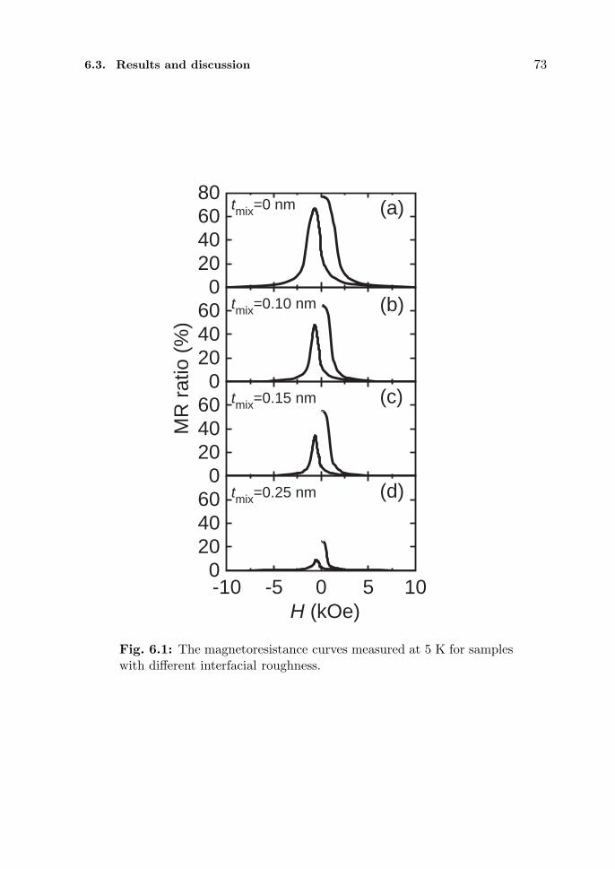
6.3. Results and discussion 73
020406080
0204060
0204060
0204060
-10 -5 0 5 10
MR
rat
io (
%)
(a)
(b)
(c)
(d)
H (kOe)
tmix=0.10 nm
tmix=0 nm
tmix=0.15 nm
tmix=0.25 nm
Fig. 6.1: The magnetoresistance curves measured at 5 K for sampleswith different interfacial roughness.
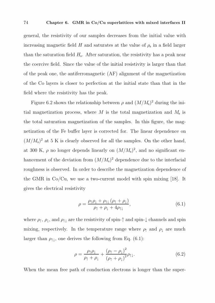
74 Chapter 6. GMR in Co/Cu superlattices with mixed interfaces II
general, the resistivity of our samples decreases from the initial value with
increasing magnetic field H and saturates at the value of ρs in a field larger
than the saturation field Hs. After saturation, the resistivity has a peak near
the coercive field. Since the value of the initial resistivity is larger than that
of the peak one, the antiferromagnetic (AF) alignment of the magnetization
of the Co layers is closer to perfection at the initial state than that in the
field where the resistivity has the peak.
Figure 6.2 shows the relationship between ρ and (M/Ms)2 during the ini-
tial magnetization process, where M is the total magnetization and Ms is
the total saturation magnetization of the samples. In this figure, the mag-
netization of the Fe buffer layer is corrected for. The linear dependence on
(M/Ms)2 at 5 K is clearly observed for all the samples. On the other hand,
at 300 K, ρ no longer depends linearly on (M/Ms)2, and no significant en-
hancement of the deviation from (M/Ms)2 dependence due to the interfacial
roughness is observed. In order to describe the magnetization dependence of
the GMR in Co/Cu, we use a two-current model with spin mixing [18]. It
gives the electrical resistivity
ρ =ρ↑ρ↓ + ρ↑↓ (ρ↑ + ρ↓)
ρ↑ + ρ↓ + 4ρ↑↓, (6.1)
where ρ↑, ρ↓, and ρ↑↓ are the resistivity of spin-↑ and spin-↓ channels and spinmixing, respectively. In the temperature range where ρ↑ and ρ↓ are much
larger than ρ↑↓, one derives the following from Eq. (6.1):
ρ =ρ↑ρ↓
ρ↑ + ρ↓+(ρ↑ − ρ↓)
2
(ρ↑ + ρ↓)2ρ↑↓. (6.2)
When the mean free path of conduction electrons is longer than the super-
6.3. Results and discussion 75
resi
stiv
ity(µ
Ωcm
)
8
10
12
14
16
18
205 K
(a)
M / Ms
2
resi
stiv
ity(µ
Ωcm
)
12
14
16
18
20
22
24
0 0.5 1.0
300 K
(b)
Fig. 6.2: The relationship between ρ(m) and (M/Ms)2 during theinitial magnetization process measured at 5 K (a) and 300 K (b) forthe samples of tmix = 0 (•), 0.10 (), 0.15 (), and 0.25 () nm.The magnetization of the Fe buffer layer is corrected for. The linesindicate a guide for the eyes.

76 Chapter 6. GMR in Co/Cu superlattices with mixed interfaces II
lattice period, ρ↑ and ρ↓ are given as [7, 8, 19]
ρ↑(m) =η
2
2(1− η)
ηρN + ρ+ + ρ−
+η
2(ρ+ − ρ−)m, (6.3)
ρ↓(m) =η
2
2(1− η)
ηρN + ρ+ + ρ−
−η
2(ρ+ − ρ−)m, (6.4)
where ρN is the resistivity of the nonmagnetic layer, ρ+ and ρ− are the re-
sistivities of the magnetic layer for majority- and minority-spin electrons,
respectively, and η is the thickness fraction of the magnetic layer in one
superlattice period. The value of m is determined by the geometric con-
figuration of the magnetization of the magnetic layers. For completely AF
coupled superlattices, m = M/Ms [7, 8, 20]. We write here the resistivities
for both spin channels as ρ↑(m) and ρ↓(m) to express the dependence on m
explicitly. Substituting Eqs. (6.3) and (6.4) into Eq. (6.2), the resistivity in
a field is given by
ρ(m) = ρAF −η (ρ+ − ρ−)
4
2(1− ρ↑↓(m)
ρAF
)m2
ρAF, (6.5)
where ρAF is the resistivity when the magnetization of the magnetic layers is
perfectly AF aligned and is written as
ρAF ≡ ρ(m = 0) =η
4
2 (1− η)
ηρN + ρ+ + ρ−
. (6.6)
Here, we allow the spin mixing to depend on m. As can be seen from Eq.
(6.5), ρ(m) changes linearly with m2, when ρ↑↓(m) is negligible. If the AF
alignment of the magnetization of Co is perfect, ρ(m) changes linearly with

6.3. Results and discussion 77
(M/Ms)2 [20]. Therefore the magnetic configuration of our samples is very
close to the perfect AF alignment at the initial state (see Fig. 6.2). Never-
theless, the magnitude of the saturation MR ratio decreases with increasing
tmix as shown in Fig. 6.1. This indicates that the spin dependence in the
scattering of conduction electrons from interfacial roughness is weaker than
that in the Co layers.
In addition to the imperfect AF alignment, the spin mixing [7, 8] and
Hasegawa’s valve effect [21,22] cause deviation from the (M/Ms)2 dependence
of ρ(m). Thus the existence of significant spin mixing and the valve effect
are precluded for our samples at 5 K. Xing et al. [7, 8] indicated that the
spin mixing at low temperature comes from the spin-dependent diagonal
matrix elements of the potential for the scattering of electrons with each spin
direction. They showed that it made the resistivity larger than the (M/Ms)2
dependence in any field of 0 < H < Hs. The present result suggests that
the spin dependence in the scattering potential for both bulk and interfacial
scattering is not very strong. Therefore the GMR in Co/Cu arises from
the spin-dependent s–d scattering rate due to the different density of states
(DOS) for majority- and minority-spin d bands in the magnetic layer.
The deviation from (M/Ms)2 dependence at 300 K is likely to be due to
the spin mixing. Since ρ(m) deviates downwards from the linear dependence
on (M/Ms)2 in a field of 0 < H < Hs, this does not come from the spin
dependence of the scattering potential. We believe that the spin mixing at
300 K is due to thermal excitation of magnons and we have to take account
of not only the diagonal but also the off-diagonal matrix elements. However,
the interfacial roughness does not play an important role in the spin mixing,
78 Chapter 6. GMR in Co/Cu superlattices with mixed interfaces II
since no significant difference in the magnitude of the deviation from the
(M/Ms)2 dependence between the samples with different tmix is observed.
6.3.2 Temperature dependence of GMR
We examined the effect of the interfacial roughness on the temperature de-
pendence of the GMR with our attention on the initial resistivity ρ0 and the
saturation resistivity ρs. As mentioned above, the samples in the initial state
have almost perfect AF alignment. Furthermore, we can keep the magnetic
configuration constant during the measurements of temperature dependence
of ρ0 and ρs. Figure 6.3 shows the temperature dependence of ρ0 and ρs to-
gether with that of ∆ρ0 = ρ0 − ρs for the samples of various tmix. With
increasing temperature, both ρ0 and ρs increase due to electron-phonon,
electron-magnon, or other scattering processes. The residual resistivity of
ρs increases with increasing tmix due to the increase in interfacial scatter-
ing, though the difference in the temperature coefficient is small. Since the
temperature coefficient of ρs is larger than that of ρ0, ∆ρ0 decreases with
increasing temperature. The deviations of ρ0 and ρs from their values at 2
K are shown in Fig. 6.4. A minimum in ρ0 is found at around 15 K for the
samples of tmix≤0.15 nm, while ρs increases monotonically with increasing
temperature. As indicated in Ref. [23], the minimum in ρ0 is the character-
istic feature for AF coupled Co/Cu superlattices. However, the minimum is
not found for the sample of tmix = 0.25 nm.
Since the spin mixing does not contribute to ρ0 explicitly [see Eq. (6.5)],
the spin mixing in ρs is one of the processes reducing the value of ∆ρ0 with
increasing temperature. However, the minimum in ρ0 [Fig. 6.4(a)] indicates

6.3. Results and discussion 79
101214161820
14161820222426
2
4
6
8
0 50 100 150 200 250 300temperature (K)
ρ 0(µ
Ωcm
)ρ s
(µΩ
cm)
∆ρ0
(µΩ
cm)
(a)
(b)
(c)
Fig. 6.3: Temperature dependence of (a) ρ0, (b) ρs, and (c) ∆ρ0 forthe samples of tmix = 0 (•), 0.10 (), 0.15 (), and 0.25 () nm. Notethat the vertical scale for (c) is different from the others. The linesindicate a guide for the eyes.
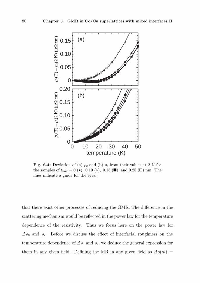
80 Chapter 6. GMR in Co/Cu superlattices with mixed interfaces II
0
0.05
0.10
0.15 (a)
ρ 0(T
)–
ρ 0(2
K)
(µΩ
cm)
0
0.05
0.10
0.15
0.20
0 10 20 30 40 50temperature (K)
ρ s(T
)–
ρ s(2
K)
(µΩ
cm)
(b)
Fig. 6.4: Deviation of (a) ρ0 and (b) ρs from their values at 2 K forthe samples of tmix = 0 (•), 0.10 (), 0.15 (), and 0.25 () nm. Thelines indicate a guide for the eyes.
that there exist other processes of reducing the GMR. The difference in the
scattering mechanism would be reflected in the power law for the temperature
dependence of the resistivity. Thus we focus here on the power law for
∆ρ0 and ρs. Before we discuss the effect of interfacial roughness on the
temperature dependence of ∆ρ0 and ρs, we deduce the general expression for
them in any given field. Defining the MR in any given field as ∆ρ(m) ≡
6.3. Results and discussion 81
ρ(m)− ρ(m = 1) = ρ(m)− ρs, Eq. (6.4) is written as
∆ρ(m) =
η (ρ+ − ρ−)
4
21
ρAF
1−m2 − ρ↑↓(m = 1)−m2ρ↑↓(m)
ρAF
. (6.7)
In the temperature range where ρ↑↓ρAF,
∆ρ(m) =(1−m2
)(ρAF − ρs) . (6.8)
Equation (6.8) indicates that ∆ρ(m) is proportional to ρAF − ρs, whenever
the geometric factor m is kept constant. Note that this is correct even in
the case that the AF alignment of magnetization of Co is imperfect (nonzero
m). In the high temperature region, care must be taken to interpret the
temperature dependence of ∆ρ(m), since the spin mixing comes into the
expression for ∆ρ(m).
Figures 6.5 and 6.6 show double logarithmic plots of ρs(T )− ρs(2 K) and
∆ρ0(2 K)−∆ρ0(T ). At temperatures lower than 100 K, ρs closely approx-
imates a T 2 power law. The temperature dependence of ρs changes to T n
(n = 1−1.5) over 100 K. This temperature dependence cannot be attributedonly to the spin mixing, since spin mixing obeys a T3/2 power law at low tem-
peratures and a T 2 power law at high temperatures [18]. The spin mixing
found in Fig. 6.2(b) will be superimposed on the large temperature depen-
dence due to other excitations. The electron-electron or electron-magnon
scattering is a possible mechanism to explain the T2 dependence, although
details of the process have not been clarified. On the other hand, ∆ρ0 changes
linearly with T 3/2 over the whole measurement temperature range. As can
be seen from Eqs. (6.6) and (6.7), decrease in ∆ρ0 is caused by a decrease
in |ρ+ − ρ−| and increase in ρAF. Since 1/ρAF does not simply depend on

82 Chapter 6. GMR in Co/Cu superlattices with mixed interfaces II
1x10⁻³
1x10⁻²
1x10⁻¹
1x100
1x101
1x10²
1x10³
1x10⁴
4 10 100 400temperature (K)
T 2ρ s
(T)
–ρ s
(2K
)(µ
Ωcm
)
Fig. 6.5: Double logarithmic plot of ρs(T ) − ρs(2 K) versus tem-perature for the samples of tmix = 0 (•), 0.10 (), 0.15 (), and0.25 () nm. For the better understanding, the data for the sampleof tmix =0.10, 0.15, and 0.25 nm are multiplied by 10, 102,and 103,respectively.
T 3/2, the term |ρ+ − ρ−| plays an important role in the temperature depen-dence of ∆ρ0. Since |ρ+ − ρ−| reflects the difference in population betweenthe majority- and minority-spin d bands in Co, it should be closely related
to the spontaneous magnetization. Saito et al. [23] indicated that ∆ρ0 and
the spontaneous magnetization showed a similar temperature dependence.
In fact, the spontaneous magnetization of our samples also shows the T3/2
dependence. However, the relationship between them is more complicated
than a simple linear relation.
As shown in Figs. 6.5 and 6.6, the power laws for ∆ρ0 and ρs are inde-

6.3. Results and discussion 83
1x10⁻³
1x10⁻²
1x10⁻¹
1x100
1x101
1x10²
1x10³
1x10⁴
4 10 100 400temperature (K)
T 3/2∆ρ
0(2
K)
–∆ρ
0(T
)(µ
Ωcm
)
Fig. 6.6: Double logarithmic plot of ∆ρ0(2 K)−∆ρ0(T ) versus tem-perature for the samples of tmix = 0 (•), 0.10 (), 0.15 (), and0.25 () nm. For the better understanding, the data for the sampleof tmix =0.10, 0.15, and 0.25 nm are multiplied by 10, 102,and 103,respectively.
pendent of tmix, although the residual ∆ρ0 and ρs change significantly due
to the increase in interfacial roughness (see Fig. 6.3). This suggests that the
interfacial scattering mainly contributes to the residual resistivity, while the
temperature dependence mainly comes from the bulk scattering. On the as-
sumption that the bulk scattering is crucial for the GMR, the small value of
∆ρ0 for the sample of tmix = 0.25 nm is likely to be attributed to the decrease
in the effective thickness of Co layers due to the significant interfacial mixing.
As a result, the minimum in ρ0 is only found for the samples of tmix≤0.15nm but not for the sample of tmix = 0.25 nm.

84 Chapter 6. GMR in Co/Cu superlattices with mixed interfaces II
In the SSDOS model for GMR, the scattering of s electrons to unfilled d
bands with a large difference in the DOS is crucial [7,8]. In the Co/Cu super-
lattices, s electrons near the Fermi level do not experience a large potential
difference at any of the interfaces [19], since the s bands for Co and Cu are
well aligned. Therefore s electrons have almost free-electron-like properties.
On the other hand, the d band in Cu and the majority-spin d band in Co
lie well below the Fermi level, while the minority-spin d band in Co has a
large DOS at the Fermi level [24]. Thus the minority-spin d band may be
localized in the Co layers. In this situation, the wave function of the elec-
tron in the minority-spin d band does not have a large amplitude near the
Co/Cu interface, while that of s-electrons shows no considerable change in
the superlattice. Therefore the interfacial roughness will weaken the spin
dependence in the scattering.
There are many studies attributing the origin of the GMR in Co/Cu
superlattices to interfacial scattering [15,16]. Most of them are accomplished
by measuring the dependence of the GMR on the thickness of the magnetic
layers. However, the thickness dependence reveals only that the scattering
centers are concentrated in a small region. We propose a hypothesis that the
scattering centers causing the GMR are in the Co layer and concentrated
near the interfaces. To verify the hypothesis, a detailed structural analysis
to clarify the position and the kind of the scattering centers will be required.
6.4 Conclusion
We have measured the magnetization and temperature dependence of the
GMR in Co/Cu superlattices with artificially modified interfaces. The mag-
References 85
netization dependence indicates that there is no significant spin dependence
in the potentials for the bulk and interfacial scattering. The temperature
dependence of the GMR is almost independent of the interfacial roughness,
while the residual resistivity changes significantly. The residual MR ratio de-
creases with increasing interfacial roughness. A logical conclusion is, there-
fore, that the spin-dependent bulk s–d scattering is crucial for the GMR in
Co/Cu superlattices.
References
[1] M. N. Baibich, J. M. Broto, A. Fert, F. Nguyen Van Dau, F. Petroff, P.
Etienne, G. Creuzet, A. Friederich, and J. Chazelas, Phys. Rev. Lett.
61, 2472 (1988).
[2] S. S. P. Parkin, R. Bhadra, and K. P. Roche, Phys. Rev. Lett. 66, 2152
(1991).
[3] D. H. Mosca, F. Petroff, A. Fert, P. A. Schroeder, W. P. Pratt Jr., and
R. Laloee, J. Magn. Magn. Mater. 94, L1 (1991).
[4] P. M. Levy, S. Zhang, and A. Fert, Phys. Rev. Lett. 65, 1643 (1990).
[5] S. Zhang and P. M. Levy, Phys. Rev. B 43, 11048 (1991).
[6] J. Inoue, A. Oguri, and S. Maekawa, J. Phys. Soc. Jpn. 60, 376 (1991).
[7] L. Xing and Y. C. Chang, Phys. Rev. B 48, 4156 (1993).
[8] L. Xing, Y. C. Chang, M. B. Salamon, D. M. Frenkel, J. Shi, and J. P.
Lu, Phys. Rev. B 48, 6728 (1993).
86 Chapter 6. GMR in Co/Cu superlattices with mixed interfaces II
[9] F. Petroff, A. Barthelemy, A. Hamzic, A. Fert, P. Etienne, S. Lequien,
and G. Creuzet, J. Magn. Magn. Mater. 93, 95 (1991).
[10] E. E. Fullerton, D. M. Kelly, J. Guimpel, I. K. Schuller, and Y. Bruynser-
aede, Phys. Rev. Lett. 68, 859 (1992).
[11] M. J. Hall, B. J. Hickey, M. A. Howson, C. Hammond, M. J. Walker,
D. G. Wright, D. Greig, and N. Wiser, J. Phys. Condens. Mater. 4, L495
(1992).
[12] Y. Saito, K. Inomata, A. Goto, and H. Yasuoka, J. Phys. Soc. Jpn. 62,
1450 (1993).
[13] V. S. Speriosu, J. P. Nozieres, B. A. Gurney, B. Dieny, T. C. Huang,
and H. Lefakis, Phys. Rev. B 47, 11579 (1993).
[14] M. Suzuki and Y. Taga, J. Appl. Phys. 74, 4660 (1993).
[15] S. S. P. Parkin, Phys. Rev. Lett. 71, 1641 (1993).
[16] S. K. J. Lenczowski, M. A. M. Gijs, J. B. Geisbers, R. J. M. van de
Veerdonk, and W. J. M. de Jonge, Phys. Rev. B 50, 9982 (1994).
[17] M. Suzuki, Y. Taga, A. Goto, and H. Yasuoka, Phys. Rev. B 50, 18580
(1994).
[18] A. Fert and I. A. Campbell, J. Phys. C 6, 849 (1976).
[19] D. M. Edwards, J. Mathon, and R. B. Muniz, IEEE Trans. Magn. 27,
3548 (1991).

References 87
[20] J. Shi, S. S. P. Parkin, L. Xing, and M. B. Salamon, J. Magn. Magn.
Mater. 125, L251 (1993).
[21] H. Hasegawa, Phys. Rev. B 47, 15073 (1993).
[22] H. Hasegawa, Phys. Rev. B 47, 15080 (1993).
[23] Y. Saito, K. Inomata, S. Uji, T. Terashima, and H. Aoki, J. Phys. Soc.
Jpn. 63, 1263 (1994).
[24] R. A. Ballinger and C. A. W. Marshall, J. Phys. F 3, 735 (1973).

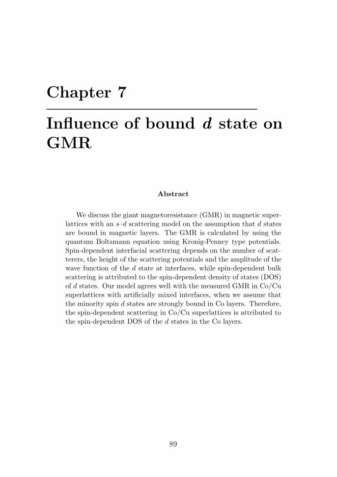
Chapter 7
Influence of bound d state onGMR
Abstract
We discuss the giant magnetoresistance (GMR) in magnetic super-lattices with an s–d scattering model on the assumption that d statesare bound in magnetic layers. The GMR is calculated by using thequantum Boltzmann equation using Kronig-Penney type potentials.Spin-dependent interfacial scattering depends on the number of scat-terers, the height of the scattering potentials and the amplitude of thewave function of the d state at interfaces, while spin-dependent bulkscattering is attributed to the spin-dependent density of states (DOS)of d states. Our model agrees well with the measured GMR in Co/Cusuperlattices with artificially mixed interfaces, when we assume thatthe minority spin d states are strongly bound in Co layers. Therefore,the spin-dependent scattering in Co/Cu superlattices is attributed tothe spin-dependent DOS of the d states in the Co layers.
89

90 Chapter 7. Influence of bound d state on GMR
7.1 Introduction
The giant magnetoresistance (GMR) exhibited in many magnetic superlat-
tices and granular alloys arises from the spin-dependent scattering of conduc-
tion electrons [1–5]. It has been pointed out that the interfacial scattering of
conduction electrons plays an important role in the spin-dependent scatter-
ing [1]. For M/Cu (M =Co, NiFe) systems, however, no one has reported
the enhancement of the GMR owing to the interfacial roughness [6–10]. In
Chapter 6 [7], we have reported that the spin-dependent bulk scattering is
important for the occurrence of the GMR. On the other hand, Parkin [11]
has reported that the GMR is enhanced by very thin Co layers inserted at
interfaces of NiFe/Cu multilayers. He claimed that the interfacial state as
well as roughness plays an important role in the GMR. These experimen-
tal results require a theory to take account of both the spin-dependent bulk
scattering and the interfacial electronic states.
For M/Cu systems, Edwards et al. [12] and Xing et al. [13, 14] insist on
the importance of a spin-dependent density of states (DOS) of d bands in
magnetic layers. In these models, the GMR is attributed to the scattering of
s electrons to unfilled d bands which have spin-dependent DOS. These mod-
els semi-quantitatively agree with the layer thickness dependence of GMR in
M/Cu systems. However, the influence of the interfacial state has not been
treated explicitly, since the Fermi surfaces of s and d bands are treated as
simple sphere. Recently, Schep et al. [15] calculated the GMR in a method
based on the full electronic structure. They reported the importance of the
s–d hybridization for the origin of the GMR in the current-perpendicular-
to-the-plane (CPP) geometry. However, their theory does not satisfactorily
7.2. Model 91
explain the considerable MR observed in the current-in-the-plane (CIP) ge-
ometry. They suggest that some additional scattering mechanism is necessary
for explaining the CIP MR.
In this chapter, we have extended the resistor network theory to include
the interfacial state explicitly, on the basis of the method developed by Viss-
cher [16]. The simple expression we have deduced neglecting the s–d hy-
bridization agrees well with our experimental results of the GMR observed
in CIP geometry for the Co/Cu superlattices with artificially mixed inter-
faces.
7.2 Model
We confine our discussions to low temperatures, neglect magnon and phonon
scattering and assume that the effective mean free path of the conduction
electrons is much larger than the superlattice period. This assumption limits
our discussion to scattering processes that do not cause spin mixing, so that
the current is carried separately by up- and down-spin conduction electrons
(two-current model) as [17]
ρ =ρ↑ρ↓
ρ↑ + ρ↓, (7.1)
where ρ↑ and ρ↓ are the resistivity of up- and down-spin channels, respec-
tively, and ρ is the total resistivity. We assume that the current is carried
only by s electrons and neglect the current carried by d electrons with heavy
effective mass. The non-zero residual resistivity is due to the scattering of s
electrons by impurities or defects at rSC with a potential of the form
V (r) = V0δ(r− rSC). (7.2)

92 Chapter 7. Influence of bound d state on GMR
In the transition metals, the s electrons can be scattered into holes in s band
(s–s scattering) or d band (s–d scattering) when they are scattered either
at interfaces or inside layers. The scattering rate of s–s and s–d scattering
will be determined by the scattering amplitude for the transition between an
initial and a final state and the availability of states into which the electrons
can be scattered. Since only electrons near Fermi surface contribute to the
resistivity, these scattering rate can be written in terms of Fermi’s golden
rule as
P σif =
2π
∣∣⟨Φσf |V (r)|Ψσ
i
⟩∣∣2 N(EF), (7.3)
where Ψσi and Φ
σf are an initial s and a final s or d state for the σ spin,
respectively, and N(EF) is the DOS of the final state at the Fermi energy
EF. The total scattering rate is the summation of the s–s and s–d scattering
rate. Therefore, the properties of s and d bands near the Fermi surface
play an important role in the GMR. We treat the s and d bands with the
effective-mass approximation. Since the CIP MR due to s–d hybridization is
small [15], we neglect it and assume that the bulk of each metal constituting
the superlattice has two free electron bands with different effective masses.
One corresponds to an s band, and another corresponds to a d band. The
effective masses and potentials for the bands may depend on spin directions
for the ferromagnetic metals. When two metals are layered alternately, the
superlattice states will be formed owing to the potential modulation. For
systems such asM/Cu, s electrons see small potential differences at interfaces
between magnetic and nonmagnetic layers, since the bottoms of s bands of
these metals are well aligned on the scale of the Fermi energy [18,19]. Owing
to the superlattice state due to the superlattice potential, the anisotropy in

7.2. Model 93
the Fermi wave number will arise. Although this anisotropy affects the CPP
MR, its influence on the CIP MR can be negligible [20]. This means that the
s states can be treated as simple plain waves when the potential differences
are small. For simplicity, we assume that s electrons do not see any potential
differences when crossing the interfaces between magnetic and non-magnetic
layers, since we are now interested in the CIP MR. On the other hand, d
states see a large potential difference at interfaces, since there is an exchange
interaction in ferromagnetic layers. Assuming the superlattice to be infinite
in the z direction, the superlattice potentials are modeled by Kronig-Penney-
type potentials. We assume that the potentials for the d states are constant
within each layer but depend on spin and material. For systems such as
M/Cu, the d band of Cu and the majority-spin d band of the ferromagnetic
layers lie well below the Fermi energy, so they do not contribute to the
resistivity [18, 19]. Therefore, we take account of only the minority-spin d
band of ferromagnetic layers. The potential for the d band is composed of a
periodic array of barriers of thickness a with height Ub and wells of thickness
b with depth Uw as shown in Fig. 7.1. For a ferromagnetic (F) configuration
of the magnetization of ferromagnetic layers, the potential for down-spin
electrons has a = tNM and b = tM, where tNM is the thickness of nonmagnetic
layers and tM of magnetic layers; for up-spin electrons, b = 0, i.e., there
are no wells. For antiferromagnetic (AF) configurations, the potentials for
up- and down-spin electrons are the same and are shifted in space relative
to one another; a = 2tNM + tM and b = tM. The potential for the s band
is at Us and is constant in a superlattice as mentioned above. For these
step-function potentials, we calculate the scattering matrix elements from
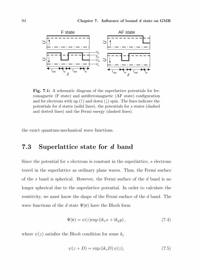
94 Chapter 7. Influence of bound d state on GMR
F state AF state
UU
ztNM
tNM
tM
tM
UwUs
EF
Ub
UU
ztNM
tNM
tM
tM
Fig. 7.1: A schematic diagram of the superlattice potentials for fer-romagnetic (F state) and antiferromagnetic (AF state) configurationand for electrons with up (↑) and down (↓) spin. The lines indicate thepotentials for d states (solid lines), the potentials for s states (dashedand dotted lines) and the Fermi energy (dashed lines).
the exact quantum-mechanical wave functions.
7.3 Superlattice state for d band
Since the potential for s electrons is constant in the superlattice, s electrons
travel in the superlattice as ordinary plane waves. Thus, the Fermi surface
of the s band is spherical. However, the Fermi surface of the d band is no
longer spherical due to the superlattice potential. In order to calculate the
resistivity, we must know the shape of the Fermi surface of the d band. The
wave functions of the d state Ψ(r) have the Bloch form
Ψ(r) = ψ(z)exp (ikxx + ikyy) , (7.4)
where ψ(z) satisfies the Bloch condition for some kz
ψ(z +D) = exp (ikzD)ψ(z), (7.5)

7.4. Calculation of resistivity 95
where D = a+ b. The Brillouin zone is infinite in the x and y directions, and
2π/D wide in z (kz) direction. Here, we normalize the wave function Ψ as
Ω−1
∫|Ψ(r)|2 d3r = 1, (7.6)
where Ω is the volume of a normalization box. The solution of ψ(z) is a
linear combination of exp(±ikLz), where kL on the Fermi surface is defined
in the well as
kL =
[2md
2(EF − Uw)− kr
2
]1/2
≡ K, (7.7)
and in the barrier as
kL =
[2md
2(EF − Ub)− kr
2
]1/2
≡ iQ, (7.8)
where kr =(kx
2 + ky2)1/2
and md is the effective mass of the d states. From
Eq. (7.5) and the boundary conditions where ψ and dψ/dz are continuous,
we obtain
eQb
2
[Q2 −K2
2QKsin (Ka) + cos (Ka)
]= cos (kzD). (7.9)
In this study, we consider a case in which the barrier height is large enough
to satisfy eQb1. In this case, the minority-spin d states are confined to the
magnetic layers and have eigenstates quantized to the thickness of magnetic
layers. Therefore, the Fermi surface becomes a set of cylinders (subbands)
parallel to the z (or kz) direction.
7.4 Calculation of resistivity
Resistivities are calculated by the relaxation time approximation of the Boltz-
mann equation. Since we neglect the shift of the Fermi surface for the d
96 Chapter 7. Influence of bound d state on GMR
states, the relaxation time τσ(k) (σ = ↑, ↓) is given as [13, 14, 17]
1
τσ(k)=
1
τ ssσ (k)
+1
τ sdσ (k)
, (7.10)
1
τ ssσ (k)
=
∫ (1− k · k′
k2
)P (k′sσ,ksσ)d3k′, (7.11)
1
τ sdσ (k)
=
∫P (k′dσ,ksσ)d3k′, (7.12)
where P (k′i,kj) is the scattering rate between states (k′i) and (kj), i and
j stand for s↑, s↓, d↑ and d↓. The first term in Eq. (7.10) comes from s–s
scattering, and the second from s–d scattering. For simplicity, we assume
here that the bulk scatterers with the potential strength V0 = VB distribute
in the superlattices with uniform volume density of ηB. In addition, we
assume that the interfacial scatterers with the potential strength V0 = VI
distribute within the region of z = zi ± ε with the uniform volume density of
ηI, where zi is the position of the ith interface. Here, we do not assume any
spin dependence in VB and VI as in [12] and [13, 14].
7.4.1 s–s scattering
Since the wave function of the s state is a plane wave, it is easy to calculate
the rate of s–s scattering. Using Fermi’s golden rule, the scattering rate is
given as [16]
P (k′sσ,ksσ)d3k′ =2π
(VB
2ηB + nssI
2ε
DVI
2ηI
)dN(EF), (7.13)
where nssI is the number of interfaces in a period of superlattice potential
and dN(EF) denotes the number of states per unit volume and unit energy
at EF in the volume element d3k′ near k′. Integrating Eq. (7.13), we obtain

7.4. Calculation of resistivity 97
the relaxation time due to s–s scattering as
1
τ ssσ
=2π
gs(EF)
(VB
2ηB + nssI
2ε
DVI
2ηI
), (7.14)
gs(EF) =msk
sF
2π22, (7.15)
where ms and ksF are the effective mass and the Fermi wave number of s
electrons. The first term in the parentheses of Eq. (7.14) comes from the
bulk scattering, while the second term is due to the interfacial scattering.
7.4.2 s–d scattering
The scattering rate of s–d scattering is written as
P (k′dσ,ksσ)d3k′ =2π
(VB
2ηB +∑
i
2ε|ψk′(zi)|2D
VI2ηI
)dN(EF), (7.16)
when ε2π/k′. The summation in Eq. (7.16) is taken over the interfaces
in a period of the superlattice potential. In the case of Qb1, d states are
confined in the well layers, so the amplitude of ψk′(z) has a non-zero value
in the well layers and near the interfaces between the well and the barrier
layers. Thus, it is enough to take the summation in Eq. (7.16) over the well-
barrier interfaces. From the analogy with the simple quantum well problem,
|ψk′(zi)|2 has the same value at the interfaces as at both edges of the welllayers. Hence, Eq. (7.16) is written with the number of the well-barrier
interfaces in a period nsdI as
P (k′dσ,ksσ)d3k′ =2π
(VB
2ηB + nsdI
2ε|ψk′(zI)|2D
VI2ηI
)dN(EF), (7.17)
where zI is the position of one of the interfaces causing non-zero s–d scat-
tering. As mentioned in the previous section, allowed-wave-number vectors

98 Chapter 7. Influence of bound d state on GMR
k′ are discrete. In each subband, the value of k′r and the wave function are
constant, since Qb 1. Thus, we obtain
dN(EF) =md
(2π)2dk′
z, (7.18)
for each subband, where dk′z is a length increment along the Fermi surface in
the z direction. Integrating Eq. (7.17) using Eq. (7.18), the relaxation time
due to s–d scattering is given with the k′r in the jth subband k′rj as
1
τ sdσ
=2π
gd(EF)
a
D
(VB
2ηB + nsdI
2εφ
DVI
2ηI
), (7.19)
φ =1
nd
nd∑j=1
∣∣ψk′r
j (zI)∣∣2 , (7.20)
gd(EF) =mdnd
2π2a, (7.21)
where nd is the number of d subbands. The first term in the parentheses
of Eq. (7.19) comes from the bulk scattering, while the second term is due
to the interfacial scattering. Since the relaxation time due to both s–s and
s–d scattering [Eqs. (7.14) and (7.19)] is independent of k, the resistivity is
written with the density of s electrons Ns as
ρσ =2πms
Nse2
gs(EF)
(VB
2ηB + nssI
2ε
DVI
2ηI
)
+ gd(EF)a
D
(VB
2ηB + nsdI
2εφ
DVI
2ηI
). (7.22)
Equation (7.15) indicates that gs(EF) is the DOS of the s states per
spin at the Fermi energy for the bulk. On the other hand, gd(EF) de-
pends on nd due to the quantum size effect. When the barrier height Ub
is large enough, nd is approximated by the maximum integer satisfying
nd ≤ (a/π) [2md(EF − Uw)/2]
1/2. If we neglect the discreteness in nd, gd(EF)

7.5. GMR 99
is identical with the DOS of the d states at the Fermi energy for the bulk fer-
romagnetic metals. In this case, Eq. (7.22) has the same form as the resistor
network theory except for the terms due to the interfacial scattering. The
interfacial scattering depends on the number of the scattering centers (2εηI),
the strength of the scattering potential (VI) and the amplitude of the wave
function of the d state at interfaces (|ψk(zI)|2). The first one correspondsto the magnitude of the interfacial roughness, and the last one corresponds
to interfacial electronic state. Therefore, our model includes not only the
interfacial roughness but also the interfacial electronic states.
7.5 GMR
In this section, we calculate the GMR using Eq. (7.22). The parameters
dependent on the spin and magnetic configuration are D, nssI , n
sdI and φ.
Defining the superlattice period as λ = tM + tNM, the value of D for the F
state is λ and that for the AF state is 2λ. According to this, the value of
nssI for the F state is 2, and that for the AF state is 4. The values of nsd
I
for the down-spin electrons for the F state and for the up- and down-spin
electrons for the AF state are 2, while nsdI = 0 for up-spin electrons for the F
state. Since the normalization condition depends on the superlattice period
(see Eq. (7.6)), φ for the AF state is two times larger than that for the F
state. Thus, φ = 2φF for the AF state, where φF is the φ for the F state. The
number of the subbands nd is constant, unless the thickness of the magnetic
layers changes. With these parameters, we obtain the expressions for the

100 Chapter 7. Influence of bound d state on GMR
spin-dependent resistivities for the F state ρFσ as
ρF↑ =
2πms
Nse2
[gs(EF)
(VB
2ηB +4ε
λVI
2ηI
)], (7.23)
ρF↓ =
2πms
Nse2
[gs(EF)
(VB
2ηB +4ε
λVI
2ηI
)
+ gd(EF)tMλ
(VB
2ηB +4εφF
λVI
2ηI
)], (7.24)
and the resistivities for the AF state ρAFσ as
ρAF↑ = ρAF
↓
=2πms
Nse2
[gs(EF)
(VB
2ηB +4ε
λVI
2ηI
)
+ gd(EF)tM2λ
(VB
2ηB +4εφF
λVI
2ηI
)]. (7.25)
Although the GMR can be calculated numerically assuming the appro-
priate superlattice potentials, here we discuss the GMR phenomenologically,
treating gd(EF) and φF as independent parameters for better transparency
in the physics. Figure 7.2 shows the calculated MR ratio with respect to 2ε
and φF. We assume here that tM = 1 nm, tNM = 2 nm, gd(EF)/gs(EF) = 12
and VI2ηI/VB
2ηB = 5. These values are suitable for explaining the experi-
mental results for Co/Cu superlattices, as we mention in the next section.
A considerable MR ratio is obtained even without the interfacial scattering
(2ε = 0 nm) because of the strong spin dependence in the DOS of the d
states. The MR ratio decreases with increasing 2ε for φF 1, while it in-
creases with increasing 2ε for φF 1. This tendency remains unchanged if
we use different values for the layer thicknesses, the ratios of the DOS and
the interfacial to bulk scattering. Thus, the relationship between the MR

7.5. GMR 101
01
23
0.0
0.1
0.2
0.3
2.0
1.5
1.0
0.5
0.0
MR
rat
io
MR
rat
io
0.0
0.5
1.0
1.5
2.0
0.30.20.10.0
2ε (nm)
φF
Fig. 7.2: Calculated MR ratio with respect to 2ε and φF. The param-eters are assumed to be tM = 1 nm, tNM = 2 nm, gd(EF)/gs(EF) = 12and VI
2ηI/VB2ηB = 5. The regions of φF < 1 and φF > 1 are indicated
by the different tones.
ratio and the interfacial roughness strongly depends on φF. In other words,
the GMR in superlattices with interfacial roughness strongly depends on the
amplitude of the wave function of the d state at interfaces. In the next sec-
tion, we estimate the magnitude of φF for Co/Cu superlattices by comparing
our calculation with experiments.
102 Chapter 7. Influence of bound d state on GMR
7.6 Interfacial scattering in Co/Cu
We have reported the structure and the GMR properties of Co/Cu superlat-
tices with artificially mixed interfaces in Chapters 4–6 [6,7,21]. The interfaces
in Co/Cu have been modified by codeposition. The Co and Cu atoms are
mixing randomly in the interfacial regions, which increases with increasing
nominal thickness of the codeposited region tmix.
The resistivity of these samples decreases from the initial value at zero
field with increasing magnetic field, and saturates at the value of ρs(=ρF)
in a field larger than the saturation field. After saturation, the resistivity
has a peak near the coercive field. Since the value of the initial resistivity is
larger than that of the peak one, the AF alignment of the magnetization of
the Co layers is closer to perfection in the initial state than that in the field
where the resistivity has the peak. The magnetization of all samples is zero
in initial state, and the relationship between the resistivity and the square
of the magnetization is linear at low temperatures. From the discussion
in Chapter 6, this indicates that magnetic configuration of our samples is
very close to the perfect AF alignment at the initial state. Therefore we
denote the resistivity in the initial states as ρAF here. Furthermore, linear
dependence of the resistivity on the square of the magnetization precludes
the strong spin dependence of the scattering potential for both bulk and
interfacial scattering.
Figure 7.3 shows the tmix dependence of the GMR measured at 5 K for
[Co(1.0nm)/Cu(2.2nm)]16. Data are taken from Chapter 6 [7]. Both ρAF and
ρF increase with increasing tmix, while the MR ratio decreases. It is clear that
the interfacial scattering is crucial but less spin dependent.
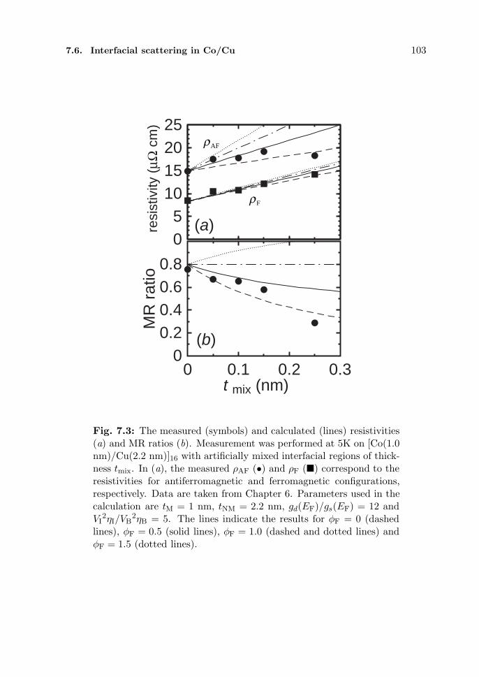
7.6. Interfacial scattering in Co/Cu 103
05
10152025
resi
stiv
ity (
µΩ c
m)
t mix (nm)
00.20.40.60.8
0 0.1 0.2 0.3
MR
rat
io
(b)
(a)
ρAF
ρF
Fig. 7.3: The measured (symbols) and calculated (lines) resistivities(a) and MR ratios (b). Measurement was performed at 5K on [Co(1.0nm)/Cu(2.2 nm)]16 with artificially mixed interfacial regions of thick-ness tmix. In (a), the measured ρAF (•) and ρF () correspond to theresistivities for antiferromagnetic and ferromagnetic configurations,respectively. Data are taken from Chapter 6. Parameters used in thecalculation are tM = 1 nm, tNM = 2.2 nm, gd(EF)/gs(EF) = 12 andVI
2ηI/VB2ηB = 5. The lines indicate the results for φF = 0 (dashed
lines), φF = 0.5 (solid lines), φF = 1.0 (dashed and dotted lines) andφF = 1.5 (dotted lines).
104 Chapter 7. Influence of bound d state on GMR
Despite the large difference in the resistivities at low temperature, no
significant differences in the temperature dependence of the GMR between
the samples with different tmix have been observed (see Figs. 6.3–6.6 ). For
all samples, ρF closely approximates a T 2 power law, while ρAF − ρF changes
linearly with T 3/2. The difference between the temperature coefficients of
the samples of tmix 0.15 nm is small. This indicates that the interfacial
scattering can be attributed to the impurity or defect scattering.
Although the mean free path roughly estimated for the maximum resis-
tivity in Fig. 7.3 (≈ 20µΩ cm) is about 4.0 nm, Edwards et al. [12] indicated
that the limit of long mean free path is already reached rapidly for a mean
free path comparable with the superlattice period. Therefore, it is appro-
priate to adopt the present model for interpreting the tmix dependence of
the GMR at 5 K. We can estimate the value of gd(EF)/gs(EF) at about 12
from the measured MR ratio of the sample of tmix = 0 nm, if we neglect the
interfacial scattering [assuming ε = 0 nm in equations (7.23)–(7.25)]. This
value of gd(EF)/gs(EF) is close to the ratio of the calculated DOS at EF in
the majority- and minority-spin bands in bulk Co [18,19]. The calculated re-
sistivities and the MR ratio for the parameters of tM = 1 nm, tNM = 2.2 nm,
gd(EF)/gs(EF) = 12 and VI2ηI/VB
2ηB = 5 are also indicated by lines in Fig.
7.3, where we assume that tmix = 2ε. The calculated results are normalized
at tmix = 0 so as to make the calculated ρF equal to the measured one. It
is clear that the behavior of ρF is insensitive to φF. The agreement between
measured and calculated ρF is good when VI2ηI/VB
2ηB = 5.0± 1.0. It is rea-sonable that the density of the scattering centers is larger, or the scattering
potential is stronger at interfaces than in the bulk (ηI > ηB or VI > VB).

7.6. Interfacial scattering in Co/Cu 105
On the other hand, ρAF is sensitive to φF. Comparing the measured and the
calculated results, φF0.5 is suitable for explaining the behavior of ρAF and
the MR ratio for the samples for which tmix 0.15 nm. The approximation
of ε2π/k′ in Eq. (7.16) will no longer hold when tmix becomes comparable
with the period of |ψk(z)|2. This affect ρAF much more than it does ρF,
and may cause the deviation between the measured and calculated ρAF at
tmix = 0.25 nm. Detailed numerical calculation will be necessary to study
the GMR for the samples with such large roughness. The value of φF < 1
indicates that amplitude of the d states is attenuated at interfaces, since the
average value of |ψk(z)|2 is about λ/tM (> 1) in the magnetic layers. Thus,
d states are strongly bound in magnetic layers.
Our model agrees well with the experimental results. However, the con-
tribution of the interfacial scattering to the resistivity of the sample with
tmix = 0 nm remains unclear, although we neglect it in the above discussion.
In fact, we have confirmed the existence of a small amount of interfacial mix-
ing for the sample with tmix = 0 nm (see Chapter 4 and reference [21]). The
influence of the interfacial mixing can also be discussed by the layer thick-
ness dependence of the resistivities. Thus, we focus our attention on the
dependence of ρF (which is not influenced by the interlayer coupling between
adjacent Co layers) on the thickness of the Co and Cu layers for samples with-
out intentionally mixed interfaces. As a result, ρF increases with increasing
Co layer thickness, while it decreases with increasing Cu layer thickness. This
indicates clearly that the resistivity of Co layers is larger than that of not
only Cu layers but also the interfaces. This layer thickness dependence is
reproduced only when ε is very small in Eqs. (7.23) and (7.24). Therefore,

106 Chapter 7. Influence of bound d state on GMR
our assumption of ε = 0 for the sample with tmix = 0 nm is appropriate.
If superlattices have slightly rougher interfaces than those of our samples
with tmix = 0 nm, the interfacial scattering will influence the GMR signifi-
cantly depending on the interfacial electronic state. The interfacial electronic
state should be sensitive to the combination of metals. Parkin [11] has re-
ported that the MR ratio is enhanced by inserting very thin Co layers at
the interfaces between Cu and NiFe layers. This can be interpreted in our
model as the change in φF depending on materials. The virtual bound state
indicated by Inoue and Maekawa [22] may also affect the magnitude of the
GMR. However, the bulk s–d scattering will be the most important process
giving rise to the GMR in M/Cu superlattices, since a very large MR ratio
is observed, at least for our sample whose interfacial scattering is very small.
Consequently, the GMR in Co/Cu superlattices mainly comes from the
spin-dependent bulk scattering due to spin-dependent DOS in the Co layers.
The interfacial scattering due to interfacial roughness is less spin dependent
than the bulk scattering. This is understood in terms of the d states bound
in the Co layers.
7.7 Conclusion
We have extended the resistor network theory to include the interfacial scat-
tering explicitly and discussed the role of bound d state in the CIP MR.
The interfacial states are described in our model with the number of inter-
facial scattering centers (2εηI), the height of the scattering potentials (VI)
and the amplitude of the wave function of the d states (|ψk(zI)|2). The firstis concerned with the interfacial roughness, and the last corresponds to the
References 107
interfacial electronic state. Our model is consistent with the experiments for
Co/Cu superlattices with artificially mixed interfaces, when we assume that
the minority spin d states are strongly bound in Co layers. Therefore, the
GMR in Co/Cu superlattices mainly comes from the spin-dependent s–d scat-
tering in the Co layers, and the interfacial scattering is less spin-dependent
than bulk scattering. This is because of the attenuation of the wave function
of d states at interfaces.
References
[1] M. N. Baibich, J. M. Broto, A. Fert, F. Nguyen Van Dau, F. Petroff, P.
Etienne, G. Creuzet, A. Friederich, and J. Chazelas, Phys. Rev. Lett.
61, 2472 (1988).
[2] S. S. P. Parkin, R. Bhadra, and K. P. Roche, Phys. Rev. Lett. 66, 2152
(1991).
[3] D. H. Mosca, F. Petroff, A. Fert, P. A. Schroeder, W. P. Pratt Jr., and
R. Laloee, J. Magn. Magn. Mater. 94, L1 (1991).
[4] A. E. Berkowitz, J. R. Mitchell, M. J. Carey, A. P. Young, S. Zhang,
F. E. Spada, F. T. Parker, A. Hutten, and G. Thomas, Phys. Rev. Lett.
68, 3745 (1992).
[5] J. Q. Xiao, J. Samuel, and L. Chien, Phys. Rev. Lett. 68, 3749 (1992).
[6] M. Suzuki and Y. Taga, J. Appl. Phys. 74, 4660 (1993).
[7] M. Suzuki and Y. Taga, Phys. Rev. B 52, 361 (1995).
108 Chapter 7. Influence of bound d state on GMR
[8] V. S. Speriosu, J. P. Nozieres, B. A. Gurney, B. Dieny, T. C. Huang,
and H. Lefakis, Phys. Rev. B 47, 11579 (1993).
[9] M. J. Hall, B. J. Hickey, M. A. Howson, C. Hammond, M. J. Walker,
D. G. Wright, D. Greig, and N. Wiser, J. Phys. Condens. Mater. 4, L495
(1992).
[10] T. Thomson, P. C. Riedi, and D. Greig, Phys. Rev. B 50, 10319 (1994).
[11] S. S. P. Parkin, Phys. Rev. Lett. 71, 1641 (1993).
[12] D. M. Edwards, J. Mathon, and R. B. Muniz, IEEE Trans. Magn. 27,
3548 (1991).
[13] L. Xing and Y. C. Chang, Phys. Rev. B 48, 4156 (1993).
[14] L. Xing, Y. C. Chang, M. B. Salamon, D. M. Frenkel, J. Shi, and J. P.
Lu, Phys. Rev. B 48, 6728 (1993).
[15] K. M. Schep, P. J. Kelly, and G. E. W. Bauer, Phys. Rev. Lett. 74, 586
(1995).
[16] P. B. Visscher, Phys. Rev. B 49, 3907 (1994).
[17] A. Fert and I. A. Campbell, J. Phys. C 6, 849 (1976).
[18] R. A. Ballinger and C. A. W. Marshall, J. Phys. F 3, 735 (1973).
[19] M. Mehta-Ajmani, I. P. Batra, E. E. Lafon, and C. S. Fadley, J. Phys.
C 13, 2807 (1980).
[20] S. Zhang and P. M. Levy, in Mat. Res. Soc. Symp. Proc., Vol. 313, p.
53.

References 109
[21] M. Suzuki, Y. Taga, A. Goto, and H. Yasuoka, Phys. Rev. B 50, 18580
(1994).
[22] J. Inoue and S. Maekawa, J. Phys. Soc. Jpn. 61, 1149 (1992).

Chapter 8
GMR sensors using Co/Cusuperlattices
Abstract
We have demonstrated the usefulness of giant magnetoresistance(GMR) in Co/Cu superlattices for practical application to the mag-netic rotation sensor. Optimized Co/Cu superlattices have been fab-ricated into sensors with appropriate passivation layers. The sensoroutput changes more than 20%, synchronizing the rotation of the mag-net rotor. It is remarkable that there is no significant degradation ofthe GMR sensors even after they are left in the atmosphere of theair at 150 C for 1000 h. This confirms the high reliability of theGMR sensors and promises that they can be used in automobiles andaircraft under sever conditions.
111

112 Chapter 8. GMR sensors using Co/Cu superlattices
8.1 Introduction
Giant magnetoresistance (GMR), first found in magnetic superlattices [1–3],
has attracted much attention from both fundamental and practical stand-
points. For a large change in the resistance, antiferromagnetic (AF) align-
ment of the magnetization of adjacent magnetic layers is essential. In super-
lattices with GMR, the AF alignment is realized by means of AF exchange
coupling through the nonmagnetic layers. Since the AF coupling is rather
strong, it is difficult to improve the sensitivity of the GMR to the magnetic
field, despite its large magnetoresistance (MR) ratio. In order to overcome
this difficulty, an uncoupled magnetic sandwich structure, the so-called spin
valve, has been proposed [4–7]. In the spin valve structure, the magnetization
of magnetic layers is aligned antiferromagnetically by pinning the magneti-
zation of one of the ferromagnetic layers using the exchange-biasing layer.
Since the spin valve shows an MR ratio of more than 5% in a few Oe, this
device is expected to find the application to the MR head, MR memory, etc.
Therefore, most of the recent industrial interest is focused on the application
of spin valve GMR for high density data storage.
On the other hand, various commercial MR sensors using conventional
MR such as NiFe and NiCo are available on the market. These sensors are
used practically in rotation, angular and position sensing. For certain uses,
it has been required to enlarge the sensor output rather than enhance the
sensitivity to the magnetic field. In such cases, conventional MR sensors can
be replaced by GMR sensors of the superlattice type (not spin valve) from
the following points of view. (1) Generally, superlattice GMR sensors can
produce a larger signal than spin valve and conventional MR sensors. (2)

8.2. Experiments 113
They are strongly resistant to electromagnetic interference; this is consistent
with the low sensitivity of the superlattice GMR to the magnetic field. (3)
The preparation of the superlattices is easier than that of spin valve, resulting
in high production throughput. Therefore, GMR superlattice sensors have
many advantages for application to rotation, angular and position sensing in
such as automobiles and aircraft.
However, there has been a prejudice that superlattices may not be durable
enough to be used under such sever conditions. In fact, it has been reported
that the MR ratio of Co/Cu superlattices is decreased significantly by anneal-
ing at a temperature of 250–300 C [8], while it is not changed by annealing
at 150 C [9]. In these studies, Co/Cu superlattices were annealed in the
high vacuum for only a few hours. Contrary to this, for practical sensors,
durability for a much longer period in air is required. Up to now, there have
been no reports on the thermal durability of superlattices in air for a long
period.
The purpose of this chapter is to clarify the usefulness of the GMR su-
perlattice sensors for the practical application to the rotation sensors. We
focused our attention on Co/Cu superlattices and refined their GMR prop-
erties. Furthermore, we fabricated simple GMR sensors and evaluated the
performance and their durability in air.
8.2 Experiments
The Co/Cu superlattices were deposited on surface-oxidized Si substrates in
a magnetron sputtering system with a base pressure of 2×10⁻⁷ Torr. After
deposition of a buffer layer, 16–24 Co/Cu bilayers were grown at room tem-

114 Chapter 8. GMR sensors using Co/Cu superlattices
perature in an Ar pressure of 3×10⁻³ Torr at a deposition rate of 0.2 − 0.3
nm/s.
As described in Chapter 3, we optimized the GMR properties in Co/Cu
superlattices for the application to the sensors by changing the combination
of the layer thicknesses of Co and Cu. Moreover, the crystallographic ori-
entation and interfacial roughness are controlled by changing the thickness
and the substance of the buffer layer to archive a large MR ratio and a small
saturation field.
Using the optimized Co/Cu superlattices with a structure of NiFe(5.0
nm)/Cu(2.1 nm)/[Co(1.0 nm)/Cu(2.1 nm)/]16, we fabricated the magnetic
field sensors. The structure of the GMR sensors is shown in Fig. 8.1. Since
the MR ratio of Co/Cu superlattices (∼ 20%) is much larger than that
of conventional MR in such as NiFe or NiCo (∼ 3%), and the resistivity of
Co/Cu superlattices is comparable with that of NiFe and NiCo, the structure
of the GMR sensor element can be very much simpler. In this work, we
fabricated a sensing element of 45 µm width and 4.2 mm length in an area of
3 × 5mm2. To locate the sensing element close to the magnet, element was
patterned at 300 µm from the edge of the sensor chip.
The fabrication process is as follows. After the optimized Co/Cu super-
lattices are deposited on the surface-oxidized Si wafer, they are patterned by
the laser trimming apparatus. The sensing element is insulated from the sur-
rounding superlattice by a laser-trimmed line of width 2 µm. As described
in Sec 8.3.3, Co/Cu superlattices are easily oxidized in high temperature air.
Moreover, they corrode in water containing ions. We must take care not to
expose the bare superlattice to high temperature air or to water during the

8.2. Experiments 115
Al electrodes
45 µ
m
4.2 mm
3 m
m
5 mm
contact holes
A
sensing element(a)
0.3
mm
AAAAAAAAAAAAl electrode
substrate(SiO2)
substrate(Si)
AAA AAA
laser-trimed line
Co/Cu supelattice
passivation (SiO2)laser-trimed line
(b)
Fig. 8.1: Schematic structure of the GMR sensor element. (a) Topview (b) cross-sectional view along the broken line A in (a).
fabrication process. Laser trimming enables us to pattern the superlattice
without heating or using water, both of which are necessary for standard
photolithography.
On the patterned superlattices, SiO2 was deposited as a passivation layer
by sputtering at room temperature in an Ar pressure of 3×10⁻³ Torr at a
deposition rate of 0.3 nm/s up to a thickness of 800 nm. The contact holes
are formed by standard photolithography and reactive ion etching (RIE) with
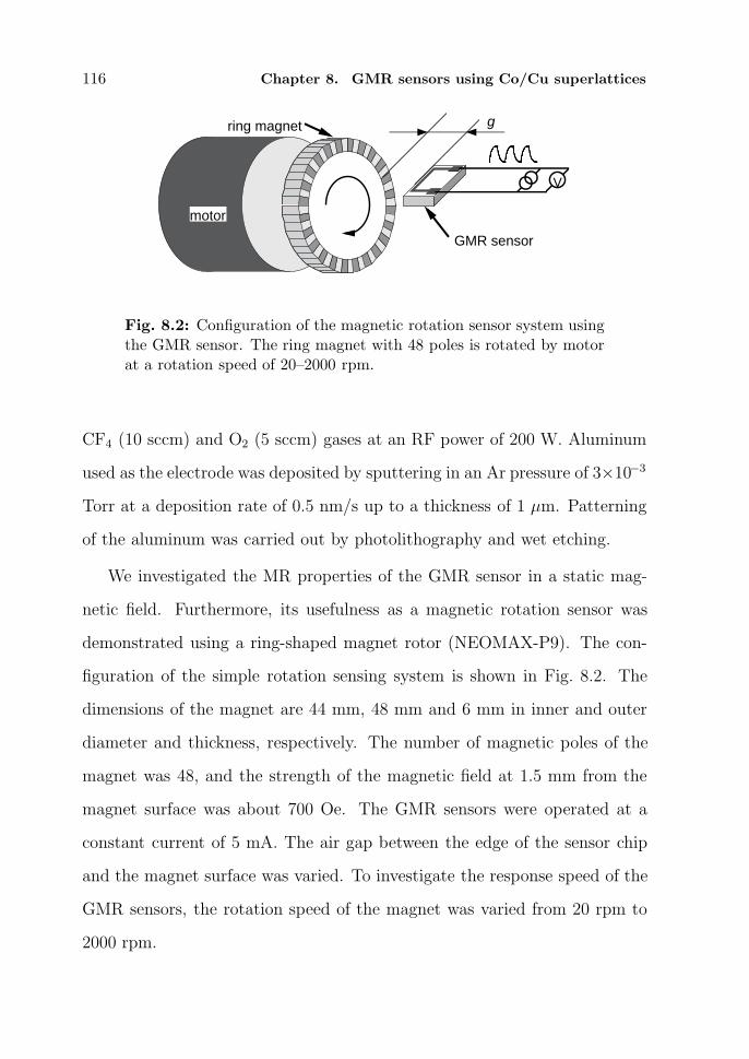
116 Chapter 8. GMR sensors using Co/Cu superlattices
ring magnet
V
g
GMR sensor
motor
Fig. 8.2: Configuration of the magnetic rotation sensor system usingthe GMR sensor. The ring magnet with 48 poles is rotated by motorat a rotation speed of 20–2000 rpm.
CF4 (10 sccm) and O2 (5 sccm) gases at an RF power of 200 W. Aluminum
used as the electrode was deposited by sputtering in an Ar pressure of 3×10⁻³
Torr at a deposition rate of 0.5 nm/s up to a thickness of 1 µm. Patterning
of the aluminum was carried out by photolithography and wet etching.
We investigated the MR properties of the GMR sensor in a static mag-
netic field. Furthermore, its usefulness as a magnetic rotation sensor was
demonstrated using a ring-shaped magnet rotor (NEOMAX-P9). The con-
figuration of the simple rotation sensing system is shown in Fig. 8.2. The
dimensions of the magnet are 44 mm, 48 mm and 6 mm in inner and outer
diameter and thickness, respectively. The number of magnetic poles of the
magnet was 48, and the strength of the magnetic field at 1.5 mm from the
magnet surface was about 700 Oe. The GMR sensors were operated at a
constant current of 5 mA. The air gap between the edge of the sensor chip
and the magnet surface was varied. To investigate the response speed of the
GMR sensors, the rotation speed of the magnet was varied from 20 rpm to
2000 rpm.
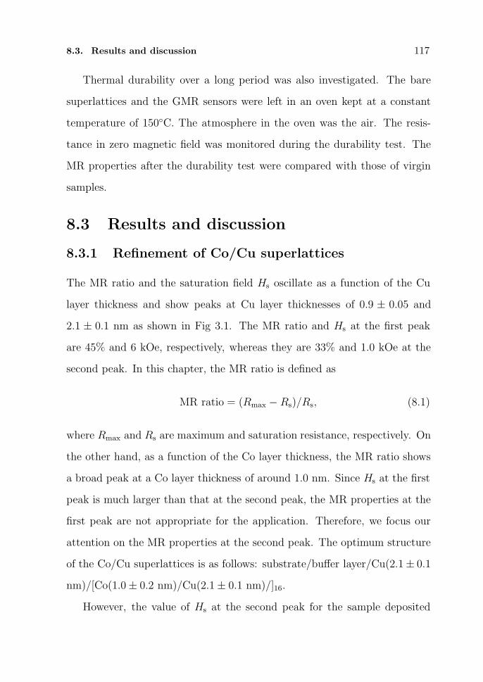
8.3. Results and discussion 117
Thermal durability over a long period was also investigated. The bare
superlattices and the GMR sensors were left in an oven kept at a constant
temperature of 150C. The atmosphere in the oven was the air. The resis-
tance in zero magnetic field was monitored during the durability test. The
MR properties after the durability test were compared with those of virgin
samples.
8.3 Results and discussion
8.3.1 Refinement of Co/Cu superlattices
The MR ratio and the saturation field Hs oscillate as a function of the Cu
layer thickness and show peaks at Cu layer thicknesses of 0.9 ± 0.05 and
2.1 ± 0.1 nm as shown in Fig 3.1. The MR ratio and Hs at the first peak
are 45% and 6 kOe, respectively, whereas they are 33% and 1.0 kOe at the
second peak. In this chapter, the MR ratio is defined as
MR ratio = (Rmax − Rs)/Rs, (8.1)
where Rmax and Rs are maximum and saturation resistance, respectively. On
the other hand, as a function of the Co layer thickness, the MR ratio shows
a broad peak at a Co layer thickness of around 1.0 nm. Since Hs at the first
peak is much larger than that at the second peak, the MR properties at the
first peak are not appropriate for the application. Therefore, we focus our
attention on the MR properties at the second peak. The optimum structure
of the Co/Cu superlattices is as follows: substrate/buffer layer/Cu(2.1± 0.1nm)/[Co(1.0± 0.2 nm)/Cu(2.1± 0.1 nm)/]16.
However, the value of Hs at the second peak for the sample deposited

118 Chapter 8. GMR sensors using Co/Cu superlattices
on the Fe buffer layer of thickness 5.0 nm is still too large for the practical
application. As we reported in the previous chapters, the MR properties
are closely related to the crystallographic preferred orientation of the Co/Cu
superlattice (see Chapter 3 and Ref. [10]), and the interfacial roughness (see
Chapters 4–6 and Refs. [11–13]). These can be controlled by changing the
thickness and the substance of the buffer layer. As indicated in Table 3.1,
the samples with (111) preferred orientation have small Hs and are more
appropriate for application than those with (110) preferred orientation. For
the samples with (111) orientation, however, the magnitude of the MR ratio
varies from 4% to 25% depending strongly on the substance of the buffer
layer. The difference in the MR ratio can be attributed to the magnitude
of the mesoscopic interfacial roughness. Among the substances we surveyed,
NiFe alloy is the best buffer layer, since Co/Cu superlattices deposited on
the thin NiFe layer show a large MR ratio (24.5%) and a small Hs (∼ 500
Oe), as indicated in Fig. 8.3(a).
On the basis of these results, we fabricated useful GMR sensors using
Cu(2.1 nm)/[Co(1.0 nm)/Cu(2.1 nm)/]16 superlattices deposited on the NiFe
buffer layer of thickness 5.0 nm. Their properties are discussed in the follow-
ing sections.
8.3.2 Characteristics of GMR sensors
Figure 8.3(b) shows the MR curves measured in the static magnetic field
for the GMR sensors. The values of Rmax and Rs are 346 Ω and 274 Ω,
respectively, and the MR ratio is 26.3%. The resistivities estimated from the
dimension of the sensing element are close to the values of the original super-

8.3. Results and discussion 119
-2 -1 0 1 2H (kOe)
(c)
-2 -1 0 1 2H (kOe)
(b)
0
5
10
15
20
25
30
-2 -1 0 1 2
MR
rat
io (
%)
H (kOe)
(a)
Fig. 8.3: The MR curves measured in the static magnetic fieldof (a) the optimum Co/Cu superlattice: substrate/NiFe(5.0)/Cu(2.1nm)/[Co(1.0 nm)/Cu(2.1 nm)]16; (b) the initial MR curve of the sen-sor (Sec. 8.3.2); and (c) the MR curve of the sensor measured afterthe durability test (Sec. 8.3.3). Sensors were fabricated using the su-perlattices with the same structure as (a).
lattices. We find small differences in MR properties between the GMR sensors
and the original superlattices. These are related to the fact that the Co/Cu
superlattices experience the high temperature process of photolithography.
During the fabrication of GMR sensors, the Co/Cu superlattices experience
the photolithography processes twice, for the patterning of the contact holes
and the Al electrodes. In each photolithography process, the superlattices
are heated in air up to 90 C and 120 C for the pre- and postbaking of the
resist, respectively, for 30 min. Nevertheless, the GMR sensors keep their
large MR ratio of 26.3% and their Hs are about 500 Oe. The differences in
MR ratio and Hs between the GMR sensors and the original superlattices
are not significant. It is clear that the MR properties of the GMR sensors
are still useful even after fabrication.
As described in Sec. 8.3.3, the MR ratio decreases significantly (to less
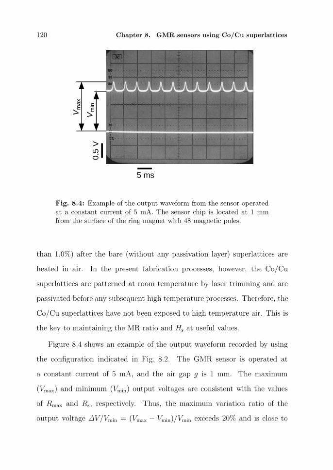
120 Chapter 8. GMR sensors using Co/Cu superlattices
Vm
ax
Vm
in
5 ms
0.5
V
Fig. 8.4: Example of the output waveform from the sensor operatedat a constant current of 5 mA. The sensor chip is located at 1 mmfrom the surface of the ring magnet with 48 magnetic poles.
than 1.0%) after the bare (without any passivation layer) superlattices are
heated in air. In the present fabrication processes, however, the Co/Cu
superlattices are patterned at room temperature by laser trimming and are
passivated before any subsequent high temperature processes. Therefore, the
Co/Cu superlattices have not been exposed to high temperature air. This is
the key to maintaining the MR ratio and Hs at useful values.
Figure 8.4 shows an example of the output waveform recorded by using
the configuration indicated in Fig. 8.2. The GMR sensor is operated at
a constant current of 5 mA, and the air gap g is 1 mm. The maximum
(Vmax) and minimum (Vmin) output voltages are consistent with the values
of Rmax and Rs, respectively. Thus, the maximum variation ratio of the
output voltage ∆V/Vmin = (Vmax − Vmin)/Vmin exceeds 20% and is close to
8.3. Results and discussion 121
the MR ratio measured in the static field. It is remarkable that the large ∆V
is available when using the very simple sensing element with considerable
low resistance (∼ 300Ω). If one expects conventional MR sensors such as
NiFe and NiCo to produce ∆V comparable with the present GMR sensor, a
sensing element with a resistance of ∼ 1.8 kΩ is required because of the small
MR ratio of ∼ 3%. Thus, the sensing element for conventional MR sensors
occupies a 6–10 times larger area than for GMR sensors. In other words,
GMR sensors can detect the variation of the magnetic field over a smaller
area than conventional MR sensors. As a result, the magnet rotor can be
reduced in size, and the number of the magnetic poles can be increased. This
leads to a significant improvement of the rotation sensing system, especially
in compactness and in capability to detect low rotation speed.
For practical applications, it is important to clarify the response speed
and the relation between the sensor output and g. Figure 8.5 shows the rela-
tionship between the value of g and the sensor output measured at rotation
speeds of 20, 200, 2000 rpm. At g ≤ 2.0 mm, the value of ∆V/Vmin exceeds
20% at all rotation speeds, whereas it decreases significantly at g > 2.0 mm.
Figure 8.5(b) indicates that the decrease of ∆V/Vmin is due to increase of
Vmin. The value of Vmin almost independent of g at g ≤ 2.0 mm since the
maximum magnetic field applied to the sensing element is large enough to
saturate the Co/Cu superlattice. At g > 2.0 mm, Vmin increases since the
maximum applied field weakens with increasing g. As the result, the value
of ∆V/Vmin decreases significantly at g > 2.0 mm.
For small value of g, the value of ∆V/Vmin measured at a rotation speed of
2000 rpm is smaller than that measured at slower rotation speeds. Since Vmin

122 Chapter 8. GMR sensors using Co/Cu superlattices
1.3
1.4
1.5
1.6
1.7
1.8
1.9
0.0 0.5 1.0 1.5 2.0 2.5 3.0
outp
u vo
ltage
(V
)
g (mm)
0
5
10
15
20
25
20 rpm
200 rpm
2000 rpm
(a)
(b)
∆V/ V
min
(%)
Vmax
Vmin
Fig. 8.5: Dependence on the air gap g of (a) the variation ratio ofthe output voltage, (b) Vmax and Vmin measured at the rotation speedof the magnet: 20, 200, and 2000 rpm.
8.3. Results and discussion 123
is independent of the rotation speed (see Fig. 8.5(b)), the decrease of∆V/Vmin
at 2000 rpm is due to a decrease of Vmax. This indicates that the some parts of
the magnetization of Co layers are reversed simultaneously without aligning
antiferromagnetically. In the magnetic field distribution at small g, the region
of the small magnetic field will become narrow so that the period when the
applied field is small becomes too short to align the magnetization of the Co
layers antiferromagnetically. However, ∆V/Vmin is almost independent of the
rotation speed at g = 1.5 and 2.0 mm. Consequently, the best configuration
of our GMR sensors and the ring magnet is obtained at g = 1.5–2.0 mm.
Since the GMR sensors are well passivated by the SiO2 layer, we can mea-
sure the temperature dependence of the sensor output in air. Measurements
were performed within 24 h in the temperature sequence of: RT→ 150C→RT → −50C → RT → 150C. Figure 8.6 shows the linear temperature de-
pendence of ∆V/Vmin; the relationship can be approximated by the following
equation:
MR ratio(%) = −6.44× 10⁻²T (C) + 25.3 (8.2)
The value of ∆V/Vmin is more than 16% even at 150C, although it de-
creases with increasing temperature. Clearly, GMR sensors can be used over
a wide temperature range if the temperature dependence of the resistance is
overcome by using such as AC coupling.
8.3.3 Thermal durability of GMR sensors
To confirm the reliability of the GMR sensors, it is necessary to investigate
the thermal durability over a long period. If the actual temperature of use of
the GMR sensors is near room temperature, it is meaningful to investigate
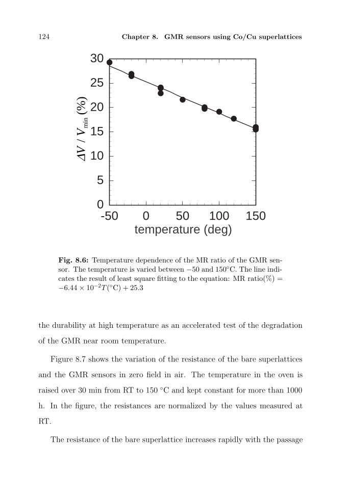
124 Chapter 8. GMR sensors using Co/Cu superlattices
0
5
10
15
20
25
30
-50 0 50 100 150temperature (deg)
∆V/ V
min
(%)
Fig. 8.6: Temperature dependence of the MR ratio of the GMR sen-sor. The temperature is varied between −50 and 150C. The line indi-cates the result of least square fitting to the equation: MR ratio(%) =−6.44 × 10⁻²T (C) + 25.3
the durability at high temperature as an accelerated test of the degradation
of the GMR near room temperature.
Figure 8.7 shows the variation of the resistance of the bare superlattices
and the GMR sensors in zero field in air. The temperature in the oven is
raised over 30 min from RT to 150 C and kept constant for more than 1000
h. In the figure, the resistances are normalized by the values measured at
RT.
The resistance of the bare superlattice increases rapidly with the passage

8.3. Results and discussion 125
0.5
1.0
1.5
2.0
2.5
3.0
0.1 1 10 100 1000
normalized resistance
time (hour)
150 °C
bare Co/Cu (superlattice)
passivated Co/Cu (sensor)
Fig. 8.7: Variation of the resistance of bare superlattices (dashedline) and sensors (solid line) during the durability test at 150 C inair. After passage of about 500 h, we checked the MR properties ofthe sensor by using the permanent magnet. Since the magnetizationprocess is irreversible, the step-like changes in the resistance are foundat 500 h and are not due to degradation of the sensors.
of time and dose not saturate until 20 h. The resistance at 20 h is 22.2 times
larger than the initial value (not plotted in Fig. 8.7). It is difficult to con-
tinue the durability test because of the degradation of the electrical contact
between the superlattices and the probe. Thus the durability test for the
bare superlattice is terminated at 20 h and the MR properties are measured
in the static field at RT. The resistance after the durability test does not
revert to the initial value and stays at a value of 18.7 times larger. The MR
ratio decreases to less than 0.8%. These significant changes in the MR prop-
erties are attributed to the oxidation of the Co/Cu superlattice. Therefore,
we must take care not to expose the superlattices to high temperature air
during the fabrication and use of GMR sensors.

126 Chapter 8. GMR sensors using Co/Cu superlattices
For the GMR sensors, the increase in resistance is confined in the first
30 min. After the passage of about 500 h, we checked the MR properties of
the GMR sensors by using the permanent magnet. Since the magnetization
process is irreversible, step-like changes in the resistance occur at 500 h and
are not due to the degradation of the sensor. Please note the slope of the
change in the resistance. Clearly, the resistance is very stable for more than
1000 h. Since the increase in the resistance up to first 30 min is due to the
intrinsic temperature dependence of the resistance of the Co/Cu superlattice,
the resistance measured after the durability test reverts to a value close to
the initial resistance. The difference between Rs measured before and after
the durability test is only −2.2% of the initial resistance. The MR curve
measured at room temperature after the durability test is shown in Fig 8.3(c).
The GMR sensors keep their MR ratio of 24.2% and their Hs of 500 Oe even
after the durability test. Although the MR properties change slightly after
the durability test, this will not cause significant problems in practical use.
This divests us of the prejudice that GMR sensors must be used only in
moderate conditions and extends the field of application of GMR sensors.
8.4 Conclusion
We have investigated the GMR in Co/Cu superlattices for the purpose of
practical application to magnetic sensors. We find that the superlattices
with the structure substrate/NiFe(5.0 nm)/Cu(2.1 nm)/[Co(1.0 nm)/Cu(2.1
nm)/]16 shows useful GMR properties.
Using this superlattices, we have fabricated GMR sensors and demon-
strated their performance as magnetic rotation sensors. In the appropriate

References 127
configuration of the sensor chip and the magnet rotor, the sensor output
changes more than 20%, synchronizing the rotation of the magnet, and is
almost independent of the rotation speed up to 2000 rpm.
Since the GMR sensors are passivated from the air by an SiO2 layer, they
shows extremely high durability against high temperature air. Even after
the sensors are left in the air of 150 C for 1000 h, the MR ratio of more than
24% and Hs ≈ 500 Oe are available.
Consequently, GMR sensors using Co/Cu superlattice can be used as
magnetic sensors in automobiles and aircraft under severe conditions.
References
[1] M. N. Baibich, J. M. Broto, A. Fert, F. Nguyen Van Dau, F. Petroff, P.
Etienne, G. Creuzet, A. Friederich, and J. Chazelas, Phys. Rev. Lett.
61, 2472 (1988).
[2] S. S. P. Parkin, R. Bhadra, and K. P. Roche, Phys. Rev. Lett. 66, 2152
(1991).
[3] D. H. Mosca, F. Petroff, A. Fert, P. A. Schroeder, W. P. Pratt Jr., and
R. Laloee, J. Magn. Magn. Mater. 94, L1 (1991).
[4] B. Dieny, V. S. Speriosu, S. S. P. Parkin, B. A. Gurney, D. R. Wilhoit,
and D. Mauri, Phys. Rev. B 43, 1297 (1991).
[5] B. Dieny, V. S. Speriosu, S. Metin, S. S. P. Parkin, B. A. Gurney, P.
Baumgart, and D. R. Wilhoit, J. Appl. Phys. 69, 4774 (1991).

128 Chapter 8. GMR sensors using Co/Cu superlattices
[6] A. Chaiken, P. Lubitz, J. J. Krebs, G. A. Prinz, and M. Z. Harford,
Appl. Phys. Lett. 59, 240 (1991).
[7] A. Chaiken, P. Lubitz, J. J. Krebs, G. A. Prinz, and M. Z. Harford, J.
Appl. Phys. 70, 5864 (1991).
[8] M. J. Hall, B. J. Hickey, M. A. Howson, C. Hammond, M. J. Walker,
D. G. Wright, D. Greig, and N. Wiser, J. Phys. Condens. Mater. 4, L495
(1992).
[9] Y. Saito, K. Inomata, K. Yusu, A. Goto, and H. Yasuoka, Phys. Rev. B
52, 6500 (1995).
[10] M. Suzuki, Y. Taga, A. Goto, and H. Yasuoka, J. Magn. Magn. Mater.
126, 495 (1993).
[11] M. Suzuki and Y. Taga, J. Appl. Phys. 74, 4660 (1993).
[12] M. Suzuki, Y. Taga, A. Goto, and H. Yasuoka, Phys. Rev. B 50, 18580
(1994).
[13] M. Suzuki and Y. Taga, Phys. Rev. B 52, 361 (1995).

List of Publications
[1] M. Suzuki, Y. Taga, A. Goto, and H. Yasuoka, ‘The critical thickness
of Fe buffer layer in giant magnetoresistance of Co/Cu superlattices’, J.
Magn. Magn. Mater. 126, 495 (1993).
[2] M. Suzuki and Y. Taga, ‘Giant magnetoresistance in Co/Cu superlat-
tices with mixed interfaces’, J. Appl. Phys. 74, 4660 (1993).
[3] M. Suzuki, Y. Taga, A. Goto, and H. Yasuoka, ‘X-ray diffraction and
NMR study on the structure of Co/Cu superlattices with artificially mod-
ified interfaces’, Phys. Rev. B 50, 18580 (1994).
[4] M. Suzuki and Y. Taga, ‘Role of interfacial roughness in the giant mag-
netoresistance in Co/Cu superlattices’, Phys. Rev. B 52, 361 (1995).
[5] M. Suzuki and Y. Taga, ‘Influence of bound d-state on the magnetoresis-
tance in magnetic multilayers’, J. Phys. Condens. Mater. 7, 8497 (1995).
[6] M. Suzuki and Y. Taga, ‘Relationship between the interfacial roughness
and the giant magnetoresistance in Co/Cu superlattices’, R&D Review
of TOYOTA CRDL 31, 43 (1996).
[7] M. Suzuki, T. Ohwaki and Y. Taga, ‘Durable giant magnetoresistive
sensors using Co/Cu superlattices’, Thin Solid Films 304, 333 (1997).
129

130 List of Publications
[8] M. Takeda, K. Saito, Y. Endo, M. Suzuki and Y. Taga, ‘Polarized neu-
tron reflectivity measurements of Co/Cu multilayers’, KENS report XI,
141 (1997).
[9] M. Suzuki and Y. Taga,「薄膜磁気センサの一課題–界面構造とGMR–」
in 「薄膜作製応用ハンドブック」 (in Japanease), 1st ed., edited by
S. Gonda, Y. Taga, T. Tsukada, and T. Hirao (NTS, Tokyo, 1995),
Chap. 6, Sec. 3, p. 1065.
[10] M. Suzuki and Y. Taga, ‘Anisotropy in the optical absorption of Ag–
SiO2 thin films with oblique columnar structure’, J. Appl. Phys. 71,
2848 (1992).
[11] M. Suzuki and Y. Taga, ‘Optical anisotropy and columnar structure of
obliquely deposited thin films containing fine particles’, J. Non-Cryst.
Solids 150, 148 (1992).
[12] M. Suzuki and Y. Taga, ‘Anisotropy in the optical absorption of metal-
insulator obliquely deposited thin films –The application for an inorganic
polarizer’, R&D Review of TOYOTA CRDL 29, 35 (1994).
[13] M. Suzuki and Y. Taga, ‘Anisotropy in the optical absorption of Ag–SiO2
thin films with oblique columnar structure’ in Selected Papers on Linear
Optical Composite Materials, Vol. MS 120 of SPIE Milestone Series,
edited by A. Lakhtakia (SPIE Optical Engineering Press, Washington,
1996), Chap. Sec. 3, p. 669.

List of Publications 131
[14] M. Suzuki, 「光位相差板・偏光膜」 in 「薄膜作製応用ハンドブック」
(in Japanease), 1st ed., edited by S. Gonda, Y. Taga, T. Tsukada, and
T. Hirao (NTS, Tokyo, 1995), Chap. 9, Sec. 4, p. 1170.
[15] M. Suzuki, H. Kawauchi, K. Kimura, and M. Mannami, ‘Surface Struc-
ture of SnTe(001) and PbSe/SnTe(001) Studied by RBS/Channeling of
MeV He+ Ions’, Surface Sci. 204, 223 (1988).
[16] Y. Fujii, K. Kimura, M. Hasegawa, M. Suzuki, Y. Susuki, and M. Man-
nami, ‘Surface Channeling of MeV He+ Ions on a SnTe Single Crystal’,
Nucl. Instrum. Meth. B33, 405 (1988).
[17] M. Hasegawa, K. Kimura, Y. Fujii, M. Suzuki, Y. Susuki, and M. Man-
nami, ‘Secondary Electron Emission due to MeV Ions at Glancing In-
cidence Angles on Clean Single Crystal Surfaces’, Nucl. Instrum. Meth.
B33, 334 (1988).
[18] K. Kimura, M. Hasegawa, Y. Fujii, M. Suzuki, Y. Susuki, and M. Man-
nami, ‘Specular Reflection of Fast Ions at a Single Crystal Surface’,
Nucl. Instrum. Meth. B33, 358 (1988).
[19] Y. Kido and M. Suzuki, ‘Direct Formation of Ferromagnetic MnBi Lay-
ers with Perpendicular Magnetic Anisotropy by Ion Beam Mixing’, Ma-
terials Letters 7, 219 (1988).