microwave device term project
DESCRIPTION
Microwave Device Term Project. Metamorphic Hemt device 성능 최적화 & 연구방향 2004/ 6/ 22 Lee Kang Min School of Electrical Engineering and Computer Science Seoul National University, Korea. Content. 1. Overview of Metamorphic-HEMT. - Introduction of Metamorphic-HEMT. - PowerPoint PPT PresentationTRANSCRIPT

Millimeterwave Device and Circuit Lab. Millimeterwave Device and Circuit Lab.
Microwave Device Term Microwave Device Term ProjectProjectMicrowave Device Term Microwave Device Term ProjectProject
Metamorphic Hemt device Metamorphic Hemt device 성능 최적화 성능 최적화 & & 연구방향연구방향
2004/ 6/ 222004/ 6/ 22
Lee Kang MinLee Kang Min
School of Electrical Engineering and Computer Science School of Electrical Engineering and Computer Science
Seoul National University, KoreaSeoul National University, Korea

ContentContent
1. Overview of Metamorphic-HEMT. - Introduction of Metamorphic-HEMT. 2. Key issue for Good performance Metamorphic-HEMT. -Process part. -Material Growth part.
3.Overcome method each key issue. -Process part. -Material Growth part.
4.Conclusion. -future work.

1. Overview of Metamorphic-1. Overview of Metamorphic-HEMTHEMT
1.HEMT 1.HEMT 소자의 종류소자의 종류 ( ( 구조별 분류구조별 분류 )) 1) Lattice-matched HEMT1) Lattice-matched HEMT
-- 격자 상수가 비슷한 물질들의 이용한 격자 상수가 비슷한 물질들의 이용한 HEMT HEMT 구조구조 -Conventional AlGaAs/GaAs -Conventional AlGaAs/GaAs 구조구조 -ex) InP based HEMT: Al-ex) InP based HEMT: Al0.480.48InIn0.520.52As/InAs/In0.530.53GaGa0.470.47As/InP As/InP 구조구조
2) Pseudomorphic HEMT2) Pseudomorphic HEMT -- 격자 상수가 다른 물질을 채널에 얇게 기른 격자 상수가 다른 물질을 채널에 얇게 기른 HEMT HEMT 구조구조 -ex)AlGaAs/GaAs HEMT-ex)AlGaAs/GaAs HEMT 의 의 channelchannel 에 에 InGaAs InGaAs 물질을 사용물질을 사용
3) Metamorphic HEMT3) Metamorphic HEMT
- GaAs substrate + InP HEMT Epitaxy- GaAs substrate + InP HEMT Epitaxy 를 이용한 를 이용한 HEMT HEMT 구조구조 - Buffer - Buffer 사용 사용
Metamorphic
low cost Good performance
GaAs InP

1. Overview of Metamorphic-1. Overview of Metamorphic-HEMTHEMT2. 2. Introduction of Metamorphic-HEMTIntroduction of Metamorphic-HEMT ▶ ▶ AdvantageAdvantage
- low cost & large scale (using GaAs substrate)- low cost & large scale (using GaAs substrate) - Multi-used. ( flexible Epitaxy design )- Multi-used. ( flexible Epitaxy design ) Low noise amp , power amp , switch ….Low noise amp , power amp , switch …. - Stable High frequency & low noise performance- Stable High frequency & low noise performance
▶ ▶ Disadvantage Disadvantage - Buffer issue-lattices mismatching - Buffer issue-lattices mismatching defect (Metamorphic defect (Metamorphic buffer) buffer)

2. Key issue for Good 2. Key issue for Good performance Metamorphic-performance Metamorphic-HEMTHEMT
Channel
SiNPassivation
x
Gate
SiN x
SideRecess
EHPGeneration
Cg,ext
Cg,ext
Lg
Dg
General process issue
• Lg Keeping (Lg/Dg)
• Suppression of Cg,ext.
• Surface Passivation.
• Gate, Ohmic metal tech.
5. Side Recess tech ( Breakdown voltage)
1.Process part

2. Key issue for Good 2. Key issue for Good performance Metamorphic-performance Metamorphic-HEMTHEMT
2.Material Growth part (Epitaxy design)
General Material issue
• Use of suitable InGaAs Channel
• Use of suitable M-buffer layer (Epi growth)
& Doping profile
InAlAs Barrier
InGaAs Channel
InAlAs buffer
Metamorphic-buffer
Si delta doping
InGaAs cap
Gate
Source Drain
GaAs Substrate

3.Overcome method each key 3.Overcome method each key issueissue
1.Process 1.Process partpart 1) Lg 1) Lg Keeping (Lg/Dg) Keeping (Lg/Dg) - Cappy group 2002. EL ( Lg=60nm ) - Cappy group 2002. EL ( Lg=60nm )
DC: Gm= 850mS/mm , Ids~600mA/mmRF: Ft=260GHz , Fmax=490GHz
* General Lg=0.1um Ft>200GHz (In0.53Ga0.48As channel using )
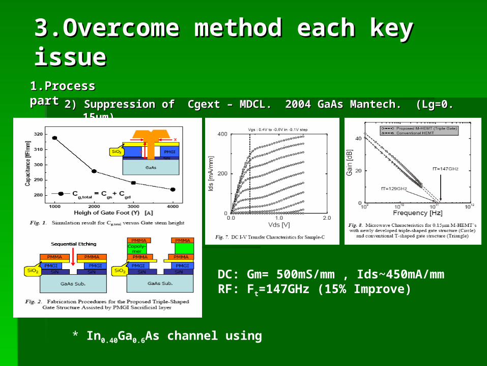
3.Overcome method each key 3.Overcome method each key issueissue
1.Process 1.Process partpart 2) Suppression of Cgext – MDCL. 2004 GaAs Mantech.2) Suppression of Cgext – MDCL. 2004 GaAs Mantech. (Lg=0.15um)(Lg=0.15um)
DC: Gm= 500mS/mm , Ids~450mA/mmRF: Ft=147GHz (15% Improve)
* In0.40Ga0.6As channel using

3.Overcome method each key 3.Overcome method each key issueissue
-2.0 -1.5 -1.0 -0.5 0.0 0.5 1.00
200
400
600
0
200
400
600
I DS[m
A/m
m]
VGS
[V]
Before passivation After passibation
VDS
=1,1.25 V
Gm
[mS
/mm
]
1.Process 1.Process partpart 3) Surface passivation – MDCL. Experiment (Lg=0.1um)3) Surface passivation – MDCL. Experiment (Lg=0.1um)
DC: Gm= 590mS/mm(~20% improve) , Ids=600mA/mm
* In0.35Ga0.65As channel using
0 1 20
200
400
600
VGS
=-2 to 0.7 in 0.3V step
I DS[m
A/m
m]
VDS
[V]
Before passivation After passivation

3.Overcome method each key 3.Overcome method each key issueissue1.Process 1.Process partpart 4) Gate, Ohmic metal tech – Jantz group, GaAs reilability symposium 2001 (lg=0.14) Gate, Ohmic metal tech – Jantz group, GaAs reilability symposium 2001 (lg=0.1
2um)2um)
Ti Oxidation , Pt buried gate – better reilabilty & device performance
* In0.3Ga0.7As channel using

3.Overcome method each key 3.Overcome method each key issueissue1.Process 1.Process partpart 4) Gate, Ohmic metal tech – MDCL experiment ,4) Gate, Ohmic metal tech – MDCL experiment ,
* In0.35Ga0.65As channel using : Rc= 0.13
General using : Rc= 0.15 (cappy group) Rc≥0.15
*) Reliability of metamorphic HEMTs on GaAs substrates,Reliability of metamorphic HEMTs on GaAs substrates, RaytRaytheon GaAs reilability symposium 2001heon GaAs reilability symposium 2001
Pd ohmic Pd ohmic
320 330 340 350 3600.10
0.15
0.20
0.25
0.30
0.35
Rc[o
hm.m
m]
Alloy Temperature
Ni/Ge/Au=100/450/2000 Ni/Ge/Au=200/800/2000 Ni/Ge/Au=150/800/2000

3.Overcome method each key 3.Overcome method each key issueissue1.Process 1.Process partpart 5) Side Recess tech- K.C Hwang group , IEEE MGWL 1998 (Lg=0.1um)(Lg=0.1um)
Double Recess ,Double DopedDouble Recess ,Double DopedGm : 1050 mS/mmGm : 1050 mS/mmCurrent density : 750mA/mmCurrent density : 750mA/mmBVgd: 8.3V Power sensity: 509mW/mmBVgd: 8.3V Power sensity: 509mW/mm ( InP-645mW/mm)( InP-645mW/mm)
최적의 전력 성능 – 높은 출력 최적의 전력 성능 – 높은 출력 current, current, 높은 높은 breakdown breakdown 전압전압Epi- Drain Epi- Drain 부근의 부근의 InGaAs channel InGaAs channel 에서 최대 전계 감소시키는 구조에서 최대 전계 감소시키는 구조Double-doped process Double-doped process 구조 구조 - drain - drain 전류 전류 breakdown breakdown 전압 최적화전압 최적화
* In0.65Ga0.35As channel using
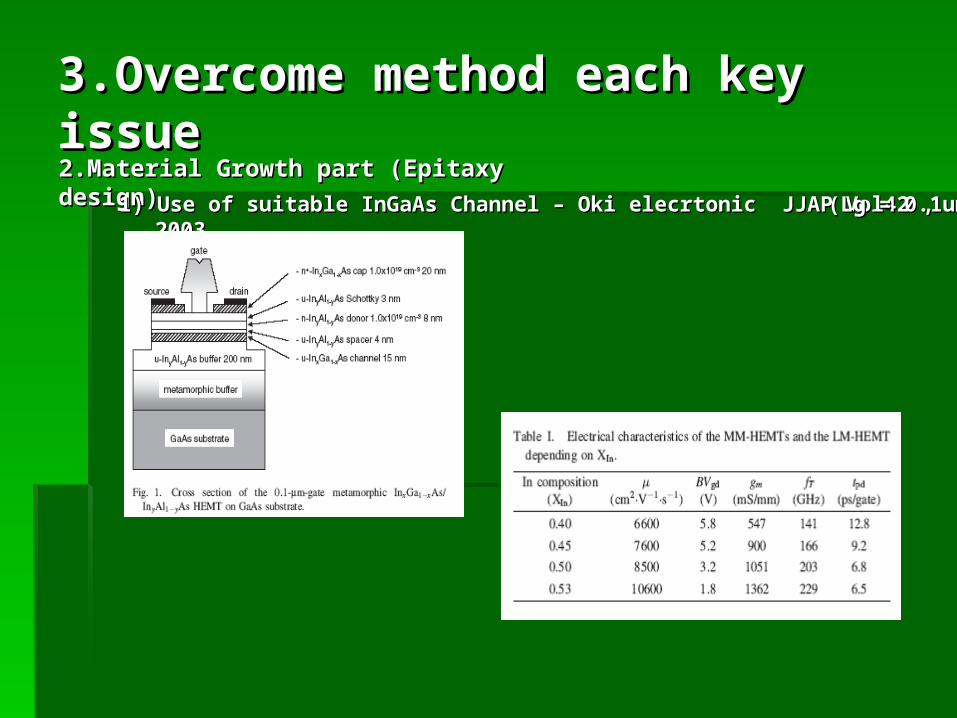
3.Overcome method each key 3.Overcome method each key issueissue2.Material Growth part (Epitaxy design)2.Material Growth part (Epitaxy design)
1) Use of suitable InGaAs Channel – Oki elecrtonic JJAP Vol42 ,20031) Use of suitable InGaAs Channel – Oki elecrtonic JJAP Vol42 ,2003 (Lg = 0.1um)(Lg = 0.1um)

3.Overcome method each key 3.Overcome method each key issueissue2.Material Growth part (Epitaxy design)2.Material Growth part (Epitaxy design)
1) Use of suitable InGaAs Channel – Weimen group EDL 1996 (0.13um) 1) Use of suitable InGaAs Channel – Weimen group EDL 1996 (0.13um)
Composit channel (for kink free)Composit channel (for kink free)InIn0.520.52AlAl0.480.48As : transport As : transport 특성이 우수함특성이 우수함 ..
InIn0.320.32GaGa0.680.68As : impact ionization As : impact ionization 특성이 낮아서 특성이 낮아서 좋음좋음 .. 두 물질을 섞어서 사용하여 두 물질을 섞어서 사용하여 DC DC 특성 및 특성 및 impact ionization impact ionization 특성이 우수한 특성이 우수한 mHEMT mHEMT 소자 구현소자 구현
Output conductance : 20 mS/mmOutput conductance : 20 mS/mm
Maximum drain current : 750 mA/mmMaximum drain current : 750 mA/mm
Ft= 160GHz ,Fmax= 350GHzFt= 160GHz ,Fmax= 350GHz

3.Overcome method each key 3.Overcome method each key issueissue2.Material Growth part (Epitaxy design)2.Material Growth part (Epitaxy design)
2) 2) Use of suitable M-buffer layer (Epi growth) –G.Borghs group, 1999 GaAs MantechUse of suitable M-buffer layer (Epi growth) –G.Borghs group, 1999 GaAs Mantech
1> ternary buffer (InAlAs)1> ternary buffer (InAlAs) – General gradingGeneral grading2> quaternary buffer (AlGaAsSb)- Top of buffer ( lattice-matching InAlAs )2> quaternary buffer (AlGaAsSb)- Top of buffer ( lattice-matching InAlAs ) - low defect density- low defect density
quaternary buffer (AlGaAsSb)quaternary buffer (AlGaAsSb)Gm=800ms/mm, Ids~500mAGm=800ms/mm, Ids~500mA Ft=87GHz Fmax=140GHzFt=87GHz Fmax=140GHz
ternary buffer (InAlAs)ternary buffer (InAlAs)Gm=860ms/mm, Ids~450mAGm=860ms/mm, Ids~450mA Ft=75GHz Fmax=115GHzFt=75GHz Fmax=115GHz
4.Conclusion4.Conclusion
1. 경제적인 소자
2. 목적에 따른 소자 연구가능 & application 다양 (high speed MHEMT, power MHEMT, ..) Power HEMT 에 집중하는 것이 효과적 .
3. Process- 고려 해야 할 변수가 많다 . 기준에 따른 최적화 (trade off) (Idss & BVgd , ..) 4. Epitaxy- 최적화를 위한 Epi design (buffer, channel ,Ns..)
ReferanceReferance
1. 0.13 μm gate-length In0.52Al0.48As-In0.53Ga0.47 As metamorphic HEMTs on GaAs substrate- Dumka, D.C ,Device Research Conference, 2000. Conference Digest2. 0.1um gate metamorphic HEMT on GaAs and its application to SCFL- Tomoyuki . JJAP 20033. Reliability of metamorphic HEMTs on GaAs substrates-Marsh, P.F , GaAs Reliability Workshop, 20014. Status of metamorphic InxAl1-xAs/Inx Ga1-xAs HEMTs- cappy A , Gallium Arsenide Integrated Circuit (GaAs IC) Symposium, 1999 5. Metamorphic InAlAs/InGaAs HEMTs on GaAs substrates with a novel composite channels design
Chertouk, M. Electron Device Letters 19966. Fmax of 490 GHz metamorphic In0.52Al0.48 As/In0.53Ga0.47As HEMTs on GaAs substrate- Cappy A . Electronics Letters 20027. Properties of metamorphic materials and device structures on GaAs substrates- Hsieh, K.C Molecular Beam Epitaxy International Conference 20028. Effect of gate metal on reliability of metamorphic HEMTs- Jantz, W GaAs Reliability Workshop, 20019. Metamorphic InAlAs/InGaAs HEMT on GaAs substrate with a novel composite channel design Weimann , Electronics Device Letters 199610. 0.15µm In0.4GaAs/In0.4AlAs Metamorphic HEMT’s (M-HEMT’s) Using A Novel Triple Shaped Gate Structure Assisted By PMGI Resist- Kim . GaAs Mantach 2004…..