miniature sensor node with conformal phased array
TRANSCRIPT
752 G. A. E. VANDENBOSCH, ET AL., MINIATURE SENSOR NODE WITH CONFORMAL PHASED ARRAY
Miniature Sensor Node with Conformal Phased Array
Guy A. E. VANDENBOSCH1, Alexander VASYLCHENKO1,2, Montserrat FERNANDEZ-BOLANOS3, Steven BREBELS2, Walter DE RAEDT2, Adrian Mihai IONESCU3
1 Dept. of Electrical Engineering, Katholieke Universiteit Leuven, Kasteelpark Arenberg 10, 3001 Leuven, Belgium 2 RF-CDM group, IMEC, Kapeldreef 75, 3001 Leuven, Belgium
3 Nanoelectronic Device Laboratory, École Polytechnique Férérale de Lausanne, 1015 Lausanne, Switzerland
Abstract. This paper reports on the design and fabrication of a fully integrated antenna beam steering concept for wireless sensor nodes. The conformal array circumcises four cube faces with a silicon core mounted on each face. Every silicon core represents a 2 by 1 antenna array with an antenna element consisting of a dipole antenna, a balun, and a distributed MEMS phase shifter. All these components are based on a single wafer process and designed to work at 17.2 GHz. Simulations of the entire system and first results of individual devices are reported.
Keywords Conformal array, sensor node, miniaturization.
1. Introduction Many vital parameters of airborne systems require
a continuous monitoring of signals coming from sensors placed all over an aircraft. Wireless sensor nodes allow building a flexible network of various sensors, communi-cating with each other and/or with a central control system, while omitting heavy wiring to a cabin computer (Fig. 1). A sensor node utilizing an adaptive steerable antenna array enables electronically controlled network reconfigurability. This can be done by reorganizing the connections through redirection of the antenna beam. This may greatly improve the reliability of the whole sensor network. Indeed a sensor node consists of different functional layers such as a radio system, a processing unit, a sensor, a power storage unit and possibly even an energy scavenging system. We pro-pose a conceptual RF radio subsystem for an ultra small sensor cube with dimensions of 1 cm3, which is based on a combination of system-on-chip (SoC) solutions.
Although it is a standard approach for traditionally sized beam steered arrays [1], using discrete components such as a feeding network, phase shifters, and antennas is inapplicable for building an efficient and yet very small phased array. Moreover, although several technologies are available to fabricate antennas [2], [3], integrating all these
components on the same substrate allows miniaturizing the system, avoiding extra losses and high packaging cost.
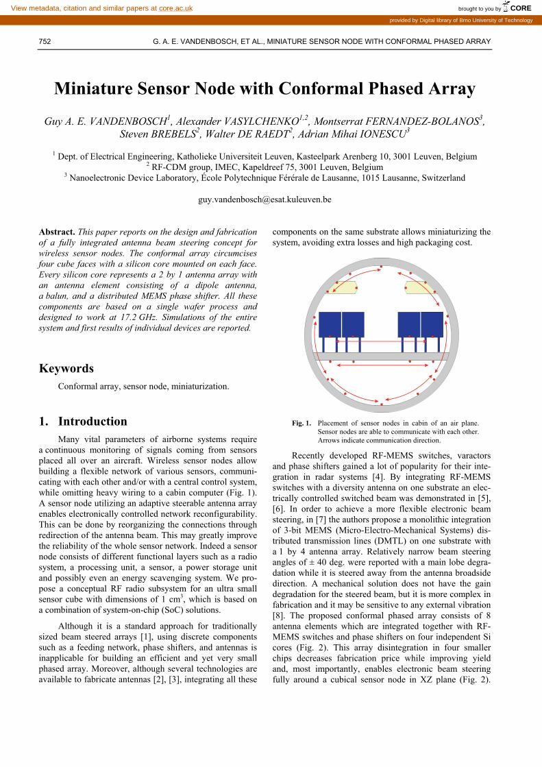
Fig. 1. Placement of sensor nodes in cabin of an air plane.
Sensor nodes are able to communicate with each other. Arrows indicate communication direction.
Recently developed RF-MEMS switches, varactors and phase shifters gained a lot of popularity for their inte-gration in radar systems [4]. By integrating RF-MEMS switches with a diversity antenna on one substrate an elec-trically controlled switched beam was demonstrated in [5], [6]. In order to achieve a more flexible electronic beam steering, in [7] the authors propose a monolithic integration of 3-bit MEMS (Micro-Electro-Mechanical Systems) dis-tributed transmission lines (DMTL) on one substrate with a 1 by 4 antenna array. Relatively narrow beam steering angles of ± 40 deg. were reported with a main lobe degra-dation while it is steered away from the antenna broadside direction. A mechanical solution does not have the gain degradation for the steered beam, but it is more complex in fabrication and it may be sensitive to any external vibration [8]. The proposed conformal phased array consists of 8 antenna elements which are integrated together with RF-MEMS switches and phase shifters on four independent Si cores (Fig. 2). This array disintegration in four smaller chips decreases fabrication price while improving yield and, most importantly, enables electronic beam steering fully around a cubical sensor node in XZ plane (Fig. 2).
brought to you by COREView metadata, citation and similar papers at core.ac.uk
provided by Digital library of Brno University of Technology
RADIOENGINEERING, VOL. 20, NO. 4, DECEMBER 2011 753
Detailed information on the realization of the cubical antenna topology can be found in [9].
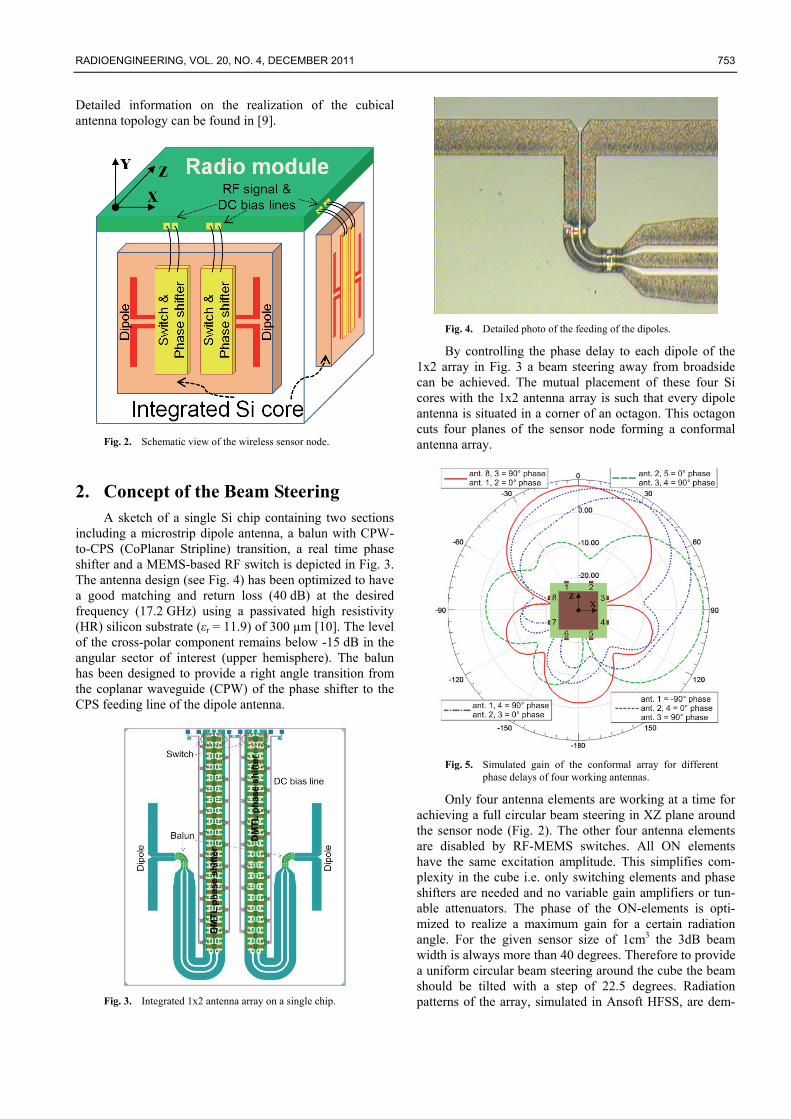
Fig. 2. Schematic view of the wireless sensor node.
2. Concept of the Beam Steering A sketch of a single Si chip containing two sections
including a microstrip dipole antenna, a balun with CPW-to-CPS (CoPlanar Stripline) transition, a real time phase shifter and a MEMS-based RF switch is depicted in Fig. 3. The antenna design (see Fig. 4) has been optimized to have a good matching and return loss (40 dB) at the desired frequency (17.2 GHz) using a passivated high resistivity (HR) silicon substrate (εr = 11.9) of 300 µm [10]. The level of the cross-polar component remains below -15 dB in the angular sector of interest (upper hemisphere). The balun has been designed to provide a right angle transition from the coplanar waveguide (CPW) of the phase shifter to the CPS feeding line of the dipole antenna.
Fig. 3. Integrated 1x2 antenna array on a single chip.
Fig. 4. Detailed photo of the feeding of the dipoles.
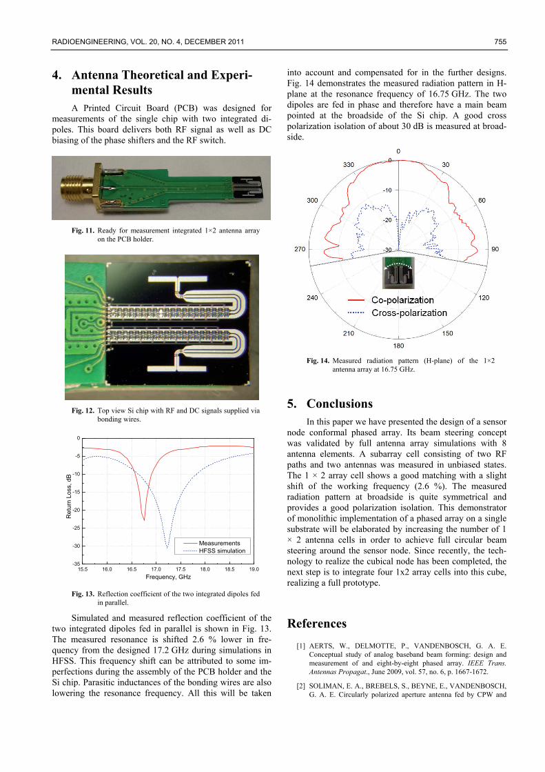
By controlling the phase delay to each dipole of the 1x2 array in Fig. 3 a beam steering away from broadside can be achieved. The mutual placement of these four Si cores with the 1x2 antenna array is such that every dipole antenna is situated in a corner of an octagon. This octagon cuts four planes of the sensor node forming a conformal antenna array.
Fig. 5. Simulated gain of the conformal array for different
phase delays of four working antennas.
Only four antenna elements are working at a time for achieving a full circular beam steering in XZ plane around the sensor node (Fig. 2). The other four antenna elements are disabled by RF-MEMS switches. All ON elements have the same excitation amplitude. This simplifies com-plexity in the cube i.e. only switching elements and phase shifters are needed and no variable gain amplifiers or tun-able attenuators. The phase of the ON-elements is opti-mized to realize a maximum gain for a certain radiation angle. For the given sensor size of 1cm3 the 3dB beam width is always more than 40 degrees. Therefore to provide a uniform circular beam steering around the cube the beam should be tilted with a step of 22.5 degrees. Radiation patterns of the array, simulated in Ansoft HFSS, are dem-
754 G. A. E. VANDENBOSCH, ET AL., MINIATURE SENSOR NODE WITH CONFORMAL PHASED ARRAY
onstrated in Fig. 5. The gain of the steered beam remains constant within a level of 8.2-8.5 dBi.
3. Monolithic Integration of the Phase Shifter and Its Performance The phase shifter is realized using a DMTL digital
approach which consists of a CPW periodically loaded by capacitive MEMS switches. The whole system is fabricated using a 10 kΩcm P-type HR Si substrate.
Fig. 6. Top view of the DMTL loaded in a CPW.
0 0.5 1 1.5 2 2.5 3 3.5 4
x 1010
-1400
-1200
-1000
-800
-600
-400
-200
0
Pha
se S
21 [
°]
Frequency, GHz
Fig. 7. Measured S21 argument in different bias states.
A seven-mask process described in [11] in detail is used. CPWs and the dipole antenna are made of sputtered 3 µm Al. Al also acts as structural material to anchor the suspended MEMS and air bridges of the balun and the phase shifter (Fig. 6). The top movable electrode is com-posed of a thin sputtered Al (1.5 µm) and thick electro-plated nickel (Ni) (5 µm) is used for the anchoring, the non-movable air bridges, and the stiff bars to avoid defor-mation of the thin membrane.
Initially a standalone phase shifter was characterized and measured. The pull-in voltage of all the switches of the DMTL starts at about 17 V bias voltage.
0.5 1 1.5 2 2.5 3 3.5 4
x 1010
-50
-40
-30
-20
-10
0
S11
[dB
]
Frequency, GHz
A/B bits biasing 0V / 0VA/B bits biasing 20V / 0VA/B bits biasing 0V / 20VA/B bits biasing 20V / 20V
Fig. 8. Measured reflection coefficient of the phase shifter in
different bias states.
0.5 1 1.5 2 2.5 3 3.5 4
x 1010
-10
-8
-6
-4
-2
0
S21
[dB
]
Frequency, GHz
Fig. 9. Measured pass loss of the phase shifter in different bias states.
0 0.5 1 1.5 2 2.5 3 3.5 4
x 1010
-12
-10
-8
-6
-4
-2
0
Loss
[dB
]
Frequency, GHz
A/B bits biasing 0V / 0VA/B bits biasing 20V / 0VA/B bits biasing 0V / 20VA/B bits biasing 20V / 20V
Fig. 10. Measured losses of the phase shifter in different bias
states.
Fig. 7 shows the phase delay provided by a DMTL for various bits activation. The measured S11 and S21 are presented in Fig. 8 and Fig. 9 respectively. The total losses in the phase shifter in the Up and Down states are measured to be 3 dB and 5 dB (Fig. 10), which comes to 4.9 dB/mm and 0.82 dB/mm losses respectively.
RADIOENGINEERING, VOL. 20, NO. 4, DECEMBER 2011 755
4. Antenna Theoretical and Experi-mental Results A Printed Circuit Board (PCB) was designed for
measurements of the single chip with two integrated di-poles. This board delivers both RF signal as well as DC biasing of the phase shifters and the RF switch.
Fig. 11. Ready for measurement integrated 1×2 antenna array
on the PCB holder.
Fig. 12. Top view Si chip with RF and DC signals supplied via
bonding wires.
Fig. 13. Reflection coefficient of the two integrated dipoles fed
in parallel.
Simulated and measured reflection coefficient of the two integrated dipoles fed in parallel is shown in Fig. 13. The measured resonance is shifted 2.6 % lower in fre-quency from the designed 17.2 GHz during simulations in HFSS. This frequency shift can be attributed to some im-perfections during the assembly of the PCB holder and the Si chip. Parasitic inductances of the bonding wires are also lowering the resonance frequency. All this will be taken
into account and compensated for in the further designs. Fig. 14 demonstrates the measured radiation pattern in H-plane at the resonance frequency of 16.75 GHz. The two dipoles are fed in phase and therefore have a main beam pointed at the broadside of the Si chip. A good cross polarization isolation of about 30 dB is measured at broad-side.
Fig. 14. Measured radiation pattern (H-plane) of the 1×2 antenna array at 16.75 GHz.
5. Conclusions In this paper we have presented the design of a sensor
node conformal phased array. Its beam steering concept was validated by full antenna array simulations with 8 antenna elements. A subarray cell consisting of two RF paths and two antennas was measured in unbiased states. The 1 × 2 array cell shows a good matching with a slight shift of the working frequency (2.6 %). The measured radiation pattern at broadside is quite symmetrical and provides a good polarization isolation. This demonstrator of monolithic implementation of a phased array on a single substrate will be elaborated by increasing the number of 1 × 2 antenna cells in order to achieve full circular beam steering around the sensor node. Since recently, the tech-nology to realize the cubical node has been completed, the next step is to integrate four 1x2 array cells into this cube, realizing a full prototype.
References
[1] AERTS, W., DELMOTTE, P., VANDENBOSCH, G. A. E. Conceptual study of analog baseband beam forming: design and measurement of and eight-by-eight phased array. IEEE Trans. Antennas Propagat., June 2009, vol. 57, no. 6, p. 1667-1672.
[2] SOLIMAN, E. A., BREBELS, S., BEYNE, E., VANDENBOSCH, G. A. E. Circularly polarized aperture antenna fed by CPW and
756 G. A. E. VANDENBOSCH, ET AL., MINIATURE SENSOR NODE WITH CONFORMAL PHASED ARRAY
built in MCM-D technology. Electron. Lett., Feb. 1999, vol. 35, no. 4, pp. 250-251.
[3] SOLIMAN, E. A., BREBELS, S., BEYNE, E., VANDENBOSCH, G. A. E. CPW fed cusp antenna. Microwave and Opt. Techn. Lett., Aug. 1999, vol. 22, no. 4, p. 288-290.
[4] VAN CAEKENBERGHE, K. RF MEMS on the Radar. IEEE Microwave Mag., October 2009, vol. 10, p. 99-116.
[5] CETINER, B. A., QIAN, J. Y., CHANG, H. P., BACHMAN, M., LI, G. P., DE FLAVIIS, F. Monolithic integration of RF MEMS switches with a diversity antenna on PCB substrate. IEEE Trans. Microw. Theory Tech., January 2003, vol. 51, no. 1, p. 332-335.
[6] CHENG, S., RANTAKARI, P., MALMQVIST, R., SAMUELSSON, C., VÄHÄ-HEIKKILÄ, T., RYDBERG, A., VARIS, J. Switched beam antenna based on RF MEMS SPDT switch on quartz substrate. IEEE Antennas Wireless Propag. Lett., 2009, vol. 8, p. 383-386.
[7] TOPALLI, K., CIVI, Ö. A., DEMIR, S., KOC, S., AKIN, T. A monolithic phased array using 3-bit distributed RF MEMS phase shifters. IEEE Trans. Microw. Theory Tech., February 2008, vol. 56, no. 2, p. 270-277.
[8] BAEK, C.-W., SONG, S., PARK, J.-H., LEE, S., KIM, J.-M., CHOI, W., CHEON, C., KIM, Y.-K., KWON, Y. A V-band micromachined 2-D beam-steering antenna driven be magnetic force with polymer-based hinges. IEEE Trans. Microw. Theory Tech., January 2003, vol. 51, no. 1, p. 325-331.
[9] ENAYATI, A., BREBELS, S., DE RAEDT, W., VANDENBOSCH, G. A. E. 3D-antenna-in-package solution for microwave wireless sensor network nodes. IEEE Trans. Antennas Propagat., Oct. 2011, vol. 59, no. 10, p. 3617-3623.
[10] FERNÁNDEZ-BOLAÑOS, M., VASYLCHENKO, A., DAINESI, P., BREBELS, S., DE RAEDT, W., VANDENBOSCH, G. A. E., IONESCU, A. M. Dipole antenna and distributed MEMS phase shifter fully integrated in a single wafer process for beam steering applications. Microelectron. Eng., Feb. 2010, vol. 87, p. 1290-1293.
[11] FERNÁNDEZ-BOLAÑOS, M., PERRUISSEAU-CARRIER, J., DAINESI, P., IONESCU, A. M. RF MEMS capacitive switch on semi-suspended CPW using low-loss high-resistivity silicon substrate. Microelec. Eng., June 2007, vol. 85, p. 1039-1042.
About Authors ... Guy A. E. VANDENBOSCH was born in Sint-Niklaas, Belgium, on May 4, 1962. He received the M.S. and Ph.D. degrees in Electrical Engineering from the Katholieke Universiteit Leuven, Leuven, Belgium, in 1985 and 1991, respectively. Since 1993, he has been a Lecturer, and since 2005, a Full Professor at the same university. His research interests are in the area of electromagnetic theory, compu-tational electromagnetics, planar antennas and circuits, electromagnetic radiation, electromagnetic compatibility, and bio-electromagnetics. Guy Vandenbosch has been a member of the “Management Committees” of the con-secutive European COST actions on antennas since 1993, where he is leading the working group on modeling and software for antennas. Within the ACE Network of Excel-lence of the EU (2004-2007), he was a member of the Executive Board and coordinated the activity on the crea-tion of a European antenna software platform. Currently he
is also the chair person of the IEEE-AP/MTT Benelux section.
Alexander VASYLCHENKO received the M.Sc. degree in Radiophysics and the M.Sc. degree in CS from Kharkiv National University and National University of Radio Electronics (Ukraine) in 2000 and 2002. He received his Ph.D. degree in Electrical Engineering from the Katholieke Universiteit Leuven in Belgium in 2010. From 2005 till 2010, he was a contributor to the Antenna Software Initia-tive within the ACE Network of Excellence of the EU, where he has been participating in the Antenna Software Benchmark Activity for Challenging Applications. He is currently working at CSEM (Switzerland) on development of antenna systems. His work involves development of miniature antennas and integration in SiP/SoC wireless modules, antennas for BAN and medical applications with a strong focus on propagation phenomena.
Montserrat FERNANDEZ-BOLANOS BADIA received the M.Sc. degree in Telecommunication Engineering from the University of Seville, Spain, in 2005. She received her Ph.D degree in Microsystems and Microelectronics from Ecole Polytechnique Fédérale de Lausanne (EPFL) in 2010. Since August 2010, she works as scientific collabo-rator in the Nanoelectronic device laboratory (NANOLAB) at EPFL. The focus of her research is in the field of RF MEMS switches, phase shifters, and tunable filters for airborne and space applications. Her present research inter-ests include the open challenges of RF MEMS devices such as reliability, packaging and their 3D integration with RF ICs.
Steven BREBELS received the M.S. degree in Electrical Engineering from the University of Leuven, Belgium, and is currently working toward the Ph.D. degree at the Inter-university Microelectronics Center (IMEC), Leuven, Bel-gium. His research within the RF Component Design and Modeling group, IMEC, is directed to integrated circuits and antennas in thin-film and 3D stacked modules. His research interests include microwave and millimeter-wave components and integrated antennas. Steven Brebels is co-recipient of the IEEE 2003 Microwave Prize. The paper detailed the "Accurate Modeling of High-Q Spiral Induc-tors in Thin-Film Multilayer Technology for Wireless Telecommunication Applications."
Walter DE RAEDT graduated in Electrical Engineering (1981) at KU Leuven, Belgium. From 1981 until 1984 his research focused on ebeam technology at KU Leuven labs. In 1984 he joined IMEC at its start as a project leader in charge of submicron technologies for advanced HEMT devices until 1997. In 1987 he was visiting scientist at IBM Rüschlikon working on fast III-V circuits. From 1997, he joined the MCM group at IMEC in charge of the design, modeling and characterization activities for packaging. Currently he is head of the RFCDM group at IMEC and was involved in many EU research projects (MIPA, 3DµTune, Shift, e-cubes…). In 2003 he received the IEEE microwave prize with his team. He authored and co-

RADIOENGINEERING, VOL. 20, NO. 4, DECEMBER 2011 757
authored more than 200 papers, several patents and book chapters in the field of microwave/mmwave modeling, design and packaging. His current interests are in the field of MEMS-based solutions and SiP (System in package) integration for wireless systems.
Adrian Mihai IONESCU is an Associate Professor at the Swiss Federal Institute of Technology, Lausanne, Switzer-land. He received the B.S./M.S. and Ph.D. degrees from the Polytechnic Institute of Bucharest, Romania and the National Polytechnic Institute of Grenoble, France, in 1989 and 1997, respectively. He has held staff and/or visiting positions at LETI-CEA, Grenoble, France, LPCS-
ENSERG, Grenoble, France and Stanford University, USA, during 1998 and 1999. His research interests focus on micro- and nano-electronic devices aimed at Integrated Circuit design, especially process development, modeling and electrical characterization. Dr. Ionescu has published more than 250 articles in international journals and conferences. He received three Best Paper Awards in international conferences and the Annual Award of the Technical Section of the Romanian Academy (of Sciences) in 1994. He is director of the Laboratory of Micro/Nanoelectronic Devices (NANOLAB) and head of the Doctoral School in Microsystems and Microelectronics of EPFL.