optimus fabric interface specification - 京微雅格 - output 32 apb write data bus pwrite output 1...
TRANSCRIPT
AHB2APB Bridge
User Guide
11/2013
Capital Microelectronics, Inc.
China
User Guide of AHB2APB Bridge
http://www.capital-micro.com 2
Contents
Contents ............................................................................................................................................... 2
1 Introduction ................................................................................................................................... 3
2 AHB2APB Bridge Overview......................................................................................................... 4
2.1 Pin Description ........................................................................................................................ 4
2.2 Parameter Description ............................................................................................................ 4
2.3 Block Diagram ......................................................................................................................... 5
3 AHB2APB Bridge IP Usage ......................................................................................................... 6
3.1 AHB2APB Bridge operation timing diagram ........................................................................... 6
3.2 AHB2APB Bridge address mapping ...................................................................................... 11
4 Resource usage and performance analysis ............................................................................ 12
5 Generate File Directory Structure ............................................................................................. 13
Revision History ................................................................................................................................ 15

User Guide of AHB2APB Bridge
http://www.capital-micro.com 3
1 Introduction
This document mainly describes the usage of the AHB2APB Bridge IP. It works as AHB bus slave and
APB bus master. So, if there is no APB bus provided, the APB slave blocks can be connected to AHB
masters through the AHB2APB Bridge.
The AHB2APB Bridge IP supports the following features:
Compliance with the AMBA Specification, Revision 2.0 from ARM
Single and burst AHB transfer
Up to 16 APB slaves, the slave number can be configured
32-bit AHB data buses
32-bit APB data buses
Little-endian AHB systems
Big-endian and little-endian APB systems
APB slave address space can be configured
- All slaves must have their address spaces aligned to a 1 K boundary.
- Minimum address space allocated to a configured slave is 1 K.
Synchronous hclk/pclk; hclk is an integer multiple of pclk
Device family support:
CME-M7A

User Guide of AHB2APB Bridge
http://www.capital-micro.com 4
2 AHB2APB Bridge Overview
2.1 Pin Description
Table 2-1 AHB2APB Bridge interface
Interface Name Direction Width Description
System hclk Input 1 AHB interface clock
hresetn Input 1 AHB interface reset, low active
AHB
interface
haddr Input 1 AHB address bus
hwrite Input 1 AHB transfer direction: 1-write,
0-read
hwdata Input 32 AHB write data bus
hrdata Output 32 AHB read data bus
hsel Input 1 AHB slave select signal
hready_resp Output 1 Transfer done output
hresp Output 1 Transfer response signal
htrans Input 2 AHB Transfer type signal
hsize Input 3 AHB Transfer size
hburst Input 3 AHB Transfer type signal
APB
interface
pclk_en Input 1 APB bus clock enable
paddr Output 32 APB address bus
pwdata Output 32 APB write data bus
pwrite Output 1 APB transfer direction: 1-write,
0-read
penable Output 1 Data valid strobe
psel_s0
~
psel_s15
Output 1 Peripheral select signal of APB
slave
Prdata_s0
~
prdata_s15
Input 32 APB read data bus
2.2 Parameter Description
Table 2-2 AHB2APB Bridge parameter description
Name Type Value Description

User Guide of AHB2APB Bridge
http://www.capital-micro.com 5
BIG_ENDIAN Integer 1/0 Big or little endian for APB system
NUM_APB_SLAVES Integer 1~16 Number of APB slave
START_PADDR_SN Integer
32’ha000_0000~
32’hbfff_fc00
or
32’hc000_0000~
32’hdfff_fc00
Start address of APB slave N, 1K
boundary in FP0/FP1 address space
END_PADDR_SN Integer
32’ha000_03ff~
32’hbfff_ffff
or
32’hc000_03ff~
32’hdfff_ffff
End address of APB slave N, 1K
boundary in FP0/FP1 address space
2.3 Block Diagram
AHB Slave
Interface
Address
Decoder
Read Data
Mux
AHB2APB Bridge
…
…
APB
Bus
signals…
…
AHB
Bus
signals
Figure 2-1 AHB2APB Bridge IP block diagram
AHB Slave Interface module transforms AHB bus signals into APB bus control signals and the
Address Decoder will decodes the address input and generates the select signals to select data form
Read Data MUX module.

User Guide of AHB2APB Bridge
http://www.capital-micro.com 6
3 AHB2APB Bridge IP Usage
3.1 AHB2APB Bridge operation timing diagram
1 2 3 4 5 6 7 8 9 10
addr1
2
data1
addr1
data1
TimeGen
pclk
hclk
pck_en
hsel
haddr
htrans
hwrite
hready_resp
hrdata
psel
paddr
penable
pwrite
prdata
Figure 3-1 Basic read transfer((pclk=hclk)
In the figure 3-1, it is described how to transform the AHB bus signals to APB bus signals in the basic
read transfer .The single transfer consists of one address cycle and one data cycle on the AHB bus
side.
If the pclk is equal to hclk, the transfer starts on the AHB first hclk rising edge and the address is
sampled by the APB Bridge on the next hclk rising edge. Then the address and hwrite signal are
broadcasted and the psel signal is generated and the penable signal is generated on the next hclk
rising edge. During the penbale valid, the prdata must be provided and routed directly back to the
AHB.

User Guide of AHB2APB Bridge
http://www.capital-micro.com 7
1 2 3 4 5 6 7 8 9 10 11 12 13 14
addr1
2
data1
addr1
data1
TimeGen
pclk
hclk
pclk_en
hsel
haddr
htrans
hwrite
hready_resp
hrdata
psel
paddr
penable
pwrite
prdata
Figure 3-2 Basic read transfer (pclk!=hclk)
If the pclk is not equal to hclk, all the signals on the APB bus side change on the pclk rising edge.
1 2 3 4 5 6 7 8 9 10 11 12
addr1
2
data1
addr1
data1
TimeGen
pclk
hclk
pclk_en
hsel
haddr
htrans
hwrite
hready_resp
hwdata
psel
paddr
penable
pwrite
pwdata
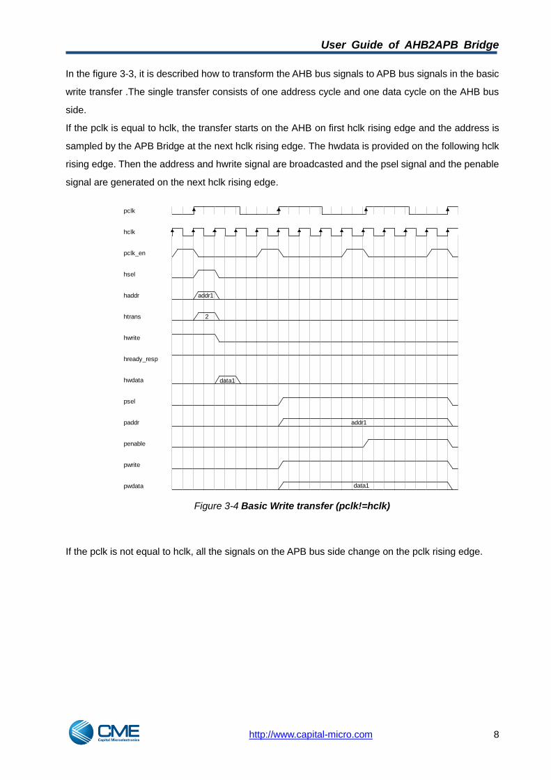
Figure 3-3 Basic Write transfer (pclk=hclk)
User Guide of AHB2APB Bridge
http://www.capital-micro.com 8
In the figure 3-3, it is described how to transform the AHB bus signals to APB bus signals in the basic
write transfer .The single transfer consists of one address cycle and one data cycle on the AHB bus
side.
If the pclk is equal to hclk, the transfer starts on the AHB on first hclk rising edge and the address is
sampled by the APB Bridge at the next hclk rising edge. The hwdata is provided on the following hclk
rising edge. Then the address and hwrite signal are broadcasted and the psel signal and the penable
signal are generated on the next hclk rising edge.
1 2 3 4 5 6 7 8 9 10 11 12 13 14
addr1
addr1
2
data1
data1
TimeGen
pclk
hclk
pclk_en
hsel
haddr
htrans
hwrite
hready_resp
hwdata
psel
paddr
penable
pwrite
pwdata
Figure 3-4 Basic Write transfer (pclk!=hclk)
If the pclk is not equal to hclk, all the signals on the APB bus side change on the pclk rising edge.

User Guide of AHB2APB Bridge
http://www.capital-micro.com 9
1 2 3 4 5 6 7 8 9 10 11
addr1 addr2 addr3 addr4
data1 data2 data3 data4
addr1 addr2 addr3 addr4
data1 data2 data3 data4
2 3 3 3
TimeGen
pclk
hclk
pclk_en
hsel
haddr
htrans
hwrite
hrdata
hready_resp
paddr
pwrite
psel
penable
prdata
Figure 3-5 Read Burst transfer(pclk = hclk)
Figure 3-5 shows how to transform the AHB bus signals to APB bus signals in the read burst transfer.
There are some differences with the single read. All read transfers require a wait state when the
former read operation is not finished and the hready_resp signal will be low in order to make sure that
there is no new address broadcasted. 1 2 3 4 5 6 7 8 9 10 11 12 13 14 15 16 17 18 19 20 21 22 23 24 25 26 27 28 29 30 31
addr1 addr2 addr3
addr1 addr2 addr3
data1 data2 data3
2 3
data1 data2 data3
TimeGen
pclk
hclk
pclk_en
hsel
haddr
htrans
hwrite
hrdata
hready_resp
paddr
pwrite
psel
penable
prdata
Figure 3-6 Read Burst transfer(pclk! = hclk)
User Guide of AHB2APB Bridge
http://www.capital-micro.com 10
If the pclk is not equal to hclk, all the signals on the APB bus side change on the pclk rising edge. 1 2 3 4 5 6 7 8 9 10 11
addr1 addr2 addr3 addr4
data1 data2 data3 data4
addr1 addr2 addr3 addr4
data1 data2 data3 data4
2 3 3 3
TimeGen
pclk
hclk
pclk_en
hsel
haddr
htrans
hwrite
hwdata
hready_resp
paddr
pwrite
psel
penable
pwdata
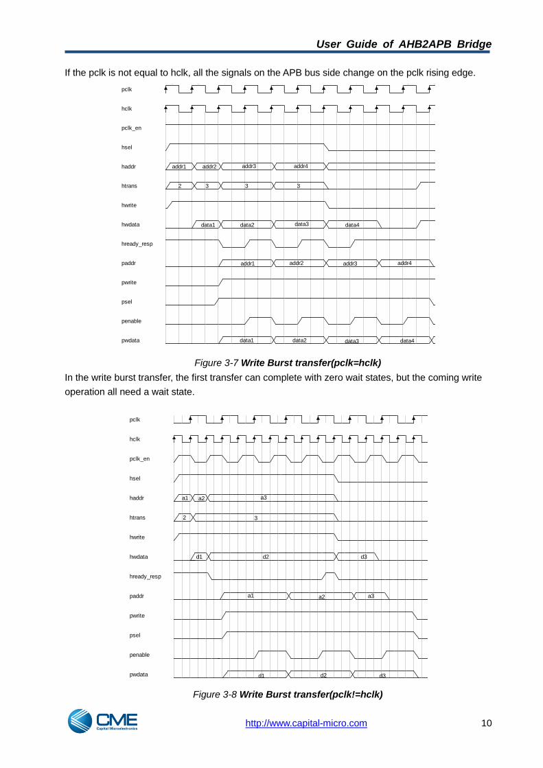
Figure 3-7 Write Burst transfer(pclk=hclk)
In the write burst transfer, the first transfer can complete with zero wait states, but the coming write
operation all need a wait state.
1 2 3 4 5 6 7 8 9 10 11 12 13 14 15 16 17
a1 a2 a3
a1 a2 a3
d1 d2 d3
2 3
d1 d2 d3
TimeGen
pclk
hclk
pclk_en
hsel
haddr
htrans
hwrite
hwdata
hready_resp
paddr
pwrite
psel
penable
pwdata
Figure 3-8 Write Burst transfer(pclk!=hclk)

User Guide of AHB2APB Bridge
http://www.capital-micro.com 11
If the pclk is not equal to hclk, all the signals on the APB bus side change on the pclk rising edge.
3.2 AHB2APB Bridge address mapping
FP0
bfff_ffff
a000_0000
FP1
dfff_ffff
c000_0000
Figure 3-9 Address mapping
The ARM Core provides two groups of AHB Bus signals,AHB0 and AHB1, so there are two memory
space for user logic which are called as FP0 and FP1.It means that if you instantiate an ARM Core
and choose the AHB0 , you must access your slaves on the address from a000_0000 to bfff_ffff, but if
you connect the AHB2APB Bridge to AHB1, the slaves can be accessed on the address from
c000_0000 to dfff_ffff.
The slave number and each slave’s address space can be configured by user. The address space
must be aligned to a 1K boundary, for example, slave0’s address space is from a000_0000 to
a000_03ff.
User Guide of AHB2APB Bridge
http://www.capital-micro.com 12
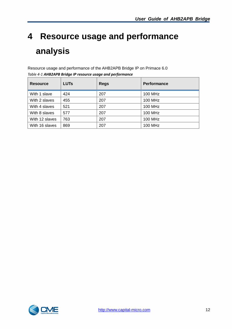
4 Resource usage and performance
analysis
Resource usage and performance of the AHB2APB Bridge IP on Primace 6.0
Table 4-1 AHB2APB Bridge IP resource usage and performance
Resource LUTs Regs Performance
With 1 slave 424 207 100 MHz
With 2 slaves 455 207 100 MHz
With 4 slaves 521 207 100 MHz
With 8 slaves 577 207 100 MHz
With 12 slaves 763 207 100 MHz
With 16 slaves 869 207 100 MHz

User Guide of AHB2APB Bridge
http://www.capital-micro.com 13
5 Generate File Directory Structure
The AHB2APB Bridge IP Wizard generated file includes: source files (src), simulation files(sim) and
example design files and related document. The detailed design directory structure is as below.
Project
src outputs ip_core
ip_top.v
(define by user)
ahb2apb_bridge.v
simsrc doc example
ahb2apb_bridge_tb.v
ahb2apb_bridge_tb_
modelsim.f
ahb2apb_bridge_tb.
do
*.vp
(Protected RTL)
CME_AHB2APB_
Bridge_user_guide
_EN01.pdf
cme_ip_ahb2apb_
bridge_v1_2slaves
CME_AHB2APB_
Bridge_example_user
_guide_EN01.pdf
= directory
= source RTL code
= simulation related files
= documentation
ahb2apb_bridge_v1
src_vp
apb_slave.v
slave_mem_256x32.v
m7a_sim.v
Figure 5-1 IP wizard generated file directory structure
Table 5-1 Generated File Directory structure
Directory Description
src\ Directory for project source code,
including IP wizard generate code.
ip_core\ The directory specially for all IPs
\ahb2apb_bridge_v1 Directory for ahb2apb bridge IP
\doc\CME_AHB2APB_Bridge_user_guide_EN01.doc User guide for ahb2apb bridge IP
\src IP Design RTL

User Guide of AHB2APB Bridge
http://www.capital-micro.com 14
\src\ahb2apb_bridge.v The src of ahb2apb bridge IP
(Encrypted)
\sim
\ahb2apb_bridge_tb.v Testbench of ahb2apb bridge IP
\ahb2apb_bridge_tb_modelsim.f Modelsim simulation related files
\ ahb2apb_bridge_tb.do Do script for Modelsim simulation
\apb_slave.v Other RTL design files for simulation
\ slave_mem_256x32.v
\ m7a_sim.v
\src_vp Protected design RTL for Modelsim
simulation
\*.vp Encrypted ahb2apb bridge IP related
design RTL
\example
ahb2apb_bridge_2slaves.zip Ahb2apb_bridge IP example with 2
salves
CME_AHB2APB_Brdige_example_user_guide
_EN01.pdf
The guide of ahb2apb bridge with 2
slaves.

User Guide of AHB2APB Bridge
http://www.capital-micro.com 15
Revision History
Revision Date Comments
1.0 2013-11-20 Initial release