phased array antenna processing on reconfigurable hardware
TRANSCRIPT
University of TwenteFaculty of Electrical Engineering, Mathematics and
Computer Science
Computer Architecture for Embedded Systems
Phased Array Antenna Processing on
Recon�gurable Hardware
M.Sc. thesis by
Rik Portengen
Graduation committee:prof. dr. ir. Gerard J.M. Smitdr. ir. André B.J. Kokkelerir. Marcel D. van de Burgwalir. Kenneth C. Rovers
Enschede, December 2007

Preface
This thesis presents the results of my work in the research of beam forming
and the creation of a validation platform. During this project the develop-
ment with an evaluation board is experienced. The interface with external
modules delivered some challenges but eventually started to work.
The audio receiving array, the program source codes and this thesis are
part of my master project at the Computer Science department of the Uni-
versity of Twente. The assignment was part of the Beamforce project at the
chair Computer Architecture for Embedded Systems and Thales Hengelo.
I would like to thank my graduation committee for their support. For
getting me this project and to be able to cooperate to get this �nal result.
Marcel van de Burgwal was of great importance to my work for implementing
a Montium version on the evaluation board and to help me with numerous
questions about the interface. Also thanks to the people at Recore Systems
which gave fast updates of the simulator and answers about the Montium
architecture. Further I would like to thank everybody of the CAES group
and students for a really nice time.Finally I would like to thank Linda for her unconditional support during
my master course and this graduation.

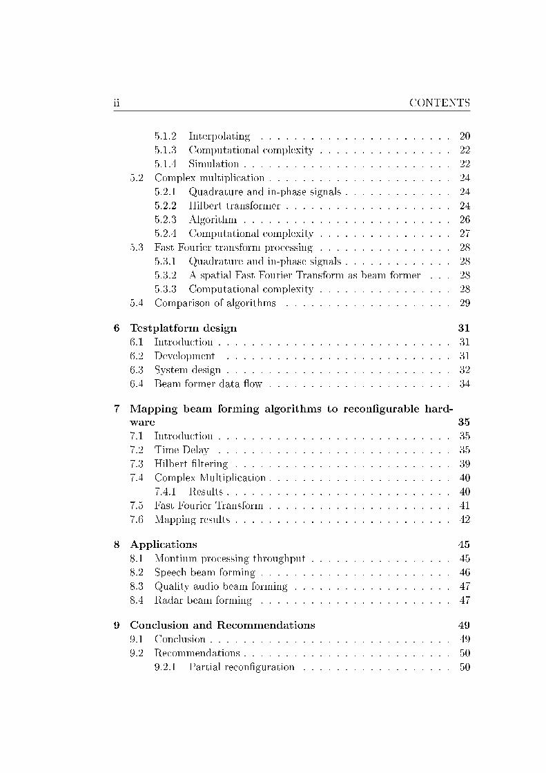
Contents
Introduction v
Introductie vii
1 Phased array antenna processing 1
1.1 Signal Model . . . . . . . . . . . . . . . . . . . . . . . . . . . 11.2 Processing . . . . . . . . . . . . . . . . . . . . . . . . . . . . . 11.3 Problem description . . . . . . . . . . . . . . . . . . . . . . . . 3
2 Literature 5
2.1 Introduction to Radar Systems . . . . . . . . . . . . . . . . . 52.2 Array and Phased Array Antenna Basics . . . . . . . . . . . . 52.3 Smart Antennas . . . . . . . . . . . . . . . . . . . . . . . . . . 6
3 Related work 7
3.1 Radio Astronomy Receivers . . . . . . . . . . . . . . . . . . . 73.2 Optical Beam Forming Networks . . . . . . . . . . . . . . . . 83.3 Mobile Satellite Reception . . . . . . . . . . . . . . . . . . . . 83.4 Base Station Communication . . . . . . . . . . . . . . . . . . 93.5 The Montium, a coarse-grained recon�gurable processor . . . . 9
4 Methods for beam forming 11
4.1 Time delay . . . . . . . . . . . . . . . . . . . . . . . . . . . . 114.2 Phase shift . . . . . . . . . . . . . . . . . . . . . . . . . . . . . 124.3 Butler or FFT transform . . . . . . . . . . . . . . . . . . . . . 144.4 Antenna multiplicity . . . . . . . . . . . . . . . . . . . . . . . 164.5 Beam width and side lobes . . . . . . . . . . . . . . . . . . . . 164.6 Advanced beam steering . . . . . . . . . . . . . . . . . . . . . 16
5 Beam forming algorithms 19
5.1 Time delay . . . . . . . . . . . . . . . . . . . . . . . . . . . . 195.1.1 Algorithm . . . . . . . . . . . . . . . . . . . . . . . . . 19
ii CONTENTS
5.1.2 Interpolating . . . . . . . . . . . . . . . . . . . . . . . 20
5.1.3 Computational complexity . . . . . . . . . . . . . . . . 22
5.1.4 Simulation . . . . . . . . . . . . . . . . . . . . . . . . . 22
5.2 Complex multiplication . . . . . . . . . . . . . . . . . . . . . . 24
5.2.1 Quadrature and in-phase signals . . . . . . . . . . . . . 24
5.2.2 Hilbert transformer . . . . . . . . . . . . . . . . . . . . 24
5.2.3 Algorithm . . . . . . . . . . . . . . . . . . . . . . . . . 26
5.2.4 Computational complexity . . . . . . . . . . . . . . . . 27
5.3 Fast Fourier transform processing . . . . . . . . . . . . . . . . 28
5.3.1 Quadrature and in-phase signals . . . . . . . . . . . . . 28
5.3.2 A spatial Fast Fourier Transform as beam former . . . 28
5.3.3 Computational complexity . . . . . . . . . . . . . . . . 28
5.4 Comparison of algorithms . . . . . . . . . . . . . . . . . . . . 29
6 Testplatform design 31
6.1 Introduction . . . . . . . . . . . . . . . . . . . . . . . . . . . . 31
6.2 Development . . . . . . . . . . . . . . . . . . . . . . . . . . . 31
6.3 System design . . . . . . . . . . . . . . . . . . . . . . . . . . . 32
6.4 Beam former data �ow . . . . . . . . . . . . . . . . . . . . . . 34
7 Mapping beam forming algorithms to recon�gurable hard-
ware 35
7.1 Introduction . . . . . . . . . . . . . . . . . . . . . . . . . . . . 35
7.2 Time Delay . . . . . . . . . . . . . . . . . . . . . . . . . . . . 35
7.3 Hilbert �ltering . . . . . . . . . . . . . . . . . . . . . . . . . . 39
7.4 Complex Multiplication . . . . . . . . . . . . . . . . . . . . . . 40
7.4.1 Results . . . . . . . . . . . . . . . . . . . . . . . . . . . 40
7.5 Fast Fourier Transform . . . . . . . . . . . . . . . . . . . . . . 41
7.6 Mapping results . . . . . . . . . . . . . . . . . . . . . . . . . . 42
8 Applications 45
8.1 Montium processing throughput . . . . . . . . . . . . . . . . . 45
8.2 Speech beam forming . . . . . . . . . . . . . . . . . . . . . . . 46
8.3 Quality audio beam forming . . . . . . . . . . . . . . . . . . . 47
8.4 Radar beam forming . . . . . . . . . . . . . . . . . . . . . . . 47
9 Conclusion and Recommendations 49
9.1 Conclusion . . . . . . . . . . . . . . . . . . . . . . . . . . . . . 49
9.2 Recommendations . . . . . . . . . . . . . . . . . . . . . . . . . 50
9.2.1 Partial recon�guration . . . . . . . . . . . . . . . . . . 50
CONTENTS iii
9.2.2 Scalability . . . . . . . . . . . . . . . . . . . . . . . . . 50
List of Figures 53
A VHDL ADC interface design 55
B Source code of implementation 59
B.1 Time Delay . . . . . . . . . . . . . . . . . . . . . . . . . . . . 59B.2 Phase Shift . . . . . . . . . . . . . . . . . . . . . . . . . . . . 63B.3 Hilbert Filter . . . . . . . . . . . . . . . . . . . . . . . . . . . 68
C Montium tile processor 73
C.1 Introduction . . . . . . . . . . . . . . . . . . . . . . . . . . . . 73C.2 Coarse grain recon�guration . . . . . . . . . . . . . . . . . . . 73C.3 Architecture . . . . . . . . . . . . . . . . . . . . . . . . . . . . 74C.4 Application Development . . . . . . . . . . . . . . . . . . . . . 77

iv CONTENTS
Introduction
In this document the research concerning digital processing of phased arrayantenna signals is described. A study on which algorithms will be suitable forimplementing, how well these perform on a recon�gurable processor and howfast the throughput will be in di�erent scenarios. This thesis will cover themathematical approaches of beam forming and the design decisions taken toperform this task on recon�gurable hardware. In the chapter 1 the generalphased array antenna concept is explained. In chapter 3 reference designsfrom other papers are treated. In chapter 4 the methods for beam formingare described. An algorithm and implementation are made in chapter 5 and7, respectively.
Possible applications and estimated requirements for beam forming sce-narios are given in chapter 8.
A veri�cation platform of beam forming for audio has been designed andimplemented on a development board. This design will be shown in chapter6.
Phased array antenna processing
For reception of electro-magnetic signals an antenna is used. In case of asimple antenna it will receive this signal equally strong from all directions1. Inmany cases this is a usable approach. However, other systems like for examplea satellite communication system or a radio telescope, often a directivitysignal is required. The use of antennas which suppress interference and noiseis then preferred. Traditionally, satellite dishes were used for this but nowalso phased array antennas are slowly introduced as receivers [6, 9].
Phased array antennas consist of multiple antennas spaced from eachother. The use of multiple antennas has a number of advantages. It can beused to improve signal to noise ratio. The phased array antenna has a higher
1A monopole or dipole antenna placed vertical receives all signals equally strong in thehorizontal plane
vi Introduction
sensitivity in the perpendicular direction, this is called a beam. When per-forming processing on the individual antenna signals, it is also possible tosteer the sensitivity of the antenna. This is called beam steering. E�ectively,you can `look' in di�erent directions without mechanically moving the an-tennas. This processing is done digitally in this project. Performing beamforming digitally is commonly referred as Digital Beam Forming (DBF).
Recon�gurable hardware
Hardware can be developed to perform a �xed task. An example is a sound-card in the computer. This hardware is developed to perform the task ofaudio processing; it can perform this task possibly very fast and it could per-form it energy e�ciently. Recon�gurable hardware is developed to performa variety of tasks. The goal of most producers [4] of recon�gurable hardwareis to get an comparable performance with respect to a speci�c applicationdomain as application speci�c hardware. The con�guration of recon�gurablehardware can be altered such that the hardware can execute other tasks. Inthis way, one can use hardware to execute di�erent tasks and take advantageof the recon�gurability.
Introductie
In dit document wordt het onderzoek over digitale verwerkering van fase arrayantenna signalen omschreven. Een studie over welke algorithmes geschiktzijn voor implementatie, hoe goed deze presteren op een recon�gureerbareprocessor en hoe snel de doorvoer capaciteit is in verschillende scenarios. Ditverslag zal de wiskundige aanpak van beam forming uitleggen en de ontwerpbeslissingen die genomen zijn om deze taak op recon�gureerbare hardware uitte voeren. In hoofdstuk 1 is het concept van de fase array antenna uitgelegd.In hoofdstuk 3 zijn referentie ontwerpen van andere verslagen behandeld.In hoofdstuk 4 worden de methodes van beam forming omschreven. Eenalgorithme en implementatie worden gemaakt in de hoofdstukken 5 en 7.
Mogelijke applicaties en verwachte requirements voor verschillende beamforming scenarios worden gegeven in hoofdstuk 8.
Een veri�catie platform voor beam forming met audio is ontworpen engemaakt op een ontwikkel bord. Dit ontwerp wordt in hoofdstuk 6 omschre-ven.
Fase array antenne verwerking
Om radiogolf signalen te ontvangen worden antennes gebruikt. In het gevalvan een simpele antenne zal deze het signaal even sterk ontvangen vanuit allerichtingen2. In veel gevallen is dit een bruikbare aanpak. Echter, andere sys-temen zoals een sateliet communicatie systeem of een radio telescoop hebbenvaak een signaal nodig dat richtings gevoeliger is. Het gebruik van antenneswelke stoorsignalen en ruis onderdrukken is dan gewenst. Traditioneel wer-den hiervoor satellietschotels gebruikt maar tegenwoordig worden ook vakerfase array antennes gebruikt [6, 9].
Fase array antennes bestaan uit meerdere antennes die verdeeld zijn. Hetgebruik van meerdere antennes heeft een aantal voordelen. Ze kunnen ge-
2Een monopool of dipool antenna die verticaal geplaatst is ontvangt alle signalen evensterk in het horizontale vlak
viii Introductie
bruikt worden om ruis te onderdrukken. The fase array antenna heeft eenhogere gevoeligheid in de loodrechte richting, dit is een beam. Wanneerde individuele antennes apart worden verwerkt is het ook mogelijk om degevoeligheid van de antenne te sturen. Dit wordt beam steering (sturing)genoemd. E�ectief, kun je `kijken' in verschillende richtingen zonder hetmechanisch bewegen van de antenne array. De verwerking gaat digitaal indit project. Het digitaal verwerken van beam forming signalen wordt vaakDigital Beam Forming (DBF) genoemd.
Recon�gureerbare hardware
Hardware kan ontworpen worden om een vaste taak uit te voeren. Als voor-beeld hiervan een geluidskaart van een computer; deze hardware is ontwor-pen voor de taak audio verwerking. Het kan deze taak mogelijk heel snel enbijvoorbeeld heel energie e�cient uitvoeren. Recon�gureerbare hardware isontworpen om een verscheidenheid aan taken uit te voeren. Het doel van demeeste producenten [4] van recon�gureerbare hardware is om een vergelijk-bare prestaties te behalen in een speci�ek applicatie domein in vergelijkingmet applicatie speci�eke hardware. De con�guratie van recon�gureerbarehardware is te veranderen en kan dan worden gebruikt voor andere taken.Hierdoor kan hardware meerdere taken uitvoeren en zijn voordeel doen vande recon�gureerbaarheid.
Chapter 1
Phased array antenna processing
A phased array antenna can be designed for a number of applications. Phasedarray antennas are used for example in mobile base stations, radio astronomyreceivers and radar systems. In these applications phased array antennascan apply beam forming to change the sensitivity of the antenna in speci�cdirections and to suppress interference.
1.1 Signal Model
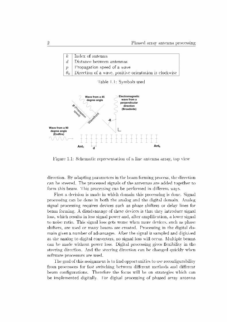
A schematic representation of a phased array antenna system is shown in�gure 1.1. This systems shows a standard setup of a possible array. The arrayis placed in the horizontal plane with antenna elements from west (left) to east(right). A signal coming from the north direction is coming perpendicular tothe array. A signal from the west direction is coming parallel to the array,the array is build of equally spaced antennas. All signals drawn in the �guretravel along the horizontal plane.
The signal arriving at the kth antenna has a delay of
(d/p)sin(−θ0)× k (1.1)
seconds relatively to the �rst antenna. The symbols used in this equationare shown in table 1.1, these symbols will be used throughout this document.The angle θ0 is measured relatively to the perpendicular of the array.
1.2 Processing
The individual antennas of a phased array antenna require processing tocreate a beam in a given direction. A beam represents a signal from a speci�c
2 Phased array antenna processing
k Index of antennad Distance between antennasp Propagation speed of a waveθ0 Direction of a wave, positive orientation is clockwise
Table 1.1: Symbols used
Ant1 Antk
Electromagnetic wave from a
perpendicular direction
(Broadside)
Wave from a 45 degree angle
Wave from a 90 degree angle
(Endfire)
d
-θ
p(Propagation
speed)
Wavefr
ont
Figure 1.1: Schematic representation of a line antenna array, top view
direction. By adapting parameters in the beam forming process, the directioncan be steered. The processed signals of the antennas are added together toform this beam. This processing can be performed in di�erent ways.
First a decision is made in which domain this processing is done. Signalprocessing can be done in both the analog and the digital domain. Analogsignal processing requires devices such as phase shifters or delay lines forbeam forming. A disadvantage of these devices is that they introduce signalloss, which results in less signal power and, after ampli�cation, a lower signalto noise ratio. This signal loss gets worse when more devices, such as phaseshifters, are used or many beams are created. Processing in the digital do-main gives a number of advantages. After the signal is sampled and digitizedat the analog to digital converters, no signal loss will occur. Multiple beamscan be made without power loss. Digital processing gives �exibility in thesteering direction. And the steering direction can be changed quickly whensoftware processors are used.
The goal of this assignment is to �nd opportunities to use recon�gurabilityfrom processors for fast switching between di�erent methods and di�erentbeam con�gurations. Therefore the focus will be on strategies which canbe implemented digitally. For digital processing of phased array antenna
1.3 Problem description 3
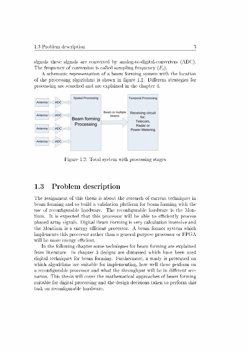
signals these signals are converted by analog-to-digital-converters (ADC).The frequency of conversion is called sampling frequency (Fs).
A schematic representation of a beam forming system with the locationof the processing algorithms is shown in �gure 1.2. Di�erent strategies forprocessing are searched and are explained in the chapter 4.
Spatial ProcessingAntenna ADC
Antenna ADC
Antenna ADC
Antenna ADC
Beam or multiple beams
Temporal Processing
Receiving circuit for;
Telecom,Radar or
Power Metering
Figure 1.2: Total system with processing stages
1.3 Problem description
The assignment of this thesis is about the research of current techniques inbeam forming and to build a validation platform for beam forming with theuse of recon�gurable hardware. The recon�gurable hardware is the Mon-tium. It is expected that this processor will be able to e�ciently processphased array signals. Digital Beam Forming is very calculation intensive andthe Montium is a energy e�cient processor. A beam former system whichimplements this processor rather than a general purpose processor or FPGAwill be more energy e�cient.
In the following chapter some techniques for beam forming are explainedfrom literature. In chapter 3 designs are discussed which have been useddigital techniques for beam forming. Furthermore, a study is presented onwhich algorithms are suitable for implementing, how well these perform ona recon�gurable processor and what the throughput will be in di�erent sce-narios. This thesis will cover the mathematical approaches of beam formingsuitable for digital processing and the design decisions taken to perform thistask on recon�gurable hardware.

4 Phased array antenna processing
Chapter 2
Literature
2.1 Introduction to Radar Systems
The book �Introduction to Radar Systems� [1] explains the basics of radarand radar processing. It covers radar systems and di�erent technologiesto design radar systems. The book also covers noise and clutter (weatherand environmental distortion), which can be observed in practical radars.Chapter 9 explains possible antennas that can be used to create a radarsystem. In this chapter the application of beam forming is explained andhow this can be done in an analog and a digital manner.
In this chapter also a discussion about Baseband and IF Digitizing ismade. When IF Digitizing is used with in-phase and quadrature signals,conversion with two analog to digital converters (ADC) can be done with aminimum sampling rate of 1.4 times the signal (half-power) bandwidth. Itwas stated by [11] that with direct digitizing of the baseband signal with onlyone ADC channel the minimum sampling rate becomes 5.4 times the signalbandwidth. The sampling rate has to be higher than the theoretical Nyquistrate of two times the signal bandwidth for avoiding distortion of the signalspectrum caused by folding.
2.2 Array and Phased Array Antenna Basics
The book �Array and Phased Array Antenna Basics� [2] deals with the basicsof electromagnetic waves and antenna radiation. The �rst three chaptersexplain how single antennas work and introduces their sensitivity. Chapter 4covers the `standard' linear broadside array. This is a standard phased arraybuild up of antennas equally spaced on a straight line. The chapter studies itsperformance and adjustable parameters. It is stated that the �rst side lobe is
6 Literature
around -13 dB of the main beam for a phased array. The remaining chaptersare about di�erent phased array topologies and discusses their designs andperformance. Also how antenna measurements can be performed is written.This book focuses highly on electrical engineering of antennas.
2.3 Smart Antennas
The book �Smart Antennas� [3] introduces array antenna models for di�erentsituations. Narrowband processing, adaptive and broadband processing arethe main chapters. Chapters 2.1 and 2.2 explain conventional beam formingwith a steering vector. This book follows a mathematical approach for theexplanation of beam forming.
Chapter 3
Related work
3.1 Radio Astronomy Receivers
In radio astronomy, the universe is studied about solar systems and stars.One of the methods for observation is to receive electromagnetic waves sendout by stars. The classical approach for this is to use large dish antennas.However, in the search of higher reception quality now also the use of phasedarray antennas is studied.
One example of such an antenna is developed by ASTRON, in [6] a phasedarray antenna telescope demonstrator is described. This demonstrator con-sists of 256 elements and is used for evaluation of the phased array antennaconcept for astronomical research. In this paper a brief description of thethousand element array and the square kilometer array concept is given aswell as results from the demonstrator.
The concept consists of tiles with 64 antennas. These tiles �rst performanalog RF beam forming to create two beams. From there, the result isdown converted, digitized and transported over glas�ber to a digital beamformer. This digital beam former is able to sum di�erent beams and theresult is passed through a Digital Signal Processing (DSP) board. This DSPboard performs the calculations needed for evaluations of the radio astronomysignals.
This design represents certain aspects of the problems encountered inDigital Beam Forming (DBF). The digitalization is done with a sample rateof 40 MHz. ASTRON has chosen to equip the DBF with FPGA's. Currentlythis is a method which is widely used for digital beam forming. [8, 9]
The conclusion is that the demonstrator delivers comparable results withthe current 25m re�ector telescope. Phased array antennas are concluded tobe a well suited technology for radio astronomy telescopes.
8 Related work
3.2 Optical Beam Forming Networks
At the research group �Telecommunication Engineering� of this faculty abeam forming network is developed with the use of laser optics. This iscalled an optical beam forming network (OBFN) [10], the system uses opticalring resonators (ORRs) to establish a continuously tunable time delay. TheOBFN is created by using a binary tree-based hierarchy of ORRs and byusing optical combining/splitting circuitry.
In theory this system can beamform broadband signals because it usestime delay rather than a phase shift. Such an approach can be useful in anumber of applications. An actual design of an OBFN is designed with oneinput and 8 outputs, measurements are performed on a stage of 4 outputs.The design is tuned such that three linearly increasing delays are obtainedover 1.5 GHz bandwidth. The largest delay value is approximately 0.5 ns(corresponding to 15 cm of physical distance in air) and a delay ripple ofapproximately 20 ps (6 mm).
3.3 Mobile Satellite Reception
For the reception of satellite signals often dish antennas are used. Theseantennas need to be setup precisely because of the high angular reception.When pointed directly to a satellite, a signal is received which can be usedfor television or communication. The setup is �xed and can therefore not bemoved, in a mobile situation such high angular reception could be performedwith the use of a phased array antenna.
In �Digital Beam Forming Antenna System for Mobile Communications�[8], which is written in combination with [13], the feasibility of a Digital BeamFormer (DBF) for satellite communication is evaluated. A DSP system isbuilt for the evaluation of reception capabilities of this system. As a referencea Japanese test satellite is used for the reception of an unmodulated signal.The system is built up of 16 antennas and with 128 KHz sampling ADC.Processing is done with FPGA's. These FPGA's are used to implement aDBF using Fast Fourier Transforms. For the creation of quadrature signalsa digital local oscillator is used in combination of a FIR �lter.
The system shows a succesfull implementation of a beam former processorbuilt up of FPGA units. This systems shows a possible implementation of aDBF with the use of a FFT algorithm. This project also shows an adaptivebeam former with a Constant Modulus Algorithm.
3.4 Base Station Communication 9
3.4 Base Station Communication
In the last decade mobile communication has rapidly grown. For mobilecommunication parts of the spectrum are used to transmit and receive signals.Because this is getting used more intensively the spectrum occupation grows,one solution can be to separate transmission signals in space.
A possible implementation of such a solution is written in [7]. It han-dles mobile base communications for ground stations. A cyclic phased arrayantenna is used with patch antennas and an analog beam former network isused for feeding this array. The goal of the project is to increase coverageradius and reduce transmit power of a base station, the cyclic phased arrayantenna has a high gain which is steerable and can be used to accomplishthese goals.
In a satellite communication system separation in space is introduced in[9], supported by ESA/ESTEC in Noordwijk, the Netherlands. The commu-nication system deals with the problems at the satellite site. A phased arrayantenna is mounted on a satellite and uses a system for multiple access fromthe earth. The proposed system features a frequency division multiplexerdemultiplexer with a beam forming network.
This system has high speci�cations, the resources used are limited as onlyone ASIC is used to handle multiple channels. The proposed solution is ahighly integrated system of �lters and Fourier transforms.
3.5 The Montium, a coarse-grained recon�g-
urable processor
The Montium is a processor developed at the University of Twente as partof the Ph.D. thesis of P. Heysters [4]. The Montium can be used as a partof a system on chip. In such a chip, several processors communicate andexchange data with each other. The Montium is therefore also referred to astile processor. Currently the development of this chip and development toolsis handled by Recore Systems [5] which sells this Montium as an IntellectualProperty Core (IP core).
The Montium is developed for streaming applications. These applicationsuse streams of data as input and/or output. The architecture and processingunits are developed to support this kind of applications. The Montium isequipped with 5 ALU's and 10 memories, these memories have a small AGUunit which can generate memory addresses. A complete description of theMontium tile processor can be found in Appendix C.

10 Related work
Chapter 4
Methods for beam forming
The beam forming explained in Chapter 1 is studied in detail and referencedesigns to process signals from phased array antennas. The number of digitalimplementations is limited. In this chapter we restrict to; time delay, phaseshift and Fast Fourier Transform.
4.1 Time delay
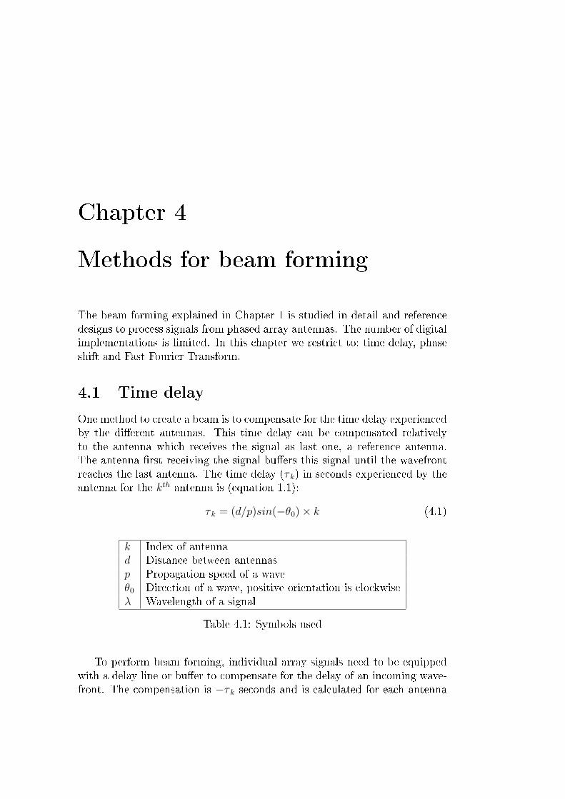
One method to create a beam is to compensate for the time delay experiencedby the di�erent antennas. This time delay can be compensated relativelyto the antenna which receives the signal as last one, a reference antenna.The antenna �rst receiving the signal bu�ers this signal until the wavefrontreaches the last antenna. The time delay (τ k) in seconds experienced by theantenna for the kth antenna is (equation 1.1):
τ k = (d/p)sin(−θ0)× k (4.1)
k Index of antennad Distance between antennasp Propagation speed of a waveθ0 Direction of a wave, positive orientation is clockwiseλ Wavelength of a signal
Table 4.1: Symbols used
To perform beam forming, individual array signals need to be equippedwith a delay line or bu�er to compensate for the delay of an incoming wave-front. The compensation is −τ k seconds and is calculated for each antenna
12 Methods for beam forming
individually. The outputs of the individual delay lines are summed togetherand form one beam. The resolution of this method is dependent on thesmallest time delay, which can be realized by the delay lines.
In the case the signal is compensated relative to an antenna which doesnot receive the signal last, this −τ k will be negative and a negative delayline should be constructed. Such a delay line should contain future signalsand is not feasible. A way to solve this is to add a constant delay equal forall the antennas, which e�ectively compensates relative to the last receivingantenna again.
Time delay works for wideband signals built up of arbitrary frequencies,not only narrowband signals. This is due to the fact that it compensates forthe real experienced di�erences between antennas. This makes the approacha good solution for processing audio signals, because these signals are typi-cally wideband. The response of beam forming methods also depends on thespacing (d) between antennas. In [2] a limit is calculated for the distance d.It is required that d
λ≤ 1 should be satis�ed otherwise grating lobes appear.
In this formula, λ is the wavelength of the signal. Grating lobes are duplicatebeams with the same sensitivity as the main beam, but from unwanted di-rections. The spacing d is taken λ/2, this spacing generates the most numberof nulls without creating ambiguity in the main beam.
As explained in the previous paragraph, beam forming responses are de-pendent on the locations of the antennas with respect to the wavelength ofthe signal. Compensating time delay is said to work for arbitrary frequencies,however, the virtual distance between antennas vary. This is a result fromchanging frequencies and therefore changing wavelengths. The result is thatthe beam width of the main beam depends on the frequency.
4.2 Phase shift
A signal which has only a small bandwidth, can be simpli�ed by a singlesinusoidal signal. This is called the �the narrowband assumption�. For asinusoidal signal, a momentarily value can be recreated by shifting this signalwith the right part of the periodic length. Such part of a period is calledphase. Thus, by changing the phase of a signal it can be shifted in time.
To calculate this phase shift a few values are needed, the distance thatneeds to be compensated and the wavelength of the signal. The wavelengthof the signal is on its turn dependent on the frequency of its signal andthe propagation speed of the wave in its medium. The wavelength (λ) iscalculated by dividing the propagation speed by the frequency of the signal.The frequency will be f and the propagation speed p. In formula form this
4.2 Phase shift 13
will be
λ =p
f(4.2)
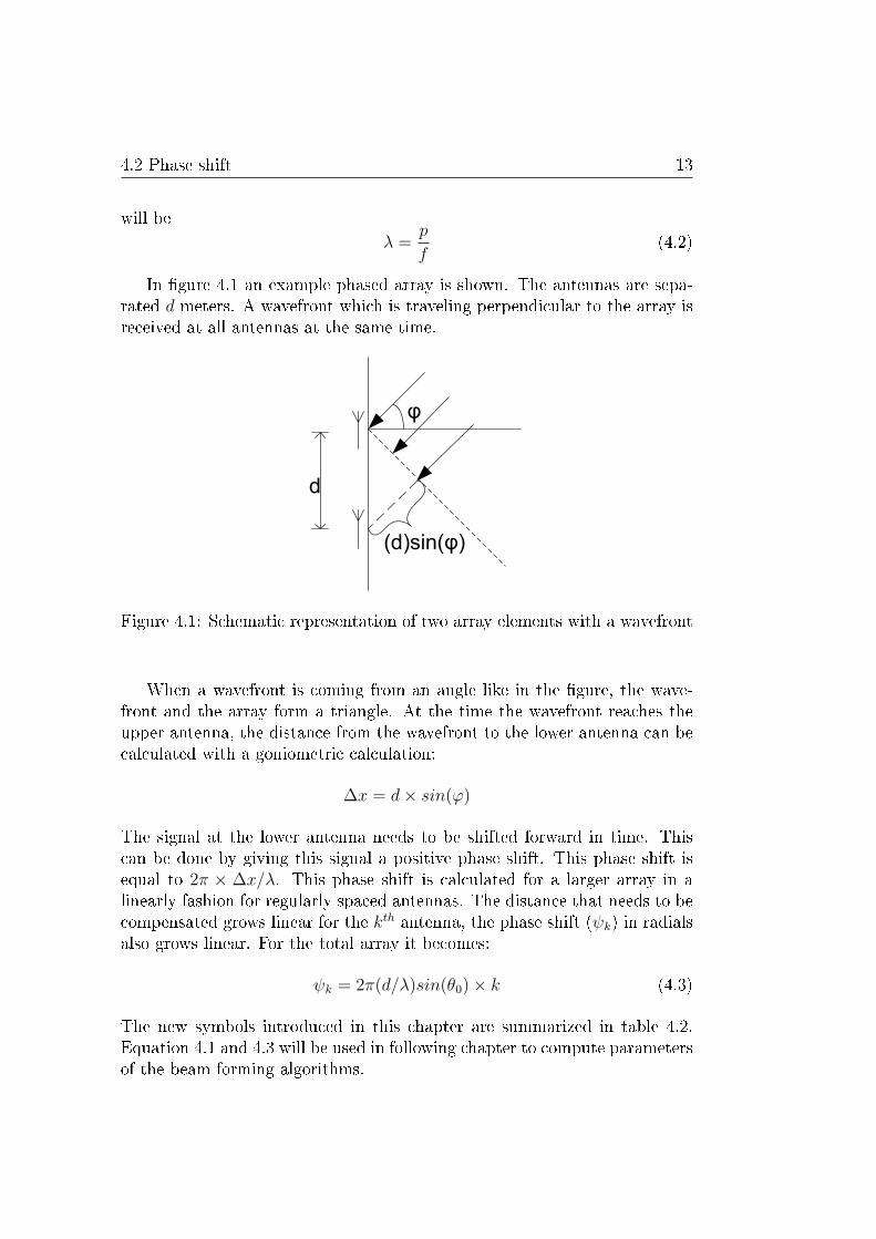
In �gure 4.1 an example phased array is shown. The antennas are sepa-rated d meters. A wavefront which is traveling perpendicular to the array isreceived at all antennas at the same time.
φ
(d)sin(φ)
d
Figure 4.1: Schematic representation of two array elements with a wavefront
When a wavefront is coming from an angle like in the �gure, the wave-front and the array form a triangle. At the time the wavefront reaches theupper antenna, the distance from the wavefront to the lower antenna can becalculated with a goniometric calculation:
∆x = d× sin(ϕ)
The signal at the lower antenna needs to be shifted forward in time. Thiscan be done by giving this signal a positive phase shift. This phase shift isequal to 2π × ∆x/λ. This phase shift is calculated for a larger array in alinearly fashion for regularly spaced antennas. The distance that needs to becompensated grows linear for the kth antenna, the phase shift (ψk) in radialsalso grows linear. For the total array it becomes:
ψk = 2π(d/λ)sin(θ0)× k (4.3)
The new symbols introduced in this chapter are summarized in table 4.2.Equation 4.1 and 4.3 will be used in following chapter to compute parametersof the beam forming algorithms.
14 Methods for beam forming
k Index of antennad Distance between antennasp Propagation speed of a waveθ0 Direction of a wave, positive orientation is clockwiseλ Wavelength of a wave in its mediumτ k Time delayψk Phase shiftFs Sampling frequency
Table 4.2: Updated symbol list
4.3 Butler or FFT transform
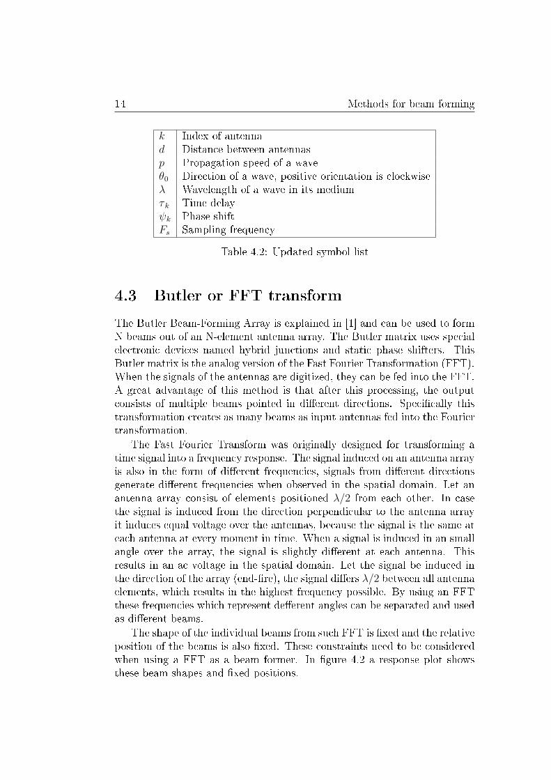
The Butler Beam-Forming Array is explained in [1] and can be used to formN beams out of an N-element antenna array. The Butler matrix uses specialelectronic devices named hybrid junctions and static phase shifters. ThisButler matrix is the analog version of the Fast Fourier Transformation (FFT).When the signals of the antennas are digitized, they can be fed into the FFT.A great advantage of this method is that after this processing, the outputconsists of multiple beams pointed in di�erent directions. Speci�cally thistransformation creates as many beams as input antennas fed into the Fouriertransformation.
The Fast Fourier Transform was originally designed for transforming atime signal into a frequency response. The signal induced on an antenna arrayis also in the form of di�erent frequencies, signals from di�erent directionsgenerate di�erent frequencies when observed in the spatial domain. Let anantenna array consist of elements positioned λ/2 from each other. In casethe signal is induced from the direction perpendicular to the antenna arrayit induces equal voltage over the antennas, because the signal is the same ateach antenna at every moment in time. When a signal is induced in an smallangle over the array, the signal is slightly di�erent at each antenna. Thisresults in an ac voltage in the spatial domain. Let the signal be induced inthe direction of the array (end-�re), the signal di�ers λ/2 between all antennaelements, which results in the highest frequency possible. By using an FFTthese frequencies which represent de�erent angles can be separated and usedas di�erent beams.
The shape of the individual beams from such FFT is �xed and the relativeposition of the beams is also �xed. These constraints need to be consideredwhen using a FFT as a beam former. In �gure 4.2 a response plot showsthese beam shapes and �xed positions.
4.3 Butler or FFT transform 15
−80 −60 −40 −20 0 20 40 60 80−30
−25
−20
−15
−10
−5
0Response of beamforming 16 antennas, d=150m λ=300m
Beamforming angle relative to normal
Am
plitu
de r
espo
nse
(dB
)
Figure 4.2: Response of phased array processing using �t processing, angleof -90 to 90 degrees in 16 steps
−50 0 50−60
−50
−40
−30
−20
−10
0Response of beam forming d=0.5 λ
Angle relative to normal (degrees)
Am
plitu
de r
espo
nse
(dB
)
Figure 4.3: Response of an phase array antenna with 4 (red), 16 (blue) and64 (green) antennas, using complex multiplication to perform beam forming
16 Methods for beam forming
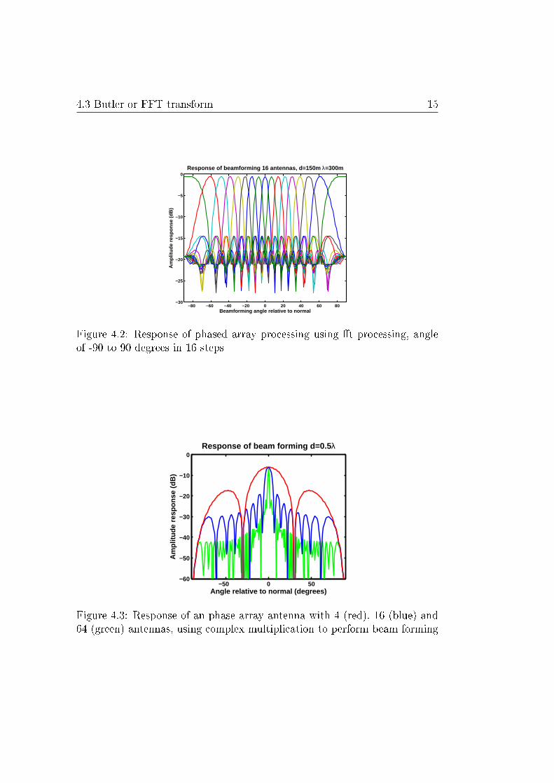
4.4 Antenna multiplicity
The directional sensitivity of the beams created by beam forming are depen-dent of the number of antennas used. By using more antennas the antennasreceive more information about the direction of the signal, which results in ahigher angular resolution. In �gure 4.3 the response of three di�erent phasedarray antenna systems is drawn. One system with four antennas, which hasthe lowest angular resolution. One with 16 antennas, the intermediate andone with 64 antennas, which has the best relative angular resolution. The-3dB bandwidth is 2 degrees.
4.5 Beam width and side lobes
The main beam width and side lobes are dependent on each other. By usingamplitude weighting on the individual antenna elements the shape of themain beam and the side-lobes can be altered. In [2] it is stated that by usinga binomial distribution over the elements, the side lobes can be suppressedall together. However, the resulting main lobe then gets wider. For phaseshifting with complex multiplications this can be applied to all input signals.The shape of the main beam can be tuned. In case multiple beams are createdwith individual sets of coe�cients, all these beams can be tuned individually.What is more interesting is that there is a trade-o� between the width of thebeam and the amount of suppression of the side lobs, depending on the usedweights. The binomial distribution is one extreme of this. This is because ofthe uncertainly principle.
In a FFT approach complex multiplications are re-used. The consequenceis that all beams get the same shape. Individual beam shaping in a FFTapproach is not possible.
The beam width and side lobes also depend on the distribution of theantennas. In this document equal distance between antennas is assumed.Other con�gurations are possible to change the sensitivity of the array andto change beam width, however, this will not be taken into consideration inthis thesis.
4.6 Advanced beam steering
Beam steering can involve a few advanced features, which are treated in [3].For example one of these features involves dynamic nulling. This is a methodto dynamically place the lowest sensitivity in the direction of interference.Adaptive algorithms exist which provide optimal beam steering. A beam

4.6 Advanced beam steering 17
steering algorithm is optimal with respect to an optimization criterium. Anexample criterium could be to produce the highest possible signal to noiseratio. Many of these algorithms work with some sort of digital feedback �lter,in which case the optimal beam steerer dynamically changes the coe�cientsof the beam former.
Such processing can be performed separately of a beam forming algo-rithm. This document will be restricted to beam forming algorithms.

18 Methods for beam forming
Chapter 5
Beam forming algorithms
The previous chapter explained how phased array antenna signals can beprocessed in theory. In this chapter, suitable digital algorithms will be intro-duced to process these signals on a computer: Time Delay, Complex Multi-plication and Fast Fourier Transform.
5.1 Time delay
This method uses processing on the individual signals to create one beam ata time. Through multiple processing stages, multiple beams can be created.The time di�erence introduced by the di�erent locations of the antennas iscompensated with a time shift. After the compensated time shift the signalcan be summed and a beam is created.
5.1.1 Algorithm
The approach is to control the delay signals from individual antenna, whichcan be done with the use of a bu�er. The samples are �rst stored in a bu�erand, when time expires, the samples can be read again. The bu�er is �lledwith a rate equal to the sampling frequency (Fs) and the bu�er is as long asequation 4.1 prescribes. Afterwards the samples are summed.
The bu�er is �lled at a �xed rate every 1/Fs seconds and the delay lengthcan only be made an integer multiple of this time. To be able to construct alldi�erent τ k values as needed, one could try to increase the sampling frequencyFs. However, in case Fs is already high, this solution is not feasible.
20 Beam forming algorithms
5.1.2 Interpolating
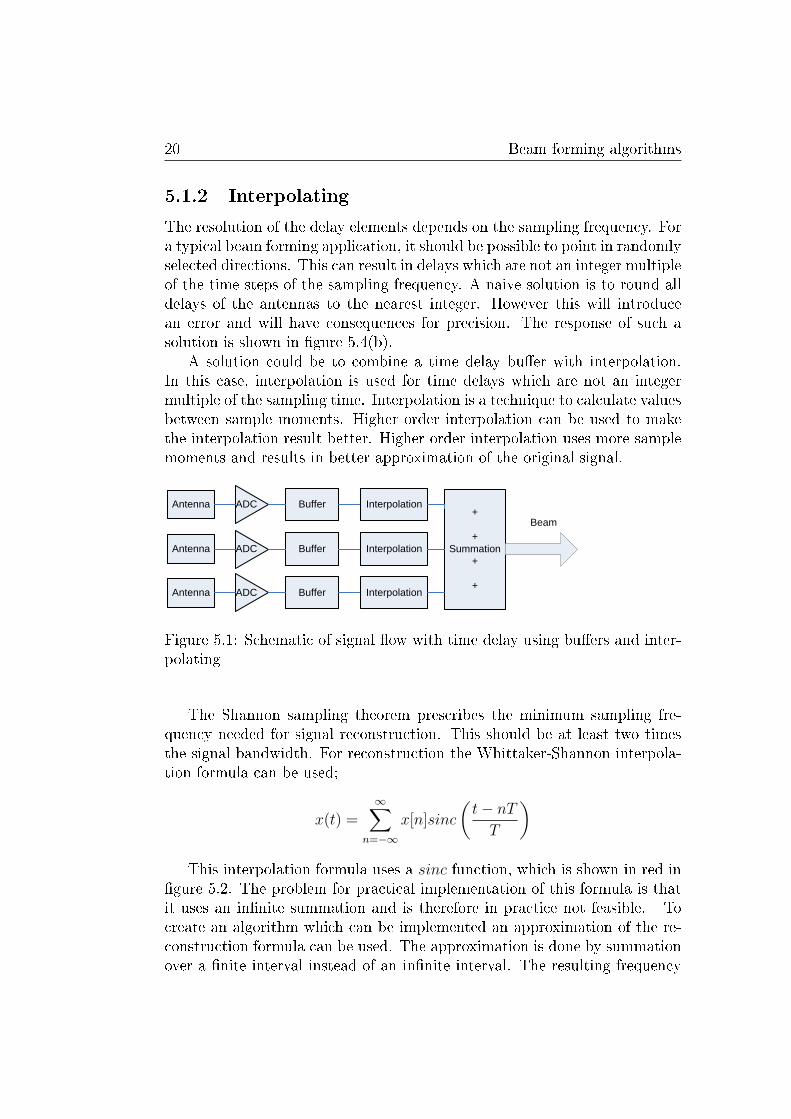
The resolution of the delay elements depends on the sampling frequency. Fora typical beam forming application, it should be possible to point in randomlyselected directions. This can result in delays which are not an integer multipleof the time steps of the sampling frequency. A naive solution is to round alldelays of the antennas to the nearest integer. However this will introducean error and will have consequences for precision. The response of such asolution is shown in �gure 5.4(b).
A solution could be to combine a time delay bu�er with interpolation.In this case, interpolation is used for time delays which are not an integermultiple of the sampling time. Interpolation is a technique to calculate valuesbetween sample moments. Higher order interpolation can be used to makethe interpolation result better. Higher order interpolation uses more samplemoments and results in better approximation of the original signal.
Antenna ADC
Beam
Buffer+
+Summation
+
+
Interpolation
Antenna ADC Buffer Interpolation
Antenna ADC Buffer Interpolation
Figure 5.1: Schematic of signal �ow with time delay using bu�ers and inter-polating
The Shannon sampling theorem prescribes the minimum sampling fre-quency needed for signal reconstruction. This should be at least two timesthe signal bandwidth. For reconstruction the Whittaker-Shannon interpola-tion formula can be used;
x(t) =∞∑
n=−∞
x[n]sinc
(t− nT
T
)This interpolation formula uses a sinc function, which is shown in red in
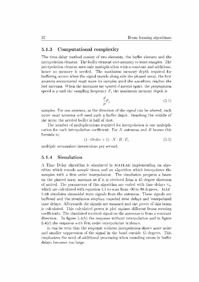
�gure 5.2. The problem for practical implementation of this formula is thatit uses an in�nite summation and is therefore in practice not feasible. Tocreate an algorithm which can be implemented an approximation of the re-construction formula can be used. The approximation is done by summationover a �nite interval instead of an in�nite interval. The resulting frequency
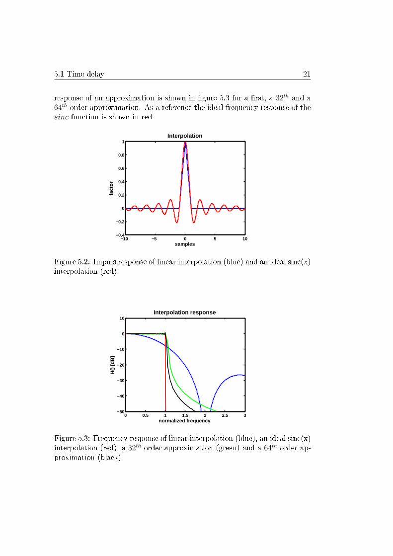
5.1 Time delay 21
response of an approximation is shown in �gure 5.3 for a �rst, a 32th and a64th order approximation. As a reference the ideal frequency response of thesinc function is shown in red.
−10 −5 0 5 10−0.4
−0.2
0
0.2
0.4
0.6
0.8
1Interpolation
samples
fact
or
Figure 5.2: Impuls response of linear interpolation (blue) and an ideal sinc(x)interpolation (red)
0 0.5 1 1.5 2 2.5 3−50
−40
−30
−20
−10
0
10Interpolation response
normalized frequency
H()
[dB
]
Figure 5.3: Frequency response of linear interpolation (blue), an ideal sinc(x)interpolation (red), a 32th order approximation (green) and a 64th order ap-proximation (black)
22 Beam forming algorithms
5.1.3 Computational complexity
The time delay method consist of two elements, the bu�er element and theinterpolation element. The bu�er element uses memory to store samples. Theinterpolation element uses only multiplication with a constant and additions,hence no memory is needed. The maximum memory depth required forbu�ering occurs when the signal travels along side the phased array, the �rstantenna encountered must store its samples until the wavefront reaches thelast antenna. When the antennas are spaced d meters apart, the propagationspeed is p and the sampling frequency Fs the maximum memory depth is
d
pFs (5.1)
samples. For one antenna, as the direction of the signal can be altered, eachouter most antenna will need such a bu�er depth. Reaching the middle ofthe array the needed bu�er is half of that.
The number of multiplications required for interpolation is one multipli-cation for each interpolation coe�cient. For N antennas and B beams thisformula is;
(1 ·Order + 1) ·N ·B · Fs (5.2)
multiply accumulate instructions per second.
5.1.4 Simulation
A Time Delay algorithm is simulated in MATLAB implementing an algo-rithm which rounds sample times and an algorithm which interpolates thesamples with a �rst order interpolation. The simulation projects a beamon the phased array antenna as if it is received from a 45 degree directionof arrival. The parameters of this algorithm are varied with time delays τ k,which are calculated with equation 4.1 to scan from -90 to 90 degrees. MAT-
LAB simulates sinusoidal wave signals from the antennas. These signals arebu�ered and the simulation employs rounded time delays and interpolatedtime delays. Afterwards the signals are summed and the power of this beamis calculated. This calculated power is plot against di�erent beam steeringcoe�cients. The simulated received signal on the antennas is from a constantdirection. In �gure 5.4(b) the response without interpolation and in �gure5.4(c) the response with �rst order interpolation is shown.
It can be seen that the response without interpolation shows more noiseand smaller suppression of the signal in the band outside 45 degrees. Thisemphasizes the need of additional processing when rounding errors in bu�erdelays becomes too large.
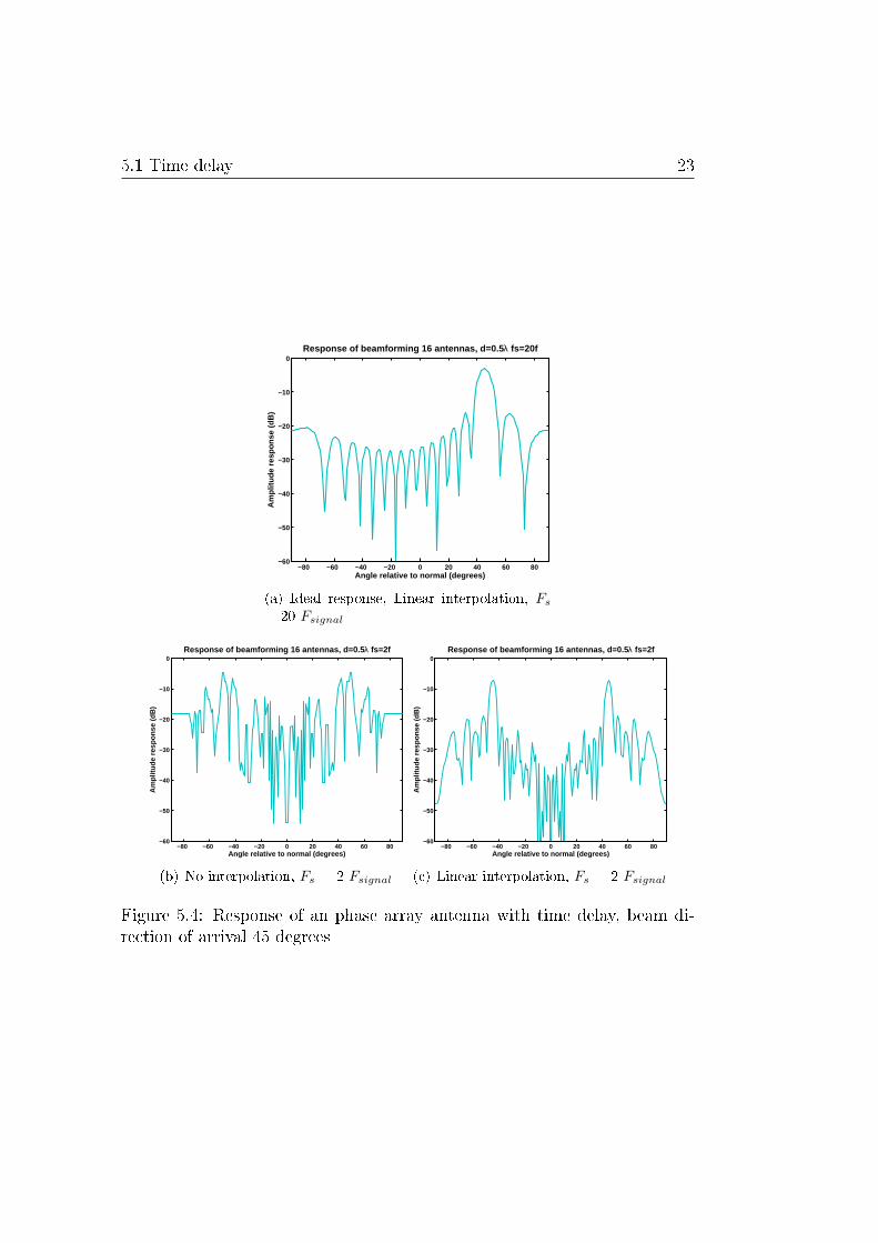
5.1 Time delay 23
−80 −60 −40 −20 0 20 40 60 80−60
−50
−40
−30
−20
−10
0Response of beamforming 16 antennas, d=0.5 λ fs=20f
Angle relative to normal (degrees)
Am
plitu
de r
espo
nse
(dB
)
(a) Ideal response, Linear interpolation, Fs
= 20 Fsignal
−80 −60 −40 −20 0 20 40 60 80−60
−50
−40
−30
−20
−10
0Response of beamforming 16 antennas, d=0.5 λ fs=2f
Angle relative to normal (degrees)
Am
plitu
de r
espo
nse
(dB
)
(b) No interpolation, Fs = 2 Fsignal
−80 −60 −40 −20 0 20 40 60 80−60
−50
−40
−30
−20
−10
0Response of beamforming 16 antennas, d=0.5 λ fs=2f
Angle relative to normal (degrees)
Am
plitu
de r
espo
nse
(dB
)
(c) Linear interpolation, Fs = 2 Fsignal
Figure 5.4: Response of an phase array antenna with time delay, beam di-rection of arrival 45 degrees
24 Beam forming algorithms
5.2 Complex multiplication
The complex multiplication method uses processing on the individual signalsof multiple antennas to create one beam at a time. The phase shift introducedby the spacing of the antennas is compensated with a complex multiplication.After this multiplication all signals from one direction are in phase with eachother and a cumulative signal can be made by adding all signals together.This is under the assumption that narrowband signals are processed.
5.2.1 Quadrature and in-phase signals
For the algorithm to work, every sample in the time domain needs to bemanipulated in phase. The signal gathered by the ADC consists of a realsignal, but does not yet contain phase information in its samples. This canbe seen when a momentarily value is studied. When, for example, a realvalue from the ADC is sampled, its value could be `2'. With this informationit is not possible to know what the phase of a sinusiodional is.
One way to represent complex signals which can include phase informa-tion is using quadrature signals. Together with a real signal, an extra signalis created which lags 90 degrees in phase. For example, when together withthe real `2' an 90 degrees o� `1' signal is present, they represent a phase of
tan
(1
2
)= 27
degrees. So to store phase information in samples a secondary signal isneeded. This signal is called a quadrature signal. In the analog domain, thissignal can be created with the use of a local oscillator (LO); at one side thedirect LO signal and at the other side a 90 degrees shifted LO signal. Thesesignals are multiplied with the received signal and because of this they arecalled in-phase and quadrature signals.
5.2.2 Hilbert transformer
A Hilbert transformer can also be used to construct a quadrature signal withthe in-phase signal as input. This is done by shifting positive frequencies-90 degrees and negative frequencies 90 degrees. In [12] a transformation ismade from the frequency domain to the time domain. The formula whichdescribes the Fourier relation is;
F
(1
πt
)= −j · sgn(f) (5.3)
5.2 Complex multiplication 25
where
sgn(x) =
{1 if x ≥ 0
−1 if x < 0
The right part of equation 5.3 represent the Hilbert function in the fre-quency domain. The positive frequencies get a -90 degrees shift through themultiplication in the frequency domain with −j, while the negative frequen-cies get a multiplication with j in the frequency domain.
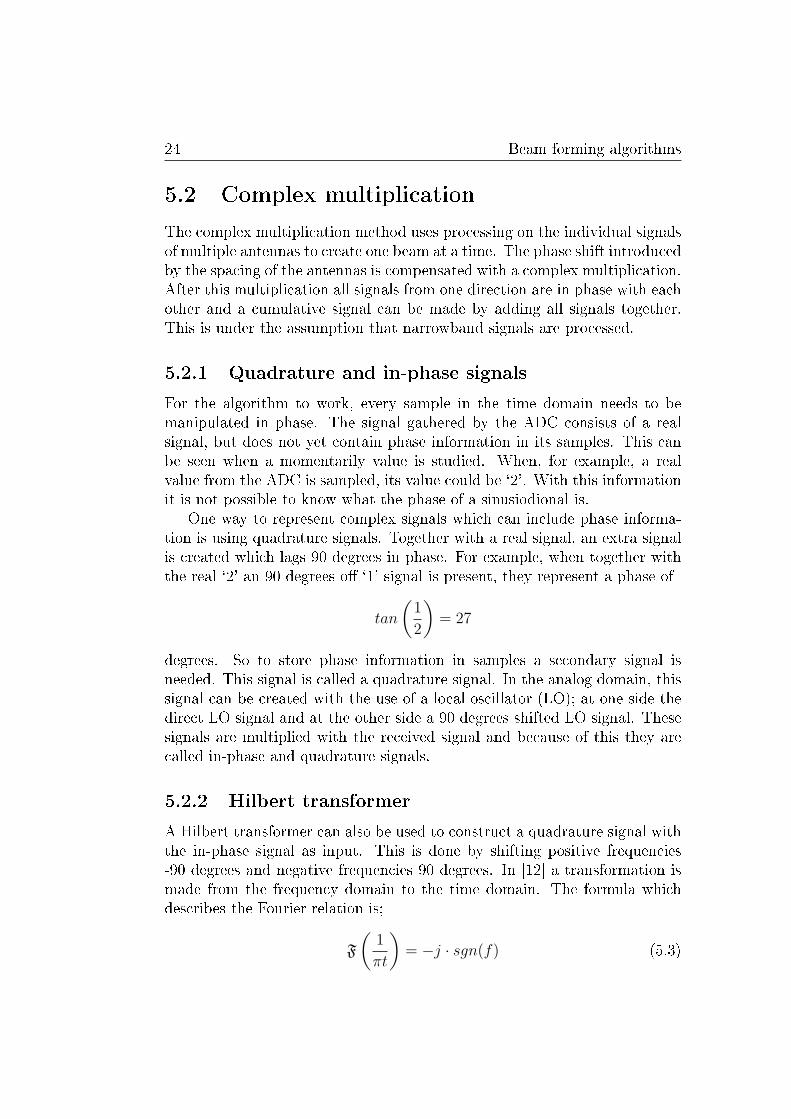
The Fourier transform of the Hilbert function consists of imaginary valuesonly. In the time domain, the function 1/πt can be approximated by a set ofsine waves. By using this time domain function of the Hilbert transformer, itis possible to implement the Hilbert function using a Finite Impuls Response(FIR) �lter. Filter coe�cients can be calculated by MATLAB and an exampleof an impulse response is shown in �gure 5.5.
0 10 20 30 40 50 60−0.8
−0.6
−0.4
−0.2
0
0.2
0.4
0.6
0.8Hilbert impuls response
x
Am
plitu
de
Figure 5.5: Impulse response of a Hilbert �lter
The Hilbert �lter is approximated using a FIR �lter, which introducesextra calculation requirements for the algorithm to �nish. The number ofcalculations required by a FIR �lter depends on the number of coe�cientsused. For every coe�cient a multiply accumulate instruction needs to beexecuted. In general the e�ects of using more coe�cients for FIR �lter designare: the delay of the signal increases, the approximation improves and morecalculations are needed.
26 Beam forming algorithms
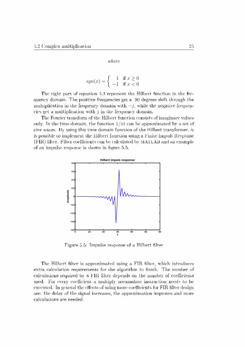
An example Hilbert FIR �lter is designed with MATLAB. It is a 16th order�lter which has 17 coe�cients. The frequency response is shown in �gure 5.6.
0 0.1 0.2 0.3 0.4 0.5 0.6 0.7 0.8 0.9 1−6
−5
−4
−3
−2
−1
0
1
2Hilbert frequency response
Normalized Frequency (x π rad/sample)
Mag
nitu
de (
dB)
Figure 5.6: Frequency response of a Hilbert FIR �lter
As seen in �gure 5.5, half of the coe�cients are zeros. In an optimalimplementation, multiplications where these zero-coe�cients are involved canbe skipped as they do not in�uence the result, resulting in only half themultiply accumulate (MAC) instructions as normal. The example 16th order�lter can with some added control be processed with 8 MAC instructions.
The signal which travels through the Hilbert �lter experiences a groupdelay of half the �lter length. This delay is introduced in FIR �lter design,the FIR �lter applies a convolution with the coe�cients. The coe�cientsrepresent the impulse response of a desired frequency response. Because thisimpulse response is not causal, this impulse response is shifted in time overhalf the �lter length.
The delay must also be given to the in-phase signal. To accomplish this,a group delay block is introduced in the signal path of the in phase signal.
5.2.3 Algorithm
The main algorithm consist of the multiplication of the in phase and quadra-ture signal (from now on the combination of these signals is called a complexsignal) with a phase shifting vector (ρk). This vector is given a magnitude of
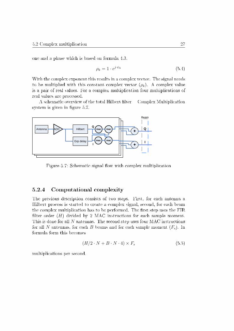
5.2 Complex multiplication 27
one and a phase which is based on formula 4.3.
ρk = 1 · ej·ψk (5.4)
With the complex exponent this results in a complex vector. The signal needsto be multiplied with this constant complex vector (ρk). A complex valueis a pair of real values. For a complex multiplication four multiplications ofreal values are processed.
A schematic overview of the total Hilbert �lter + Complex Multiplicationsystem is given in �gure 5.7.
Beam
Q
I
Antenna ADC
Grp delay
HilbertQ
I
mac mac
mac mac
Figure 5.7: Schematic signal �ow with complex multiplication
5.2.4 Computational complexity
The previous description consists of two steps. First, for each antenna aHilbert process is started to create a complex signal, second, for each beamthe complex multiplication has to be performed. The �rst step uses the FIR�lter order (H) divided by 2 MAC instructions for each sample moment.This is done for all N antennas. The second step uses four MAC instructionsfor all N antennas, for each B beams and for each sample moment (Fs). Informula form this becomes
(H/2 ·N +B ·N · 4)× Fs (5.5)
multiplications per second.
28 Beam forming algorithms
5.3 Fast Fourier transform processing
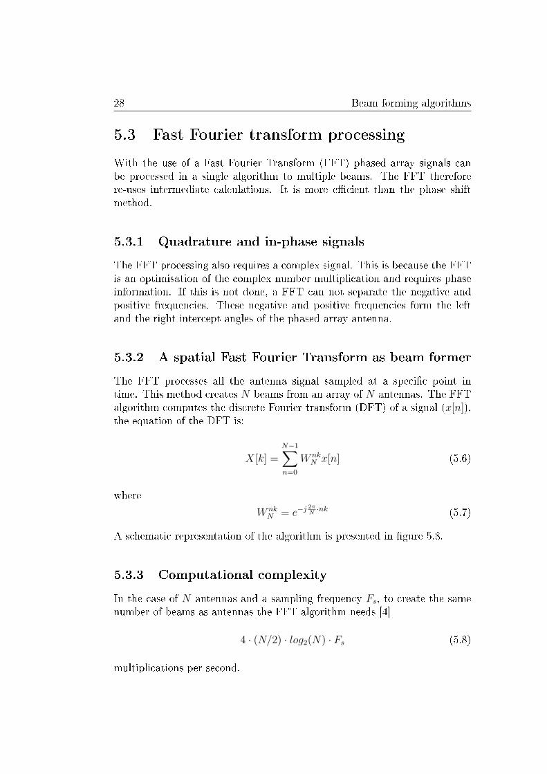
With the use of a Fast Fourier Transform (FFT) phased array signals canbe processed in a single algorithm to multiple beams. The FFT thereforere-uses intermediate calculations. It is more e�cient than the phase shiftmethod.
5.3.1 Quadrature and in-phase signals
The FFT processing also requires a complex signal. This is because the FFTis an optimisation of the complex number multiplication and requires phaseinformation. If this is not done, a FFT can not separate the negative andpositive frequencies. These negative and positive frequencies form the leftand the right intercept angles of the phased array antenna.
5.3.2 A spatial Fast Fourier Transform as beam former
The FFT processes all the antenna signal sampled at a speci�c point intime. This method creates N beams from an array of N antennas. The FFTalgorithm computes the discrete Fourier transform (DFT) of a signal (x[n]),the equation of the DFT is:
X[k] =N−1∑n=0
W nkN x[n] (5.6)
where
W nkN = e−j
2πN·nk (5.7)
A schematic representation of the algorithm is presented in �gure 5.8.
5.3.3 Computational complexity
In the case of N antennas and a sampling frequency Fs, to create the samenumber of beams as antennas the FFT algorithm needs [4]
4 · (N/2) · log2(N) · Fs (5.8)
multiplications per second.
5.4 Comparison of algorithms 29
Antenna ADCI and Q pair
Beams
Grp delay
HilbertQ
I
Antenna ADC
Grp delay
HilbertQ
I
SpatialFast Fourier Transform
I and Q pair
Figure 5.8: Schematic signal �ow with FFT processing
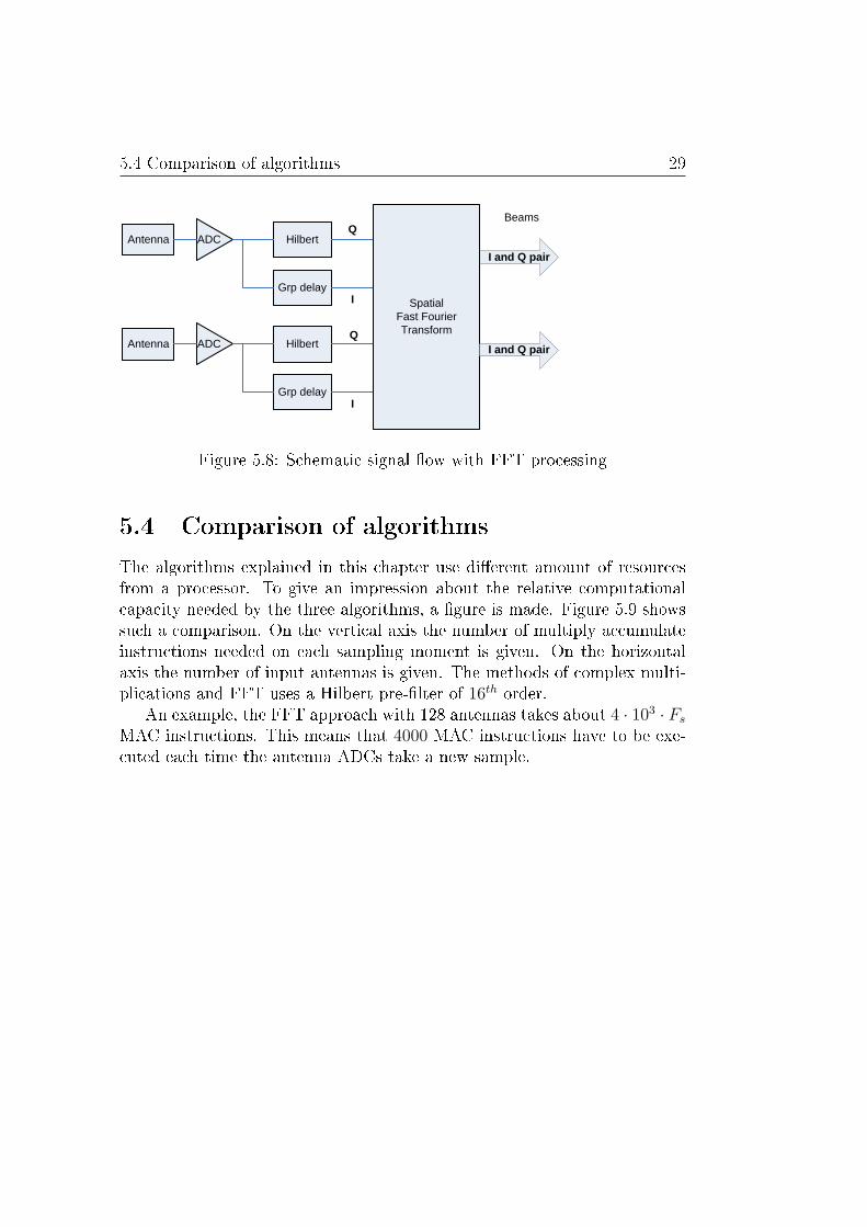
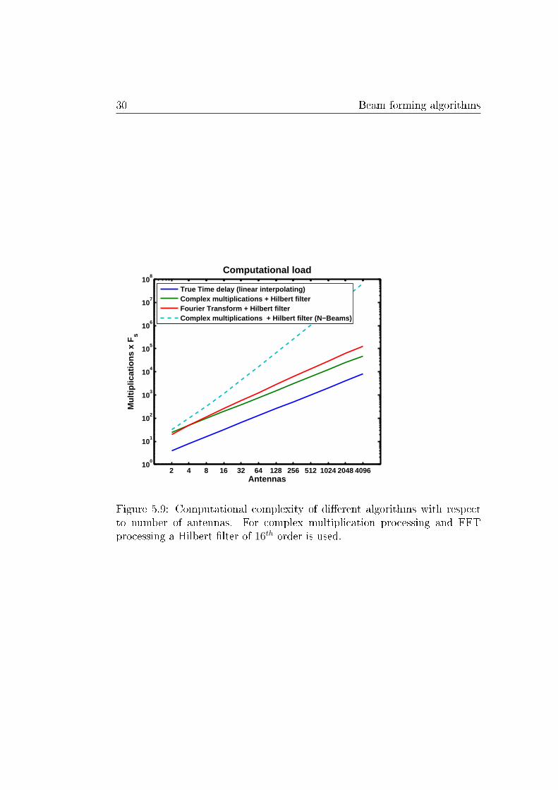
5.4 Comparison of algorithms
The algorithms explained in this chapter use di�erent amount of resourcesfrom a processor. To give an impression about the relative computationalcapacity needed by the three algorithms, a �gure is made. Figure 5.9 showssuch a comparison. On the vertical axis the number of multiply accumulateinstructions needed on each sampling moment is given. On the horizontalaxis the number of input antennas is given. The methods of complex multi-plications and FFT uses a Hilbert pre-�lter of 16th order.
An example, the FFT approach with 128 antennas takes about 4 · 103 · FsMAC instructions. This means that 4000 MAC instructions have to be exe-cuted each time the antenna ADCs take a new sample.
30 Beam forming algorithms
2 4 8 16 32 64 128 256 512 1024 2048 409610
0
101
102
103
104
105
106
107
108
Antennas
Mul
tiplic
atio
ns x
Fs
Computational load
True Time delay (linear interpolating)Complex multiplications + Hilbert filterFourier Transform + Hilbert filterComplex multiplications + Hilbert filter (N−Beams)
Figure 5.9: Computational complexity of di�erent algorithms with respectto number of antennas. For complex multiplication processing and FFTprocessing a Hilbert �lter of 16th order is used.
Chapter 6
Testplatform design
6.1 Introduction
The test platform is built on a development board of Xilinx [17]. This de-velopment board has a FPGA, a number of input, output peripherals andis equipped with hardware to build an embedded system. The FPGA is aVirtex II Pro, this FPGA has next to the standard FPGA slices also blockRAMs, multiplier slices and two PowerPCs. A PowerPC is a general pur-pose processor. For a beam forming testplatform audio signals are takento be evaluated. Audio signal can be made with a predetermined spectrumand with the use of microphones these signals can be received. The receivedanalog signal is converted with analog to digital converts (ADC) to a digitalsignal. These digital signals lines are connected to the FPGA.
6.2 Development
Developing a system on the development board can be done with the use ofthe Xilinx Platform Studio (XPS) software [18]. The studio delivers supportfor a hardware project with multiple software projects. The project is usuallystarted with a �base system builder� wizards [16] which gives a foundationfor the rest of the project. The wizard needs a �User Peripheral Repository�which gives a description of the development board. The output of thewizard consists of a complete (compilable) project which can be downloadedfor evaluation.
This package of software delivers multiple tools for designing and debug-ging a hardware software integrated system. The XPS software is used tocreate a design for beam forming with the Montium and the ADCs. The twomost used software programs in this package are;
32 Testplatform design
Impact
Impact is a tool that can be used to program the development platform.This tool support all methods for con�guring and handles the �le translationbetween di�erent formats. The board can be con�gured in a number of ways,for example, it can directly be programmed through the embedded platformUSB connection, it can be con�gured with the use of the onboard �ash PROMor it can be con�gured with the use of a Compact Flash card. Downloadingsoftware is done using Boundary Scan (IEEE 1149.1 /IEEE 1532).
Integrated Software Environment
The �Integrated Software Environment� (ISE) is the environment used byXPS to synthesize hardware designs. The hardware designs (for exampleVHDL descriptions) are managed by XPS and are compiled with this pro-gram. The input is a hardware description language and the output are netlists and place-and-route information.
6.3 System design
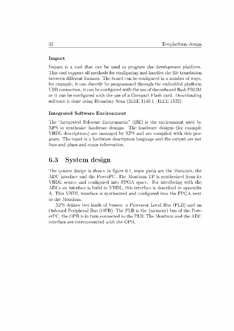
The system design is shown in �gure 6.1, main parts are the Montium, theADC interface and the PowerPC. The Montium TP is synthesized from itsVHDL source and con�gured into FPGA space. For interfacing with theADCs an interface is build in VHDL, this interface is described in appendixA. This VHDL interface is synthesized and con�gured into the FPGA nextto the Montium.
XPS de�nes two kinds of busses: a Processor Local Bus (PLB) and anOnboard Peripheral Bus (OPB). The PLB is the (memory) bus of the Pow-erPC, the OPB is in turn connected to the PLB. The Montium and the ADCinterface are interconnected with the OPB.
6.3 System design 33
Pro
cess
or L
ocal
Bus
(PLB
)O
nboa
rd P
erip
hera
l Bus
(OP
B)
PLB 2 OPB
Montium Tile Processor
0x80.00.00.00 (256M)
OPB ADC Interface
0x40.70.00.00 (64K)0x40.60.00.00 (64K)RS-232 Interface
0x40.00.00.00 (1G)
PowerPC
PLB: 32 bits addressing
Instruction mem
Data memory
0xff.fe.00.00 (128K)
0x21.80.00.00 (64K)
AD module
micmic
AD module
micmic
AD module
micmic
AD module
micmic
Figure 6.1: Hardware design of the testplatform
34 Testplatform design
6.4 Beam former data �ow
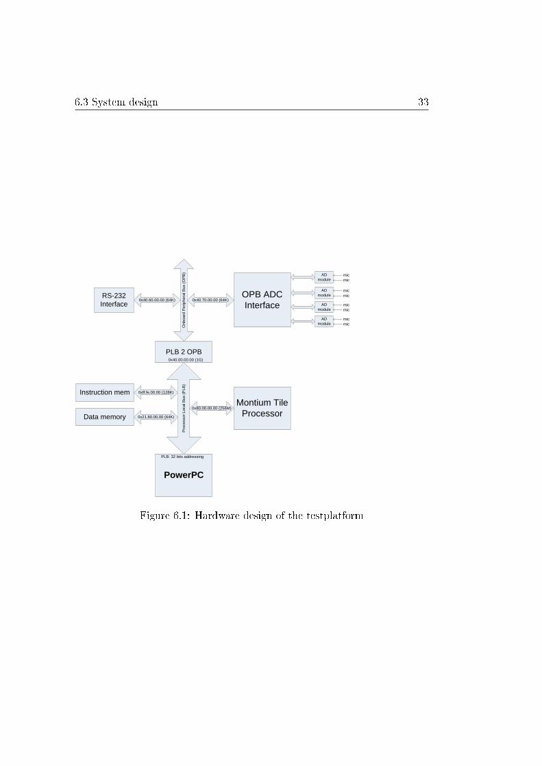
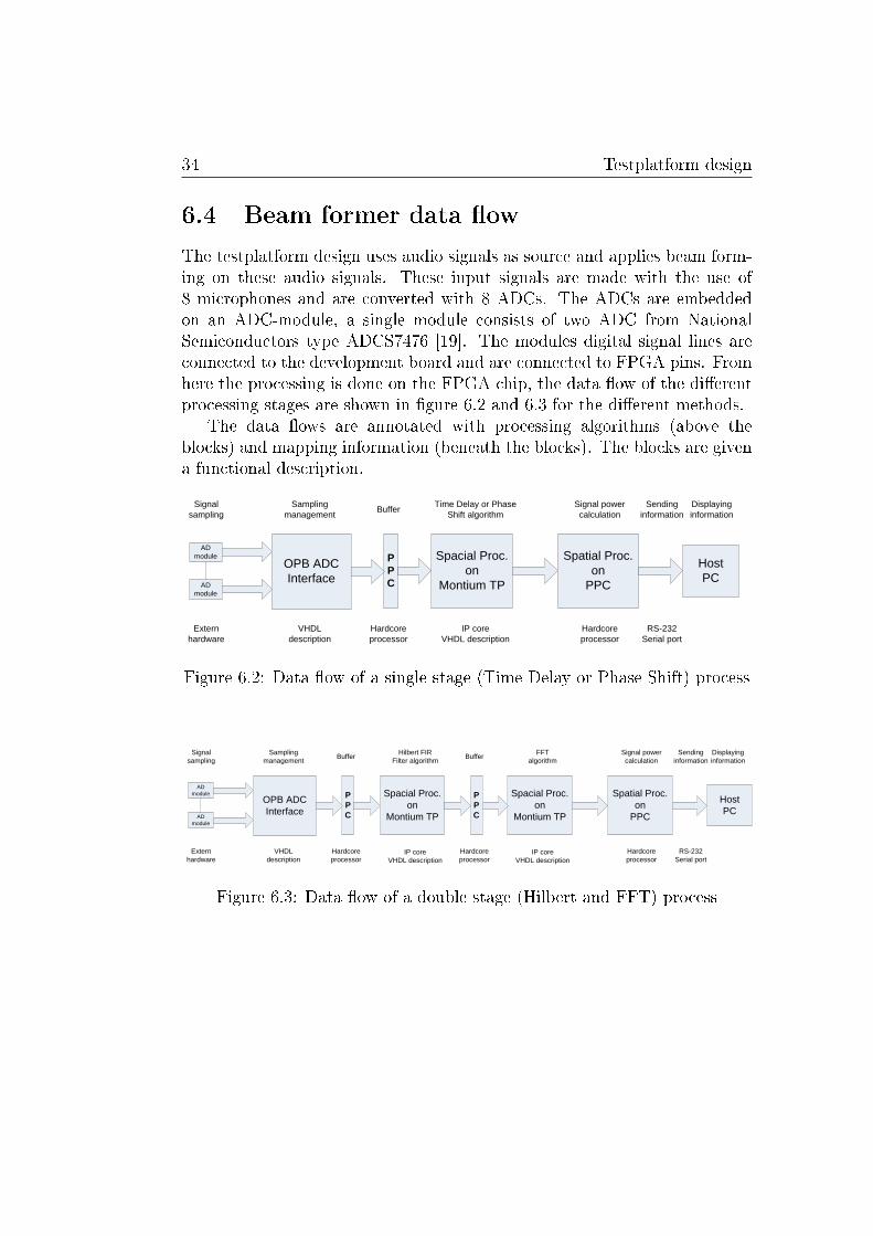
The testplatform design uses audio signals as source and applies beam form-ing on these audio signals. These input signals are made with the use of8 microphones and are converted with 8 ADCs. The ADCs are embeddedon an ADC-module, a single module consists of two ADC from NationalSemiconductors type ADCS7476 [19]. The modules digital signal lines areconnected to the development board and are connected to FPGA pins. Fromhere the processing is done on the FPGA chip, the data �ow of the di�erentprocessing stages are shown in �gure 6.2 and 6.3 for the di�erent methods.
The data �ows are annotated with processing algorithms (above theblocks) and mapping information (beneath the blocks). The blocks are givena functional description.
AD module
AD module
OPB ADC Interface
PPC
Spacial Proc. on
Montium TP
Spatial Proc. on
PPC
Extern hardware
VHDL description
Hardcoreprocessor
IP coreVHDL description
Hardcoreprocessor
HostPC
RS-232Serial port
Signalsampling
Samplingmanagement Buffer Time Delay or Phase
Shift algorithmSignal powercalculation
Sending information
Displaying information
Figure 6.2: Data �ow of a single stage (Time Delay or Phase Shift) process
AD module
AD module
OPB ADC Interface
PPC
Spacial Proc. on
Montium TP
Spatial Proc. on
PPC
Extern hardware
VHDL description
Hardcoreprocessor
IP coreVHDL description
Hardcoreprocessor
HostPC
RS-232Serial port
Signalsampling
Samplingmanagement Buffer FFT
algorithmSignal powercalculation
Sending information
Displaying information
Spacial Proc. on
Montium TP
IP coreVHDL description
Hilbert FIRFilter algorithm
PPC
Hardcoreprocessor
Buffer
Figure 6.3: Data �ow of a double stage (Hilbert and FFT) process
Chapter 7
Mapping beam forming
algorithms to recon�gurable
hardware
7.1 Introduction
This chapter will show how the previously explained algorithms have beenimplemented on the Montium processor. First the Time Delay algorithmimplementation is explained. Then the implementation of a Hilbert �ltertogether with the Complex Multiplication. Finally it is shown how the resultsof the Hilbert �lter can be used for the Fast Fourier Transform.
The algorithm implementations are made for a system with 8 input an-tennas/channels.
7.2 Time Delay
The Time Delay algorithm consists of bu�ering, interpolation and summa-tion. The following implementation is for a system which consists of 8 an-tennas, also called channels in this text. A trade o� is made which combinesinterpolation with a feasible amount of processor power. The implementationmade is an algorithm which uses a linear interpolation. Linear interpolationstores two samples in the registers and gives weights corresponding linearlyto the distance of the required time and the sampling time. The resultingfrequency response of this implementation is shown in �gure 5.3.
The Montium receives samples, one sample Xk,i for each channel (k) foreach sampling time (i) and outputs a single value for each sampling time.The output sample Yi is the calculated beam.
36 Mapping beam forming algorithms to recon�gurable hardware
In the following sections these steps are explained. The steps are fora single channel. The Montium is a parallel machine and the steps canbe performed for 5 channels in parallel; each Processing Part handles onechannel at a time.
Bu�ering
Bu�ering is done with the use of a cyclic bu�er. This bu�er uses the memoriesof the Montium. Each channel is given its own memory, because the Montiumis equipped with 10 memories it can serve 10 channels. A cyclic bu�er isformed by incrementing the pointers with a modulo function. Two pointersare introduced, one writepointer which stores the location where the bu�eris �lled and one readpointer where the bu�er is read.
The pointers are stored in registers of the ALU. When a sample is calcu-lated these pointer are incremented. In each iteration, incoming samples (X)are stored at the position of the writepointer and a sample at the readpointeris forwarded to a register (R).
Interpolation
The sample stored in the register is multiplied with an interpolation coe�-cient and stored in a register, mathematical:
A = R[n] · Cinterpolation[1]
In the CDL1 code the interpolation coe�cients Cinterpolation[1] and Cinterpolation[2]are called FIRST and SECOND, respectively. In CDL code the interpolation is:
// Multiply NEWREGm1 (c1) sample with FIRSTm1 coeff. (b2)
alu p3c1 fmul p3b2 sadd p3es -> p3ws
In the next clock cycle the previous sample X[n − 1] = R[n − 1] is usedand multiplied with the second interpolation coe�cient. In the same clockcycle this value is added to the previously calculated value A:
I = R[n− 1] · Cinterpolation[2] + A
clock
// Multiply OLDREGm1 (b1) sample with SECONDm1 coeff. (c2)
alu p3b1 fmul p3c2 sadd p3es -> p3ws
Now an interpolated sample I is calculated for this channel. This sample(Ik,i) is used for summation.
1Montium source code
7.2 Time Delay 37
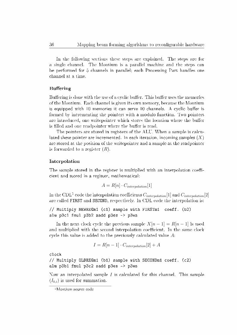
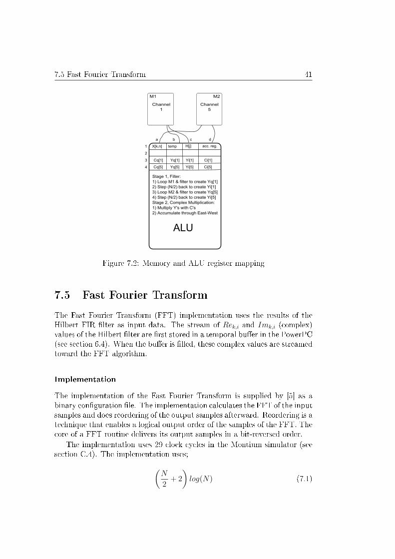
Figure 7.1: Memory and ALU register mapping
Summation
Summation is done by adding all samples Ik,i from the di�erent processingparts together to form the resulting output sample Yi. Summation is donewith the use of the east-west connections of the ALUs. The summation of dif-ferent processing parts is done in parallel with interpolation. The calculatedvalue A becomes then a cumulative value for 4 channels and is calculated byadding Ik,i for k = 0 to 3. In the second stage (channels 4 to 7) this value isadded with Ik,i for k = 4 to 7.
In the �rst stage;
Yi =3∑
k=0
Yk,i
and in the second stage;
Yi =7∑
k=4
Yk,i + Yi
The output sample Yi is a sample for the beam calculated.

38 Mapping beam forming algorithms to recon�gurable hardware
Clock cycles
The algorithm on the Montium uses 10 cycles for one output sample2. Thiscan only be seen in the source code, provided in appendix B. For the mul-tiplication 4 cycles are used, 4 more for pointer updating and 2 for input,output communications.
2The Montium processor is a complex processor which can do a lot in parallel. Theexplanation of the mapping is not a one to one mapping in clock cycles. Because ofperformance enhancement, re-ordering and re-scheduling of processing is performed.
7.3 Hilbert �ltering 39
7.3 Hilbert �ltering
The complex multiplication implementation is made with a preprocessorwhich �lters the incoming data. This �lter is a Hilbert FIR �lter whichgenerates information about the phase of the signal received. This Hilbert�lter is implemented as a FIR �lter in an optimized way. And is capable toprocess multiple channels in parallel.
The Montium receives as before a sample (Xk,i) for each channel (k)every sampling time (i). These samples are �ltered and the Hilbert stagewill output two values: the �ltered quadrature (Im) value and the in-phasevalue (Re).
The number of samples which have to be calculated is preferred to be apower of 2. This results in an e�cient mapping on the Montium AGUs. Theimplemented Hilbert �lter is a 16th order �lter. The �lter coe�cients (Cj) arecalculated by MATLAB. This results in 17 coe�cients of which 9 (rounded tothe nearest 16 bits number representation) are zero, 8 coe�cients remain tobe calculated by the processor. The frequency response of a 16th order �lteris given in �gure 5.6.
Bu�ering
First the Hilbert �lter bu�ers the incoming samples Xi in a cyclic bu�er(which is a modi�ed version of [14]). The algorithm is made for 8 inputchannels in the spatial domain which are stored in the �rst 8 memories ofthe Montium. These bu�ers are split in two sections of which the odd andeven temporal index (i) of Xk,i are separated. In the current implementation,these odd and even samples are split up in two partitions of the memory, each8 samples long.
Filtering
The Hilbert coe�cients (Cj) are stored in an additional memory, memory 9,of the processor. This memory is used by all processing parts to multiply theincoming data with.
Imk,i = Xk,(i−j) · Cj + Imk,i for j = 1 till 8
Group delay
This implementation also generates a value for the in-phase signal. Thisvalue is calculated by addressing the cyclic bu�er half the order of samples
40 Mapping beam forming algorithms to recon�gurable hardware
back.Rek,i = Xk,(i−O/2) for O = Order of �lter
Clock cycles
The algorithm on the Montium uses 21 cycles for one sampling time. Forthe multiplication 2 · 8 cycles are used, 2 for overhead of pointers and 3 forinput, output communications.
7.4 Complex Multiplication
The output of the Hilbert �lter is stored in registers. The complex multi-plication (CM) continues processing with these values. It should multiplythe complex signal pairs (Im and Re) with complex coe�cients. It does thisonly to the extend that it calculates the resulting real values (Re). The re-sult of the imaginary value (Im) is not calculated. This is done because thepost-processing stage, power calculation, does not require a complex signal.
Clock cycles
The algorithm on the Montium uses 7 cycles for one sampling time. For themultiplication of 8 complex signal pairs with 8 coe�cients 5 cycles are used,1 for overhead and 1 for input, output communications.
A complex signal pair multiplication requires 4 clock cycles on one pro-cessing part, now only 2 clock cycles are used. Because one processing parthandles two channels, the processing parts need 4 clock cycles. For the �nalsummation of all 8 signals the accumulated results of the processing partsare added in a �nal summation clock cycle.
7.4.1 Results
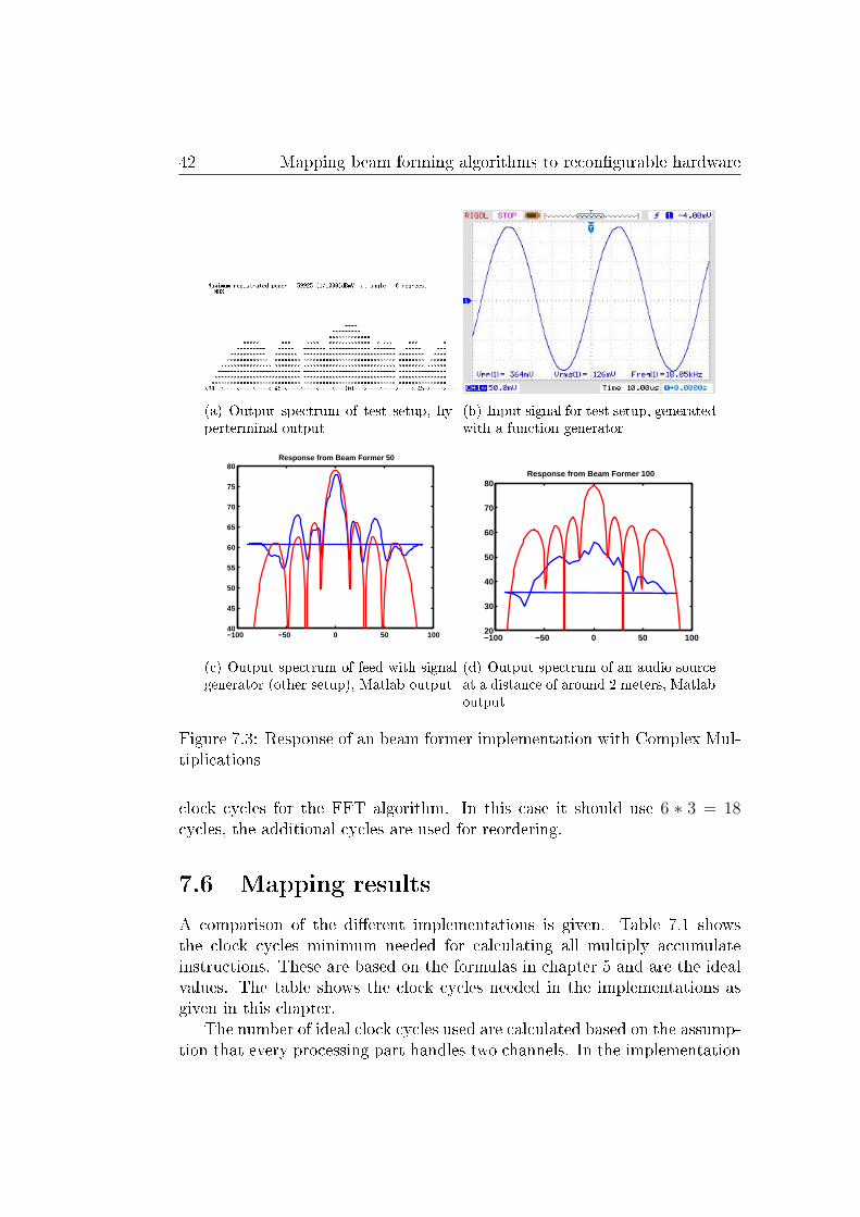
The test setup is made with the development board (chapter 6) and theMontium con�guration for CM.
The test is made with a signal generator, generating a sinus with a RMSvalue of 126mV (�gure 7.3(b)). This signal is split in 8 and fed throughthe inputs of the ADC and is beam formed in the Montium processor. ThePowerPC calculates the power received. This test signal should result in apower of
20 ∗ log(126mV × 8) = 60.069dBmV
In �gure 7.3(a) the output signal in shown and a value of 59.925 in calculatedby the PowerPC. This result shows a large resemblance with what is expected.
7.5 Fast Fourier Transform 41
Figure 7.2: Memory and ALU register mapping
7.5 Fast Fourier Transform
The Fast Fourier Transform (FFT) implementation uses the results of theHilbert FIR �lter as input data. The stream of Rek,i and Imk,i (complex)values of the Hilbert �lter are �rst stored in a temporal bu�er in the PowerPC(see section 6.4). When the bu�er is �lled, these complex values are streamedtoward the FFT algorithm.
Implementation
The implementation of the Fast Fourier Transform is supplied by [5] as abinary con�guration �le. The implementation calculates the FFT of the inputsamples and does reordering of the output samples afterward. Reordering is atechnique that enables a logical output order of the samples of the FFT. Thecore of a FFT routine delivers its output samples in a bit-reversed order.
The implementation uses 29 clock cycles in the Montium simulator (seesection C.4). The implementation uses;(
N
2+ 2
)log(N) (7.1)
42 Mapping beam forming algorithms to recon�gurable hardware
(a) Output spectrum of test setup, hy-perterminal output
(b) Input signal for test setup, generatedwith a function generator
−100 −50 0 50 10040
45
50
55
60
65
70
75
80Response from Beam Former 50
(c) Output spectrum of feed with signalgenerator (other setup), Matlab output
−100 −50 0 50 10020
30
40
50
60
70
80Response from Beam Former 100
(d) Output spectrum of an audio sourceat a distance of around 2 meters, Matlaboutput
Figure 7.3: Response of an beam former implementation with Complex Mul-tiplications
clock cycles for the FFT algorithm. In this case it should use 6 ∗ 3 = 18cycles, the additional cycles are used for reordering.
7.6 Mapping results
A comparison of the di�erent implementations is given. Table 7.1 showsthe clock cycles minimum needed for calculating all multiply accumulateinstructions. These are based on the formulas in chapter 5 and are the idealvalues. The table shows the clock cycles needed in the implementations asgiven in this chapter.
The number of ideal clock cycles used are calculated based on the assump-tion that every processing part handles two channels. In the implementation
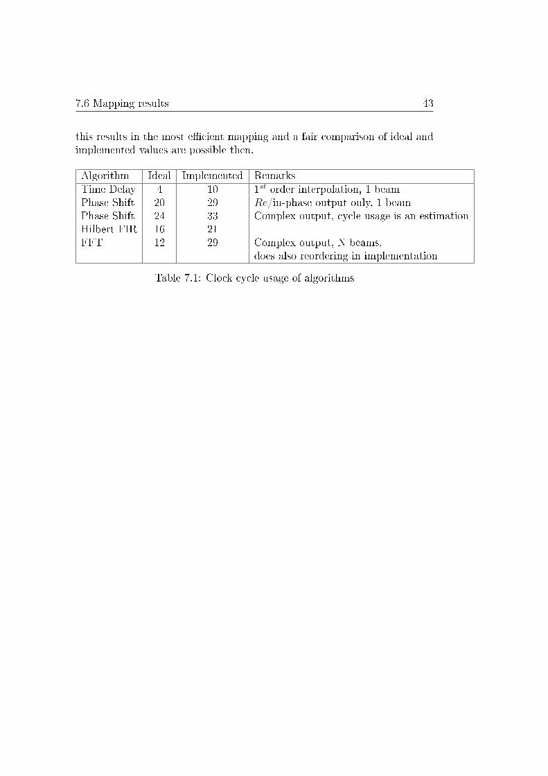
7.6 Mapping results 43
this results in the most e�cient mapping and a fair comparison of ideal andimplemented values are possible then.
Algorithm Ideal Implemented RemarksTime Delay 4 10 1st order interpolation, 1 beamPhase Shift 20 29 Re/in-phase output only, 1 beamPhase Shift 24 33 Complex output, cycle usage is an estimationHilbert FIR 16 21FFT 12 29 Complex output, N beams,
does also reordering in implementation
Table 7.1: Clock cycle usage of algorithms

44 Mapping beam forming algorithms to recon�gurable hardware
Chapter 8
Applications
A beam former can be designed for di�erent application purposes. Forthese di�erent purposes, the design parameters di�ers considerably. First anoverview of di�erent Montium implementations with their operation speedwill be given. Then a number of possible scenarios are given in which beamforming can be applied.
8.1 Montium processing throughput
The current Montium implementation on the BCVP1 reaches clock speedsof around 6 MHz. For some applications mentioned in this chapter this isnot su�cient high. In the Annabelle2 chip clock speed of 25 MHz (worstcase) to 100 MHz (best case) are reached. For this chip a 100 MHz Montiumclock speed will be assumed. A future implementation of the Montium withpipelining could reach clock speeds till 500 MHz, this is hyphotetical. Thecurrent Montium features east-west connections which spread throughout 5ALU's. In chip design, such long combinational paths slow down maximumclock speeds. In an improved design of the Montium, which handles theseconnections otherwise, such higher clock speed can be expected.
A Montium features 5 ALUs which can do 1 MAC/ALU. With theseimplementations a throughput in Million Multiply Accumulate (MMAC) in-structions per second is given, in platforms with multiple Montiums, the totalthroughput in MMAC is given:
1BCVP is a �rst generation concept validation platform and houses three Montiums2Annabelle is equipped with four second generation Montiums
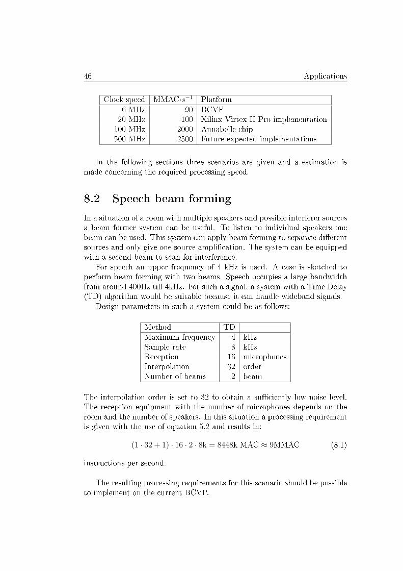
46 Applications
Clock speed MMAC·s−1 Platform6 MHz 90 BCVP20 MHz 100 Xilinx Virtex II Pro implementation100 MHz 2000 Annabelle chip500 MHz 2500 Future expected implementations
In the following sections three scenarios are given and a estimation ismade concerning the required processing speed.
8.2 Speech beam forming
In a situation of a room with multiple speakers and possible interferer sourcesa beam former system can be useful. To listen to individual speakers onebeam can be used. This system can apply beam forming to separate di�erentsources and only give one source ampli�cation. The system can be equippedwith a second beam to scan for interference.
For speech an upper frequency of 4 kHz is used. A case is sketched toperform beam forming with two beams. Speech occupies a large bandwidthfrom around 400Hz till 4kHz. For such a signal, a system with a Time Delay(TD) algorithm would be suitable because it can handle wideband signals.
Design parameters in such a system could be as follows:
Method TDMaximum frequency 4 kHzSample rate 8 kHzReception 16 microphonesInterpolation 32 orderNumber of beams 2 beam
The interpolation order is set to 32 to obtain a su�ciently low noise level.The reception equipment with the number of microphones depends on theroom and the number of speakers. In this situation a processing requirementis given with the use of equation 5.2 and results in:
(1 · 32 + 1) · 16 · 2 · 8k = 8448k MAC ≈ 9MMAC (8.1)
instructions per second.
The resulting processing requirements for this scenario should be possibleto implement on the current BCVP.
8.3 Quality audio beam forming 47
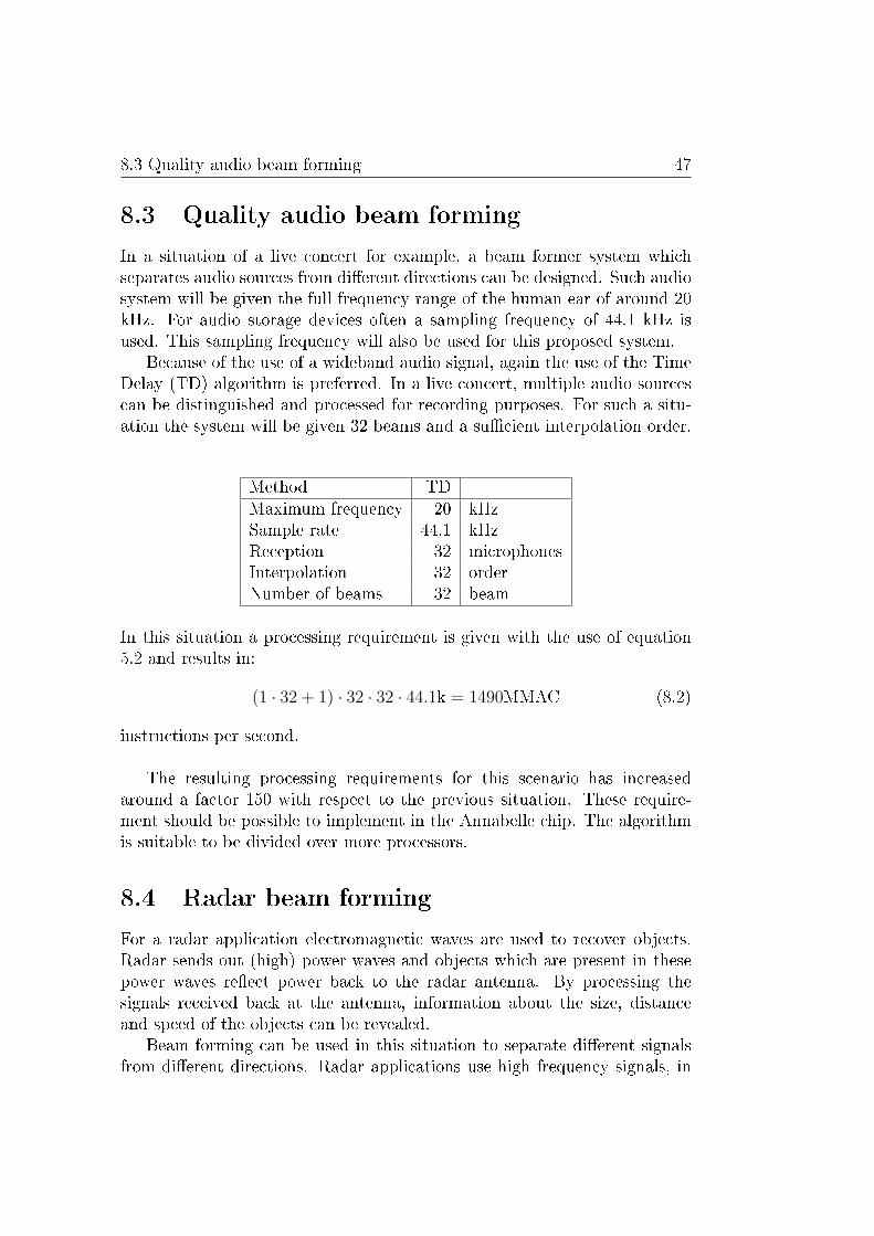
8.3 Quality audio beam forming
In a situation of a live concert for example, a beam former system whichseparates audio sources from di�erent directions can be designed. Such audiosystem will be given the full frequency range of the human ear of around 20kHz. For audio storage devices often a sampling frequency of 44.1 kHz isused. This sampling frequency will also be used for this proposed system.
Because of the use of a wideband audio signal, again the use of the TimeDelay (TD) algorithm is preferred. In a live concert, multiple audio sourcescan be distinguished and processed for recording purposes. For such a situ-ation the system will be given 32 beams and a su�cient interpolation order.
Method TDMaximum frequency 20 kHzSample rate 44.1 kHzReception 32 microphonesInterpolation 32 orderNumber of beams 32 beam
In this situation a processing requirement is given with the use of equation5.2 and results in:
(1 · 32 + 1) · 32 · 32 · 44.1k = 1490MMAC (8.2)
instructions per second.
The resulting processing requirements for this scenario has increasedaround a factor 150 with respect to the previous situation. These require-ment should be possible to implement in the Annabelle chip. The algorithmis suitable to be divided over more processors.
8.4 Radar beam forming
For a radar application electromagnetic waves are used to recover objects.Radar sends out (high) power waves and objects which are present in thesepower waves re�ect power back to the radar antenna. By processing thesignals received back at the antenna, information about the size, distanceand speed of the objects can be revealed.
Beam forming can be used in this situation to separate di�erent signalsfrom di�erent directions. Radar applications use high frequency signals, in
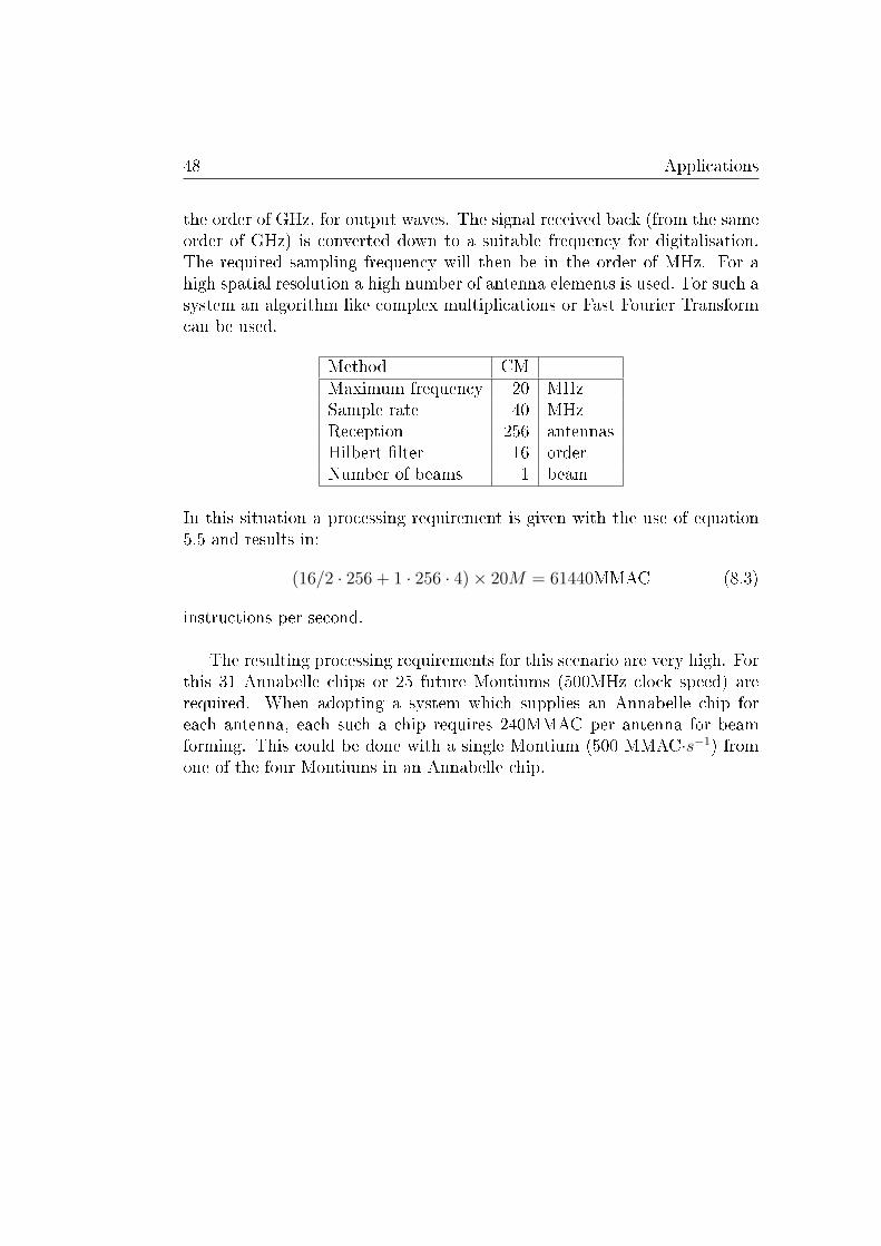
48 Applications
the order of GHz, for output waves. The signal received back (from the sameorder of GHz) is converted down to a suitable frequency for digitalisation.The required sampling frequency will then be in the order of MHz. For ahigh spatial resolution a high number of antenna elements is used. For such asystem an algorithm like complex multiplications or Fast Fourier Transformcan be used.
Method CMMaximum frequency 20 MHzSample rate 40 MHzReception 256 antennasHilbert �lter 16 orderNumber of beams 1 beam
In this situation a processing requirement is given with the use of equation5.5 and results in:
(16/2 · 256 + 1 · 256 · 4)× 20M = 61440MMAC (8.3)
instructions per second.
The resulting processing requirements for this scenario are very high. Forthis 31 Annabelle chips or 25 future Montiums (500MHz clock speed) arerequired. When adopting a system which supplies an Annabelle chip foreach antenna, each such a chip requires 240MMAC per antenna for beamforming. This could be done with a single Montium (500 MMAC·s−1) fromone of the four Montiums in an Annabelle chip.
Chapter 9
Conclusion and Recommendations
9.1 Conclusion
Di�erent mathematical methods are suitable for implementation on digitalprocessors. The Montium processor is used in the veri�cations of these algo-rithms and can be con�gured e�ciently. The implementation on the Xilinxdevelopment board shows that the Montium processor can apply these al-gorithms in real-time in an actual system. The Montium in a single setupperforms well for audio applications. Also an advantage is that the algo-rithms do not use complex branch instructions but are mainly forward �ltercalculations.
In the Complex Multiplication method the Hilbert �lter was originallynot predicted. This extra �lter greatly increases the amount of processingrequired by digital processors.
In chapter 8, the scenario of a radar beam former is described. Thisscenario puts high requirements for a beam former. Because of the lowspeed of the Montium, multiple processors are needed. For radar designs thecurrent implementation of the Montium can be used for beam forming. Asystem with multiple cores or chips is suitable for processing.
The Montium's full design features a logic function array in its ALUs.This logic function array is currently not used in the methods of Time Delayor Complex Multiplications. The FFT method can use scaling in betweendi�erent stages, this scaling is done with the use of the logic function array.The Montium can be adapted for speci�c purposes, in applications whereno FFT processing is needed the logic function array can be left out of thedesign. This could save space in a �nal design.
50 Conclusion and Recommendations
9.2 Recommendations
9.2.1 Partial recon�guration
The Montium is currently programmed with complete sets of con�gurationcode. When the processing is switched to another algorithm the completeprogram memory is rewritten. The Montium also has the option for partialrecon�guration [15], which could be used to switch faster between di�erentalgorithms.
The option of partial recon�guration also makes another change possible.For the Time Delay method, beam steering delay parameters and interpo-lation coe�cients are in registers. Updating these coe�cients takes two ad-ditions on the ALU at this moment. The coe�cients are stored in registersto support multiple channels on one processing part. When these delay pa-rameters are moved to the Montium AGUs, the AGU can take care of theadditions and saves two clock cycles. In this new situation, the Montium willneed to be recon�gured, by a master, with new coe�cients.
9.2.2 Scalability
For high demanding beam forming applications and the possibility to supportfurther post-processing a system with a lot of computational power is needed.Within the CRISP project a chip with 64 Montium will be developed. In thedesign of such a chip, to be suitable for a radar beam forming application,it will have to provide high speed input/output and interconnect, as well ashigh speed inter-processor connections.
The speed of the processors in such a chip should be suitable for highspeed computations. A speedup of the current Montium clock is preferredabove the possibility to be able to use the current east-west connections ofthe Montium ALUs. The east-west connections are not often used in theimplementation. This can be a starting place for optimization.
Bibliography
[1] Skolnik, M.I., Introduction to Radar Systems, 3rd ed. New York:McGraw-Hill, 2001
[2] Visser, Hubregt J., Array and Phased Array antenna basics, JohnWiley & Sons, Chichester, 2005
[3] Godara, Lal Chand, Smart Antennas, Boca Raton: CRC Press,2004
[4] Paul M. Heysters, Coarse-Grained Recon�gurable Processors, Flex-ibility meets E�ciency, Ph.D Thesis, 2004
[5] Recore Systems, P.O. Box 77, 7500AB Enschede, The Netherlands
[6] J.G. bij de Vaate, S.J. Wijnholds and J.D. Bregman, TwoDimensional 256 Element Phased Array System for Radio Astron-omy, Technical report, www.astron.nl/tl/thea/publications, Astron, TheNetherlands
[7] C. Alakija and S.P. Stapleton, A Mobile Base Station PhasedArray Antenna, Simon Fraser University, Canada, IEEE Wireless Com-munications, June 1992
[8] I. Chiba, R. Miura, T. Tanaka and Y. Karasawa, Digital BeamForming Antenna System for Mobile Communications, IEEE AES Sys-tems Magazine, September 1997
[9] T. Gebauer, H.G. Göckler, Channel-individual Adaptive Beam-forming for Mobile Satellite Communications, IEEE Journal, Vol. 13No. 2, February 1995
[10] L. Zhuang, C.G.H. Roeloffzen, R.G. Heideman, A. Borreman,A. Meijerink, and W.C. van Etten, Single-chip optical beam form-ing network in LPCVD waveguide technology based on optical ring res-
52 BIBLIOGRAPHY
onators, Proceedings of International Topical Meeting on MicrowavePhotonics (MWP'2006), IEEE France F1.4., Oct 2006
[11] P. Barton, Digital Beam Forming of Radar, IEE Proc. 127 No. 4,August 1980
[12] www.complextoreal.com,
[13] Advanced Telecommunications Research Institute International (ATR),2-2 Hikaridai, Kyoto 619-02, Japan
[14] Albert Molderink, Mapping FIR �lters on a Montium, Technicalreport, University of Twente, 2006
[15] MSc. K.H.G. Walters, Cognitive Radio on a recon�gurable platform,M.Sc. thesis, University of Twente, 2007
[16] Xilinx, EDK Base System Builder (BSB) support for XUPV2P Board,Xilinx (2005), www.xilinx.com
[17] Xilinx, Xilinx University Program Virtex-II Pro Development System,Hardware Reference Manual, Xilinx (2005), www.xilinx.com
[18] xilinx, Embedded System Tools Reference Manual, Embedded Devel-opment Kit EDK 8.1i, Xilinx (2005), www.xilinx.com
[19] National Semiconductors, DatasheetADCS7476/ADCS7477/ADCS7478, National Semiconductors (2007),www.national.com
[20] M.D. van de Burgwal, Hydra Protocol Speci�cation, Technicalreport, University of Twente (2007).
[21] Recore, Simsation Compiler Getting Started Guide, Recore (2007)
[22] Recore, Simsation Simulator Quick Reference Guide, Recore (2007)
List of Figures
1.1 Schematic representation of a line antenna array, top view . . 21.2 Total system with processing stages . . . . . . . . . . . . . . . 3
4.1 Schematic representation of two array elements with a wavefront 134.2 Response of phased array processing using �t processing, angle
of -90 to 90 degrees in 16 steps . . . . . . . . . . . . . . . . . . 154.3 Response of an phase array antenna with 4 (red), 16 (blue) and
64 (green) antennas, using complex multiplication to performbeam forming . . . . . . . . . . . . . . . . . . . . . . . . . . . 15
5.1 Schematic of signal �ow with time delay using bu�ers andinterpolating . . . . . . . . . . . . . . . . . . . . . . . . . . . . 20
5.2 Impuls response of linear interpolation (blue) and an idealsinc(x) interpolation (red) . . . . . . . . . . . . . . . . . . . . 21
5.3 Frequency response of linear interpolation (blue), an idealsinc(x) interpolation (red), a 32th order approximation (green)and a 64th order approximation (black) . . . . . . . . . . . . 21
5.4 Response of an phase array antenna with time delay, beamdirection of arrival 45 degrees . . . . . . . . . . . . . . . . . . 23
5.5 Impulse response of a Hilbert �lter . . . . . . . . . . . . . . . 255.6 Frequency response of a Hilbert FIR �lter . . . . . . . . . . . 265.7 Schematic signal �ow with complex multiplication . . . . . . . 275.8 Schematic signal �ow with FFT processing . . . . . . . . . . . 295.9 Computational complexity of di�erent algorithms with respect
to number of antennas. For complex multiplication processingand FFT processing a Hilbert �lter of 16th order is used. . . . 30
6.1 Hardware design of the testplatform . . . . . . . . . . . . . . . 336.2 Data �ow of a single stage (Time Delay or Phase Shift) process 346.3 Data �ow of a double stage (Hilbert and FFT) process . . . . 34
7.1 Memory and ALU register mapping . . . . . . . . . . . . . . . 37
54 LIST OF FIGURES
7.2 Memory and ALU register mapping . . . . . . . . . . . . . . . 417.3 Response of an beam former implementation with Complex
Multiplications . . . . . . . . . . . . . . . . . . . . . . . . . . 42
A.1 ADC module . . . . . . . . . . . . . . . . . . . . . . . . . . . 55A.2 Communication signals between ADC and development board 57
C.1 An instantiation of the Chameleon template . . . . . . . . . . 74C.2 The Montium tile including Hydra . . . . . . . . . . . . . . . 75C.3 An ALU of the Montium. The functional units are all capable
of various logical operations. For a complete listing pleaserefer to [4] . . . . . . . . . . . . . . . . . . . . . . . . . . . . . 77
Appendix A
VHDL ADC interface design
The used analog digital converters are from Digilent Inc, modules PMOD-AD1. These modules features two 12 bit ADC with �ltering and a 1 MSpssampling frequency. They are equipped with the ADC chips from NationalSemiconductors type ADCS7476. A picture and electrical diagram are shownin �gure A.1.
The chips use a serial communication interface, which is not provided inthe standard Xilinx development software. Therefore an interface is madeseparately as a VHDL module. This interface is connected to the OPB busand uses the OPB clock of 10MHz to create a bit-clock and a sample-clockfor the ADC's.
(a) Picture (b) Electrical block dia-gram
Figure A.1: ADC module
The modules are connected with the use of a module interface board(MIB), this interface board is connected to the low speed expansion header0 of the development board. The interface board has 8 6-pin connections, oneach such connection an ADC module can be connected.
56 VHDL ADC interface design
ADC protocol
The interface consists of four signal lines, the ADC is driven with a sampleclock which initiates a sample/hold and conversion. The bit-clock is thenused to clock the output of the di�erent bits. 16 bits are transmitted the�rst 4 are leading zeros, the bits following is the sampled value. The pinningof the ADC modules is shown in table A.2. The protocol is veri�ed with theuse of a logic analyzer/digital scope (Rigol, DS 1102CD). The signal �owof two channels is recorded for 2 samples times, this is shown in �gure A.2,consult table A.2 to recover the corresponding meaning of signal pins.
Memory interface
The VHDL interfaces with the OPB bus, in the hardware design the interfaceis given a base address. The interaction with the OPB is memory mapped.The mapping of di�erent registers is shown in table A.1. The interface isfree-running and is clocked from the OPB bus. Samples are in registers andare read out with a leading 0x50.00.0 or a leading 0x51.00.0 for hardwarechannel 0 or 1 respectively.
Channel O�set addr. MIB Data format1 4 1 0x50.00.0v.vv2 8 1 0x51.00.0v.vv3 12 2 0x50.00.0v.vv4 16 2 0x51.00.0v.vv5 20 3 0x50.00.0v.vv6 24 3 0x51.00.0v.vv7 28 4 0x50.00.0v.vv8 32 4 0x51.00.0v.vv15 56 8 0x50.00.0v.vv16 60 8 0x51.00.0v.vvSattus reg. 64 - 0xAB.CD.xx.yy
Table A.1: Memory mapping of the interface, v.vv represent a 12 bits sampledvalue, xx and yy the status bits of channel 0 and 1.
57
Pin Male/Digital Conn. Direction DescriptionSample clock 1 I Shown in �gure A.2 as �D4�Data line 0 2 O Shown in �gure A.2 as �D3�Data line 1 3 O Shown in �gure A.2 as �D2�Bit clock 4 I Shown in �gure A.2 as �D1�Ground 5 IVCC 6 I 3.3 Power supply from dev. boardPin Female/Analog Conn. Direction DescriptionAnalog inp 0 1 IAnalog inp 1 3 IGround 2,4,5 I/OVCC 6 O
Table A.2: Hardware pin description of the ADC module
Figure A.2: Communication signals between ADC and development board

58 VHDL ADC interface design
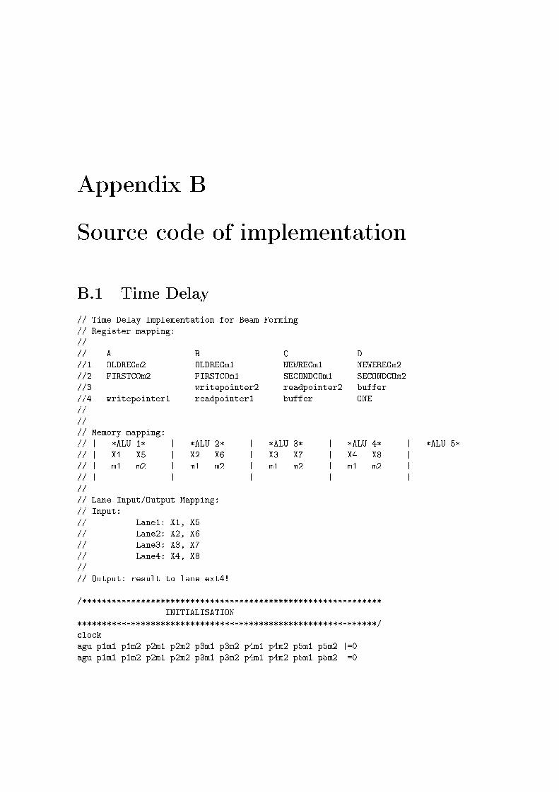
Appendix B
Source code of implementation
B.1 Time Delay
// Time Delay Implementation for Beam Forming
// Register mapping:
//
// A B C D
//1 OLDREGm2 OLDREGm1 NEWREGm1 NEWEREGm2
//2 FIRSTCOm2 FIRSTCOm1 SECONDCOm1 SECONDCOm2
//3 writepointer2 readpointer2 buffer
//4 writepointer1 readpointer1 buffer ONE
//
//
// Memory mapping:
// | *ALU 1* | *ALU 2* | *ALU 3* | *ALU 4* | *ALU 5*
// | X1 X5 | X2 X6 | X3 X7 | X4 X8 |
// | m1 m2 | m1 m2 | m1 m2 | m1 m2 |
// | | | | |
//
// Lane Input/Output Mapping:
// Input:
// Lane1: X1, X5
// Lane2: X2, X6
// Lane3: X3, X7
// Lane4: X4, X8
//
// Output: result to lane ext4!
/*************************************************************
INITIALISATION
*************************************************************/
clock
agu p1m1 p1m2 p2m1 p2m2 p3m1 p3m2 p4m1 p4m2 p5m1 p5m2 |=0
agu p1m1 p1m2 p2m1 p2m2 p3m1 p3m2 p4m1 p4m2 p5m1 p5m2 =0
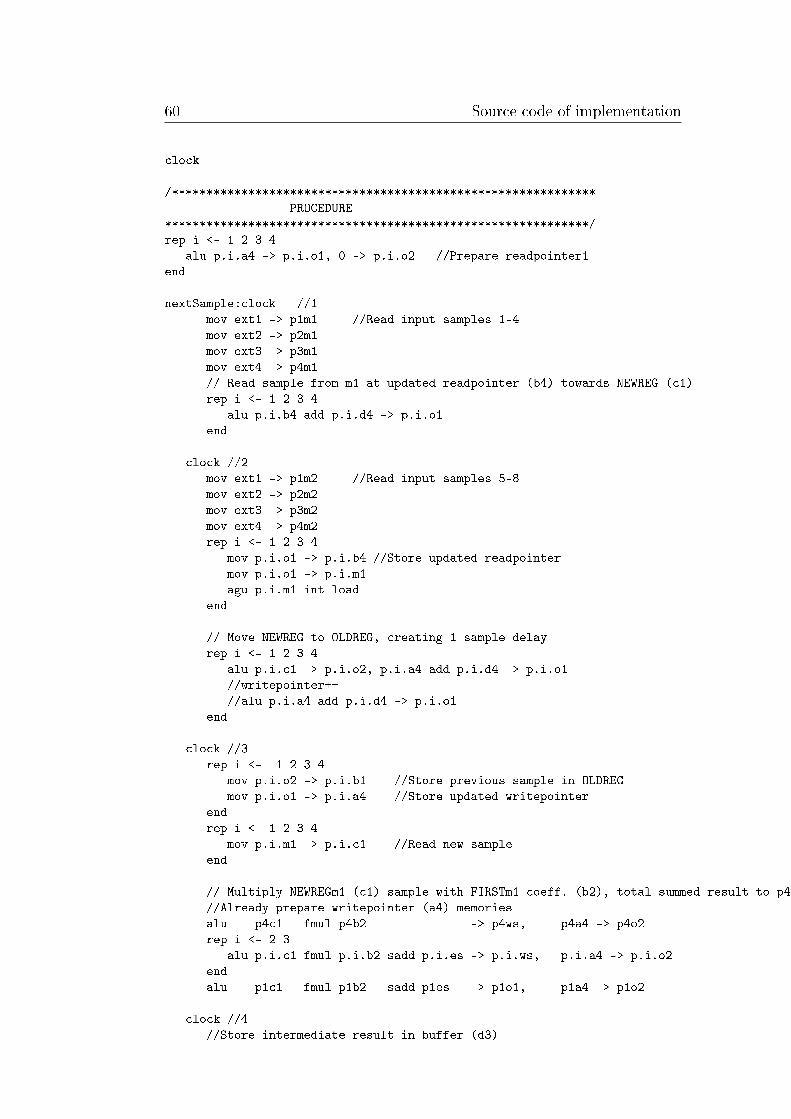
60 Source code of implementation
clock
/*************************************************************
PROCEDURE
*************************************************************/
rep i <- 1 2 3 4
alu p.i.a4 -> p.i.o1, 0 -> p.i.o2 //Prepare readpointer1
end
nextSample:clock //1
mov ext1 -> p1m1 //Read input samples 1-4
mov ext2 -> p2m1
mov ext3 -> p3m1
mov ext4 -> p4m1
// Read sample from m1 at updated readpointer (b4) towards NEWREG (c1)
rep i <- 1 2 3 4
alu p.i.b4 add p.i.d4 -> p.i.o1
end
clock //2
mov ext1 -> p1m2 //Read input samples 5-8
mov ext2 -> p2m2
mov ext3 -> p3m2
mov ext4 -> p4m2
rep i <- 1 2 3 4
mov p.i.o1 -> p.i.b4 //Store updated readpointer
mov p.i.o1 -> p.i.m1
agu p.i.m1 int load
end
// Move NEWREG to OLDREG, creating 1 sample delay
rep i <- 1 2 3 4
alu p.i.c1 -> p.i.o2, p.i.a4 add p.i.d4 -> p.i.o1
//writepointer++
//alu p.i.a4 add p.i.d4 -> p.i.o1
end
clock //3
rep i <- 1 2 3 4
mov p.i.o2 -> p.i.b1 //Store previous sample in OLDREG
mov p.i.o1 -> p.i.a4 //Store updated writepointer
end
rep i <- 1 2 3 4
mov p.i.m1 -> p.i.c1 //Read new sample
end
// Multiply NEWREGm1 (c1) sample with FIRSTm1 coeff. (b2), total summed result to p4d1
//Already prepare writepointer (a4) memories
alu p4c1 fmul p4b2 -> p4ws, p4a4 -> p4o2
rep i <- 2 3
alu p.i.c1 fmul p.i.b2 sadd p.i.es -> p.i.ws, p.i.a4 -> p.i.o2
end
alu p1c1 fmul p1b2 sadd p1es -> p1o1, p1a4 -> p1o2
clock //4
//Store intermediate result in buffer (d3)
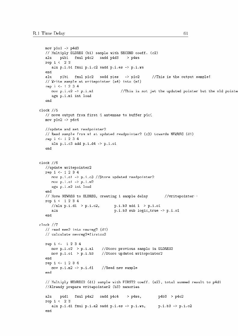
B.1 Time Delay 61
mov p1o1 -> p4d3
// Multiply OLDREG (b1) sample with SECOND coeff. (c2)
alu p4b1 fmul p4c2 sadd p4d3 -> p4ws
rep i <- 2 3
alu p.i.b1 fmul p.i.c2 sadd p.i.es -> p.i.ws
end
alu p1b1 fmul p1c2 sadd p1es -> p1o2 //This is the output sample!
// Write sample at writepointer (a4) into (m1)
rep i <- 1 2 3 4
mov p.i.o2 -> p.i.m1 //This is not jet the updated pointer but the old pointer
agu p.i.m1 int load
end
clock //5
// move output from first 4 antennas to buffer p4c4
mov p1o2 -> p4c4
//update and set readpointer2
// Read sample from m1 at updated readpointer2 (c3) towards NEWREG (d1)
rep i <- 1 2 3 4
alu p.i.c3 add p.i.d4 -> p.i.o1
end
clock //6
//update writepointer2
rep i <- 1 2 3 4
mov p.i.o1 -> p.i.c3 //Store updated readpointer2
mov p.i.o1 -> p.i.m2
agu p.i.m2 int load
end
// Move NEWREG to OLDREG, creating 1 sample delay //writepointer++
rep i <- 1 2 3 4
//alu p.i.d1 -> p.i.o2, p.i.b3 add 1 -> p.i.o1
alu p.i.b3 sub logic_true -> p.i.o1
end
clock //7
// read mem2 into newreg2 (d1)
// calculate newreg2*firstco2
rep i <- 1 2 3 4
mov p.i.o2 -> p.i.a1 //Store previous sample in OLDREG2
mov p.i.o1 -> p.i.b3 //Store updated writepointer2
end
rep i <- 1 2 3 4
mov p.i.m2 -> p.i.d1 //Read new sample
end
// Multiply NEWREG2 (d1) sample with FIRST2 coeff. (a2), total summed result to p4d1
//Already prepare writepointer2 (b3) memories
alu p4d1 fmul p4a2 sadd p4c4 -> p4ws, p4b3 -> p4o2
rep i <- 2 3
alu p.i.d1 fmul p.i.a2 sadd p.i.es -> p.i.ws, p.i.b3 -> p.i.o2
end
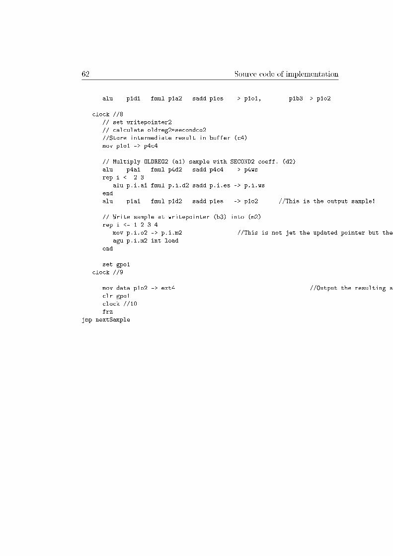
62 Source code of implementation
alu p1d1 fmul p1a2 sadd p1es -> p1o1, p1b3 -> p1o2
clock //8
// set writepointer2
// calculate oldreg2*secondco2
//Store intermediate result in buffer (c4)
mov p1o1 -> p4c4
// Multiply OLDREG2 (a1) sample with SECOND2 coeff. (d2)
alu p4a1 fmul p4d2 sadd p4c4 -> p4ws
rep i <- 2 3
alu p.i.a1 fmul p.i.d2 sadd p.i.es -> p.i.ws
end
alu p1a1 fmul p1d2 sadd p1es -> p1o2 //This is the output sample!
// Write sample at writepointer (b3) into (m2)
rep i <- 1 2 3 4
mov p.i.o2 -> p.i.m2 //This is not jet the updated pointer but the old pointer
agu p.i.m2 int load
end
set gpo1
clock //9
mov data p1o2 -> ext4 //Output the resulting sample!!!
clr gpo1
clock //10
frz
jmp nextSample
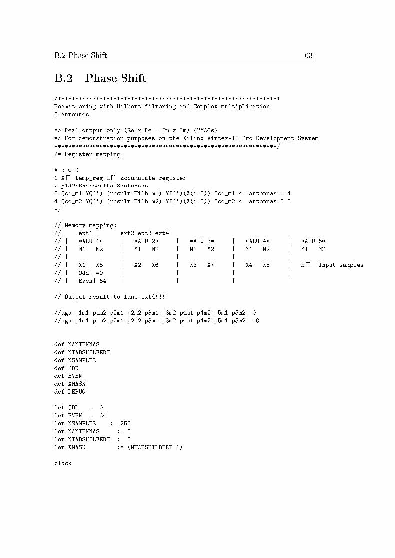
B.2 Phase Shift 63
B.2 Phase Shift
/****************************************************************
Beamsteering with Hilbert filtering and Complex multiplication
8 antennes
=> Real output only (Re x Re + Im x Im) (2MACs)
=> For demonstration purposes on the Xilinx Virtex-II Pro Development System
****************************************************************/
/* Register mapping:
A B C D
1 X[] temp_reg H[] accumulate register
2 p1d2:Endresultof8antennas
3 Qco_m1 YQ(i) (result Hilb m1) YI(i)(X(i-5)) Ico_m1 <= antennas 1-4
4 Qco_m2 YQ(i) (result Hilb m2) YI(i)(X(i-5)) Ico_m2 <= antennas 5-8
*/
// Memory mapping:
// ext1 ext2 ext3 ext4
// | *ALU 1* | *ALU 2* | *ALU 3* | *ALU 4* | *ALU 5*
// | M1 M2 | M1 M2 | M1 M2 | M1 M2 | M1 M2
// | | | | |
// | X1 X5 | X2 X6 | X3 X7 | X4 X8 | H[] Input samples
// | Odd |=0 | | | |
// | Even|=64 | | | |
// Output result to lane ext4!!!
//agu p1m1 p1m2 p2m1 p2m2 p3m1 p3m2 p4m1 p4m2 p5m1 p5m2 =0
//agu p1m1 p1m2 p2m1 p2m2 p3m1 p3m2 p4m1 p4m2 p5m1 p5m2 |=0
def NANTENNAS
def NTABSHILBERT
def NSAMPLES
def ODD
def EVEN
def XMASK
def DEBUG
let ODD := 0
let EVEN := 64
let NSAMPLES := 256
let NANTENNAS := 8
let NTABSHILBERT := 8
let XMASK := (NTABSHILBERT-1)
clock
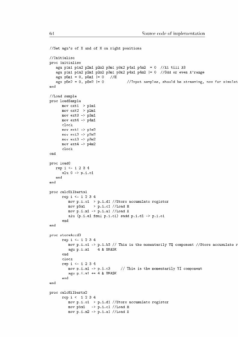
64 Source code of implementation
//Set agu's of X and of H on right positions
//Initialise
proc initialise
agu p1m1 p1m2 p2m1 p2m2 p3m1 p3m2 p4m1 p4m2 = 0 //X1 till X8
agu p1m1 p1m2 p2m1 p2m2 p3m1 p3m2 p4m1 p4m2 |= 0 //Odd or even X'range
agu p5m1 = 0, p5m1 |= 0 //H
agu p5m2 = 0, p5m2 |= 0 //Input samples, should be streaming, now for simulation purpose
end
//Load sample
proc loadSample
mov ext1 -> p1m1
mov ext2 -> p2m1
mov ext3 -> p3m1
mov ext4 -> p4m1
clock
mov ext1 -> p1m2
mov ext2 -> p2m2
mov ext3 -> p3m2
mov ext4 -> p4m2
clock
end
proc load0
rep i <- 1 2 3 4
alu 0 -> p.i.o1
end
end
proc calcHilbertm1
rep i <- 1 2 3 4
mov p.i.o1 -> p.i.d1 //Store accumulate register
mov p5m1 -> p.i.c1 //Load H
mov p.i.m1 -> p.i.a1 //Load X
alu (p.i.a1 fmul p.i.c1) sadd p.i.d1 -> p.i.o1
end
end
proc storeAccd3
rep i <- 1 2 3 4
mov p.i.o1 -> p.i.b3 // This is the momentarily YQ component //Store accumulate register
agu p.i.m1 -= 4 & XMASK
end
clock
rep i <- 1 2 3 4
mov p.i.m1 -> p.i.c3 // This is the momentarily YI component
agu p.i.m1 += 4 & XMASK
end
end
proc calcHilbertm2
rep i <- 1 2 3 4
mov p.i.o1 -> p.i.d1 //Store accumulate register
mov p5m1 -> p.i.c1 //Load H
mov p.i.m2 -> p.i.a1 //Load X
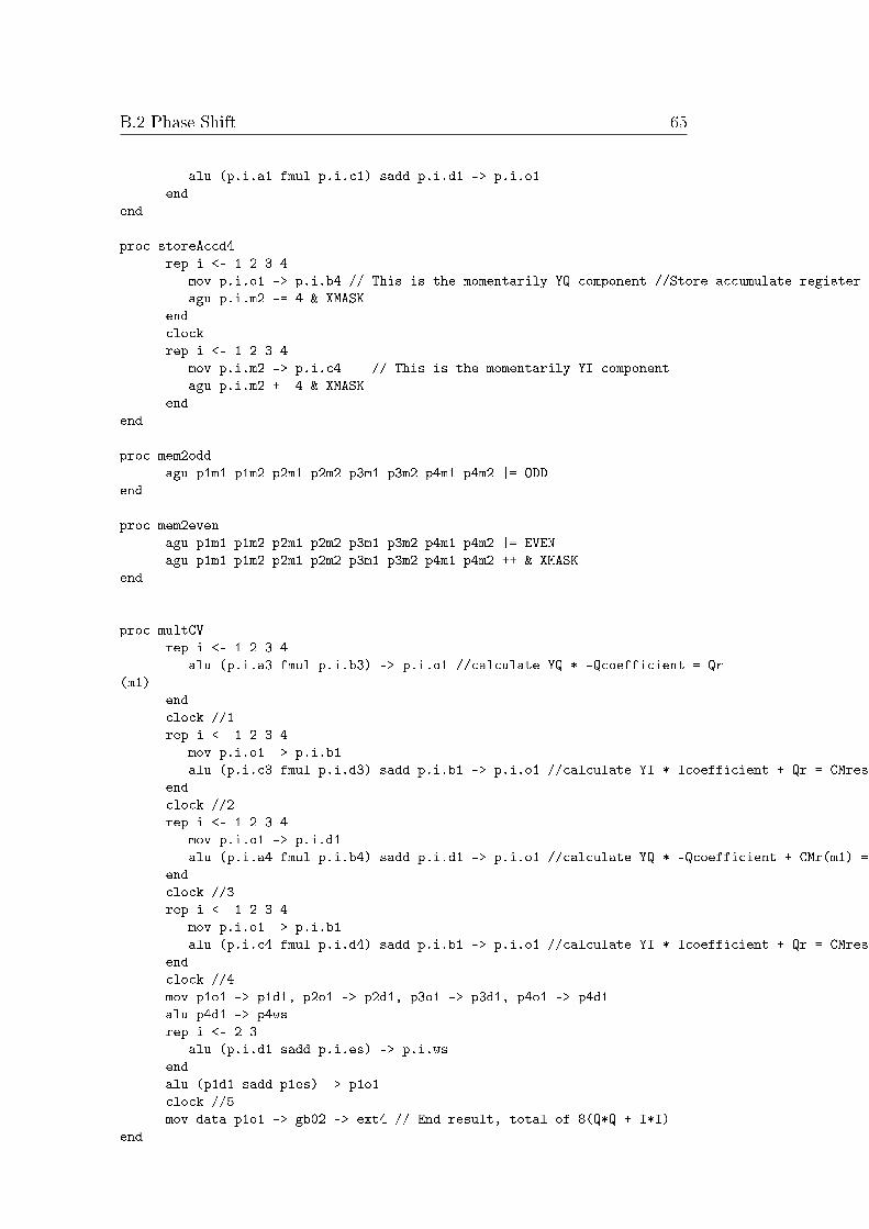
B.2 Phase Shift 65
alu (p.i.a1 fmul p.i.c1) sadd p.i.d1 -> p.i.o1
end
end
proc storeAccd4
rep i <- 1 2 3 4
mov p.i.o1 -> p.i.b4 // This is the momentarily YQ component //Store accumulate register
agu p.i.m2 -= 4 & XMASK
end
clock
rep i <- 1 2 3 4
mov p.i.m2 -> p.i.c4 // This is the momentarily YI component
agu p.i.m2 += 4 & XMASK
end
end
proc mem2odd
agu p1m1 p1m2 p2m1 p2m2 p3m1 p3m2 p4m1 p4m2 |= ODD
end
proc mem2even
agu p1m1 p1m2 p2m1 p2m2 p3m1 p3m2 p4m1 p4m2 |= EVEN
agu p1m1 p1m2 p2m1 p2m2 p3m1 p3m2 p4m1 p4m2 ++ & XMASK
end
proc multCV
rep i <- 1 2 3 4
alu (p.i.a3 fmul p.i.b3) -> p.i.o1 //calculate YQ * -Qcoefficient = Qr
(m1)
end
clock //1
rep i <- 1 2 3 4
mov p.i.o1 -> p.i.b1
alu (p.i.c3 fmul p.i.d3) sadd p.i.b1 -> p.i.o1 //calculate YI * Icoefficient + Qr = CMresult (m1)
end
clock //2
rep i <- 1 2 3 4
mov p.i.o1 -> p.i.d1
alu (p.i.a4 fmul p.i.b4) sadd p.i.d1 -> p.i.o1 //calculate YQ * -Qcoefficient + CMr(m1) = Qr (m2)
end
clock //3
rep i <- 1 2 3 4
mov p.i.o1 -> p.i.b1
alu (p.i.c4 fmul p.i.d4) sadd p.i.b1 -> p.i.o1 //calculate YI * Icoefficient + Qr = CMresult (m1)
end
clock //4
mov p1o1 -> p1d1, p2o1 -> p2d1, p3o1 -> p3d1, p4o1 -> p4d1
alu p4d1 -> p4ws
rep i <- 2 3
alu (p.i.d1 sadd p.i.es) -> p.i.ws
end
alu (p1d1 sadd p1es) -> p1o1
clock //5
mov data p1o1 -> gb02 -> ext4 // End result, total of 8(Q*Q + I*I)
end
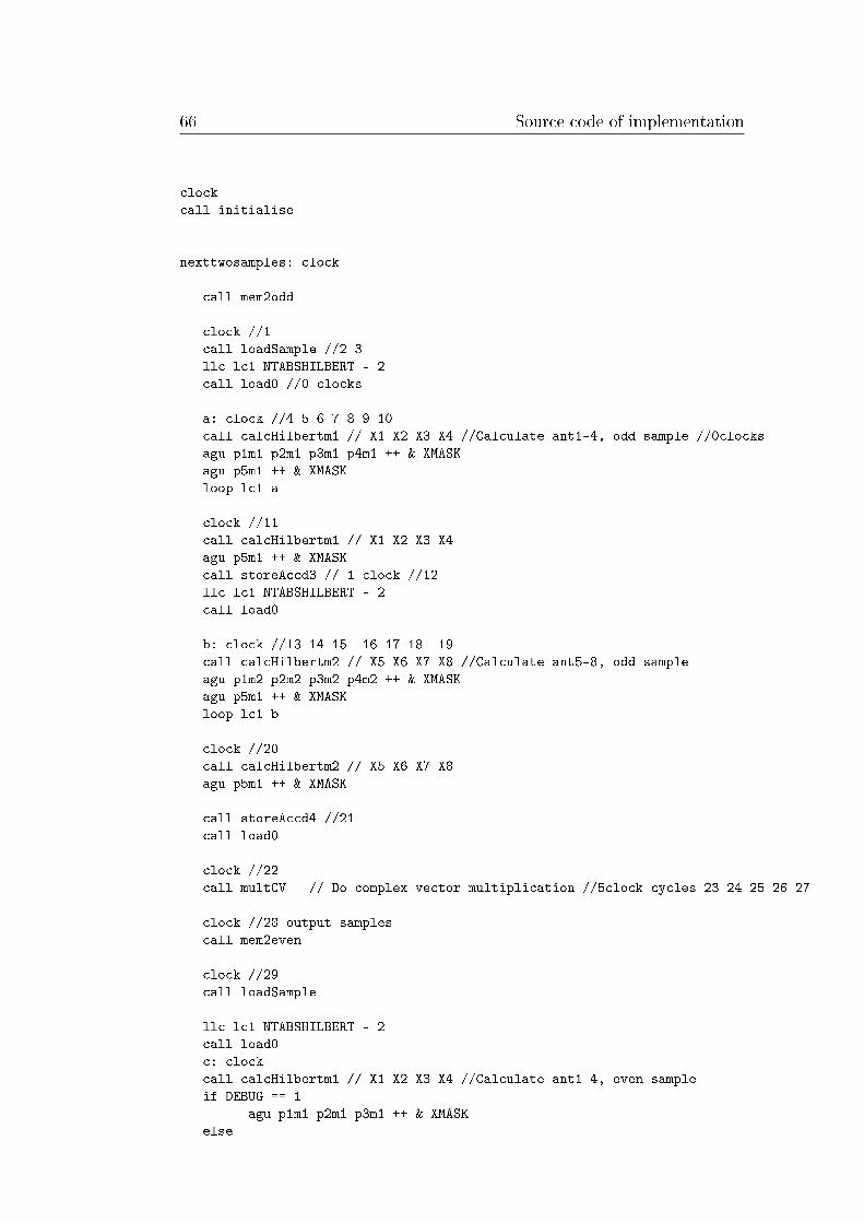
66 Source code of implementation
clock
call initialise
nexttwosamples: clock
call mem2odd
clock //1
call loadSample //2 3
llc lc1 NTABSHILBERT - 2
call load0 //0 clocks
a: clock //4 5 6 7 8 9 10
call calcHilbertm1 // X1 X2 X3 X4 //Calculate ant1-4, odd sample //0clocks
agu p1m1 p2m1 p3m1 p4m1 ++ & XMASK
agu p5m1 ++ & XMASK
loop lc1 a
clock //11
call calcHilbertm1 // X1 X2 X3 X4
agu p5m1 ++ & XMASK
call storeAccd3 // 1 clock //12
llc lc1 NTABSHILBERT - 2
call load0
b: clock //13 14 15 16 17 18 19
call calcHilbertm2 // X5 X6 X7 X8 //Calculate ant5-8, odd sample
agu p1m2 p2m2 p3m2 p4m2 ++ & XMASK
agu p5m1 ++ & XMASK
loop lc1 b
clock //20
call calcHilbertm2 // X5 X6 X7 X8
agu p5m1 ++ & XMASK
call storeAccd4 //21
call load0
clock //22
call multCV // Do complex vector multiplication //5clock cycles 23 24 25 26 27
clock //28 output samples
call mem2even
clock //29
call loadSample
llc lc1 NTABSHILBERT - 2
call load0
c: clock
call calcHilbertm1 // X1 X2 X3 X4 //Calculate ant1-4, even sample
if DEBUG == 1
agu p1m1 p2m1 p3m1 ++ & XMASK
else
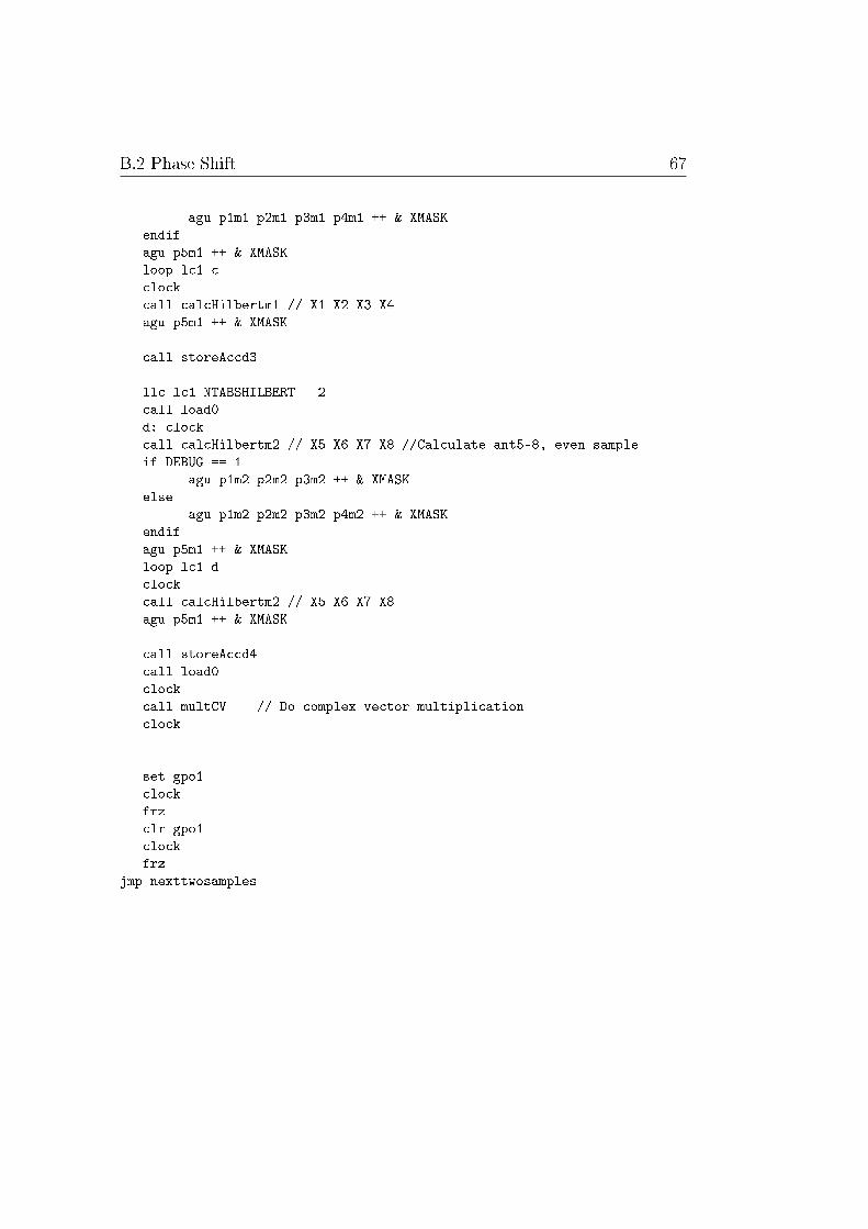
B.2 Phase Shift 67
agu p1m1 p2m1 p3m1 p4m1 ++ & XMASK
endif
agu p5m1 ++ & XMASK
loop lc1 c
clock
call calcHilbertm1 // X1 X2 X3 X4
agu p5m1 ++ & XMASK
call storeAccd3
llc lc1 NTABSHILBERT - 2
call load0
d: clock
call calcHilbertm2 // X5 X6 X7 X8 //Calculate ant5-8, even sample
if DEBUG == 1
agu p1m2 p2m2 p3m2 ++ & XMASK
else
agu p1m2 p2m2 p3m2 p4m2 ++ & XMASK
endif
agu p5m1 ++ & XMASK
loop lc1 d
clock
call calcHilbertm2 // X5 X6 X7 X8
agu p5m1 ++ & XMASK
call storeAccd4
call load0
clock
call multCV // Do complex vector multiplication
clock
set gpo1
clock
frz
clr gpo1
clock
frz
jmp nexttwosamples
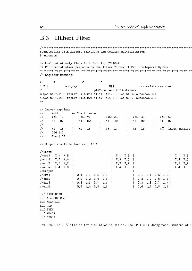
68 Source code of implementation
B.3 Hilbert Filter
/***************************************************************************************************************
Beamsteering with Hilbert filtering and Complex multiplication
8 antennes
=> Real output only (Re x Re + Im x Im) (2MACs)
=> For demonstration purposes on the Xilinx Virtex-II Pro Development System
***************************************************************************************************************/
/* Register mapping:
A B C D
1 X[] temp_reg H[] accumulate register
2 p1d2:Endresultof8antennas
3 Qco_m1 YQ(i) (result Hilb m1) YI(i) (X(i-5)) Ico_m1 <= antennas 1-4
4 Qco_m2 YQ(i) (result Hilb m2) YI(i) (X(i-5)) Ico_m2 <= antennas 5-8
*/
// Memory mapping:
// ext1 ext2 ext3 ext4
// | *ALU 1* | *ALU 2* | *ALU 3* | *ALU 4* | *ALU 5*
// | M1 M2 | M1 M2 | M1 M2 | M1 M2 | M1 M2
// | | | | |
// | X1 X5 | X2 X6 | X3 X7 | X4 X8 | H[] Input samples
// | Odd |=0 | | | |
// | Even|=64 | | | |
// Output result to lane ext1-4!!!
//Input
//ext1: X_1 X_5 | | X_1 X_5 | | X_1 X_5 |
//ext2: X_2 X_6 | | X_2 X_6 | | X_2 X_6 |
//ext3: X_3 X_7 | | X_3 X_7 | | X_3 X_7 |
//ext4: X_4 X_8 | | X_4 X_8 | | X_4 X_8 |
//Output: | | | | |
//ext1: | Q_1 I_1 Q_5 I_5 | | Q_1 I_1 Q_5 I_5 | | Q_1 I_1 Q_5 I_5
//ext2: | Q_2 I_2 Q_6 I_6 | | Q_2 I_2 Q_6 I_6 | | Q_2 I_2 Q_6 I_6
//ext3: | Q_3 I_3 Q_7 I_7 | | Q_3 I_3 Q_7 I_7 | | Q_3 I_3 Q_7 I_7
//ext4: | Q_4 I_4 Q_8 I_8 | | Q_4 I_4 Q_8 I_8 | | Q_4 I_4 Q_8 I_8
def NANTENNAS
def NTABSHILBERT
def NSAMPLES
def ODD
def EVEN
def XMASK
def DEBUG
let DEBUG := 0 // This is for simulation in Matlab, use PP 1-3 in debug mode, instead of 1-4
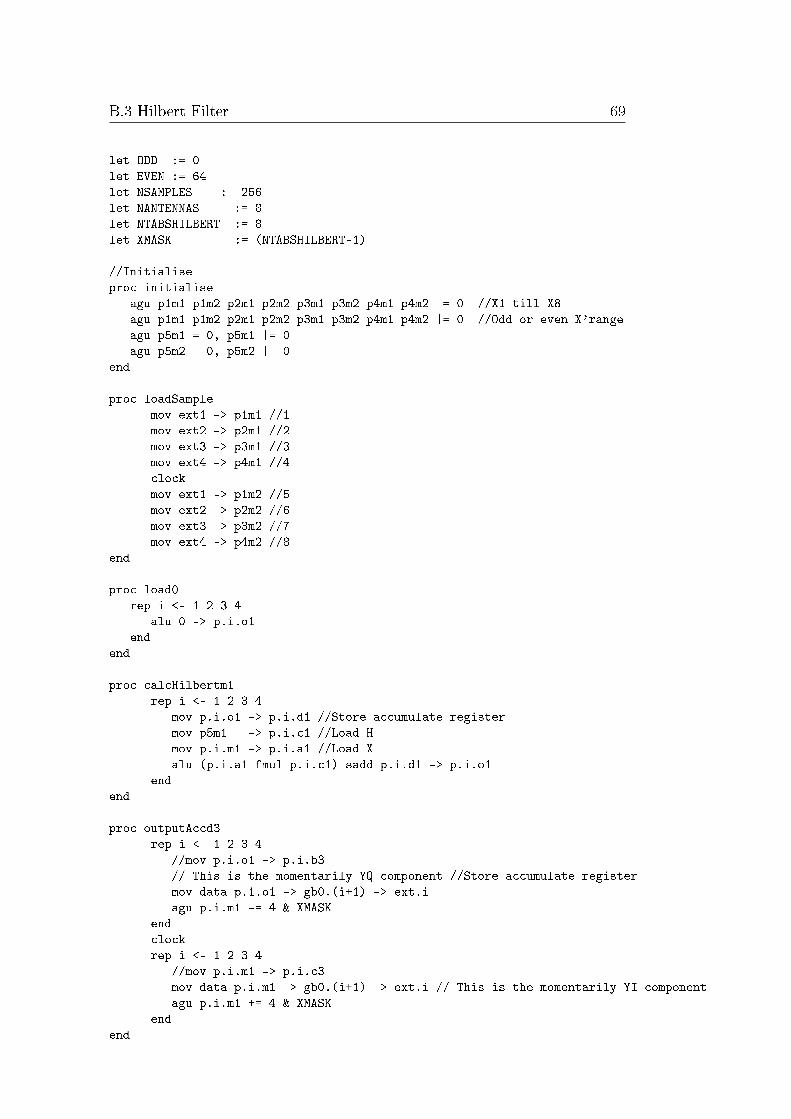
B.3 Hilbert Filter 69
let ODD := 0
let EVEN := 64
let NSAMPLES := 256
let NANTENNAS := 8
let NTABSHILBERT := 8
let XMASK := (NTABSHILBERT-1)
//Initialise
proc initialise
agu p1m1 p1m2 p2m1 p2m2 p3m1 p3m2 p4m1 p4m2 = 0 //X1 till X8
agu p1m1 p1m2 p2m1 p2m2 p3m1 p3m2 p4m1 p4m2 |= 0 //Odd or even X'range
agu p5m1 = 0, p5m1 |= 0
agu p5m2 = 0, p5m2 |= 0
end
proc loadSample
mov ext1 -> p1m1 //1
mov ext2 -> p2m1 //2
mov ext3 -> p3m1 //3
mov ext4 -> p4m1 //4
clock
mov ext1 -> p1m2 //5
mov ext2 -> p2m2 //6
mov ext3 -> p3m2 //7
mov ext4 -> p4m2 //8
end
proc load0
rep i <- 1 2 3 4
alu 0 -> p.i.o1
end
end
proc calcHilbertm1
rep i <- 1 2 3 4
mov p.i.o1 -> p.i.d1 //Store accumulate register
mov p5m1 -> p.i.c1 //Load H
mov p.i.m1 -> p.i.a1 //Load X
alu (p.i.a1 fmul p.i.c1) sadd p.i.d1 -> p.i.o1
end
end
proc outputAccd3
rep i <- 1 2 3 4
//mov p.i.o1 -> p.i.b3
// This is the momentarily YQ component //Store accumulate register
mov data p.1.o1 -> gb0.(i+1) -> ext.i
agu p.i.m1 -= 4 & XMASK
end
clock
rep i <- 1 2 3 4
//mov p.i.m1 -> p.i.c3
mov data p.i.m1 -> gb0.(i+1) -> ext.i // This is the momentarily YI component
agu p.i.m1 += 4 & XMASK
end
end
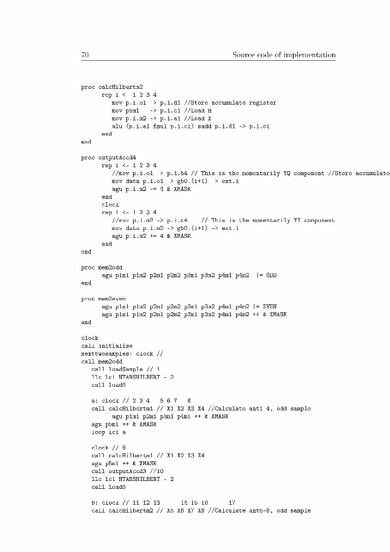
70 Source code of implementation
proc calcHilbertm2
rep i <- 1 2 3 4
mov p.i.o1 -> p.i.d1 //Store accumulate register
mov p5m1 -> p.i.c1 //Load H
mov p.i.m2 -> p.i.a1 //Load X
alu (p.i.a1 fmul p.i.c1) sadd p.i.d1 -> p.i.o1
end
end
proc outputAccd4
rep i <- 1 2 3 4
//mov p.i.o1 -> p.i.b4 // This is the momentarily YQ component //Store accumulate register
mov data p.i.o1 -> gb0.(i+1) -> ext.i
agu p.i.m2 -= 4 & XMASK
end
clock
rep i <- 1 2 3 4
//mov p.i.m2 -> p.i.c4 // This is the momentarily YI component
mov data p.i.m2 -> gb0.(i+1) -> ext.i
agu p.i.m2 += 4 & XMASK
end
end
proc mem2odd
agu p1m1 p1m2 p2m1 p2m2 p3m1 p3m2 p4m1 p4m2 |= ODD
end
proc mem2even
agu p1m1 p1m2 p2m1 p2m2 p3m1 p3m2 p4m1 p4m2 |= EVEN
agu p1m1 p1m2 p2m1 p2m2 p3m1 p3m2 p4m1 p4m2 ++ & XMASK
end
clock
call initialise
nexttwosamples: clock //
call mem2odd
call loadSample // 1
llc lc1 NTABSHILBERT - 2
call load0
a: clock // 2 3 4 5 6 7 8
call calcHilbertm1 // X1 X2 X3 X4 //Calculate ant1-4, odd sample
agu p1m1 p2m1 p3m1 p4m1 ++ & XMASK
agu p5m1 ++ & XMASK
loop lc1 a
clock // 9
call calcHilbertm1 // X1 X2 X3 X4
agu p5m1 ++ & XMASK
call outputAccd3 //10
llc lc1 NTABSHILBERT - 2
call load0
b: clock // 11 12 13 14 15 16 17
call calcHilbertm2 // X5 X6 X7 X8 //Calculate ant5-8, odd sample
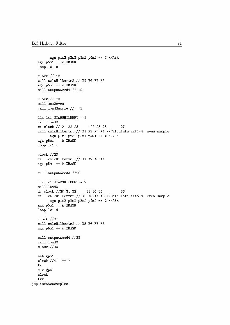
B.3 Hilbert Filter 71
agu p1m2 p2m2 p3m2 p4m2 ++ & XMASK
agu p5m1 ++ & XMASK
loop lc1 b
clock // 18
call calcHilbertm2 // X5 X6 X7 X8
agu p5m1 ++ & XMASK
call outputAccd4 // 19
clock // 20
call mem2even
call loadSample // ++1
llc lc1 NTABSHILBERT - 2
call load0
c: clock // 21 22 23 24 25 26 27
call calcHilbertm1 // X1 X2 X3 X4 //Calculate ant1-4, even sample
agu p1m1 p2m1 p3m1 p4m1 ++ & XMASK
agu p5m1 ++ & XMASK
loop lc1 c
clock //28
call calcHilbertm1 // X1 X2 X3 X4
agu p5m1 ++ & XMASK
call outputAccd3 //29
llc lc1 NTABSHILBERT - 2
call load0
d: clock //30 31 32 33 34 35 36
call calcHilbertm2 // X5 X6 X7 X8 //Calculate ant5-8, even sample
agu p1m2 p2m2 p3m2 p4m2 ++ & XMASK
agu p5m1 ++ & XMASK
loop lc1 d
clock //37
call calcHilbertm2 // X5 X6 X7 X8
agu p5m1 ++ & XMASK
call outputAccd4 //38
call load0
clock //39
set gpo1
clock //41 (++1)
frz
clr gpo1
clock
frz
jmp nexttwosamples

72 Source code of implementation
Appendix C
Montium tile processor
Here an explanation of the Montium tile processor is given. This chapter iscopied from the report of [15] with permission from the author.
C.1 Introduction
The Montium tile processor is an embedded processor primarily used forstreaming applications. It was developed as part of the Ph.D. thesis of PaulHeysters [4]. It is part of a system on chip template called Chameleon inwhich several tiles of di�erent types are combined in a network on chip.Currently the Montium processor only exists as a VHDL description and isimplemented on several FPGAs. This chapter describes the assets of theMontium that play a major role in the implementation of the sparse FFT. Itis formost a reference, it provides some background information in order tounderstand the following chapters.
C.2 Coarse grain recon�guration
Coarse grain recon�gurability is a term which addresses the amount of recon-�gurability the hardware has. This ranges from a completely rigid architec-ture often normal ASIC like architectures to completely �exible, GPPs resignin this area. The Montium architecture is coarse grain recon�gurable. TheMontium tile processor is a domain speci�c accelerator for the ChameleonSystem-on-Chip template. The template consists out of several di�erenttiles connected through a Network-on-Chip. An instantiation of such anChameleon template looks like the one in �gure C.1.
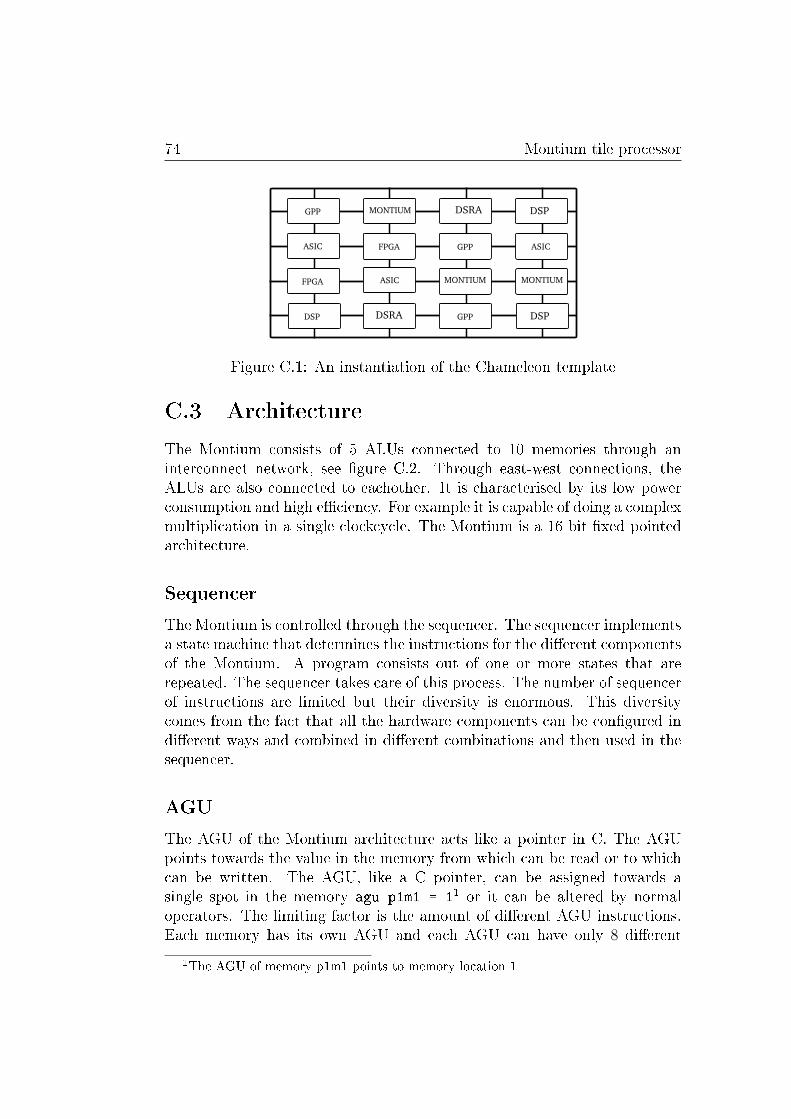
74 Montium tile processor
Figure C.1: An instantiation of the Chameleon template
C.3 Architecture
The Montium consists of 5 ALUs connected to 10 memories through aninterconnect network, see �gure C.2. Through east-west connections, theALUs are also connected to eachother. It is characterised by its low powerconsumption and high e�ciency. For example it is capable of doing a complexmultiplication in a single clockcycle. The Montium is a 16 bit �xed pointedarchitecture.
Sequencer
The Montium is controlled through the sequencer. The sequencer implementsa state machine that determines the instructions for the di�erent componentsof the Montium. A program consists out of one or more states that arerepeated. The sequencer takes care of this process. The number of sequencerof instructions are limited but their diversity is enormous. This diversitycomes from the fact that all the hardware components can be con�gured indi�erent ways and combined in di�erent combinations and then used in thesequencer.
AGU
The AGU of the Montium architecture acts like a pointer in C. The AGUpoints towards the value in the memory from which can be read or to whichcan be written. The AGU, like a C pointer, can be assigned towards asingle spot in the memory agu p1m1 = 11 or it can be altered by normaloperators. The limiting factor is the amount of di�erent AGU instructions.Each memory has its own AGU and each AGU can have only 8 di�erent
1The AGU of memory p1m1 points to memory location 1
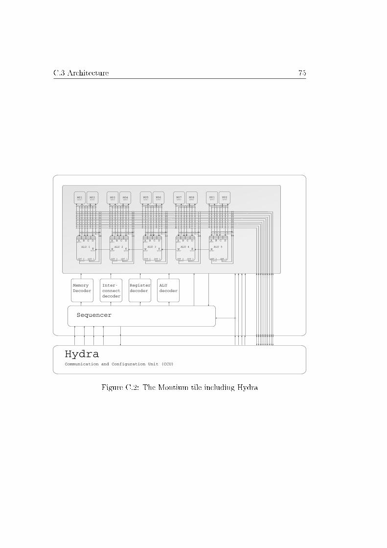
C.3 Architecture 75
Figure C.2: The Montium tile including Hydra
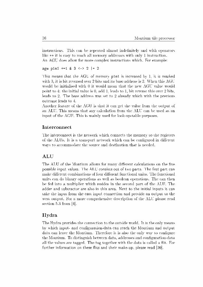
76 Montium tile processor
instructions. This can be repeated almost inde�nitely and with operatorslike ++ it is easy to reach all memory addresses with only 1 instruction.An AGU does allow for more complex instructions which. For example:
agu p1m1 +=1 & 3 <-> 2 |= 2
This means that the AGU of memory p1m1 is increased by 1, it is maskedwith 3, it is bit reversed over 2 bits and its base address is 2. When this AGUwould be initialised with 0 it would mean that the new AGU value wouldpoint to 4: the initial value is 0, add 1, leads to 1, bit reverse this over 2 bits,leads to 2. The base address was set to 2 already which with the previousoutcome leads to 4.Another feature of the AGU is that it can get the value from the output ofan ALU. This means that any calculation from the ALU can be used as aninput of the AGU. This is mainly used for look-up-table purposes.
Interconnect
The interconnect is the network which connects the memory to the registersof the ALUs. It is a transport network which can be con�gured in di�erentways to accommodate the source and destination that is needed.
ALU
The ALU of the Montium allows for many di�erent calculations on the �vepossible input values. The ALU consists out of two parts. The �rst part canmake di�erent combinations of four di�erent functional units. The functionalunits can do binary operations as well as boolean operations. The can thenbe fed into a multiplier which resides in the second part of the ALU. Theadder and subtractor are also in this area. Next to the initial inputs it cantake the input from the east input connection and provide an output to thewest output. For a more comprehensive description of the ALU please readsection 5.3 from [4].
Hydra
The Hydra provides the connection to the outside world. It is the only meansby which input- and con�guration-data can reach the Montium and outputdata can leave the Montium. Therefore it is also the only way to con�gurethe Montium. To distinguish between data, addresses and con�guration-dataall the values are tagged. The tag together with the data is called a �it. Forfurther information on these �its and their make-up, please read [20].
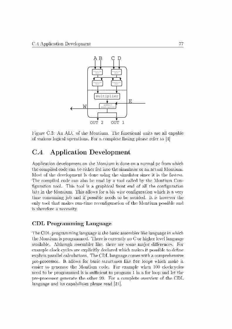
C.4 Application Development 77
Figure C.3: An ALU of the Montium. The functional units are all capableof various logical operations. For a complete listing please refer to [4]
C.4 Application Development
Application development on the Montium is done on a normal pc from whichthe compiled code can be either fed into the simulator or an actual Montium.Most of the development is done using the simulator since it is the fastest.The compiled code can also be read by a tool called by the Montium Con-�guration tool. This tool is a graphical front end of all the con�gurationbits in the Montium. This allows for a bit wise con�guration which is a verytime consuming job and if possible needs to be avoided. It is however theonly tool that makes run-time recon�guration of the Montium possible andis therefore a necessity.
CDL Programming Language
The CDL programming language is the basic assembler like language in whichthe Montium is programmed. There is currently no C or higher level languageavailable. Although assembler like, there are some major di�erences. Forexample clock cycles are explicitly declared which makes it possible to de�neexplicit parallel calculations. The CDL language comes with a comprehensivepre-processor. It allows for basic structures like for loops which make iteasier to generate the Montium code. For example when 100 clockcyclesneed to be programmed it is su�cient to program 1 in a for loop and let thepre-processor generate the other 99. For a complete overview of the CDLlanguage and its capabilities please read [21].
78 Montium tile processor
Simulator
There is a simulator available for the Montium. It is capable of simulatingthe Montium including or excluding the Hydra. For input and output ituses �les. These �les contain the con�guration data as well as the inputdata. All the current register values of the Montium can be read in a treewise fashion like in the way �les are read in a *nix prompt or old DOSprompt. This makes it di�cult to have certain values side by side since quitea few directory changes could be needed. The simulator can single cycle stepthrough the code generated but there is no way of going back or to break ata certain point. For more information on the simulator please read [22]As of writing this thesis a second simulator is in development that doeshave these features. Although it does not show as many parameters of theMontium it is far more friendlier to use if only functionality of the algorithmneeds to be tested. It has a graphical Java frontend and has the capabilityof stepping forward and backward and allows for a single breakpoint in thecode.
Matlab
Matlab is a tool to format the input and read the output �les. Matlabscripts either format only the input data in the correct order when thereis no simulation of the Hydra. In this mode the compiled code is directlyread by the simulator and Matlab's task is only to format the input data. Itcan also pack the con�guration data together with the input data when theHydra is part of the simulation. When the Hydra is simulated, Matlab's taskis to tag all the con�guration and input data according to the speci�cation[20].