pic16f193x/lf193x data sheet - 秋月電子通商akizukidenshi.com/download/pic16f193x.pdf · 2009...
TRANSCRIPT

2009 Microchip Technology Inc. Preliminary DS41364D
PIC16F193X/LF193XData Sheet
28/40/44-Pin Flash-Based, 8-Bit
CMOS Microcontrollers wtih
LCD Driver and nanoWatt XLP Technology

Note the following details of the code protection feature on Microchip devices:
• Microchip products meet the specification contained in their particular Microchip Data Sheet.
• Microchip believes that its family of products is one of the most secure families of its kind on the market today, when used in the intended manner and under normal conditions.
• There are dishonest and possibly illegal methods used to breach the code protection feature. All of these methods, to our knowledge, require using the Microchip products in a manner outside the operating specifications contained in Microchip’s Data Sheets. Most likely, the person doing so is engaged in theft of intellectual property.
• Microchip is willing to work with the customer who is concerned about the integrity of their code.
• Neither Microchip nor any other semiconductor manufacturer can guarantee the security of their code. Code protection does not mean that we are guaranteeing the product as “unbreakable.”
Code protection is constantly evolving. We at Microchip are committed to continuously improving the code protection features of ourproducts. Attempts to break Microchip’s code protection feature may be a violation of the Digital Millennium Copyright Act. If such actsallow unauthorized access to your software or other copyrighted work, you may have a right to sue for relief under that Act.
Information contained in this publication regarding deviceapplications and the like is provided only for your convenienceand may be superseded by updates. It is your responsibility toensure that your application meets with your specifications.MICROCHIP MAKES NO REPRESENTATIONS ORWARRANTIES OF ANY KIND WHETHER EXPRESS ORIMPLIED, WRITTEN OR ORAL, STATUTORY OROTHERWISE, RELATED TO THE INFORMATION,INCLUDING BUT NOT LIMITED TO ITS CONDITION,QUALITY, PERFORMANCE, MERCHANTABILITY ORFITNESS FOR PURPOSE. Microchip disclaims all liabilityarising from this information and its use. Use of Microchipdevices in life support and/or safety applications is entirely atthe buyer’s risk, and the buyer agrees to defend, indemnify andhold harmless Microchip from any and all damages, claims,suits, or expenses resulting from such use. No licenses areconveyed, implicitly or otherwise, under any Microchipintellectual property rights.
DS41364D-page 2 Prelimin
Trademarks
The Microchip name and logo, the Microchip logo, dsPIC, KEELOQ, KEELOQ logo, MPLAB, PIC, PICmicro, PICSTART, rfPIC and UNI/O are registered trademarks of Microchip Technology Incorporated in the U.S.A. and other countries.
FilterLab, Hampshire, HI-TECH C, Linear Active Thermistor, MXDEV, MXLAB, SEEVAL and The Embedded Control Solutions Company are registered trademarks of Microchip Technology Incorporated in the U.S.A.
Analog-for-the-Digital Age, Application Maestro, CodeGuard, dsPICDEM, dsPICDEM.net, dsPICworks, dsSPEAK, ECAN, ECONOMONITOR, FanSense, HI-TIDE, In-Circuit Serial Programming, ICSP, Mindi, MiWi, MPASM, MPLAB Certified logo, MPLIB, MPLINK, mTouch, Octopus, Omniscient Code Generation, PICC, PICC-18, PICDEM, PICDEM.net, PICkit, PICtail, PIC32 logo, REAL ICE, rfLAB, Select Mode, Total Endurance, TSHARC, UniWinDriver, WiperLock and ZENA are trademarks of Microchip Technology Incorporated in the U.S.A. and other countries.
SQTP is a service mark of Microchip Technology Incorporated in the U.S.A.
All other trademarks mentioned herein are property of their respective companies.
© 2009, Microchip Technology Incorporated, Printed in the U.S.A., All Rights Reserved.
Printed on recycled paper.
ary 2009 Microchip Technology Inc.
Microchip received ISO/TS-16949:2002 certification for its worldwide headquarters, design and wafer fabrication facilities in Chandler and Tempe, Arizona; Gresham, Oregon and design centers in California and India. The Company’s quality system processes and procedures are for its PIC® MCUs and dsPIC® DSCs, KEELOQ® code hopping devices, Serial EEPROMs, microperipherals, nonvolatile memory and analog products. In addition, Microchip’s quality system for the design and manufacture of development systems is ISO 9001:2000 certified.

PIC16F193X/LF193X28/40/44-Pin Flash-Based, 8-Bit CMOS Microcontrollers with
LCD Driver with nanoWatt XLP Technology
Devices Included In This Data Sheet:
PIC16F193X Devices:
PIC16LF193X Devices:
High-Performance RISC CPU:
• Only 49 Instructions to Learn:- All single-cycle instructions except branches
• Operating Speed:- DC – 32 MHz oscillator/clock input- DC – 125 ns instruction cycle
• Up to 16K x 14 Words of Flash Program Memory• Up to 1024 Bytes of Data Memory (RAM)• Interrupt Capability with automatic context saving• 16-Level Deep Hardware Stack• Direct, Indirect and Relative Addressing modes• Processor Read Access to Program Memory• Pinout Compatible to other 28/40-pin PIC16CXXX
and PIC16FXXX Microcontrollers
Special Microcontroller Features:
• Precision Internal Oscillator:- Factory calibrated to ±1%, typical- Software selectable frequency range from
32 MHz to 31 kHz• Power-Saving Sleep mode• Power-on Reset (POR)• Power-up Timer (PWRT) and Oscillator Start-up
Timer (OST)• Brown-out Reset (BOR)
- Selectable between two trip points- Disable in Sleep option
• Multiplexed Master Clear with Pull-up/Input Pin• Programmable Code Protection• High Endurance Flash/EEPROM cell:
- 100,000 write Flash endurance- 1,000,000 write EEPROM endurance- Flash/Data EEPROM retention: > 40 years
• Wide Operating Voltage Range:- 1.8V-5.5V (PIC16F193X)- 1.8V-3.6V (PIC16LF193X)
PIC16LF193X Low-Power Features:
• Standby Current:- 60 nA @ 1.8V, typical
• Operating Current:- 7.0 A @ 32 kHz, 1.8V, typical (PIC16LF193X)- 150 A @ 1 MHz, 1.8V, typical (PIC16LF193X)
• Timer1 Oscillator Current:- 600 nA @ 32 kHz, 1.8V, typical
• Low-Power Watchdog Timer Current:- 500 nA @ 1.8V, typical (PIC16LF193X)
Peripheral Features:• Up to 35 I/O Pins and 1 Input-only pin:
- High-current source/sink for direct LED drive- Individually programmable Interrupt-on-pin
change pins- Individually programmable weak pull-ups
• Integrated LCD Controller:- Up to 96 segments- Variable clock input- Contrast control- Internal voltage reference selections
• Capacitive Sensing Module (mTouchTM)- Up to 16 selectable channels
• A/D Converter:- 10-bit resolution and up to 14 channels- Selectable 1.024/2.048/4.096V voltage
reference• Timer0: 8-Bit Timer/Counter with 8-Bit
Programmable Prescaler• Enhanced Timer1
- Dedicated low-power 32 kHz oscillator driver- 16-bit timer/counter with prescaler- External Gate Input mode with toggle and
single shot modes - Interrupt-on-gate completion
• Timer2, 4, 6: 8-Bit Timer/Counter with 8-Bit Period Register, Prescaler and Postscaler
• Two Capture, Compare, PWM Modules (CCP)- 16-bit Capture, max. resolution 125 ns- 16-bit Compare, max. resolution 125 ns- 10-bit PWM, max. frequency 31.25 kHz
• Three Enhanced Capture, Compare, PWM modules (ECCP)- 3 PWM time-base options- Auto-shutdown and auto-restart- PWM steering- Programmable Dead-band Delay
• PIC16F1933 • PIC16F1934
• PIC16F1936 • PIC16F1937
• PIC16F1938 • PIC16F1939
• PIC16LF1933 • PIC16LF1934
• PIC16LF1936 • PIC16LF1937
• PIC16LF1938 • PIC16LF1939
2009 Microchip Technology Inc. Preliminary DS41364D-page 3
PIC16F193X/LF193X
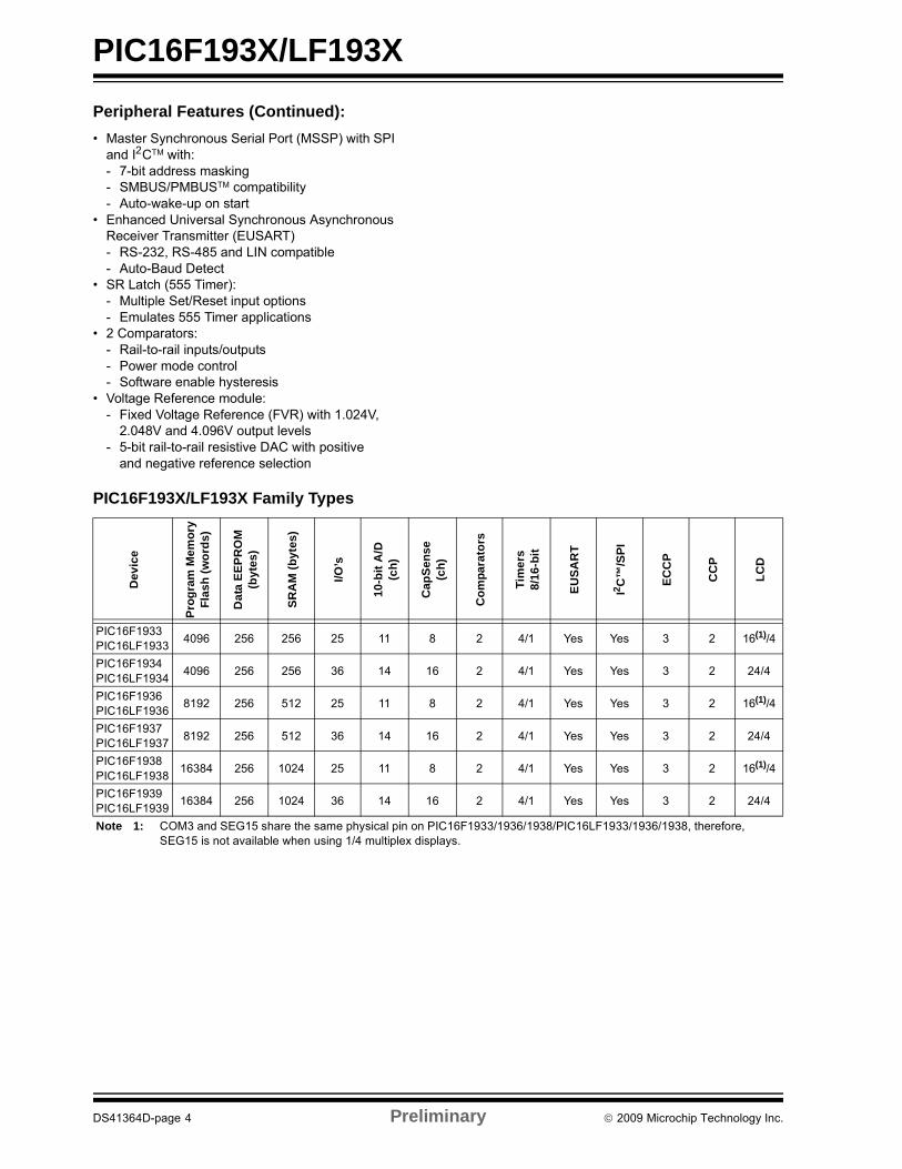
Peripheral Features (Continued):
• Master Synchronous Serial Port (MSSP) with SPI and I2 CTM with:- 7-bit address masking- SMBUS/PMBUSTM compatibility- Auto-wake-up on start
• Enhanced Universal Synchronous Asynchronous Receiver Transmitter (EUSART)- RS-232, RS-485 and LIN compatible- Auto-Baud Detect
• SR Latch (555 Timer):- Multiple Set/Reset input options- Emulates 555 Timer applications
• 2 Comparators:- Rail-to-rail inputs/outputs - Power mode control- Software enable hysteresis
• Voltage Reference module:- Fixed Voltage Reference (FVR) with 1.024V,
2.048V and 4.096V output levels- 5-bit rail-to-rail resistive DAC with positive
and negative reference selection
PIC16F193X/LF193X Family Types
De
vic
e
Pro
gra
m M
em
ory
Fla
sh
(w
ord
s)
Da
ta E
EP
RO
M(b
yte
s)
SR
AM
(b
yte
s)
I/O
’s
10
-bit
A/D
(ch
)
Ca
pS
en
se
(ch
)
Co
mp
ara
tors
Tim
ers
8/1
6-b
it
EU
SA
RT
I2C
™/S
PI
EC
CP
CC
P
LC
D
PIC16F1933PIC16LF1933
4096 256 256 25 11 8 2 4/1 Yes Yes 3 2 16(1)/4
PIC16F1934PIC16LF1934
4096 256 256 36 14 16 2 4/1 Yes Yes 3 2 24/4
PIC16F1936PIC16LF1936
8192 256 512 25 11 8 2 4/1 Yes Yes 3 2 16(1)/4
PIC16F1937PIC16LF1937
8192 256 512 36 14 16 2 4/1 Yes Yes 3 2 24/4
PIC16F1938PIC16LF1938
16384 256 1024 25 11 8 2 4/1 Yes Yes 3 2 16(1)/4
PIC16F1939PIC16LF1939
16384 256 1024 36 14 16 2 4/1 Yes Yes 3 2 24/4
Note 1: COM3 and SEG15 share the same physical pin on PIC16F1933/1936/1938/PIC16LF1933/1936/1938, therefore, SEG15 is not available when using 1/4 multiplex displays.
DS41364D-page 4 Preliminary 2009 Microchip Technology Inc.

PIC16F193X/LF193X
Pin Diagram – 28-Pin SPDIP/SOIC/SSOP (PIC16F1933/1936/1938, PIC16LF1933/1936/1938)
28-pin SPDIP, SOIC, SSOP
PIC
16F
193
3/1
936
/193
8
PIC
16L
F19
33/1
936
/193
8
1
2
3
4
5
6
7
8
9
10
VPP/MCLR/RE3
SEG12/VCAP(2)/SS(1)/SRNQ(1)/C2OUT(1)/C12IN0-/AN0/RA0
SEG7/C12IN1-/AN1/RA1
COM2/DACOUT/VREF-/C2IN+/AN2/RA2
SEG15/COM3/VREF+/C1IN+/AN3/RA3
SEG4/CCP5/SRQ/T0CKI/CPS6/C1OUT/RA4
SEG5/VCAP(2)/SS(1)/SRNQ(1)/CPS7/C2OUT(1)/AN4/RA5
RB6/ICSPCLK/ICDCLK/SEG14
RB5/AN13/CPS5/P2B(1)/CCP3(1)/P3A(1)/T1G(1)/COM1
RB4/AN11/CPS4/P1D/COM0
RB3/AN9/C12IN2-/CPS3/CCP2(1)/P2A(1)/VLCD3
RB2/AN8/CPS2/P1B/VLCD2
RB1/AN10/C12IN3-/CPS1/P1C/VLCD1RB0/AN12/CPS0/CCP4/SRI/INT/SEG0
VDD
VSS
11
12
13
14 15
16
17
18
19
20
28
27
26
25
24
23
2221VSS
SEG2/CLKIN/OSC1/RA7
SEG1/VCAP(2)/CLKOUT/OSC2/RA6
P2B(1)/T1CKI/T1OSO/RC0
P2A(1)/CCP2(1)/T1OSI/RC1
SEG3/P1A/CCP1/RC2
SEG6/SCL/SCK/RC3
RC5/SDO/SEG10
RC4/SDI/SDA/T1G(1)/SEG11
RC7/RX/DT/P3B/SEG8
RC6/TX/CK/CCP3(1)/P3A(1)/SEG9
RB7/ICSPDAT/ICDDAT/SEG13
Note 1: Pin function is selectable via the APFCON register.
2: PIC16F193X devices only.
2009 Microchip Technology Inc. Preliminary DS41364D-page 5
PIC16F193X/LF193X
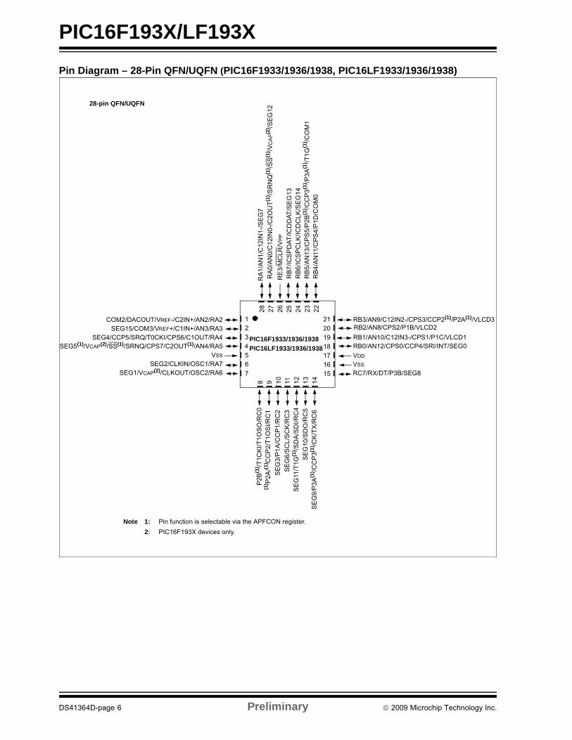
Pin Diagram – 28-Pin QFN/UQFN (PIC16F1933/1936/1938, PIC16LF1933/1936/1938)
2
3
6
1
18
19
20
21
15716
17
P2B
(1) /T
1CK
I/T1O
SO
/RC
0
54
RB
7/IC
SP
DA
T/IC
DD
AT
/SE
G13
RB
6/I
CS
PC
LK/I
CD
CLK
/SE
G1
4R
B5
/AN
13/C
PS
5/P
2B(1
) /CC
P3
(1) /P
3A(1
) /T1
G(1
) /CO
M1
RB
4/A
N11
/CP
S4
/P1D
/CO
M0
RB3/AN9/C12IN2-/CPS3/CCP2(1)/P2A(1)/VLCD3RB2/AN8/CPS2/P1B/VLCD2
RB1/AN10/C12IN3-/CPS1/P1C/VLCD1RB0/AN12/CPS0/CCP4/SRI/INT/SEG0
VDD
VSS
RC7/RX/DT/P3B/SEG8
SE
G9
/P3A
(1) /C
CP
3(1) /C
K/T
X/R
C6
SE
G10
/SD
O/R
C5
SE
G11
/T1G
(1) /S
DA
/SD
I/R
C4
RE
3/M
CL
R/V
PP
RA
0/A
N0/
C1
2IN
0-/
C2O
UT
(1) /S
RN
Q(1
) /SS
(1) /V
CA
P(2
) /SE
G12
RA
1/A
N1
/C12
IN1-
/SE
G7
COM2/DACOUT/VREF-/C2IN+/AN2/RA2SEG15/COM3/VREF+/C1IN+/AN3/RA3
SEG4/CCP5/SRQ/T0CKI/CPS6/C1OUT/RA4SEG5(1)/VCAP(2)/SS(1)/SRNQ/CPS7/C2OUT(1)/AN4/RA5
VSS
SEG2/CLKIN/OSC1/RA7SEG1/VCAP(2)/CLKOUT/OSC2/RA6
(1) P
2A/(1
) CC
P2/
T1
OS
I/R
C1
SE
G3/
P1
A/C
CP
1/R
C2
SE
G6
/SC
L/S
CK
/RC
3
9 10
13
8 14
12
11
27
26
23
28
22
24
25
PIC16F1933/1936/1938
PIC16LF1933/1936/1938
28-pin QFN/UQFN
Note 1: Pin function is selectable via the APFCON register.
2: PIC16F193X devices only.
DS41364D-page 6 Preliminary 2009 Microchip Technology Inc.

PIC16F193X/LF193X
)
)
/T)
/
K/K
T/T
PP
TABLE 1: 28-PIN SUMMARY (PIC16F1933/1936/1938, PIC16LF1933/1936/1938)
I/O
28-P
in S
IP
28-P
in Q
FN
/UQ
FN
AN
SE
L
A/D
Cap
Sen
se
Co
mp
arat
or
SR
Lat
ch
Tim
ers
CC
P
EU
SA
RT
MS
SP
LC
D
Inte
rru
pt
Pu
ll-u
p
Bas
ic
RA0 2 27 Y AN0 — C12IN0-/C2OUT(1) SRNQ(1) — — —
SS(1) SEG12 — — VCAP(2
RA1 3 28 Y AN1 — C12IN1- — — — — — SEG7 — — —
RA2 4 1 Y AN2/VREF-
— C2IN+/DACOUT
— — — — — COM2 — — —
RA3 5 2 Y AN3/VREF+
— C1IN+ — — — — — SEG15/COM3
— — —
RA4 6 3 Y — CPS6 C1OUT SRQ T0CKI CCP5 — — SEG4 — — —
RA5 7 4 Y AN4 CPS7 C2OUT(1) SRNQ(1) — — — SS(1) SEG5 — — VCAP(2
RA6 10 7 — — — — — — — — — SEG1 — — OSC2CLKOUVCAP(2
RA7 9 6 — — — — — — — — — SEG2 — — OSC1CLKIN
RB0 21 18 Y AN12 CPS0 — SRI — CCP4 — — SEG0 INT/IOC
Y —
RB1 22 19 Y AN10 CPS1 C12IN3- — — P1C — — VLCD1 IOC Y —
RB2 23 20 Y AN8 CPS2 — — — P1B — — VLCD2 IOC Y —
RB3 24 21 Y AN9 CPS3 C12IN2- — — CCP2(1)/P2A(1)
— — VLCD3 IOC Y —
RB4 25 22 Y AN11 CPS4 — — — P1D — — COM0 IOC Y —
RB5 26 23 Y AN13 CPS5 — — T1G(1) P2B(1)
CCP3(1)/P3A(1)
— — COM1 IOC Y —
RB6 27 24 — — — — — — — — — SEG14 IOC Y ICSPCLICDCL
RB7 28 25 — — — — — — — — — SEG13 IOC Y ICSPDAICDDA
RC0 11 8 — — — — — T1OSO/T1CKI
P2B(1) — — — — — —
RC1 12 9 — — — — — T1OSI CCP2(1)/P2A(1)
— — — — — —
RC2 13 10 — — — — — — CCP1/P1A
— — SEG3 — — —
RC3 14 11 — — — — — — — — SCK/SCL SEG6 — — —
RC4 15 12 — — — — — T1G(1) — — SDI/SDA SEG11 — — —
RC5 16 13 — — — — — — — — SDO SEG10 — — —
RC6 17 14 — — — — — — CCP3(1)
P3A(1)TX/CK — SEG9 — — —
RC7 18 15 — — — — — — P3B RX/DT — SEG8 — — —
RE3 1 26 — — — — — — — — — — — Y MCLR/V
VDD 20 17 — — — — — — — — — — — — VDD
Vss 8,19
5,16
— — — — — — — — — — — — VSS
Note 1: Pin functions can be moved using the APFCON register.2: PIC16F193X devices only.
2009 Microchip Technology Inc. Preliminary DS41364D-page 7
PIC16F193X/LF193X
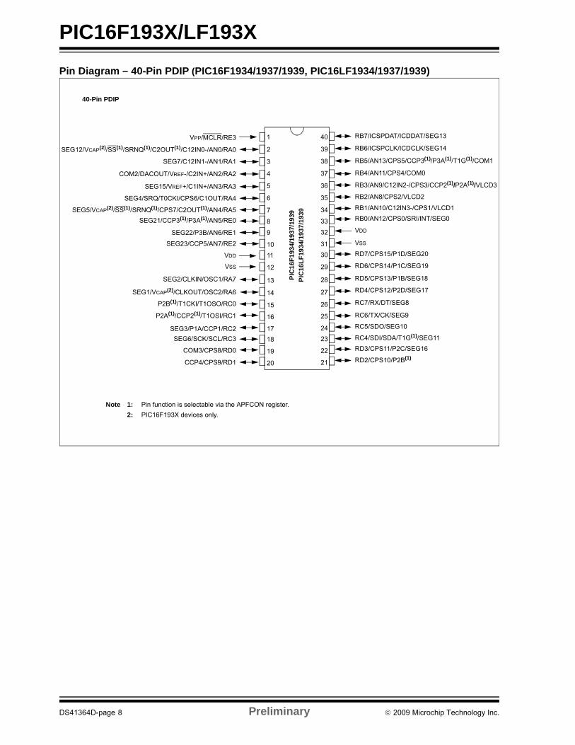
Pin Diagram – 40-Pin PDIP (PIC16F1934/1937/1939, PIC16LF1934/1937/1939)
40-Pin PDIP
PIC
16F
193
4/1
937
/193
9
PIC
16L
F19
34/1
937/
193
9
2
3
4
5
6
7
8
9
10
VPP/MCLR/RE3
SEG12/VCAP(2)/SS(1)/SRNQ(1)/C2OUT(1)/C12IN0-/AN0/RA0
SEG7/C12IN1-/AN1/RA1
COM2/DACOUT/VREF-/C2IN+/AN2/RA2
SEG15/VREF+/C1IN+/AN3/RA3
SEG4/SRQ/T0CKI/CPS6/C1OUT/RA4
SEG5/VCAP(2)/SS(1)/SRNQ(1)/CPS7/C2OUT(1)/AN4/RA5
SEG21/CCP3(1)/P3A(1)/AN5/RE0
SEG22/P3B/AN6/RE1
SEG23/CCP5/AN7/RE2
RB6/ICSPCLK/ICDCLK/SEG14
RB5/AN13/CPS5/CCP3(1)/P3A(1)/T1G(1)/COM1
RB4/AN11/CPS4/COM0
RB3/AN9/C12IN2-/CPS3/CCP2(1)/P2A(1)/VLCD3
RB2/AN8/CPS2/VLCD2
RB1/AN10/C12IN3-/CPS1/VLCD1
RB0/AN12/CPS0/SRI/INT/SEG0
VDD
VSS
RD2/CPS10/P2B(1)
11
12
13
14
15
16
17
18
19
20
40
39
38
37
36
35
34
33
32
31
30
29
28
27
26
25
24
23
22
21
VDD
VSS
SEG2/CLKIN/OSC1/RA7
SEG1/VCAP(2)/CLKOUT/OSC2/RA6
P2B(1)/T1CKI/T1OSO/RC0
P2A(1)/CCP2(1)/T1OSI/RC1
SEG3/P1A/CCP1/RC2
SEG6/SCK/SCL/RC3
COM3/CPS8/RD0
CCP4/CPS9/RD1
RC5/SDO/SEG10
RC4/SDI/SDA/T1G(1)/SEG11
RD3/CPS11/P2C/SEG16
RD4/CPS12/P2D/SEG17
RC7/RX/DT/SEG8
RC6/TX/CK/SEG9
RD7/CPS15/P1D/SEG20
RD6/CPS14/P1C/SEG19
RD5/CPS13/P1B/SEG18
RB7/ICSPDAT/ICDDAT/SEG131
Note 1: Pin function is selectable via the APFCON register.
2: PIC16F193X devices only.
DS41364D-page 8 Preliminary 2009 Microchip Technology Inc.
PIC16F193X/LF193X
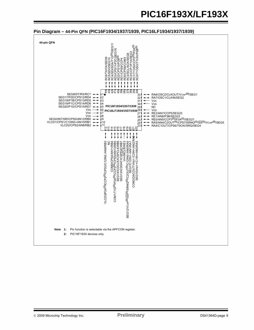
Pin Diagram – 44-Pin QFN (PIC16F1934/1937/1939, PIC16LF1934/1937/1939)
1011
23456
1
18
19
20
21 22
12
13
14
15
38
87
44 43 42 41 40 391
61
7
2930313233
232425262728
36 3435
9
37S
EG
7/C
12IN
1-/A
N1/
RA
1S
EG
12/V
CA
P(2
) /SS
(1) /S
RN
Q(1
) /C2
OU
T(1
) /C12
IN0-
/AN
0/R
A0
VP
P/M
CLR
/RE
3
VLC
D3
/P2A
(1) /C
CP
2(1) /C
PS
3/C
12IN
2-/A
N9/
RB
3
SE
G1
3/IC
DD
AT
/ICS
PD
AT
/RB
7S
EG
14/I
CD
CL
K/I
CS
PC
LK/R
B6
CO
M1/
T1G
(1) /P
3A
(1) /C
CP
3(1) /C
PS
5/A
N1
3/R
B5
CO
M0/
CP
S4/
AN
11/R
B4
NC
RC
6/T
X/C
K/S
EG
9R
C5
/SD
O/S
EG
10
RC
4/S
DI/S
DA
/T1G
(1) /S
EG
11R
D3
/CP
S11
/P2C
/SE
G16
RD
2/C
PS
10/P
2B
(1)
RD
1/C
PS
9/C
CP
4R
D0
/CP
S8/
CO
M3
RC
3/S
CL/
SC
K/S
EG
6R
C2
/CC
P1/
P1
A/S
EG
3R
C1
/T1
OS
I/C
CP
2(1
) /P2A
(1)
RC
0/T
1O
SO
/T1C
KI/
P2
B(1
)
RA6/OSC2/CLKOUT/VCAP(2)/SEG1RA7/OSC1/CLKIN/SEG2VSSVSSNCVDDRE2/AN7/CCP5/SEG23RE1/AN6/P3B/SEG22RE0/AN5/CCP3(1)/P3A(1)/SEG21RA5/AN4/C2OUT(1)/CPS7/SRNQ(1)/SS(1)/VCAP(2)/SEG5RA4/C1OUT/CPS6/T0CKI/SRQ/SEG4
SEG8/DT/RX/RC7SEG17/P2D/CPS12/RD4SEG18/P1B/CPS13/RD5SEG19/P1C/CPS14/RD6SEG20/P1D/CPS15/RD7
VSSVDDVDD
SEG0/INT/SRI/CPS0/AN12/RB0VLCD1/CPS1/C12IN3-/AN10/RB1
VLCD2/CPS2/AN8/RB2
44-pin QFN
PIC16F1934/1937/1939
PIC16LF1934/1937/1939
SE
G15
VR
EF+
/C1I
N+
/AN
3/R
A3
CO
M2
/DA
CO
UT
/VR
EF-/
C2
IN+
/AN
2/R
A2
Note 1: Pin function is selectable via the APFCON register.
2: PIC16F193X devices only.
2009 Microchip Technology Inc. Preliminary DS41364D-page 9

PIC16F193X/LF193X
Pin Diagram – 44-Pin TQFP (PIC16F1934/1937/1939, PIC16LF1934/1937/1939)
44-pin TQFP
1011
23
6
1
18 19 20 21 2212 13 14 15
38
87
44
43 42 41 40 39
16 17
2930313233
232425262728
36 3435
9
37
SE
G15
/VR
EF+
/C1I
N+
/AN
3/R
A3
CO
M2/
DA
CO
UT
/VR
EF-/
C2I
N+
/AN
2/R
A2
SE
G7/
C12
IN1-
/AN
1/R
A1
SE
G12
/VC
AP
(2) /S
S(1
) /SR
NQ
(1) /C
2O
UT
(1) /C
12IN
0-/A
N0/
RA
0V
PP/M
CLR
/RE
3
NC
SE
G13
/IC
DD
AT
/IC
SP
DA
T/R
B7
SE
G14
/IC
DC
LK
/IC
SP
CLK
/RB
6C
OM
1/T
1G(1
) /P3
A(1
) /CC
P3(1
) /CP
S5/
AN
13/
RB
5C
OM
0/C
PS
4/A
N11
/RB
4N
C
NC
NCRC0/T1OSO/T1CKI/P2B(1)
VSSVDD
SEG0/INT/SRI/CPS0/AN12/RB0VLCD1/CPS1/C12IN3-/AN10/RB1
VLCD2/CPS2/AN8/RB2VLCD3/P2A(1)/CCP2(1)/CPS3/C12IN2-/AN9/RB3
54
PIC16F1934/1937/1939PIC16LF1934/1937/1939
RA6/OSC2/CLKOUT/VCAP(2)/SEG1RA7/OSC1/CLKIN/SEG2VSSVDD
RE2/AN7/CCP5/SEG23RE1/AN6/P3B/SEG22RE0/AN5/CCP3(1)/P3A(1)/SEG21RA5/AN4/C2OUT(1)/CPS7/SRNQ(1)/SS(1)/VCAP(2)/SEG5RA4/C1OUT/CPS6/T0CKI/SRQ/SEG4
SEG8/DT/RX/RC7SEG17/P2D/CPS12/RD4SEG18/P1B/CPS13/RD5SEG19/P1C/CPS14/RD6SEG20/P1D/CPS15/RD7
RC
6/T
X/C
K/S
EG
9R
C5
/SD
O/S
EG
10
RC
4/S
DI/S
DA
/T1G
(1) /S
EG
11R
D3/
CP
S11
/P2C
/SE
G1
6R
D2/
CP
S1
0/P
2B(1
)
RD
1/C
PS
9/C
CP
4R
D0
/CP
S8/
CO
M3
RC
3/S
CL
/SC
K/S
EG
6R
C2/
CC
P1
/P1A
/SE
G3
RC
1/T
1OS
I/C
CP
2(1) /P
2A(1
)
Note 1: Pin function is selectable via the APFCON register.
2: PIC16F193X devices only.
DS41364D-page 10 Preliminary 2009 Microchip Technology Inc.

PIC16F193X/LF193X
Bas
ic
P
P
2/UTP
1/IN
LK/LK
AT/AT
/VPP
D
S
TABLE 2: 40/44-PIN SUMMARY(PIC16F1934/1937/1939, PIC16LF1934/1937/1939)
I/O
40-P
in P
DIP
44-
Pin
TQ
FP
44-
Pin
QF
N
AN
SE
L
A/D
Cap
Sen
se
Co
mp
arat
or
SR
Lat
ch
Tim
ers
CC
P
EU
SA
RT
MS
SP
LC
D
Inte
rru
pt
Pu
ll-u
p
RA0 2 19 19 Y AN0 — C12IN0-/C2OUT(1) SRNQ(1) — — —
SS(1) SEG12 — — VCA
RA1 3 20 20 Y AN1 — C12IN1- — — — — — SEG7 — — —
RA2 4 21 21 Y AN2/VREF-
— C2IN+/DACOUT
— — — — — COM2 — — —
RA3 5 22 22 Y AN3/VREF+
— C1IN+ — — — — — SEG15 — — —
RA4 6 23 23 Y — CPS6 C1OUT SRQ T0CKI — — SEG4 — — —
RA5 7 24 24 Y AN4 CPS7 C2OUT(1) SRNQ(1) — — — SS(1) SEG5 — — VCA
RA6 14 31 33 — — — — — — — — — SEG1 — — OSCCLKO
VCA
RA7 13 30 32 — — — — — — — — — SEG2 — — OSCCLK
RB0 33 8 9 Y AN12 CPS0 — SRI — — — — SEG0 INT/IOC
Y —
RB1 34 9 10 Y AN10 CPS1 C12IN3- — — — — — VLCD1 IOC Y —
RB2 35 10 11 Y AN8 CPS2 — — — — — — VLCD2 IOC Y —
RB3 36 11 12 Y AN9 CPS3 C12IN2- — — CCP2(1)/P2A(1)
— — VLCD3 IOC Y —
RB4 37 14 14 Y AN11 CPS4 — — — — — — COM0 IOC Y —
RB5 38 15 15 Y AN13 CPS5 — — T1G(1) CCP3(1)/P3A(1)
— — COM1 IOC Y —
RB6 39 16 16 — — — — — — — — — SEG14 IOC Y ICSPCICDC
RB7 40 17 17 — — — — — — — — — SEG13 IOC Y ICSPDICDD
RC0 15 32 34 — — — — — T1OSO/T1CKI
P2B(1) — — — — — —
RC1 16 35 35 — — — — — T1OSI CCP2(1)/P2A(1)
— — — — — —
RC2 17 36 36 — — — — — — CCP1/P1A
— — SEG3 — — —
RC3 18 37 37 — — — — — — — — SCK/SCL SEG6 — — —
RC4 23 42 42 — — — — — T1G(1) — — SDI/SDA SEG11 — — —
RC5 24 43 43 — — — — — — — — SDO SEG10 — — —
RC6 25 44 44 — — — — — — — TX/CK — SEG9 — — —
RC7 26 1 1 — — — — — — — RX/DT — SEG8 — — —
RD0 19 38 38 Y — CPS8 — — — — — — COM3 — — —
RD1 20 39 39 Y — CPS9 — — — CCP4 — — — — — —
RD2 21 40 40 Y — CPS10 — — — P2B(1) — — — — — —
RD3 22 41 41 Y — CPS11 — — — P2C — — SEG16 — — —
RD4 27 2 2 Y — CPS12 — — — P2D — — SEG17 — — —
RD5 28 3 3 Y — CPS13 — — — P1B — — SEG18 — — —
RD6 29 4 4 Y — CPS14 — — — P1C — — SEG19 — — —
RD7 30 5 5 Y — CPS15 — — — P1D — — SEG20 — — —
RE0 8 25 25 Y AN5 — — — — CCP3(1)
P3A(1)— — SEG21 — — —
RE1 9 26 26 Y AN6 — — — — P3B — — SEG22 — — —
RE2 10 27 27 Y AN7 — — — — CCP5 — — SEG23 — — —
RE3 1 18 18 — — — — — — — — — — — Y MCLR
VDD 11,32
7,28
7,8,28
— — — — — — — — — — — — VD
Vss 12,31
6,29
6,30,31
— — — — — — — — — — — — VS
Note 1: Pin functions can be moved using the APFCON register.
2009 Microchip Technology Inc. Preliminary DS41364D-page 11
PIC16F193X/LF193X
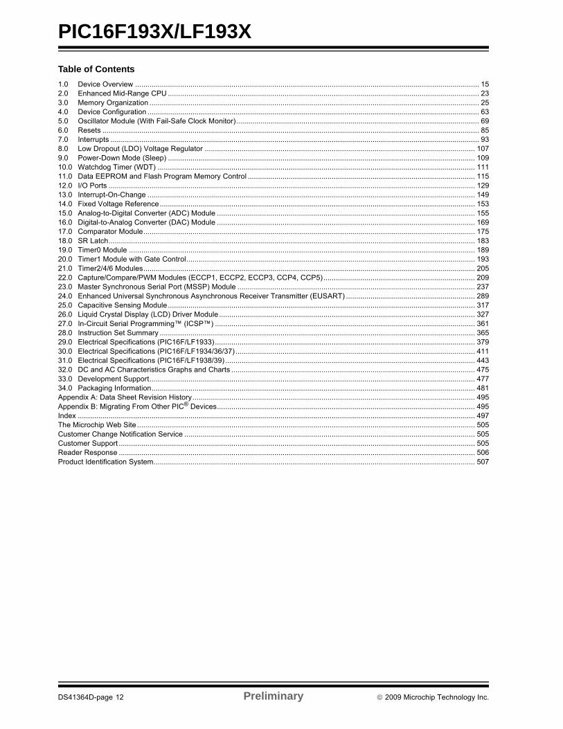
Table of Contents
1.0 Device Overview ........................................................................................................................................................................ 152.0 Enhanced Mid-Range CPU ........................................................................................................................................................ 233.0 Memory Organization ................................................................................................................................................................. 254.0 Device Configuration .................................................................................................................................................................. 635.0 Oscillator Module (With Fail-Safe Clock Monitor)....................................................................................................................... 696.0 Resets ........................................................................................................................................................................................ 857.0 Interrupts .................................................................................................................................................................................... 938.0 Low Dropout (LDO) Voltage Regulator .................................................................................................................................... 1079.0 Power-Down Mode (Sleep) ...................................................................................................................................................... 10910.0 Watchdog Timer (WDT) ........................................................................................................................................................... 11111.0 Data EEPROM and Flash Program Memory Control ............................................................................................................... 11512.0 I/O Ports ................................................................................................................................................................................... 12913.0 Interrupt-On-Change ................................................................................................................................................................ 14914.0 Fixed Voltage Reference.......................................................................................................................................................... 15315.0 Analog-to-Digital Converter (ADC) Module .............................................................................................................................. 15516.0 Digital-to-Analog Converter (DAC) Module .............................................................................................................................. 16917.0 Comparator Module.................................................................................................................................................................. 17518.0 SR Latch................................................................................................................................................................................... 18319.0 Timer0 Module ......................................................................................................................................................................... 18920.0 Timer1 Module with Gate Control............................................................................................................................................. 19321.0 Timer2/4/6 Modules.................................................................................................................................................................. 20522.0 Capture/Compare/PWM Modules (ECCP1, ECCP2, ECCP3, CCP4, CCP5) .......................................................................... 20923.0 Master Synchronous Serial Port (MSSP) Module .................................................................................................................... 23724.0 Enhanced Universal Synchronous Asynchronous Receiver Transmitter (EUSART) ............................................................... 28925.0 Capacitive Sensing Module...................................................................................................................................................... 31726.0 Liquid Crystal Display (LCD) Driver Module............................................................................................................................. 32727.0 In-Circuit Serial Programming™ (ICSP™) ............................................................................................................................... 36128.0 Instruction Set Summary .......................................................................................................................................................... 36529.0 Electrical Specifications (PIC16F/LF1933)............................................................................................................................... 37930.0 Electrical Specifications (PIC16F/LF1934/36/37) ..................................................................................................................... 41131.0 Electrical Specifications (PIC16F/LF1938/39) .......................................................................................................................... 44332.0 DC and AC Characteristics Graphs and Charts ....................................................................................................................... 47533.0 Development Support............................................................................................................................................................... 47734.0 Packaging Information.............................................................................................................................................................. 481Appendix A: Data Sheet Revision History.......................................................................................................................................... 495Appendix B: Migrating From Other PIC® Devices.............................................................................................................................. 495Index .................................................................................................................................................................................................. 497The Microchip Web Site ..................................................................................................................................................................... 505Customer Change Notification Service .............................................................................................................................................. 505Customer Support .............................................................................................................................................................................. 505Reader Response .............................................................................................................................................................................. 506Product Identification System............................................................................................................................................................. 507
DS41364D-page 12 Preliminary 2009 Microchip Technology Inc.
PIC16F193X/LF193X
TO OUR VALUED CUSTOMERS
It is our intention to provide our valued customers with the best documentation possible to ensure successful use of your Microchipproducts. To this end, we will continue to improve our publications to better suit your needs. Our publications will be refined andenhanced as new volumes and updates are introduced.
If you have any questions or comments regarding this publication, please contact the Marketing Communications Department viaE-mail at [email protected] or fax the Reader Response Form in the back of this data sheet to (480) 792-4150.We welcome your feedback.
Most Current Data Sheet
To obtain the most up-to-date version of this data sheet, please register at our Worldwide Web site at:
http://www.microchip.com
You can determine the version of a data sheet by examining its literature number found on the bottom outside corner of any page.The last character of the literature number is the version number, (e.g., DS30000A is version A of document DS30000).
Errata
An errata sheet, describing minor operational differences from the data sheet and recommended workarounds, may exist for currentdevices. As device/documentation issues become known to us, we will publish an errata sheet. The errata will specify the revisionof silicon and revision of document to which it applies.
To determine if an errata sheet exists for a particular device, please check with one of the following:
• Microchip’s Worldwide Web site; http://www.microchip.com• Your local Microchip sales office (see last page)• The Microchip Corporate Literature Center; U.S. FAX: (480) 792-7277
When contacting a sales office or the literature center, please specify which device, revision of silicon and data sheet (includeliterature number) you are using.
Customer Notification System
Register on our web site at www.microchip.com/cn to receive the most current information on all of our products.
2009 Microchip Technology Inc. Preliminary DS41364D-page 13

PIC16F193X/LF193X
NOTES:
DS41364D-page 14 Preliminary 2009 Microchip Technology Inc.
PIC16F193X/LF193X
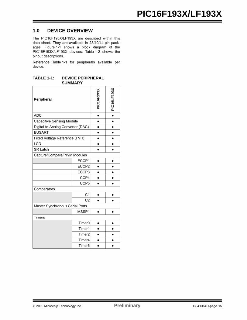
1.0 DEVICE OVERVIEW
The PIC16F193X/LF193X are described within thisdata sheet. They are available in 28/40/44-pin pack-ages. Figure 1-1 shows a block diagram of thePIC16F193X/LF193X devices. Table 1-2 shows thepinout descriptions.
Reference Table 1-1 for peripherals available perdevice.
TABLE 1-1: DEVICE PERIPHERAL SUMMARY
Peripheral P
IC16
F19
3X
PIC
16L
F1
93X
ADC ● ●
Capacitive Sensing Module ● ●
Digital-to-Analog Converter (DAC) ● ●
EUSART ● ●
Fixed Voltage Reference (FVR) ● ●
LCD ● ●
SR Latch ● ●
Capture/Compare/PWM Modules
ECCP1 ● ●
ECCP2 ● ●
ECCP3 ● ●
CCP4 ● ●
CCP5 ● ●
Comparators
C1 ● ●
C2 ● ●
Master Synchronous Serial Ports
MSSP1 ● ●
Timers
Timer0 ● ●
Timer1 ● ●
Timer2 ● ●
Timer4 ● ●
Timer6 ● ●
2009 Microchip Technology Inc. Preliminary DS41364D-page 15

PIC16F193X/LF193X
FIGURE 1-1: PIC16F193X/LF193X BLOCK DIAGRAM
PORTA
EUSART
Comparators
MSSP
Timer2Timer1 Timer4Timer0
ECCP1
ADC10-Bit
ECCP2 ECCP3 CCP4 CCP5
Timer6
PORTB
PORTC
PORTD
PORTE
LCD
SRLatch
Note 1: See applicable chapters for more information on peripherals.
CPU
ProgramFlash Memory
EEPROMRAM
TimingGeneration
INTRCOscillator
MCLR
Figure 2-1
OSC1/CLKI
OSC2/CLKO
DS41364D-page 16 Preliminary 2009 Microchip Technology Inc.
PIC16F193X/LF193X
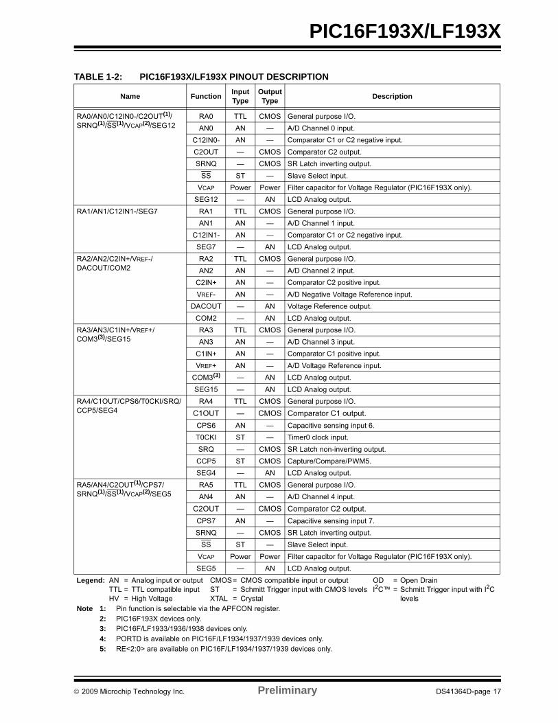
TABLE 1-2: PIC16F193X/LF193X PINOUT DESCRIPTION
Name FunctionInput Type
Output Type
Description
RA0/AN0/C12IN0-/C2OUT(1)/SRNQ(1)/SS(1)/VCAP(2)/SEG12
RA0 TTL CMOS General purpose I/O.
AN0 AN — A/D Channel 0 input.
C12IN0- AN — Comparator C1 or C2 negative input.
C2OUT — CMOS Comparator C2 output.
SRNQ — CMOS SR Latch inverting output.
SS ST — Slave Select input.
VCAP Power Power Filter capacitor for Voltage Regulator (PIC16F193X only).
SEG12 — AN LCD Analog output.
RA1/AN1/C12IN1-/SEG7 RA1 TTL CMOS General purpose I/O.
AN1 AN — A/D Channel 1 input.
C12IN1- AN — Comparator C1 or C2 negative input.
SEG7 — AN LCD Analog output.
RA2/AN2/C2IN+/VREF-/DACOUT/COM2
RA2 TTL CMOS General purpose I/O.
AN2 AN — A/D Channel 2 input.
C2IN+ AN — Comparator C2 positive input.
VREF- AN — A/D Negative Voltage Reference input.
DACOUT — AN Voltage Reference output.
COM2 — AN LCD Analog output.
RA3/AN3/C1IN+/VREF+/COM3(3)/SEG15
RA3 TTL CMOS General purpose I/O.
AN3 AN — A/D Channel 3 input.
C1IN+ AN — Comparator C1 positive input.
VREF+ AN — A/D Voltage Reference input.
COM3(3) — AN LCD Analog output.
SEG15 — AN LCD Analog output.
RA4/C1OUT/CPS6/T0CKI/SRQ/CCP5/SEG4
RA4 TTL CMOS General purpose I/O.
C1OUT — CMOS Comparator C1 output.
CPS6 AN — Capacitive sensing input 6.
T0CKI ST — Timer0 clock input.
SRQ — CMOS SR Latch non-inverting output.
CCP5 ST CMOS Capture/Compare/PWM5.
SEG4 — AN LCD Analog output.
RA5/AN4/C2OUT(1)/CPS7/SRNQ(1)/SS(1)/VCAP(2)/SEG5
RA5 TTL CMOS General purpose I/O.
AN4 AN — A/D Channel 4 input.
C2OUT — CMOS Comparator C2 output.
CPS7 AN — Capacitive sensing input 7.
SRNQ — CMOS SR Latch inverting output.
SS ST — Slave Select input.
VCAP Power Power Filter capacitor for Voltage Regulator (PIC16F193X only).
SEG5 — AN LCD Analog output.
Legend: AN = Analog input or output CMOS= CMOS compatible input or output OD = Open DrainTTL = TTL compatible input ST = Schmitt Trigger input with CMOS levels I2C™ = Schmitt Trigger input with I2C HV = High Voltage XTAL = Crystal levels
Note 1: Pin function is selectable via the APFCON register.2: PIC16F193X devices only.3: PIC16F/LF1933/1936/1938 devices only.4: PORTD is available on PIC16F/LF1934/1937/1939 devices only.5: RE<2:0> are available on PIC16F/LF1934/1937/1939 devices only.
2009 Microchip Technology Inc. Preliminary DS41364D-page 17

PIC16F193X/LF193X
RA6/OSC2/CLKOUT/VCAP(2)/SEG1
RA6 TTL CMOS General purpose I/O.
OSC2 — XTAL Crystal/Resonator (LP, XT, HS modes).
CLKOUT — CMOS FOSC/4 output.
VCAP Power Power Filter capacitor for Voltage Regulator (PIC16F193X only).
SEG1 — AN LCD Analog output.
RA7/OSC1/CLKIN/SEG2 RA7 TTL CMOS General purpose I/O.
OSC1 XTAL — Crystal/Resonator (LP, XT, HS modes).
CLKIN CMOS — External clock input (EC mode).
SEG2 — AN LCD Analog output.
RB0/AN12/CPS0/CCP4/SRI/INT/SEG0
RB0 TTL CMOS General purpose I/O. Individually controlled interrupt-on-change. Individually enabled pull-up.
AN12 AN — A/D Channel 12 input.
CPS0 AN — Capacitive sensing input 0.
CCP4 ST CMOS Capture/Compare/PWM4.
SRI — ST SR Latch input.
INT ST — External interrupt.
SEG0 — AN LCD analog output.
RB1/AN10/C12IN3-/CPS1/P1C/VLCD1
RB1 TTL CMOS General purpose I/O. Individually controlled interrupt-on-change. Individually enabled pull-up.
AN10 AN — A/D Channel 10 input.
C12IN3- AN — Comparator C1 or C2 negative input.
CPS1 AN — Capacitive sensing input 1.
P1C — CMOS PWM output.
VLCD1 AN — LCD analog input.
RB2/AN8/CPS2/P1B/VLCD2 RB2 TTL CMOS General purpose I/O. Individually controlled interrupt-on-change. Individually enabled pull-up.
AN8 AN — A/D Channel 8 input.
CPS2 AN — Capacitive sensing input 2.
P1B — CMOS PWM output.
VLCD2 AN — LCD analog input.
RB3/AN9/C12IN2-/CPS3/CCP2(1)/P2A(1)/VLCD3
RB3 TTL CMOS General purpose I/O. Individually controlled interrupt-on-change. Individually enabled pull-up.
AN9 AN — A/D Channel 9 input.
C12IN2- AN — Comparator C1 or C2 negative input.
CPS3 AN — Capacitive sensing input 3.
CCP2 ST CMOS Capture/Compare/PWM2.
P2A — CMOS PWM output.
VLCD3 AN — LCD analog input.
TABLE 1-2: PIC16F193X/LF193X PINOUT DESCRIPTION (CONTINUED)
Name FunctionInput Type
Output Type
Description
Legend: AN = Analog input or output CMOS= CMOS compatible input or output OD = Open DrainTTL = TTL compatible input ST = Schmitt Trigger input with CMOS levels I2C™ = Schmitt Trigger input with I2C HV = High Voltage XTAL = Crystal levels
Note 1: Pin function is selectable via the APFCON register.2: PIC16F193X devices only.3: PIC16F/LF1933/1936/1938 devices only.4: PORTD is available on PIC16F/LF1934/1937/1939 devices only.5: RE<2:0> are available on PIC16F/LF1934/1937/1939 devices only.
DS41364D-page 18 Preliminary 2009 Microchip Technology Inc.

PIC16F193X/LF193X
RB4/AN11/CPS4/P1D/COM0 RB4 TTL CMOS General purpose I/O. Individually controlled interrupt-on-change. Individually enabled pull-up.
AN11 AN — A/D Channel 11 input.
CPS4 AN — Capacitive sensing input 4.
P1D — CMOS PWM output.
COM0 — AN LCD Analog output.
RB5/AN13/CPS5/P2B/CCP3(1)/P3A(1)/T1G(1)/COM1
RB5 TTL CMOS General purpose I/O. Individually controlled interrupt-on-change. Individually enabled pull-up.
AN13 AN — A/D Channel 13 input.
CPS5 AN — Capacitive sensing input 5.
P2B — CMOS PWM output.
CCP3 ST CMOS Capture/Compare/PWM3.
P3A — CMOS PWM output.
T1G ST — Timer1 Gate input.
COM1 — AN LCD Analog output.
RB6/ICSPCLK/ICDCLK/SEG14 RB6 TTL CMOS General purpose I/O. Individually controlled interrupt-on-change. Individually enabled pull-up.
ICSPCLK ST — Serial Programming Clock.
ICDCLK ST — In-Circuit Debug Clock.
SEG14 — AN LCD Analog output.
RB7/ICSPDAT/ICDDAT/SEG13 RB7 TTL CMOS General purpose I/O. Individually controlled interrupt-on-change. Individually enabled pull-up.
ICSPDAT ST CMOS ICSP™ Data I/O.
ICDDAT ST CMOS In-Circuit Data I/O.
SEG13 — AN LCD Analog output.
RC0/T1OSO/T1CKI/P2B(1) RC0 ST CMOS General purpose I/O.
T1OSO XTAL XTAL Timer1 oscillator connection.
T1CKI ST — Timer1 clock input.
P2B — CMOS PWM output.
RC1/T1OSI/CCP2(1)/P2A(1) RC1 ST CMOS General purpose I/O.
T1OSI XTAL XTAL Timer1 oscillator connection.
CCP2 ST CMOS Capture/Compare/PWM2.
P2A — CMOS PWM output.
RC2/CCP1/P1A/SEG3 RC2 ST CMOS General purpose I/O.
CCP1 ST CMOS Capture/Compare/PWM1.
P1A — CMOS PWM output.
SEG3 — AN LCD Analog output.
RC3/SCK/SCL/SEG6 RC3 ST CMOS General purpose I/O.
SCK ST CMOS SPI clock.
SCL I2C OD I2C™ clock.
SEG6 — AN LCD Analog output.
TABLE 1-2: PIC16F193X/LF193X PINOUT DESCRIPTION (CONTINUED)
Name FunctionInput Type
Output Type
Description
Legend: AN = Analog input or output CMOS= CMOS compatible input or output OD = Open DrainTTL = TTL compatible input ST = Schmitt Trigger input with CMOS levels I2C™ = Schmitt Trigger input with I2C HV = High Voltage XTAL = Crystal levels
Note 1: Pin function is selectable via the APFCON register.2: PIC16F193X devices only.3: PIC16F/LF1933/1936/1938 devices only.4: PORTD is available on PIC16F/LF1934/1937/1939 devices only.5: RE<2:0> are available on PIC16F/LF1934/1937/1939 devices only.
2009 Microchip Technology Inc. Preliminary DS41364D-page 19
PIC16F193X/LF193X
RC4/SDI/SDA/T1G(1)/SEG11 RC4 ST CMOS General purpose I/O.
SDI ST — SPI data input.
SDA I2C OD I2C™ data input/output.
T1G ST — Timer1 Gate input.
SEG11 — AN LCD Analog output.
RC5/SDO/SEG10 RC5 ST CMOS General purpose I/O.
SDO — CMOS SPI data output.
SEG10 — AN LCD Analog output.
RC6/TX/CK/CCP3/P3A/SEG9 RC6 ST CMOS General purpose I/O.
TX — CMOS USART asynchronous transmit.
CK ST CMOS USART synchronous clock.
CCP3 ST CMOS Capture/Compare/PWM3.
P3A — CMOS PWM output.
SEG9 — AN LCD Analog output.
RC7/RX/DT/P3B/SEG8 RC7 ST CMOS General purpose I/O.
RX ST — USART asynchronous input.
DT ST CMOS USART synchronous data.
P3B — CMOS PWM output.
SEG8 — AN LCD Analog output.
RD0(4)/CPS8/COM3 RD0 ST CMOS General purpose I/O.
CPS8 AN — Capacitive sensing input 8.
COM3 — AN LCD analog output.
RD1(4)/CPS9/CCP4 RD1 ST CMOS General purpose I/O.
CPS9 AN — Capacitive sensing input 9.
CCP4 ST CMOS Capture/Compare/PWM4.
RD2(4)/CPS10/P2B RD2 ST CMOS General purpose I/O.
CPS10 AN — Capacitive sensing input 10.
P2B — CMOS PWM output.
RD3(4)/CPS11/P2C/SEG16 RD3 ST CMOS General purpose I/O.
CPS11 AN — Capacitive sensing input 11.
P2C — CMOS PWM output.
SEG16 — AN LCD analog output.
RD4(4)/CPS12/P2D/SEG17 RD4 ST CMOS General purpose I/O.
CPS12 AN — Capacitive sensing input 12.
P2D — CMOS PWM output.
SEG17 — AN LCD analog output.
RD5(4)/CPS13/P1B/SEG18 RD5 ST CMOS General purpose I/O.
CPS13 AN — Capacitive sensing input 13.
P1D — CMOS PWM output.
SEG18 — AN LCD analog output.
TABLE 1-2: PIC16F193X/LF193X PINOUT DESCRIPTION (CONTINUED)
Name FunctionInput Type
Output Type
Description
Legend: AN = Analog input or output CMOS= CMOS compatible input or output OD = Open DrainTTL = TTL compatible input ST = Schmitt Trigger input with CMOS levels I2C™ = Schmitt Trigger input with I2C HV = High Voltage XTAL = Crystal levels
Note 1: Pin function is selectable via the APFCON register.2: PIC16F193X devices only.3: PIC16F/LF1933/1936/1938 devices only.4: PORTD is available on PIC16F/LF1934/1937/1939 devices only.5: RE<2:0> are available on PIC16F/LF1934/1937/1939 devices only.
DS41364D-page 20 Preliminary 2009 Microchip Technology Inc.
PIC16F193X/LF193X
RD6(4)/CPS14/P1C/SEG19 RD6 ST CMOS General purpose I/O.
CPS14 AN — Capacitive sensing input 14.
P1C — CMOS PWM output.
SEG19 — AN LCD analog output.
RD7(4)/CPS15/P1D/SEG20 RD7 ST CMOS General purpose I/O.
CPS15 AN — Capacitive sensing input 15.
P1D — CMOS PWM output.
SEG20 — AN LCD analog output.
RE0(5)/AN5/P3A(1)/CCP3(1)/SEG21
RE0 ST CMOS General purpose I/O.
AN5 AN — A/D Channel 5 input.
P3A — CMOS PWM output.
CCP3 ST CMOS Capture/Compare/PWM3.
SEG21 — AN LCD analog output.
RE1(5)/AN6/P3B/SEG22 RE1 ST CMOS General purpose I/O.
AN6 AN — A/D Channel 6 input.
P3B — CMOS PWM output.
SEG22 — AN LCD analog output.
RE2(5)/AN7/CCP5/SEG23 RE2 ST CMOS General purpose I/O.
AN7 AN — A/D Channel 7 input.
CCP5 ST CMOS Capture/Compare/PWM5.
SEG23 — AN LCD analog output.
RE3/MCLR/VPP RE3 TTL — General purpose input.
MCLR ST — Master Clear with internal pull-up.
VPP HV — Programming voltage.
VDD VDD Power — Positive supply.
VSS VSS Power — Ground reference.
TABLE 1-2: PIC16F193X/LF193X PINOUT DESCRIPTION (CONTINUED)
Name FunctionInput Type
Output Type
Description
Legend: AN = Analog input or output CMOS= CMOS compatible input or output OD = Open DrainTTL = TTL compatible input ST = Schmitt Trigger input with CMOS levels I2C™ = Schmitt Trigger input with I2C HV = High Voltage XTAL = Crystal levels
Note 1: Pin function is selectable via the APFCON register.2: PIC16F193X devices only.3: PIC16F/LF1933/1936/1938 devices only.4: PORTD is available on PIC16F/LF1934/1937/1939 devices only.5: RE<2:0> are available on PIC16F/LF1934/1937/1939 devices only.
2009 Microchip Technology Inc. Preliminary DS41364D-page 21

PIC16F193X/LF193X
NOTES:
DS41364D-page 22 Preliminary 2009 Microchip Technology Inc.
PIC16F193X/LF193X
2.0 ENHANCED MID-RANGE CPU
This family of devices contain an enhanced mid-range8-bit CPU core. The CPU has 49 instructions. Interruptcapability includes automatic context saving. Thehardware stack is 16 levels deep and has Overflow andUnderflow Reset capability. Direct, indirect, and relativeaddressing modes are available. Two File SelectRegisters (FSRs) provide the ability to read programand data memory.
• Automatic Interrupt Context Saving
• 16-level Stack with Overflow and Underflow
• File Select Registers
• Instruction Set
2.1 Automatic Interrupt Context Saving
During interrupts, certain registers are automaticallysaved in shadow registers and restored when returningfrom the interrupt. This saves stack space and usercode. See Section 7.5 “Automatic Context Saving”,for more information.
2.2 16-level Stack with Overflow and Underflow
These devices have an external stack memory 15 bitswide and 16 words deep. A Stack Overflow or Under-flow will set the appropriate bit (STKOVF or STKUNF)in the PCON register, and if enabled will cause a soft-ware Reset. See section Section 3.4 “Stack” for moredetails.
2.3 File Select Registers
There are two 16-bit File Select Registers (FSR). FSRscan access all file registers and program memory,which allows one data pointer for all memory. When anFSR points to program memory, there is 1 additionalinstruction cycle in instructions using INDF to allow thedata to be fetched. General purpose memory can nowalso be addressed linearly, providing the ability toaccess contiguous data larger than 80 bytes. There arealso new instructions to support the FSRs. SeeSection 3.5 “Indirect Addressing” for more details.
2.4 Instruction Set
There are 49 instructions for the enhanced mid-rangeCPU to support the features of the CPU. SeeSection 28.0 “Instruction Set Summary” for moredetails.
2009 Microchip Technology Inc. Preliminary DS41364D-page 23

PIC16F193X/LF193X
FIGURE 2-1: CORE BLOCK DIAGRAM
Data Bus 8
14ProgramBus
Instruction reg
Program Counter
8 Level Stack(13-bit)
Direct Addr 7
9
Addr MUX
FSR reg
STATUS reg
MUX
ALU
Power-upTimer
OscillatorStart-up Timer
Power-onReset
WatchdogTimer
InstructionDecode &
Control
TimingGeneration
OSC1/CLKIN
OSC2/CLKOUT
VDD
8
8
Brown-outReset
12
3
VSS
InternalOscillator
Block
Configuration
Data Bus 8
14ProgramBus
Instruction reg
Program Counter
8 Level Stack(13-bit)
Direct Addr 7
Addr MUX
FSR reg
STATUS reg
MUX
ALU
W reg
InstructionDecode &
Control
TimingGeneration
VDD
8
8
3
VSS
InternalOscillator
Block
Configuration15 Data Bus 8
14ProgramBus
Instruction Reg
Program Counter
16-Level Stack(15-bit)
Direct Addr 7
RAM Addr
Addr MUX
IndirectAddr
FSR0 Reg
STATUS Reg
MUX
ALU
InstructionDecode and
Control
TimingGeneration
VDD
8
8
3
VSS
InternalOscillator
Block
Configuration
Flash
ProgramMemory
RAM
FSR regFSR regFSR1 Reg
15
15
MU
X15
Program Memory
Read (PMR)
12
DS41364D-page 24 Preliminary 2009 Microchip Technology Inc.

PIC16F193X/LF193X
3.0 MEMORY ORGANIZATION
There are three types of memory inPIC16F193X/LF193X devices: Data Memory, ProgramMemory and Data EEPROM Memory(1).
• Program Memory
• Data Memory
- Core Registers
- Special Function Registers
- General Purpose RAM
- Common RAM
- Device Memory Maps
- Special Function Registers Summary
• Data EEPROM memory(1)
The following features are associated with access andcontrol of program memory and data memory:
• PCL and PCLATH
• Stack
• Indirect Addressing
3.1 Program Memory Organization
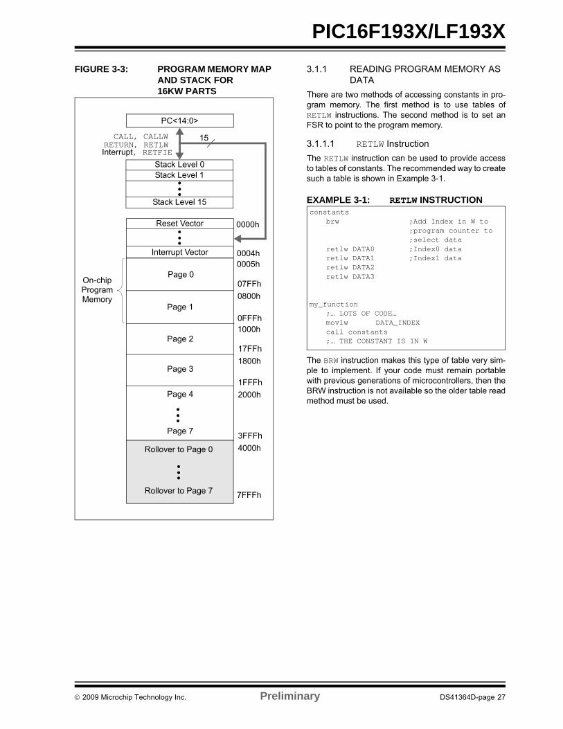
The enhanced mid-range core has a 15-bit programcounter capable of addressing 32K x 14 programmemory space. Table 3-1 shows the memory sizesimplemented for the PIC16F193X/LF193X family.Accessing a location above these boundaries will causea wrap-around within the implemented memory space.The Reset vector is at 0000h and the interrupt vector isat 0004h (see Figures 3-1, 3-2 and 3-3).
Note 1: The Data EEPROM Memory and themethod to access Flash memory throughthe EECON registers is described inSection 11.0 “Data EEPROM and FlashProgram Memory Control”.
TABLE 3-1: DEVICE SIZES AND ADDRESSES
Device Program Memory Space (Words) Last Program Memory Address
PIC16F1933/PIC16LF1933 4,096 0FFFh
PIC16F1934/PIC16LF1934 4,096 0FFFh
PIC16F1936/PIC16LF1936 8,192 1FFFh
PIC16F1937/PIC16LF1937 8,192 1FFFh
PIC16F1938/PIC16LF1938 16,384 3FFFh
PIC16F1939/PIC16LF1939 16,384 3FFFh
2009 Microchip Technology Inc. Preliminary DS41364D-page 25
PIC16F193X/LF193X
FIGURE 3-1: PROGRAM MEMORY MAP AND STACK FOR 4KW PARTS
FIGURE 3-2: PROGRAM MEMORY MAP AND STACK FOR 8KW PARTS
PC<14:0>
15
0000h
0004h
Stack Level 0
Stack Level 15
Reset Vector
Interrupt Vector
CALL, CALLW RETURN, RETLW
Stack Level 1
0005h
On-chipProgramMemory
Page 007FFh
Rollover to Page 0
0800h
0FFFh1000h
7FFFh
Page 1
Rollover to Page 1
Interrupt, RETFIE
PC<14:0>
15
0000h
0004h
Stack Level 0
Stack Level 15
Reset Vector
Interrupt Vector
Stack Level 1
0005h
On-chipProgramMemory
Page 007FFh
Rollover to Page 0
0800h
0FFFh1000h
7FFFh
Page 1
Rollover to Page 3
Page 2
Page 3
17FFh
1800h
1FFFh
2000h
CALL, CALLW RETURN, RETLW
Interrupt, RETFIE
DS41364D-page 26 Preliminary 2009 Microchip Technology Inc.
PIC16F193X/LF193X
FIGURE 3-3: PROGRAM MEMORY MAP AND STACK FOR 16KW PARTS
3.1.1 READING PROGRAM MEMORY AS DATA
There are two methods of accessing constants in pro-gram memory. The first method is to use tables ofRETLW instructions. The second method is to set anFSR to point to the program memory.
3.1.1.1 RETLW Instruction
The RETLW instruction can be used to provide accessto tables of constants. The recommended way to createsuch a table is shown in Example 3-1.
EXAMPLE 3-1: RETLW INSTRUCTION
The BRW instruction makes this type of table very sim-ple to implement. If your code must remain portablewith previous generations of microcontrollers, then theBRW instruction is not available so the older table readmethod must be used.
PC<14:0>
15
0000h
0004h
Stack Level 0
Stack Level 15
Reset Vector
Interrupt Vector
Stack Level 1
0005h
On-chipProgramMemory
Page 007FFh
Rollover to Page 0
0800h
0FFFh1000h
7FFFh
Page 1
Rollover to Page 7
Page 2
Page 3
17FFh
1800h
1FFFh
2000hPage 4
Page 73FFFh
4000h
CALL, CALLW RETURN, RETLW
Interrupt, RETFIE
constantsbrw ;Add Index in W to
;program counter to;select data
retlw DATA0 ;Index0 dataretlw DATA1 ;Index1 dataretlw DATA2retlw DATA3
my_function;… LOTS OF CODE…movlw DATA_INDEXcall constants;… THE CONSTANT IS IN W
2009 Microchip Technology Inc. Preliminary DS41364D-page 27

PIC16F193X/LF193X
3.1.1.2 Indirect Read with FSR
The program memory can be accessed as data by set-ting bit 7 of the FSRxH register and reading the match-ing INDFx register. The MOVIW instruction will place thelower 8 bits of the addressed word in the W register.Writes to the program memory cannot be performed viathe INDF registers. Instructions that access the pro-gram memory via the FSR require one extra instructioncycle to complete. Example 3-2 demonstrates access-ing the program memory via an FSR.
The HIGH directive will set bit<7> if a label points to alocation in program memory.
EXAMPLE 3-2: ACCESSING PROGRAM MEMORY VIA FSR
3.2 Data Memory Organization
The data memory is partitioned in 32 memory bankswith 128 bytes in a bank. Each bank consists of(Figure 3-4):
• 12 core registers
• 20 Special Function Registers (SFR)
• Up to 80 bytes of General Purpose RAM (GPR)
• 16 bytes of common RAM
The active bank is selected by writing the bank numberinto the Bank Select Register (BSR). Unimplementedmemory will read as ‘0’. All data memory can beaccessed either directly (via instructions that use thefile registers) or indirectly via the two File SelectRegisters (FSR). See Section 3.5 “IndirectAddressing” for more information.
3.2.1 CORE REGISTERS
The core registers contain the registers that directlyaffect the basic operation of the PIC16F193X/LF193X.These registers are listed below:
• INDF0
• INDF1
• PCL
• STATUS
• FSR0 Low
• FSR0 High
• FSR1 Low
• FSR1 High
• BSR
• WREG
• PCLATH
• INTCON
constantsretlw DATA0 ;Index0 dataretlw DATA1 ;Index1 dataretlw DATA2retlw DATA3
my_function;… LOTS OF CODE…movlw LOW constantsmovwf FSR1Lmovlw HIGH constantsmovwf FSR1Hmoviw 0[INDF1]
;THE PROGRAM MEMORY IS IN W
Note: The core registers are the first 12addresses of every data memory bank.
DS41364D-page 28 Preliminary 2009 Microchip Technology Inc.
PIC16F193X/LF193X
3.2.1.1 STATUS Register
The STATUS register, shown in Register 3-1, contains:
• the arithmetic status of the ALU
• the Reset status
The STATUS register can be the destination for anyinstruction, like any other register. If the STATUSregister is the destination for an instruction that affectsthe Z, DC or C bits, then the write to these three bits isdisabled. These bits are set or cleared according to thedevice logic. Furthermore, the TO and PD bits are notwritable. Therefore, the result of an instruction with theSTATUS register as destination may be different thanintended.
For example, CLRF STATUS will clear the upper threebits and set the Z bit. This leaves the STATUS registeras ‘000u u1uu’ (where u = unchanged).
It is recommended, therefore, that only BCF, BSF,SWAPF and MOVWF instructions are used to alter theSTATUS register, because these instructions do notaffect any Status bits. For other instructions notaffecting any Status bits (Refer to Section 28.0“Instruction Set Summary”).
Note 1: The C and DC bits operate as Borrow andDigit Borrow out bits, respectively, insubtraction.
REGISTER 3-1: STATUS: STATUS REGISTER
U-0 U-0 U-0 R-1/q R-1/q R/W-0/u R/W-0/u R/W-0/u
— — — TO PD Z DC(1) C(1)
bit 7 bit 0
Legend:
R = Readable bit W = Writable bit U = Unimplemented bit, read as ‘0’
u = Bit is unchanged x = Bit is unknown -n/n = Value at POR and BOR/Value at all other Resets
‘1’ = Bit is set ‘0’ = Bit is cleared q = Value depends on condition
bit 7-5 Unimplemented: Read as ‘0’
bit 4 TO: Time-out bit
1 = After power-up, CLRWDT instruction or SLEEP instruction0 = A WDT time-out occurred
bit 3 PD: Power-down bit
1 = After power-up or by the CLRWDT instruction0 = By execution of the SLEEP instruction
bit 2 Z: Zero bit
1 = The result of an arithmetic or logic operation is zero0 = The result of an arithmetic or logic operation is not zero
bit 1 DC: Digit Carry/Digit Borrow bit (ADDWF, ADDLW,SUBLW,SUBWF instructions)(1)
1 = A carry-out from the 4th low-order bit of the result occurred0 = No carry-out from the 4th low-order bit of the result
bit 0 C: Carry/Borrow bit(1) (ADDWF, ADDLW, SUBLW, SUBWF instructions)(1)
1 = A carry-out from the Most Significant bit of the result occurred0 = No carry-out from the Most Significant bit of the result occurred
Note 1: For Borrow, the polarity is reversed. A subtraction is executed by adding the two’s complement of the second operand. For rotate (RRF, RLF) instructions, this bit is loaded with either the high-order or low-order bit of the source register.
2009 Microchip Technology Inc. Preliminary DS41364D-page 29
PIC16F193X/LF193X
3.2.2 SPECIAL FUNCTION REGISTER
The Special Function Registers are registers used bythe application to control the desired operation ofperipheral functions in the device. The registers asso-ciated with the operation of the peripherals aredescribed in the appropriate peripheral chapter of thisdata sheet.
3.2.3 GENERAL PURPOSE RAM
There are up to 80 bytes of GPR in each data memorybank.
3.2.3.1 Linear Access to GPR
The general purpose RAM can be accessed in anon-banked method via the FSRs. This can simplifyaccess to large memory structures. See Section 3.5.2“Linear Data Memory” for more information.
3.2.4 COMMON RAM
There are 16 bytes of common RAM accessible from allbanks.
FIGURE 3-4: BANKED MEMORY PARTITIONING
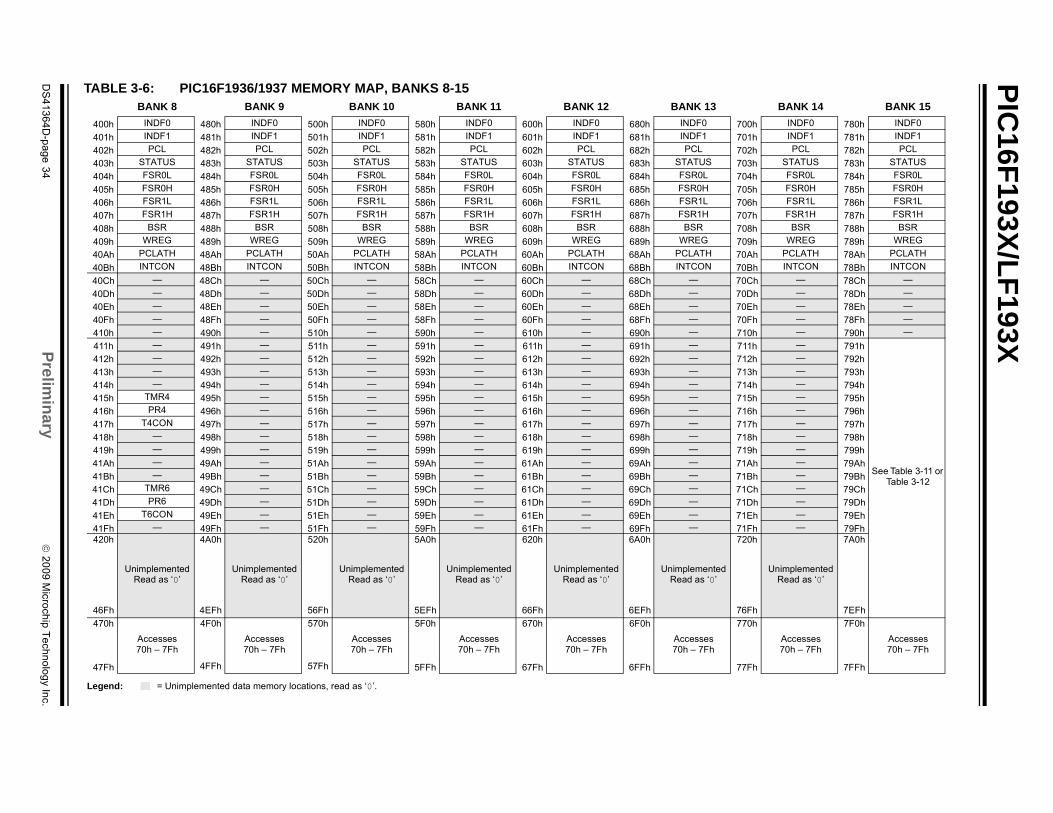
3.2.5 DEVICE MEMORY MAPS
The memory maps for the device family are as shownin Table 3-2.
0Bh0Ch
1Fh
20h
6Fh70h
7Fh
00h
Common RAM(16 bytes)
General Purpose RAM(80 bytes maximum)
Core Registers(12 bytes)
Special Function Registers(20 bytes maximum)
Memory Region7-bit Bank Offset
TABLE 3-2: MEMORY MAP TABLES
Device Banks Table No.
PIC16F1933PIC16LF1933
0-7 Table 3-3
8-15 Table 3-4,Table 3-11
16-23 Table 3-9
23-31 Table 3-10, Table 3-13
PIC16F1934PIC16LF1934
0-7 Table 3-3
8-15 Table 3-4,Table 3-12
16-23 Table 3-9
23-31 Table 3-10, Table 3-13
PIC16F1936PIC16LF1936
0-7 Table 3-5
8-15 Table 3-6, Table 3-11
16-23 Table 3-9
23-31 Table 3-10, Table 3-13
PIC16F1937PIC16LF1937
0-7 Table 3-5
8-15 Table 3-6, Table 3-12
16-23 Table 3-9
23-31 Table 3-10, Table 3-13
PIC16F1938PIC16LF1938
0-7 Table 3-7
8-15 Table 3-8, Table 3-11
16-23 Table 3-9
23-31 Table 3-10, Table 3-13
PIC16F1939PIC16LF1939
0-7 Table 3-7
8-15 Table 3-8, Table 3-12
16-23 Table 3-9
23-31 Table 3-10, Table 3-13
DS41364D-page 30 Preliminary 2009 Microchip Technology Inc.

PIC
16F193X
/LF
193X
DS
41
36
4D
-pa
ge
31
Prelim
inary
2
00
9 M
icroch
ip T
ech
no
log
y Inc.
BANK 6 BANK 7
300h INDF0 380h INDF0
301h INDF1 381h INDF1
302h PCL 382h PCL
303h STATUS 383h STATUS
304h FSR0L 384h FSR0L
305h FSR0H 385h FSR0H
306h FSR1L 386h FSR1L
307h FSR1H 387h FSR1H
308h BSR 388h BSR
309h WREG 389h WREG
30Ah PCLATH 38Ah PCLATH
30Bh INTCON 38Bh INTCON
30Ch — 38Ch —
30Dh — 38Dh —
30Eh — 38Eh —
30Fh — 38Fh —
310h — 390h —
311h CCPR3L 391h —
312h CCPR3H 392h —
313h CCP3CON 393h —
314h PWM3CON 394h IOCBP
315h CCP3AS 395h IOCBN
316h PSTR3CON 396h IOCBF
317h — 397h —
318h CCPR4L 398h —
319h CCPR4H 399h —
31Ah CCP4CON 39Ah —
31Bh — 39Bh —
31Ch CCPR5L 39Ch —
31Dh CCPR5H 39Dh —
31Eh CCP5CON 39Eh —
31Fh — 39Fh —320h
UnimplementedRead as ‘0’
3A0h
UnimplementedRead as ‘0’
36Fh 3EFh
370hAccesses70h – 7Fh
3F0hAccesses70h – 7Fh
37Fh 3FFh
TABLE 3-3: PIC16F1933/1934 MEMORY MAP, BANKS 0-7
Legend: = Unimplemented data memory locations, read as ‘0’.
Note 1: Not available on PIC16F1933/1936/1938/PIC16LF1933/1936/1938.
BANK 0 BANK 1 BANK 2 BANK 3 BANK 4 BANK 5
000h INDF0 080h INDF0 100h INDF0 180h INDF0 200h INDF0 280h INDF0
001h INDF1 081h INDF1 101h INDF1 181h INDF1 201h INDF1 281h INDF1
002h PCL 082h PCL 102h PCL 182h PCL 202h PCL 282h PCL
003h STATUS 083h STATUS 103h STATUS 183h STATUS 203h STATUS 283h STATUS
004h FSR0L 084h FSR0L 104h FSR0L 184h FSR0L 204h FSR0L 284h FSR0L
005h FSR0H 085h FSR0H 105h FSR0H 185h FSR0H 205h FSR0H 285h FSR0H
006h FSR1L 086h FSR1L 106h FSR1L 186h FSR1L 206h FSR1L 286h FSR1L
007h FSR1H 087h FSR1H 107h FSR1H 187h FSR1H 207h FSR1H 287h FSR1H
008h BSR 088h BSR 108h BSR 188h BSR 208h BSR 288h BSR
009h WREG 089h WREG 109h WREG 189h WREG 209h WREG 289h WREG
00Ah PCLATH 08Ah PCLATH 10Ah PCLATH 18Ah PCLATH 20Ah PCLATH 28Ah PCLATH
00Bh INTCON 08Bh INTCON 10Bh INTCON 18Bh INTCON 20Bh INTCON 28Bh INTCON
00Ch PORTA 08Ch TRISA 10Ch LATA 18Ch ANSELA 20Ch — 28Ch —
00Dh PORTB 08Dh TRISB 10Dh LATB 18Dh ANSELB 20Dh WPUB 28Dh —
00Eh PORTC 08Eh TRISC 10Eh LATC 18Eh — 20Eh — 28Eh —
00Fh PORTD(1) 08Fh TRISD(1) 10Fh LATD(1) 18Fh ANSELD(1) 20Fh — 28Fh —
010h PORTE 090h TRISE 110h LATE(1) 190h ANSELE(1) 210h WPUE 290h —
011h PIR1 091h PIE1 111h CM1CON0 191h EEADRL 211h SSPxBUF 291h CCPR1L
012h PIR2 092h PIE2 112h CM1CON1 192h EEADRH 212h SSPxADD 292h CCPR1H
013h PIR3 093h PIE3 113h CM2CON0 193h EEDATL 213h SSPxMSK 293h CCP1CON
014h — 094h — 114h CM2CON1 194h EEDATH 214h SSPxSTAT 294h PWM1CON
015h TMR0 095h OPTION 115h CMOUT 195h EECON1 215h SSPxCON1 295h CCP1AS
016h TMR1L 096h PCON 116h BORCON 196h EECON2 216h SSPxCON2 296h PSTR1CON
017h TMR1H 097h WDTCON 117h FVRCON 197h — 217h SSPxCON3 297h —
018h T1CON 098h OSCTUNE 118h DACCON0 198h — 218h — 298h CCPR2L
019h T1GCON 099h OSCCON 119h DACCON1 199h RCREG 219h — 299h CCPR2H
01Ah TMR2 09Ah OSCSTAT 11Ah SRCON0 19Ah TXREG 21Ah — 29Ah CCP2CON
01Bh PR2 09Bh ADRESL 11Bh SRCON1 19Bh SPBRGL 21Bh — 29Bh PWM2CON
01Ch T2CON 09Ch ADRESH 11Ch — 19Ch SPBRGH 21Ch — 29Ch CCP2AS
01Dh — 09Dh ADCON0 11Dh APFCON 19Dh RCSTA 21Dh — 29Dh PSTR2CON
01Eh CPSCON0 09Eh ADCON1 11Eh — 19Eh TXSTA 21Eh — 29Eh CCPTMRS0
01Fh CPSCON1 09Fh — 11Fh — 19Fh BAUDCTR 21Fh — 29Fh CCPTMRS1020h
GeneralPurposeRegister96 Bytes
0A0h
GeneralPurposeRegister80 Bytes
120h
GeneralPurposeRegister80 Bytes
1A0h
UnimplementedRead as ‘0’
220h
UnimplementedRead as ‘0’
2A0h
UnimplementedRead as ‘0’
06Fh 0EFh 16Fh 1EFh 26Fh 2EFh070h 0F0h
Accesses70h – 7Fh
170hAccesses70h – 7Fh
1F0hAccesses70h – 7Fh
270hAccesses70h – 7Fh
2F0hAccesses70h – 7Fh
07Fh 0FFh 17Fh 1FFh 27Fh 2FFh

PIC
16F193X
/LF
193X
DS
41
36
4D
-pa
ge
32
Prelim
inary
2
00
9 M
icroch
ip T
ech
no
log
y Inc.
BANK 14 BANK 15
700h INDF0 780h INDF0
701h INDF1 781h INDF1
702h PCL 782h PCL
703h STATUS 783h STATUS
704h FSR0L 784h FSR0L
705h FSR0H 785h FSR0H
706h FSR1L 786h FSR1L
707h FSR1H 787h FSR1H
708h BSR 788h BSR
709h WREG 789h WREG
70Ah PCLATH 78Ah PCLATH
70Bh INTCON 78Bh INTCON
70Ch — 78Ch —
70Dh — 78Dh —
70Eh — 78Eh —
70Fh — 78Fh —
710h — 790h —
711h — 791h
See Table 3-11 or Table 3-12
712h — 792h
713h — 793h
714h — 794h
715h — 795h
716h — 796h
717h — 797h
718h — 798h
719h — 799h
71Ah — 79Ah
71Bh — 79Bh
71Ch — 79Ch
71Dh — 79Dh
71Eh — 79Eh
71Fh — 79Fh
d
720h
UnimplementedRead as ‘0’
7A0h
76Fh 7EFh
770h
Accesses70h – 7Fh
7F0h
Accesses70h – 7Fh
77Fh 7FFh
TABLE 3-4: PIC16F1933/1934 MEMORY MAP, BANKS 8-15
Legend: = Unimplemented data memory locations, read as ‘0’.
BANK 8 BANK 9 BANK 10 BANK 11 BANK 12 BANK 13
400h INDF0 480h INDF0 500h INDF0 580h INDF0 600h INDF0 680h INDF0
401h INDF1 481h INDF1 501h INDF1 581h INDF1 601h INDF1 681h INDF1
402h PCL 482h PCL 502h PCL 582h PCL 602h PCL 682h PCL
403h STATUS 483h STATUS 503h STATUS 583h STATUS 603h STATUS 683h STATUS
404h FSR0L 484h FSR0L 504h FSR0L 584h FSR0L 604h FSR0L 684h FSR0L
405h FSR0H 485h FSR0H 505h FSR0H 585h FSR0H 605h FSR0H 685h FSR0H
406h FSR1L 486h FSR1L 506h FSR1L 586h FSR1L 606h FSR1L 686h FSR1L
407h FSR1H 487h FSR1H 507h FSR1H 587h FSR1H 607h FSR1H 687h FSR1H
408h BSR 488h BSR 508h BSR 588h BSR 608h BSR 688h BSR
409h WREG 489h WREG 509h WREG 589h WREG 609h WREG 689h WREG
40Ah PCLATH 48Ah PCLATH 50Ah PCLATH 58Ah PCLATH 60Ah PCLATH 68Ah PCLATH
40Bh INTCON 48Bh INTCON 50Bh INTCON 58Bh INTCON 60Bh INTCON 68Bh INTCON
40Ch — 48Ch — 50Ch — 58Ch — 60Ch — 68Ch —
40Dh — 48Dh — 50Dh — 58Dh — 60Dh — 68Dh —
40Eh — 48Eh — 50Eh — 58Eh — 60Eh — 68Eh —
40Fh — 48Fh — 50Fh — 58Fh — 60Fh — 68Fh —
410h — 490h — 510h — 590h — 610h — 690h —
411h — 491h — 511h — 591h — 611h — 691h —
412h — 492h — 512h — 592h — 612h — 692h —
413h — 493h — 513h — 593h — 613h — 693h —
414h — 494h — 514h — 594h — 614h — 694h —
415h TMR4 495h — 515h — 595h — 615h — 695h —
416h PR4 496h — 516h — 596h — 616h — 696h —
417h T4CON 497h — 517h — 597h — 617h — 697h —
418h — 498h — 518h — 598h — 618h — 698h —
419h — 499h — 519h — 599h — 619h — 699h —
41Ah — 49Ah — 51Ah — 59Ah — 61Ah — 69Ah —
41Bh — 49Bh — 51Bh — 59Bh — 61Bh — 69Bh —
41Ch TMR6 49Ch — 51Ch — 59Ch — 61Ch — 69Ch —
41Dh PR6 49Dh — 51Dh — 59Dh — 61Dh — 69Dh —
41Eh T6CON 49Eh — 51Eh — 59Eh — 61Eh — 69Eh —
41Fh — 49Fh — 51Fh — 59Fh — 61Fh — 69Fh —420h
UnimplementedRead as ‘0’
4A0h
UnimplementedRead as ‘0’
520h
UnimplementedRead as ‘0’
5A0h
UnimplementedRead as ‘0’
620h
UnimplementedRead as ‘0’
6A0h
UnimplementeRead as ‘0’
46Fh 4EFh 56Fh 5EFh 66Fh 6EFh
470h
Accesses70h – 7Fh
4F0h
Accesses70h – 7Fh
570h
Accesses70h – 7Fh
5F0h
Accesses70h – 7Fh
670h
Accesses70h – 7Fh
6F0h
Accesses70h – 7Fh
47Fh 4FFh 57Fh 5FFh 67Fh 6FFh

PIC
16F193X
/LF
193X
DS
41
36
4D
-pa
ge
33
Prelim
inary
2
00
9 M
icroch
ip T
ech
no
log
y Inc.
BANK 6 BANK 7
300h INDF0 380h INDF0
301h INDF1 381h INDF1
302h PCL 382h PCL
303h STATUS 383h STATUS
304h FSR0L 384h FSR0L
305h FSR0H 385h FSR0H
306h FSR1L 386h FSR1L
307h FSR1H 387h FSR1H
308h BSR 388h BSR
309h WREG 389h WREG
30Ah PCLATH 38Ah PCLATH
30Bh INTCON 38Bh INTCON
30Ch — 38Ch —
30Dh — 38Dh —
30Eh — 38Eh —
30Fh — 38Fh —
310h — 390h —
311h CCPR3L 391h —
312h CCPR3H 392h —
313h CCP3CON 393h —
314h PWM3CON 394h IOCBP
315h CCP3AS 395h IOCBN
316h PSTR3CON 396h IOCBF
317h — 397h —
318h CCPR4L 398h —
319h CCPR4H 399h —
31Ah CCP4CON 39Ah —
31Bh — 39Bh —
31Ch CCPR5L 39Ch —
31Dh CCPR5H 39Dh —
31Eh CCP5CON 39Eh —
31Fh — 39Fh —320h General Purpose
Register 16 Bytes
3A0h
UnimplementedRead as ‘0’
32Fh
330hUnimplemented
Read as ‘0’36Fh 3EFh
370hAccesses70h – 7Fh
3F0hAccesses70h – 7Fh
37Fh 3FFh
TABLE 3-5: PIC16F1936/1937 MEMORY MAP, BANKS 0-7
Legend: = Unimplemented data memory locations, read as ‘0’.
Note 1: Not available on PIC16F1933/1936/1938/PIC16LF1933/1936/1938.
BANK 0 BANK 1 BANK 2 BANK 3 BANK 4 BANK 5
000h INDF0 080h INDF0 100h INDF0 180h INDF0 200h INDF0 280h INDF0
001h INDF1 081h INDF1 101h INDF1 181h INDF1 201h INDF1 281h INDF1
002h PCL 082h PCL 102h PCL 182h PCL 202h PCL 282h PCL
003h STATUS 083h STATUS 103h STATUS 183h STATUS 203h STATUS 283h STATUS
004h FSR0L 084h FSR0L 104h FSR0L 184h FSR0L 204h FSR0L 284h FSR0L
005h FSR0H 085h FSR0H 105h FSR0H 185h FSR0H 205h FSR0H 285h FSR0H
006h FSR1L 086h FSR1L 106h FSR1L 186h FSR1L 206h FSR1L 286h FSR1L
007h FSR1H 087h FSR1H 107h FSR1H 187h FSR1H 207h FSR1H 287h FSR1H
008h BSR 088h BSR 108h BSR 188h BSR 208h BSR 288h BSR
009h WREG 089h WREG 109h WREG 189h WREG 209h WREG 289h WREG
00Ah PCLATH 08Ah PCLATH 10Ah PCLATH 18Ah PCLATH 20Ah PCLATH 28Ah PCLATH
00Bh INTCON 08Bh INTCON 10Bh INTCON 18Bh INTCON 20Bh INTCON 28Bh INTCON
00Ch PORTA 08Ch TRISA 10Ch LATA 18Ch ANSELA 20Ch — 28Ch —
00Dh PORTB 08Dh TRISB 10Dh LATB 18Dh ANSELB 20Dh WPUB 28Dh —
00Eh PORTC 08Eh TRISC 10Eh LATC 18Eh — 20Eh — 28Eh —
00Fh PORTD(1) 08Fh TRISD(1) 10Fh LATD(1) 18Fh ANSELD(1) 20Fh — 28Fh —
010h PORTE 090h TRISE 110h LATE(1) 190h ANSELE(1) 210h WPUE 290h —
011h PIR1 091h PIE1 111h CM1CON0 191h EEADRL 211h SSPxBUF 291h CCPR1L
012h PIR2 092h PIE2 112h CM1CON1 192h EEADRH 212h SSPxADD 292h CCPR1H
013h PIR3 093h PIE3 113h CM2CON0 193h EEDATL 213h SSPxMSK 293h CCP1CON
014h — 094h — 114h CM2CON1 194h EEDATH 214h SSPxSTAT 294h PWM1CON
015h TMR0 095h OPTION 115h CMOUT 195h EECON1 215h SSPxCON1 295h CCP1AS
016h TMR1L 096h PCON 116h BORCON 196h EECON2 216h SSPxCON2 296h PSTR1CON
017h TMR1H 097h WDTCON 117h FVRCON 197h — 217h SSPxCON3 297h —
018h T1CON 098h OSCTUNE 118h DACCON0 198h — 218h — 298h CCPR2L
019h T1GCON 099h OSCCON 119h DACCON1 199h RCREG 219h — 299h CCPR2H
01Ah TMR2 09Ah OSCSTAT 11Ah SRCON0 19Ah TXREG 21Ah — 29Ah CCP2CON
01Bh PR2 09Bh ADRESL 11Bh SRCON1 19Bh SPBRGL 21Bh — 29Bh PWM2CON
01Ch TxCON 09Ch ADRESH 11Ch — 19Ch SPBRGH 21Ch — 29Ch CCP2AS
01Dh — 09Dh ADCON0 11Dh APFCON 19Dh RCSTA 21Dh — 29Dh PSTR2CON
01Eh CPSCON0 09Eh ADCON1 11Eh — 19Eh TXSTA 21Eh — 29Eh CCPTMRS0
01Fh CPSCON1 09Fh — 11Fh — 19Fh BAUDCON 21Fh — 29Fh CCPTMRS1020h
GeneralPurposeRegister96 Bytes
0A0h
GeneralPurposeRegister80 Bytes
120h
GeneralPurposeRegister80 Bytes
1A0h
GeneralPurposeRegister80 Bytes
220h
GeneralPurposeRegister80 Bytes
2A0h
GeneralPurposeRegister80 Bytes
06Fh 0EFh 16Fh 1EFh 26Fh 2EFh070h 0F0h
Accesses70h – 7Fh
170hAccesses70h – 7Fh
1F0hAccesses70h – 7Fh
270hAccesses70h – 7Fh
2F0hAccesses70h – 7Fh
07Fh 0FFh 17Fh 1FFh 27Fh 2FFh
PIC
16F193X
/LF
193X
DS
41
36
4D
-pa
ge
34
Prelim
inary
2
00
9 M
icroch
ip T
ech
no
log
y Inc.
BANK 14 BANK 15
700h INDF0 780h INDF0
701h INDF1 781h INDF1
702h PCL 782h PCL
703h STATUS 783h STATUS
704h FSR0L 784h FSR0L
705h FSR0H 785h FSR0H
706h FSR1L 786h FSR1L
707h FSR1H 787h FSR1H
708h BSR 788h BSR
709h WREG 789h WREG
70Ah PCLATH 78Ah PCLATH
70Bh INTCON 78Bh INTCON
70Ch — 78Ch —
70Dh — 78Dh —
70Eh — 78Eh —
70Fh — 78Fh —
710h — 790h —
711h — 791h
See Table 3-11 or Table 3-12
712h — 792h
713h — 793h
714h — 794h
715h — 795h
716h — 796h
717h — 797h
718h — 798h
719h — 799h
71Ah — 79Ah
71Bh — 79Bh
71Ch — 79Ch
71Dh — 79Dh
71Eh — 79Eh
71Fh — 79Fh
d
720h
UnimplementedRead as ‘0’
7A0h
76Fh 7EFh
770h
Accesses70h – 7Fh
7F0h
Accesses70h – 7Fh
77Fh 7FFh
TABLE 3-6: PIC16F1936/1937 MEMORY MAP, BANKS 8-15
Legend: = Unimplemented data memory locations, read as ‘0’.
BANK 8 BANK 9 BANK 10 BANK 11 BANK 12 BANK 13
400h INDF0 480h INDF0 500h INDF0 580h INDF0 600h INDF0 680h INDF0
401h INDF1 481h INDF1 501h INDF1 581h INDF1 601h INDF1 681h INDF1
402h PCL 482h PCL 502h PCL 582h PCL 602h PCL 682h PCL
403h STATUS 483h STATUS 503h STATUS 583h STATUS 603h STATUS 683h STATUS
404h FSR0L 484h FSR0L 504h FSR0L 584h FSR0L 604h FSR0L 684h FSR0L
405h FSR0H 485h FSR0H 505h FSR0H 585h FSR0H 605h FSR0H 685h FSR0H
406h FSR1L 486h FSR1L 506h FSR1L 586h FSR1L 606h FSR1L 686h FSR1L
407h FSR1H 487h FSR1H 507h FSR1H 587h FSR1H 607h FSR1H 687h FSR1H
408h BSR 488h BSR 508h BSR 588h BSR 608h BSR 688h BSR
409h WREG 489h WREG 509h WREG 589h WREG 609h WREG 689h WREG
40Ah PCLATH 48Ah PCLATH 50Ah PCLATH 58Ah PCLATH 60Ah PCLATH 68Ah PCLATH
40Bh INTCON 48Bh INTCON 50Bh INTCON 58Bh INTCON 60Bh INTCON 68Bh INTCON
40Ch — 48Ch — 50Ch — 58Ch — 60Ch — 68Ch —
40Dh — 48Dh — 50Dh — 58Dh — 60Dh — 68Dh —
40Eh — 48Eh — 50Eh — 58Eh — 60Eh — 68Eh —
40Fh — 48Fh — 50Fh — 58Fh — 60Fh — 68Fh —
410h — 490h — 510h — 590h — 610h — 690h —
411h — 491h — 511h — 591h — 611h — 691h —
412h — 492h — 512h — 592h — 612h — 692h —
413h — 493h — 513h — 593h — 613h — 693h —
414h — 494h — 514h — 594h — 614h — 694h —
415h TMR4 495h — 515h — 595h — 615h — 695h —
416h PR4 496h — 516h — 596h — 616h — 696h —
417h T4CON 497h — 517h — 597h — 617h — 697h —
418h — 498h — 518h — 598h — 618h — 698h —
419h — 499h — 519h — 599h — 619h — 699h —
41Ah — 49Ah — 51Ah — 59Ah — 61Ah — 69Ah —
41Bh — 49Bh — 51Bh — 59Bh — 61Bh — 69Bh —
41Ch TMR6 49Ch — 51Ch — 59Ch — 61Ch — 69Ch —
41Dh PR6 49Dh — 51Dh — 59Dh — 61Dh — 69Dh —
41Eh T6CON 49Eh — 51Eh — 59Eh — 61Eh — 69Eh —
41Fh — 49Fh — 51Fh — 59Fh — 61Fh — 69Fh —420h
UnimplementedRead as ‘0’
4A0h
UnimplementedRead as ‘0’
520h
UnimplementedRead as ‘0’
5A0h
UnimplementedRead as ‘0’
620h
UnimplementedRead as ‘0’
6A0h
UnimplementeRead as ‘0’
46Fh 4EFh 56Fh 5EFh 66Fh 6EFh
470h
Accesses70h – 7Fh
4F0h
Accesses70h – 7Fh
570h
Accesses70h – 7Fh
5F0h
Accesses70h – 7Fh
670h
Accesses70h – 7Fh
6F0h
Accesses70h – 7Fh
47Fh 4FFh 57Fh 5FFh 67Fh 6FFh
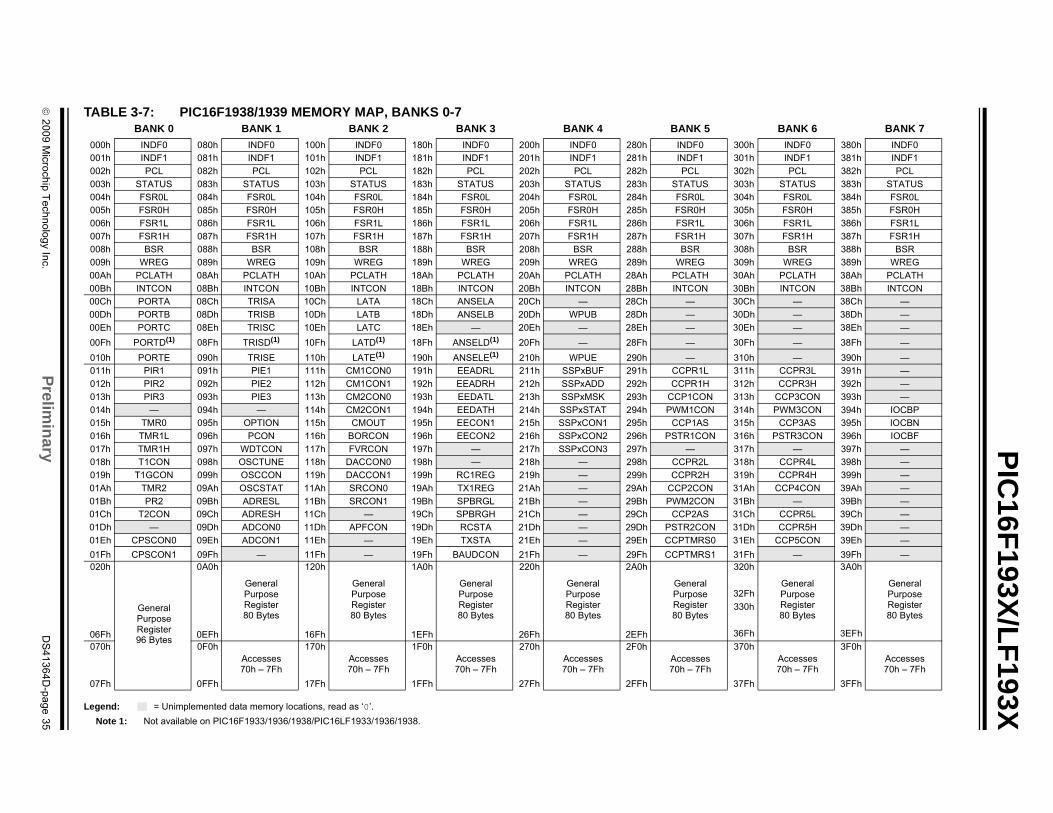
2
00
9 M
icroch
ip T
ech
no
log
y Inc.
Prelim
inary
DS
41
36
4D
-pa
ge
35
PIC
16F193X
/LF
193X
TA
Leg
N
BANK 6 BANK 7
00 0h INDF0 380h INDF0
00 1h INDF1 381h INDF1
00 2h PCL 382h PCL
00 3h STATUS 383h STATUS
00 4h FSR0L 384h FSR0L
00 5h FSR0H 385h FSR0H
00 6h FSR1L 386h FSR1L
00 7h FSR1H 387h FSR1H
00 8h BSR 388h BSR
00 9h WREG 389h WREG
00 Ah PCLATH 38Ah PCLATH
00 Bh INTCON 38Bh INTCON
00 Ch — 38Ch —
00 Dh — 38Dh —
00 Eh — 38Eh —
00 Fh — 38Fh —
01 0h — 390h —
01 1h CCPR3L 391h —
01 2h CCPR3H 392h —
01 3h CCP3CON 393h —
01 4h PWM3CON 394h IOCBP
01 5h CCP3AS 395h IOCBN
01 6h PSTR3CON 396h IOCBF
01 7h — 397h —
01 8h CCPR4L 398h —
01 9h CCPR4H 399h —
01 Ah CCP4CON 39Ah —
01 Bh — 39Bh —
01 Ch CCPR5L 39Ch —
01 Dh CCPR5H 39Dh —
01 Eh CCP5CON 39Eh —
01 Fh — 39Fh —02 0h
GeneralPurposeRegister80 Bytes
3A0h
GeneralPurposeRegister80 Bytes
Fh
0h
06 Fh 3EFh
07 0hAccesses70h – 7Fh
3F0hAccesses70h – 7Fh
07 Fh 3FFh
BLE 3-7: PIC16F1938/1939 MEMORY MAP, BANKS 0-7
end: = Unimplemented data memory locations, read as ‘0’.
ote 1: Not available on PIC16F1933/1936/1938/PIC16LF1933/1936/1938.
BANK 0 BANK 1 BANK 2 BANK 3 BANK 4 BANK 5
0h INDF0 080h INDF0 100h INDF0 180h INDF0 200h INDF0 280h INDF0 30
1h INDF1 081h INDF1 101h INDF1 181h INDF1 201h INDF1 281h INDF1 30
2h PCL 082h PCL 102h PCL 182h PCL 202h PCL 282h PCL 30
3h STATUS 083h STATUS 103h STATUS 183h STATUS 203h STATUS 283h STATUS 30
4h FSR0L 084h FSR0L 104h FSR0L 184h FSR0L 204h FSR0L 284h FSR0L 30
5h FSR0H 085h FSR0H 105h FSR0H 185h FSR0H 205h FSR0H 285h FSR0H 30
6h FSR1L 086h FSR1L 106h FSR1L 186h FSR1L 206h FSR1L 286h FSR1L 30
7h FSR1H 087h FSR1H 107h FSR1H 187h FSR1H 207h FSR1H 287h FSR1H 30
8h BSR 088h BSR 108h BSR 188h BSR 208h BSR 288h BSR 30
9h WREG 089h WREG 109h WREG 189h WREG 209h WREG 289h WREG 30
Ah PCLATH 08Ah PCLATH 10Ah PCLATH 18Ah PCLATH 20Ah PCLATH 28Ah PCLATH 30
Bh INTCON 08Bh INTCON 10Bh INTCON 18Bh INTCON 20Bh INTCON 28Bh INTCON 30
Ch PORTA 08Ch TRISA 10Ch LATA 18Ch ANSELA 20Ch — 28Ch — 30
Dh PORTB 08Dh TRISB 10Dh LATB 18Dh ANSELB 20Dh WPUB 28Dh — 30
Eh PORTC 08Eh TRISC 10Eh LATC 18Eh — 20Eh — 28Eh — 30
Fh PORTD(1) 08Fh TRISD(1) 10Fh LATD(1) 18Fh ANSELD(1) 20Fh — 28Fh — 30
0h PORTE 090h TRISE 110h LATE(1) 190h ANSELE(1) 210h WPUE 290h — 31
1h PIR1 091h PIE1 111h CM1CON0 191h EEADRL 211h SSPxBUF 291h CCPR1L 31
2h PIR2 092h PIE2 112h CM1CON1 192h EEADRH 212h SSPxADD 292h CCPR1H 31
3h PIR3 093h PIE3 113h CM2CON0 193h EEDATL 213h SSPxMSK 293h CCP1CON 31
4h — 094h — 114h CM2CON1 194h EEDATH 214h SSPxSTAT 294h PWM1CON 31
5h TMR0 095h OPTION 115h CMOUT 195h EECON1 215h SSPxCON1 295h CCP1AS 31
6h TMR1L 096h PCON 116h BORCON 196h EECON2 216h SSPxCON2 296h PSTR1CON 31
7h TMR1H 097h WDTCON 117h FVRCON 197h — 217h SSPxCON3 297h — 31
8h T1CON 098h OSCTUNE 118h DACCON0 198h — 218h — 298h CCPR2L 31
9h T1GCON 099h OSCCON 119h DACCON1 199h RC1REG 219h — 299h CCPR2H 31
Ah TMR2 09Ah OSCSTAT 11Ah SRCON0 19Ah TX1REG 21Ah — 29Ah CCP2CON 31
Bh PR2 09Bh ADRESL 11Bh SRCON1 19Bh SPBRGL 21Bh — 29Bh PWM2CON 31
Ch T2CON 09Ch ADRESH 11Ch — 19Ch SPBRGH 21Ch — 29Ch CCP2AS 31
Dh — 09Dh ADCON0 11Dh APFCON 19Dh RCSTA 21Dh — 29Dh PSTR2CON 31
Eh CPSCON0 09Eh ADCON1 11Eh — 19Eh TXSTA 21Eh — 29Eh CCPTMRS0 31
Fh CPSCON1 09Fh — 11Fh — 19Fh BAUDCON 21Fh — 29Fh CCPTMRS1 310h
GeneralPurposeRegister96 Bytes
0A0h
GeneralPurposeRegister80 Bytes
120h
GeneralPurposeRegister80 Bytes
1A0h
GeneralPurposeRegister80 Bytes
220h
GeneralPurposeRegister80 Bytes
2A0h
GeneralPurposeRegister80 Bytes
32
32
33
Fh 0EFh 16Fh 1EFh 26Fh 2EFh 36
0h 0F0hAccesses70h – 7Fh
170hAccesses70h – 7Fh
1F0hAccesses70h – 7Fh
270hAccesses70h – 7Fh
2F0hAccesses70h – 7Fh
37
Fh 0FFh 17Fh 1FFh 27Fh 2FFh 37

PIC
16F193X
/LF
193X
DS
41
36
4D
-pa
ge
36
Prelim
inary
2
00
9 M
icroch
ip T
ech
no
log
y Inc.
BANK 14 BANK 15
700h INDF0 780h INDF0
701h INDF1 781h INDF1
702h PCL 782h PCL
703h STATUS 783h STATUS
704h FSR0L 784h FSR0L
705h FSR0H 785h FSR0H
706h FSR1L 786h FSR1L
707h FSR1H 787h FSR1H
708h BSR 788h BSR
709h WREG 789h WREG
70Ah PCLATH 78Ah PCLATH
70Bh INTCON 78Bh INTCON
70Ch — 78Ch —
70Dh — 78Dh —
70Eh — 78Eh —
70Fh — 78Fh —
710h — 790h —
711h — 791h
See Table 3-11 or Table 3-12
712h — 792h
713h — 793h
714h — 794h
715h — 795h
716h — 796h
717h — 797h
718h — 798h
719h — 799h
71Ah — 79Ah
71Bh — 79Bh
71Ch — 79Ch
71Dh — 79Dh
71Eh — 79Eh
71Fh — 79Fh
d
720h
UnimplementedRead as ‘0’
7A0h
76Fh 7EFh
770h
Accesses70h – 7Fh
7F0h
Accesses70h – 7Fh
77Fh 7FFh
TABLE 3-8: PIC16F1938/1939 MEMORY MAP, BANKS 8-15
Legend: = Unimplemented data memory locations, read as ‘0’.
BANK 8 BANK 9 BANK 10 BANK 11 BANK 12 BANK 13
400h INDF0 480h INDF0 500h INDF0 580h INDF0 600h INDF0 680h INDF0
401h INDF1 481h INDF1 501h INDF1 581h INDF1 601h INDF1 681h INDF1
402h PCL 482h PCL 502h PCL 582h PCL 602h PCL 682h PCL
403h STATUS 483h STATUS 503h STATUS 583h STATUS 603h STATUS 683h STATUS
404h FSR0L 484h FSR0L 504h FSR0L 584h FSR0L 604h FSR0L 684h FSR0L
405h FSR0H 485h FSR0H 505h FSR0H 585h FSR0H 605h FSR0H 685h FSR0H
406h FSR1L 486h FSR1L 506h FSR1L 586h FSR1L 606h FSR1L 686h FSR1L
407h FSR1H 487h FSR1H 507h FSR1H 587h FSR1H 607h FSR1H 687h FSR1H
408h BSR 488h BSR 508h BSR 588h BSR 608h BSR 688h BSR
409h WREG 489h WREG 509h WREG 589h WREG 609h WREG 689h WREG
40Ah PCLATH 48Ah PCLATH 50Ah PCLATH 58Ah PCLATH 60Ah PCLATH 68Ah PCLATH
40Bh INTCON 48Bh INTCON 50Bh INTCON 58Bh INTCON 60Bh INTCON 68Bh INTCON
40Ch — 48Ch — 50Ch — 58Ch — 60Ch — 68Ch —
40Dh — 48Dh — 50Dh — 58Dh — 60Dh — 68Dh —
40Eh — 48Eh — 50Eh — 58Eh — 60Eh — 68Eh —
40Fh — 48Fh — 50Fh — 58Fh — 60Fh — 68Fh —
410h — 490h — 510h — 590h — 610h — 690h —
411h — 491h — 511h — 591h — 611h — 691h —
412h — 492h — 512h — 592h — 612h — 692h —
413h — 493h — 513h — 593h — 613h — 693h —
414h — 494h — 514h — 594h — 614h — 694h —
415h TMR4 495h — 515h — 595h — 615h — 695h —
416h PR4 496h — 516h — 596h — 616h — 696h —
417h T4CON 497h — 517h — 597h — 617h — 697h —
418h — 498h — 518h — 598h — 618h — 698h —
419h — 499h — 519h — 599h — 619h — 699h —
41Ah — 49Ah — 51Ah — 59Ah — 61Ah — 69Ah —
41Bh — 49Bh — 51Bh — 59Bh — 61Bh — 69Bh —
41Ch TMR6 49Ch — 51Ch — 59Ch — 61Ch — 69Ch —
41Dh PR6 49Dh — 51Dh — 59Dh — 61Dh — 69Dh —
41Eh T6CON 49Eh — 51Eh — 59Eh — 61Eh — 69Eh —
41Fh — 49Fh — 51Fh — 59Fh — 61Fh — 69Fh —420h
GeneralPurposeRegister80 Bytes
4A0h
GeneralPurposeRegister80 Bytes
520h
GeneralPurposeRegister80 Bytes
5A0h
GeneralPurposeRegister80 Bytes
620h General Purpose Register 48 Bytes
6A0h
UnimplementeRead as ‘0’
UnimplementedRead as ‘0’
46Fh 4EFh 56Fh 5EFh 66Fh 6EFh
470h
Accesses70h – 7Fh
4F0h
Accesses70h – 7Fh
570h
Accesses70h – 7Fh
5F0h
Accesses70h – 7Fh
670h
Accesses70h – 7Fh
6F0h
Accesses70h – 7Fh
47Fh 4FFh 57Fh 5FFh 67Fh 6FFh

2
00
9 M
icroch
ip T
ech
no
log
y Inc.
Prelim
inary
DS
41
36
4D
-pa
ge
37
PIC
16F193X
/LF
193X
TA
Leg
BANK 22 BANK 23
80 0h INDF0 B80h INDF0
80 1h INDF1 B81h INDF1
80 2h PCL B82h PCL
80 3h STATUS B83h STATUS
80 4h FSR0L B84h FSR0L
80 5h FSR0H B85h FSR0H
80 6h FSR1L B86h FSR1L
80 7h FSR1H B87h FSR1H
80 8h BSR B88h BSR
80 9h WREG B89h WREG
80 Ah PCLATH B8Ah PCLATH
80 Bh INTCON B8Bh INTCON
80 Ch — B8Ch —
80 Dh — B8Dh —
80 Eh — B8Eh —
80 Fh — B8Fh —
81 0h — B90h —
81 1h — B91h —
81 2h — B92h —
81 3h — B93h —
81 4h — B94h —
81 5h — B95h —
81 6h — B96h —
81 7h — B97h —
81 8h — B98h —
81 9h — B99h —
81 Ah — B9Ah —
81 Bh — B9Bh —
81 Ch — B9Ch —
81 Dh — B9Dh —
81 Eh — B9Eh —
81 Fh — B9Fh —82 0h
UnimplementedRead as ‘0’
BA0h
UnimplementedRead as ‘0’
86 Fh BEFh
87 0hAccesses70h – 7Fh
BF0hAccesses70h – 7Fh
87 Fh BFFh
BLE 3-9: PIC16F193X/LF193X MEMORY MAP, BANKS 16-23
end: = Unimplemented data memory locations, read as ‘0’.
BANK 16 BANK 17 BANK 18 BANK 19 BANK 20 BANK 21
0h INDF0 880h INDF0 900h INDF0 980h INDF0 A00h INDF0 A80h INDF0 B0
1h INDF1 881h INDF1 901h INDF1 981h INDF1 A01h INDF1 A81h INDF1 B0
2h PCL 882h PCL 902h PCL 982h PCL A02h PCL A82h PCL B0
3h STATUS 883h STATUS 903h STATUS 983h STATUS A03h STATUS A83h STATUS B0
4h FSR0L 884h FSR0L 904h FSR0L 984h FSR0L A04h FSR0L A84h FSR0L B0
5h FSR0H 885h FSR0H 905h FSR0H 985h FSR0H A05h FSR0H A85h FSR0H B0
6h FSR1L 886h FSR1L 906h FSR1L 986h FSR1L A06h FSR1L A86h FSR1L B0
7h FSR1H 887h FSR1H 907h FSR1H 987h FSR1H A07h FSR1H A87h FSR1H B0
8h BSR 888h BSR 908h BSR 988h BSR A08h BSR A88h BSR B0
9h WREG 889h WREG 909h WREG 989h WREG A09h WREG A89h WREG B0
Ah PCLATH 88Ah PCLATH 90Ah PCLATH 98Ah PCLATH A0Ah PCLATH A8Ah PCLATH B0
Bh INTCON 88Bh INTCON 90Bh INTCON 98Bh INTCON A0Bh INTCON A8Bh INTCON B0
Ch — 88Ch — 90Ch — 98Ch — A0Ch — A8Ch — B0
Dh — 88Dh — 90Dh — 98Dh — A0Dh — A8Dh — B0
Eh — 88Eh — 90Eh — 98Eh — A0Eh — A8Eh — B0
Fh — 88Fh — 90Fh — 98Fh — A0Fh — A8Fh — B0
0h — 890h — 910h — 990h — A10h — A90h — B1
1h — 891h — 911h — 991h — A11h — A91h — B1
2h — 892h — 912h — 992h — A12h — A92h — B1
3h — 893h — 913h — 993h — A13h — A93h — B1
4h — 894h — 914h — 994h — A14h — A94h — B1
5h — 895h — 915h — 995h — A15h — A95h — B1
6h — 896h — 916h — 996h — A16h — A96h — B1
7h — 897h — 917h — 997h — A17h — A97h — B1
8h — 898h — 918h — 998h — A18h — A98h — B1
9h — 899h — 919h — 999h — A19h — A99h — B1
Ah — 89Ah — 91Ah — 99Ah — A1Ah — A9Ah — B1
Bh — 89Bh — 91Bh — 99Bh — A1Bh — A9Bh — B1
Ch — 89Ch — 91Ch — 99Ch — A1Ch — A9Ch — B1
Dh — 89Dh — 91Dh — 99Dh — A1Dh — A9Dh — B1
Eh — 89Eh — 91Eh — 99Eh — A1Eh — A9Eh — B1
Fh — 89Fh — 91Fh — 99Fh — A1Fh — A9Fh — B10h
UnimplementedRead as ‘0’
8A0h
UnimplementedRead as ‘0’
920h
UnimplementedRead as ‘0’
9A0h
UnimplementedRead as ‘0’
A20h
UnimplementedRead as ‘0’
AA0h
UnimplementedRead as ‘0’
B2
Fh 8EFh 96Fh 9EFh A6Fh AEFh B60h
Accesses70h – 7Fh
8F0hAccesses70h – 7Fh
970hAccesses70h – 7Fh
9F0hAccesses70h – 7Fh
A70hAccesses70h – 7Fh
AF0hAccesses70h – 7Fh
B7
Fh 8FFh 97Fh 9FFh A7Fh AFFh B7
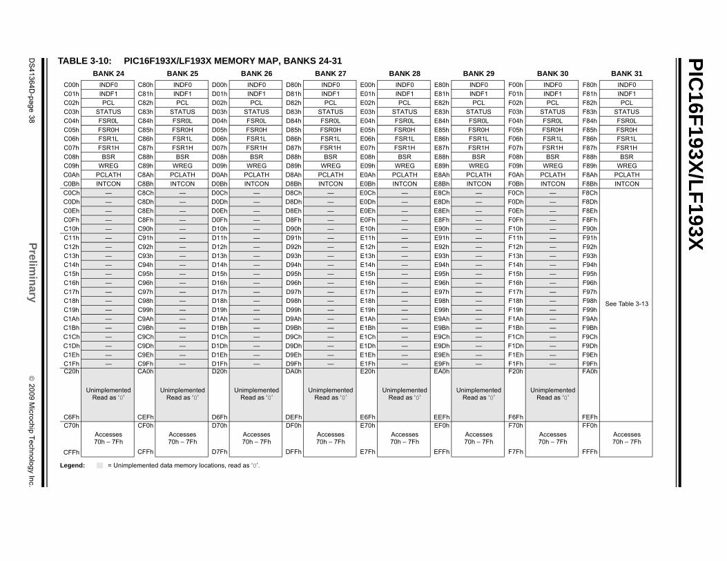
PIC
16F193X
/LF
193X
DS
41
36
4D
-pa
ge
38
Prelim
inary
2
00
9 M
icroch
ip T
ech
no
log
y Inc.
BANK 30 BANK 31
F00h INDF0 F80h INDF0
F01h INDF1 F81h INDF1
F02h PCL F82h PCL
F03h STATUS F83h STATUS
F04h FSR0L F84h FSR0L
F05h FSR0H F85h FSR0H
F06h FSR1L F86h FSR1L
F07h FSR1H F87h FSR1H
F08h BSR F88h BSR
F09h WREG F89h WREG
F0Ah PCLATH F8Ah PCLATH
F0Bh INTCON F8Bh INTCON
F0Ch — F8Ch
See Table 3-13
F0Dh — F8Dh
F0Eh — F8Eh
F0Fh — F8Fh
F10h — F90h
F11h — F91h
F12h — F92h
F13h — F93h
F14h — F94h
F15h — F95h
F16h — F96h
F17h — F97h
F18h — F98h
F19h — F99h
F1Ah — F9Ah
F1Bh — F9Bh
F1Ch — F9Ch
F1Dh — F9Dh
F1Eh — F9Eh
F1Fh — F9Fh
d
F20h
UnimplementedRead as ‘0’
FA0h
F6Fh FEFhF70h
Accesses70h – 7Fh
FF0h
Accesses70h – 7Fh
F7Fh FFFh
TABLE 3-10: PIC16F193X/LF193X MEMORY MAP, BANKS 24-31
Legend: = Unimplemented data memory locations, read as ‘0’.
BANK 24 BANK 25 BANK 26 BANK 27 BANK 28 BANK 29
C00h INDF0 C80h INDF0 D00h INDF0 D80h INDF0 E00h INDF0 E80h INDF0
C01h INDF1 C81h INDF1 D01h INDF1 D81h INDF1 E01h INDF1 E81h INDF1
C02h PCL C82h PCL D02h PCL D82h PCL E02h PCL E82h PCL
C03h STATUS C83h STATUS D03h STATUS D83h STATUS E03h STATUS E83h STATUS
C04h FSR0L C84h FSR0L D04h FSR0L D84h FSR0L E04h FSR0L E84h FSR0L
C05h FSR0H C85h FSR0H D05h FSR0H D85h FSR0H E05h FSR0H E85h FSR0H
C06h FSR1L C86h FSR1L D06h FSR1L D86h FSR1L E06h FSR1L E86h FSR1L
C07h FSR1H C87h FSR1H D07h FSR1H D87h FSR1H E07h FSR1H E87h FSR1H
C08h BSR C88h BSR D08h BSR D88h BSR E08h BSR E88h BSR
C09h WREG C89h WREG D09h WREG D89h WREG E09h WREG E89h WREG
C0Ah PCLATH C8Ah PCLATH D0Ah PCLATH D8Ah PCLATH E0Ah PCLATH E8Ah PCLATH
C0Bh INTCON C8Bh INTCON D0Bh INTCON D8Bh INTCON E0Bh INTCON E8Bh INTCON
C0Ch — C8Ch — D0Ch — D8Ch — E0Ch — E8Ch —
C0Dh — C8Dh — D0Dh — D8Dh — E0Dh — E8Dh —
C0Eh — C8Eh — D0Eh — D8Eh — E0Eh — E8Eh —
C0Fh — C8Fh — D0Fh — D8Fh — E0Fh — E8Fh —
C10h — C90h — D10h — D90h — E10h — E90h —
C11h — C91h — D11h — D91h — E11h — E91h —
C12h — C92h — D12h — D92h — E12h — E92h —
C13h — C93h — D13h — D93h — E13h — E93h —
C14h — C94h — D14h — D94h — E14h — E94h —
C15h — C95h — D15h — D95h — E15h — E95h —
C16h — C96h — D16h — D96h — E16h — E96h —
C17h — C97h — D17h — D97h — E17h — E97h —
C18h — C98h — D18h — D98h — E18h — E98h —
C19h — C99h — D19h — D99h — E19h — E99h —
C1Ah — C9Ah — D1Ah — D9Ah — E1Ah — E9Ah —
C1Bh — C9Bh — D1Bh — D9Bh — E1Bh — E9Bh —
C1Ch — C9Ch — D1Ch — D9Ch — E1Ch — E9Ch —
C1Dh — C9Dh — D1Dh — D9Dh — E1Dh — E9Dh —
C1Eh — C9Eh — D1Eh — D9Eh — E1Eh — E9Eh —
C1Fh — C9Fh — D1Fh — D9Fh — E1Fh — E9Fh —C20h
UnimplementedRead as ‘0’
CA0h
UnimplementedRead as ‘0’
D20h
UnimplementedRead as ‘0’
DA0h
UnimplementedRead as ‘0’
E20h
UnimplementedRead as ‘0’
EA0h
UnimplementeRead as ‘0’
C6Fh CEFh D6Fh DEFh E6Fh EEFhC70h
Accesses70h – 7Fh
CF0h
Accesses70h – 7Fh
D70h
Accesses70h – 7Fh
DF0h
Accesses70h – 7Fh
E70h
Accesses70h – 7Fh
EF0h
Accesses70h – 7Fh
CFFh CFFh D7Fh DFFh E7Fh EFFh
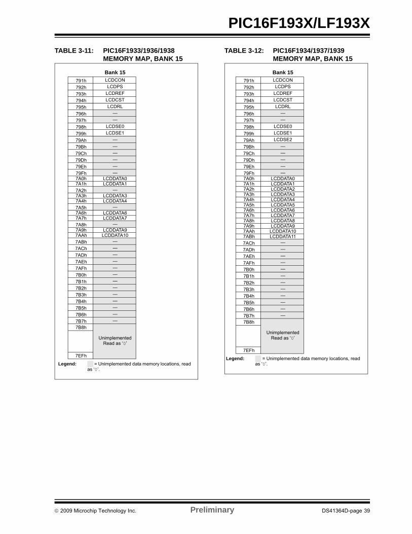
PIC16F193X/LF193X
TABLE 3-11: PIC16F1933/1936/1938 MEMORY MAP, BANK 15
TABLE 3-12: PIC16F1934/1937/1939 MEMORY MAP, BANK 15
Legend: = Unimplemented data memory locations, read as ‘0’.
Bank 15
791h LCDCON
792h LCDPS
793h LCDREF
794h LCDCST
795h LCDRL
796h —
797h —
798h LCDSE0
799h LCDSE1
79Ah —
79Bh —
79Ch —
79Dh —
79Eh —
79Fh —7A0h LCDDATA07A1h LCDDATA1
7A2h —7A3h LCDDATA37A4h LCDDATA4
7A5h —7A6h LCDDATA67A7h LCDDATA7
7A8h —7A9h LCDDATA97AAh LCDDATA10
7ABh —
7ACh —
7ADh —
7AEh —
7AFh —
7B0h —
7B1h —
7B2h —
7B3h —
7B4h —
7B5h —
7B6h —
7B7h —
7B8h
UnimplementedRead as ‘0’
7EFh
Legend: = Unimplemented data memory locations, read as ‘0’.
Bank 15
791h LCDCON
792h LCDPS
793h LCDREF
794h LCDCST
795h LCDRL
796h —
797h —
798h LCDSE0
799h LCDSE1
79Ah LCDSE2
79Bh —
79Ch —
79Dh —
79Eh —
79Fh —7A0h LCDDATA07A1h LCDDATA17A2h LCDDATA27A3h LCDDATA37A4h LCDDATA47A5h LCDDATA57A6h LCDDATA67A7h LCDDATA77A8h LCDDATA87A9h LCDDATA97AAh LCDDATA107ABh LCDDATA11
7ACh —
7ADh —
7AEh —
7AFh —
7B0h —
7B1h —
7B2h —
7B3h —
7B4h —
7B5h —
7B6h —
7B7h —
7B8h
UnimplementedRead as ‘0’
7EFh
2009 Microchip Technology Inc. Preliminary DS41364D-page 39
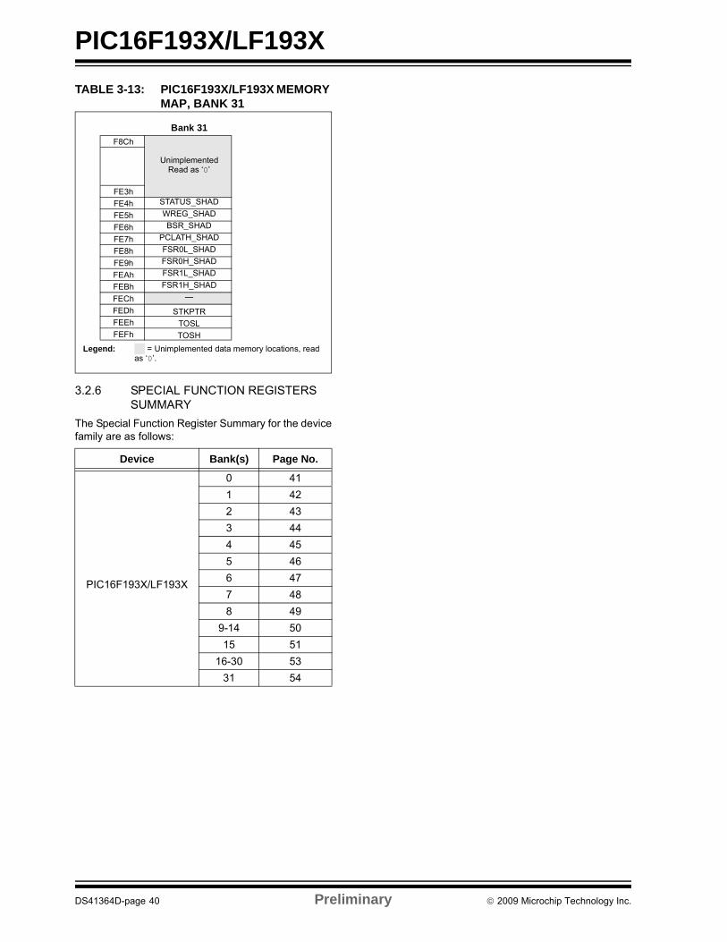
PIC16F193X/LF193X
TABLE 3-13: PIC16F193X/LF193X MEMORY MAP, BANK 31
3.2.6 SPECIAL FUNCTION REGISTERS SUMMARY
The Special Function Register Summary for the devicefamily are as follows:
Device Bank(s) Page No.
PIC16F193X/LF193X
0 41
1 42
2 43
3 44
4 45
5 46
6 47
7 48
8 49
9-14 50
15 51
16-30 53
31 54
Legend: = Unimplemented data memory locations, read as ‘0’.
Bank 31
F8Ch
UnimplementedRead as ‘0’
FE3h
FE4h STATUS_SHAD
FE5h WREG_SHAD
FE6h BSR_SHAD
FE7h PCLATH_SHAD
FE8h FSR0L_SHAD
FE9h FSR0H_SHAD
FEAh FSR1L_SHAD
FEBh FSR1H_SHAD
FECh —
FEDh STKPTRFEEh TOSLFEFh TOSH
DS41364D-page 40 Preliminary 2009 Microchip Technology Inc.
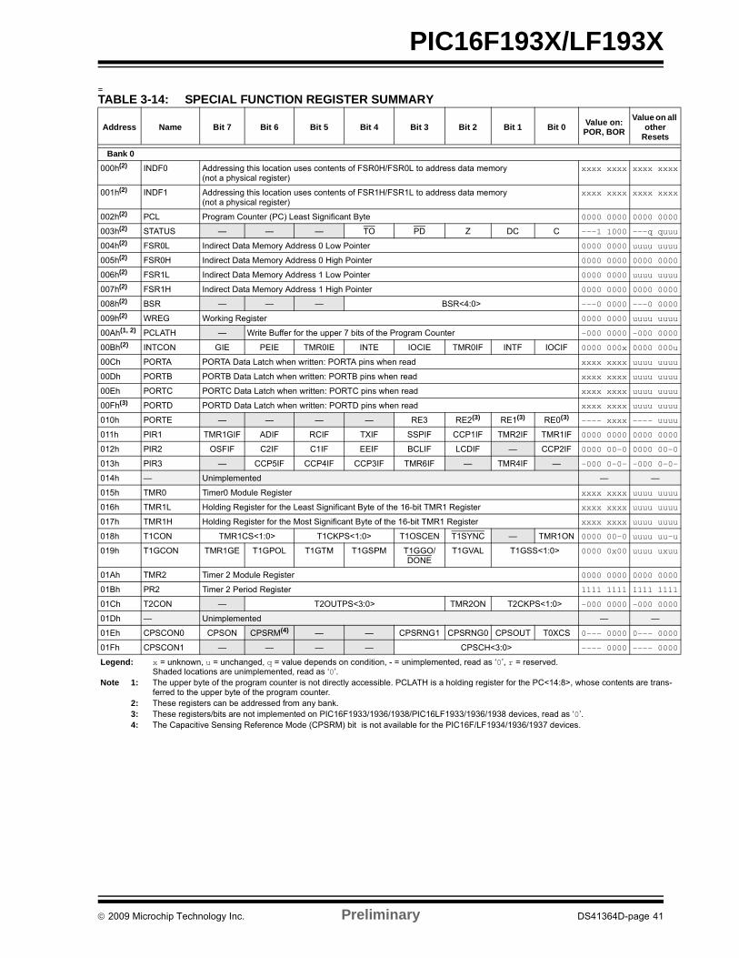
PIC16F193X/LF193X
=TABLE 3-14: SPECIAL FUNCTION REGISTER SUMMARY
Address Name Bit 7 Bit 6 Bit 5 Bit 4 Bit 3 Bit 2 Bit 1 Bit 0Value on:POR, BOR
Value on allother
Resets
Bank 0
000h(2) INDF0 Addressing this location uses contents of FSR0H/FSR0L to address data memory(not a physical register)
xxxx xxxx xxxx xxxx
001h(2) INDF1 Addressing this location uses contents of FSR1H/FSR1L to address data memory(not a physical register)
xxxx xxxx xxxx xxxx
002h(2) PCL Program Counter (PC) Least Significant Byte 0000 0000 0000 0000
003h(2) STATUS — — — TO PD Z DC C ---1 1000 ---q quuu
004h(2) FSR0L Indirect Data Memory Address 0 Low Pointer 0000 0000 uuuu uuuu
005h(2) FSR0H Indirect Data Memory Address 0 High Pointer 0000 0000 0000 0000
006h(2) FSR1L Indirect Data Memory Address 1 Low Pointer 0000 0000 uuuu uuuu
007h(2) FSR1H Indirect Data Memory Address 1 High Pointer 0000 0000 0000 0000
008h(2) BSR — — — BSR<4:0> ---0 0000 ---0 0000
009h(2) WREG Working Register 0000 0000 uuuu uuuu
00Ah(1, 2) PCLATH — Write Buffer for the upper 7 bits of the Program Counter -000 0000 -000 0000
00Bh(2) INTCON GIE PEIE TMR0IE INTE IOCIE TMR0IF INTF IOCIF 0000 000x 0000 000u
00Ch PORTA PORTA Data Latch when written: PORTA pins when read xxxx xxxx uuuu uuuu
00Dh PORTB PORTB Data Latch when written: PORTB pins when read xxxx xxxx uuuu uuuu
00Eh PORTC PORTC Data Latch when written: PORTC pins when read xxxx xxxx uuuu uuuu
00Fh(3) PORTD PORTD Data Latch when written: PORTD pins when read xxxx xxxx uuuu uuuu
010h PORTE — — — — RE3 RE2(3) RE1(3) RE0(3) ---- xxxx ---- uuuu
011h PIR1 TMR1GIF ADIF RCIF TXIF SSPIF CCP1IF TMR2IF TMR1IF 0000 0000 0000 0000
012h PIR2 OSFIF C2IF C1IF EEIF BCLIF LCDIF — CCP2IF 0000 00-0 0000 00-0
013h PIR3 — CCP5IF CCP4IF CCP3IF TMR6IF — TMR4IF — -000 0-0- -000 0-0-
014h — Unimplemented — —
015h TMR0 Timer0 Module Register xxxx xxxx uuuu uuuu
016h TMR1L Holding Register for the Least Significant Byte of the 16-bit TMR1 Register xxxx xxxx uuuu uuuu
017h TMR1H Holding Register for the Most Significant Byte of the 16-bit TMR1 Register xxxx xxxx uuuu uuuu
018h T1CON TMR1CS<1:0> T1CKPS<1:0> T1OSCEN T1SYNC — TMR1ON 0000 00-0 uuuu uu-u
019h T1GCON TMR1GE T1GPOL T1GTM T1GSPM T1GGO/DONE
T1GVAL T1GSS<1:0> 0000 0x00 uuuu uxuu
01Ah TMR2 Timer 2 Module Register 0000 0000 0000 0000
01Bh PR2 Timer 2 Period Register 1111 1111 1111 1111
01Ch T2CON — T2OUTPS<3:0> TMR2ON T2CKPS<1:0> -000 0000 -000 0000
01Dh — Unimplemented — —
01Eh CPSCON0 CPSON CPSRM(4) — — CPSRNG1 CPSRNG0 CPSOUT T0XCS 0--- 0000 0--- 0000
01Fh CPSCON1 — — — — CPSCH<3:0> ---- 0000 ---- 0000
Legend: x = unknown, u = unchanged, q = value depends on condition, - = unimplemented, read as ‘0’, r = reserved. Shaded locations are unimplemented, read as ‘0’.
Note 1: The upper byte of the program counter is not directly accessible. PCLATH is a holding register for the PC<14:8>, whose contents are trans-ferred to the upper byte of the program counter.
2: These registers can be addressed from any bank.3: These registers/bits are not implemented on PIC16F1933/1936/1938/PIC16LF1933/1936/1938 devices, read as ‘0’.4: The Capacitive Sensing Reference Mode (CPSRM) bit is not available for the PIC16F/LF1934/1936/1937 devices.
2009 Microchip Technology Inc. Preliminary DS41364D-page 41

PIC16F193X/LF193X
Bank 1
080h(2) INDF0 Addressing this location uses contents of FSR0H/FSR0L to address data memory(not a physical register)
xxxx xxxx xxxx xxxx
081h(2) INDF1 Addressing this location uses contents of FSR1H/FSR1L to address data memory(not a physical register)
xxxx xxxx xxxx xxxx
082h(2) PCL Program Counter (PC) Least Significant Byte 0000 0000 0000 0000
083h(2) STATUS — — — TO PD Z DC C ---1 1000 ---q quuu
084h(2) FSR0L Indirect Data Memory Address 0 Low Pointer 0000 0000 uuuu uuuu
085h(2) FSR0H Indirect Data Memory Address 0 High Pointer 0000 0000 0000 0000
086h(2) FSR1L Indirect Data Memory Address 1 Low Pointer 0000 0000 uuuu uuuu
087h(2) FSR1H Indirect Data Memory Address 1 High Pointer 0000 0000 0000 0000
088h(2) BSR — — — BSR<4:0> ---0 0000 ---0 0000
089h(2) WREG Working Register 0000 0000 uuuu uuuu
08Ah(1, 2) PCLATH — Write Buffer for the upper 7 bits of the Program Counter -000 0000 -000 0000
08Bh(2) INTCON GIE PEIE TMR0IE INTE IOCIE TMR0IF INTF IOCIF 0000 000x 0000 000u
08Ch TRISA PORTA Data Direction Register 1111 1111 1111 1111
08Dh TRISB PORTB Data Direction Register 1111 1111 1111 1111
08Eh TRISC PORTC Data Direction Register 1111 1111 1111 1111
08Fh(3) TRISD PORTD Data Direction Register 1111 1111 1111 1111
090h TRISE — — — — TRISE3 TRISE2(3) TRISE1(3) TRISE0(3) ---- 1111 ---- 1111
091h PIE1 TMR1GIE ADIE RCIE TXIE SSPIE CCP1IE TMR2IE TMR1IE 0000 0000 0000 0000
092h PIE2 OSFIE C2IE C1IE EEIE BCLIE LCDIE — CCP2IE 0000 00-0 0000 00-0
093h PIE3 — CCP5IE CCP4IE CCP3IE TMR6IE — TMR4IE — -000 0-0- -000 0-0-
094h — Unimplemented — —
095h OPTION_REG WPUEN INTEDG TMROCS TMROSE PSA PS<2:0> 1111 1111 1111 1111
096h PCON STKOVF STKUNF — — RMCLR RI POR BOR 00-- 11qq qq-- qquu
097h WDTCON — — WDTPS<4:0> SWDTEN --01 0110 --01 0110
098h OSCTUNE — — TUN<5:0> --00 0000 --00 0000
099h OSCCON SPLLEN IRCF<3:0> — SCS<1:0> 0011 1-00 0011 1-00
09Ah OSCSTAT T1OSCR PLLR OSTS HFIOFR HFIOFL MFIOFR LFIOFR HFIOFS 00q0 0q0- qqqq qq0-
09Bh ADRESL A/D Result Register Low xxxx xxxx uuuu uuuu
09Ch ADRESH A/D Result Register High xxxx xxxx uuuu uuuu
09Dh ADCON0 — CHS<4:0> GO/DONE ADON -000 0000 -000 0000
09Eh ADCON1 ADFM ADCS<2:0> — ADNREF ADPREF1 ADPREF0 0000 -000 0000 -000
09Fh — Unimplemented — —
TABLE 3-14: SPECIAL FUNCTION REGISTER SUMMARY (CONTINUED)
Address Name Bit 7 Bit 6 Bit 5 Bit 4 Bit 3 Bit 2 Bit 1 Bit 0Value on:POR, BOR
Value on allother
Resets
Legend: x = unknown, u = unchanged, q = value depends on condition, - = unimplemented, read as ‘0’, r = reserved. Shaded locations are unimplemented, read as ‘0’.
Note 1: The upper byte of the program counter is not directly accessible. PCLATH is a holding register for the PC<14:8>, whose contents are trans-ferred to the upper byte of the program counter.
2: These registers can be addressed from any bank.3: These registers/bits are not implemented on PIC16F1933/1936/1938/PIC16LF1933/1936/1938 devices, read as ‘0’.4: The Capacitive Sensing Reference Mode (CPSRM) bit is not available for the PIC16F/LF1934/1936/1937 devices.
DS41364D-page 42 Preliminary 2009 Microchip Technology Inc.

PIC16F193X/LF193X
Bank 2
100h(2) INDF0 Addressing this location uses contents of FSR0H/FSR0L to address data memory(not a physical register)
xxxx xxxx xxxx xxxx
101h(2) INDF1 Addressing this location uses contents of FSR1H/FSR1L to address data memory(not a physical register)
xxxx xxxx xxxx xxxx
102h(2) PCL Program Counter (PC) Least Significant Byte 0000 0000 0000 0000
103h(2) STATUS — — — TO PD Z DC C ---1 1000 ---q quuu
104h(2) FSR0L Indirect Data Memory Address 0 Low Pointer 0000 0000 uuuu uuuu
105h(2) FSR0H Indirect Data Memory Address 0 High Pointer 0000 0000 0000 0000
106h(2) FSR1L Indirect Data Memory Address 1 Low Pointer 0000 0000 uuuu uuuu
107h(2) FSR1H Indirect Data Memory Address 1 High Pointer 0000 0000 0000 0000
108h(2) BSR — — — BSR<4:0> ---0 0000 ---0 0000
109h(2) WREG Working Register 0000 0000 uuuu uuuu
10Ah(1, 2) PCLATH — Write Buffer for the upper 7 bits of the Program Counter -000 0000 -000 0000
10Bh(2) INTCON GIE PEIE TMR0IE INTE IOCIE TMR0IF INTF IOCIF 0000 000x 0000 000u
10Ch LATA PORTA Data Latch xxxx xxxx uuuu uuuu
10Dh LATB PORTB Data Latch xxxx xxxx uuuu uuuu
10Eh LATC PORTC Data Latch xxxx xxxx uuuu uuuu
10Fh(3) LATD PORTD Data Latch xxxx xxxx uuuu uuuu
110h LATE — — — — LATE3 LATE2(3) LATE1(3) LATE0(3) ---- -xxx ---- -uuu
111h CM1CON0 C1ON C1OUT C1OE C1POL — C1SP C1HYS C1SYNC 0000 -100 0000 -100
112h CM1CON1 C1INTP C1INTN C1PCH1 C1PCH0 — — C1NCH<1:0> 0000 --00 0000 --00
113h CM2CON0 C2ON C2OUT C2OE C2POL — C2SP C2HYS C2SYNC 0000 -100 0000 -100
114h CM2CON1 C2INTP C2INTN C2PCH1 C2PCH0 — — C2NCH<1:0> 0000 --00 0000 --00
115h CMOUT — — — — — — MC2OUT MC1OUT ---- --00 ---- --00
116h BORCON SBOREN — — — — — — BORRDY 1--- ---q u--- ---u
117h FVRCON FVREN FVRRDY Reserved Reserved CDAFVR1 CDAFVR0 ADFVR<1:0> 0q00 0000 0q00 0000
118h DACCON0 DACEN DACLPS DACOE --- DACPSS<1:0> --- DACNSS 000- 00-0 000- 00-0
119h DACCON1 --- --- --- DACR<4:0> ---0 0000 ---0 0000
11Ah SRCON0 SRLEN SRCLK2 SRCLK1 SRCLK0 SRQEN SRNQEN SRPS SRPR 0000 0000 0000 0000
11Bh SRCON1 SRSPE SRSCKE SRSC2E SRSC1E SRRPE SRRCKE SRRC2E SRRC1E 0000 0000 0000 0000
11Ch — Unimplemented — —
11Dh APFCON — CCP3SEL T1GSEL P2BSEL SRNQSEL C2OUTSEL SSSEL CCP2SEL -000 0000 -000 0000
11Eh — Unimplemented — —
11Fh — Unimplemented — —
TABLE 3-14: SPECIAL FUNCTION REGISTER SUMMARY (CONTINUED)
Address Name Bit 7 Bit 6 Bit 5 Bit 4 Bit 3 Bit 2 Bit 1 Bit 0Value on:POR, BOR
Value on allother
Resets
Legend: x = unknown, u = unchanged, q = value depends on condition, - = unimplemented, read as ‘0’, r = reserved. Shaded locations are unimplemented, read as ‘0’.
Note 1: The upper byte of the program counter is not directly accessible. PCLATH is a holding register for the PC<14:8>, whose contents are trans-ferred to the upper byte of the program counter.
2: These registers can be addressed from any bank.3: These registers/bits are not implemented on PIC16F1933/1936/1938/PIC16LF1933/1936/1938 devices, read as ‘0’.4: The Capacitive Sensing Reference Mode (CPSRM) bit is not available for the PIC16F/LF1934/1936/1937 devices.
2009 Microchip Technology Inc. Preliminary DS41364D-page 43
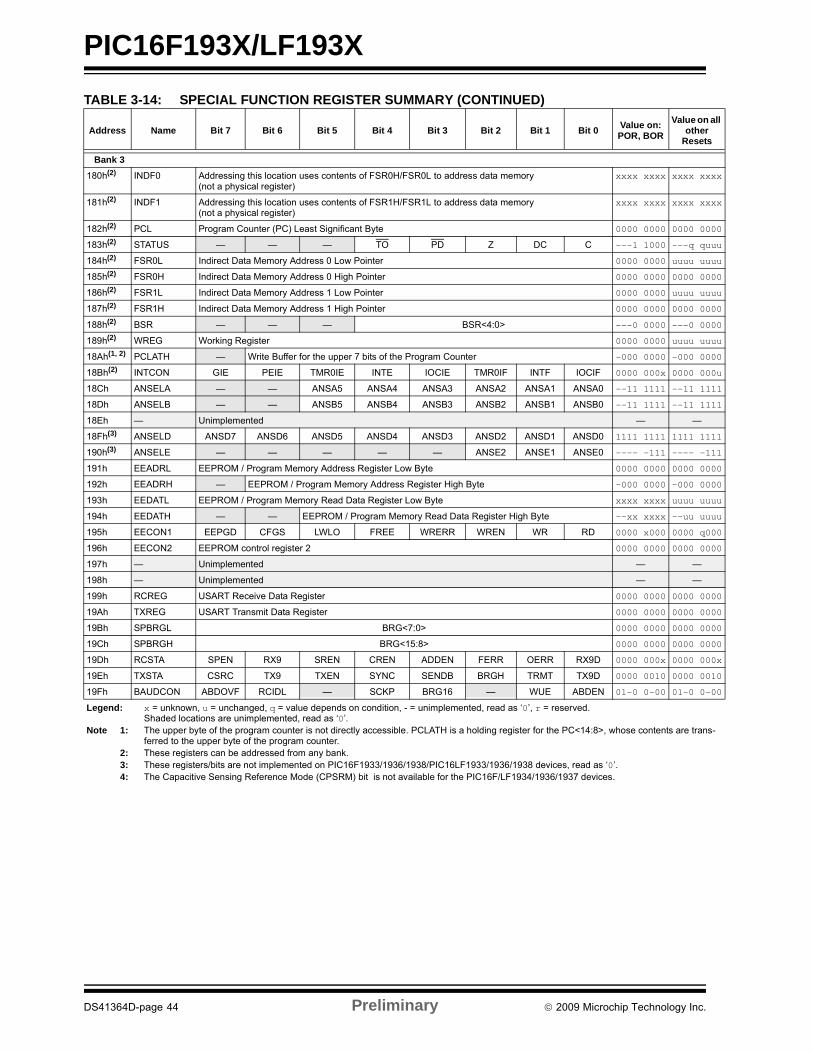
PIC16F193X/LF193X
Bank 3
180h(2) INDF0 Addressing this location uses contents of FSR0H/FSR0L to address data memory(not a physical register)
xxxx xxxx xxxx xxxx
181h(2) INDF1 Addressing this location uses contents of FSR1H/FSR1L to address data memory(not a physical register)
xxxx xxxx xxxx xxxx
182h(2) PCL Program Counter (PC) Least Significant Byte 0000 0000 0000 0000
183h(2) STATUS — — — TO PD Z DC C ---1 1000 ---q quuu
184h(2) FSR0L Indirect Data Memory Address 0 Low Pointer 0000 0000 uuuu uuuu
185h(2) FSR0H Indirect Data Memory Address 0 High Pointer 0000 0000 0000 0000
186h(2) FSR1L Indirect Data Memory Address 1 Low Pointer 0000 0000 uuuu uuuu
187h(2) FSR1H Indirect Data Memory Address 1 High Pointer 0000 0000 0000 0000
188h(2) BSR — — — BSR<4:0> ---0 0000 ---0 0000
189h(2) WREG Working Register 0000 0000 uuuu uuuu
18Ah(1, 2) PCLATH — Write Buffer for the upper 7 bits of the Program Counter -000 0000 -000 0000
18Bh(2) INTCON GIE PEIE TMR0IE INTE IOCIE TMR0IF INTF IOCIF 0000 000x 0000 000u
18Ch ANSELA — — ANSA5 ANSA4 ANSA3 ANSA2 ANSA1 ANSA0 --11 1111 --11 1111
18Dh ANSELB — — ANSB5 ANSB4 ANSB3 ANSB2 ANSB1 ANSB0 --11 1111 --11 1111
18Eh — Unimplemented — —
18Fh(3) ANSELD ANSD7 ANSD6 ANSD5 ANSD4 ANSD3 ANSD2 ANSD1 ANSD0 1111 1111 1111 1111
190h(3) ANSELE — — — — — ANSE2 ANSE1 ANSE0 ---- -111 ---- -111
191h EEADRL EEPROM / Program Memory Address Register Low Byte 0000 0000 0000 0000
192h EEADRH — EEPROM / Program Memory Address Register High Byte -000 0000 -000 0000
193h EEDATL EEPROM / Program Memory Read Data Register Low Byte xxxx xxxx uuuu uuuu
194h EEDATH — — EEPROM / Program Memory Read Data Register High Byte --xx xxxx --uu uuuu
195h EECON1 EEPGD CFGS LWLO FREE WRERR WREN WR RD 0000 x000 0000 q000
196h EECON2 EEPROM control register 2 0000 0000 0000 0000
197h — Unimplemented — —
198h — Unimplemented — —
199h RCREG USART Receive Data Register 0000 0000 0000 0000
19Ah TXREG USART Transmit Data Register 0000 0000 0000 0000
19Bh SPBRGL BRG<7:0> 0000 0000 0000 0000
19Ch SPBRGH BRG<15:8> 0000 0000 0000 0000
19Dh RCSTA SPEN RX9 SREN CREN ADDEN FERR OERR RX9D 0000 000x 0000 000x
19Eh TXSTA CSRC TX9 TXEN SYNC SENDB BRGH TRMT TX9D 0000 0010 0000 0010
19Fh BAUDCON ABDOVF RCIDL — SCKP BRG16 — WUE ABDEN 01-0 0-00 01-0 0-00
TABLE 3-14: SPECIAL FUNCTION REGISTER SUMMARY (CONTINUED)
Address Name Bit 7 Bit 6 Bit 5 Bit 4 Bit 3 Bit 2 Bit 1 Bit 0Value on:POR, BOR
Value on allother
Resets
Legend: x = unknown, u = unchanged, q = value depends on condition, - = unimplemented, read as ‘0’, r = reserved. Shaded locations are unimplemented, read as ‘0’.
Note 1: The upper byte of the program counter is not directly accessible. PCLATH is a holding register for the PC<14:8>, whose contents are trans-ferred to the upper byte of the program counter.
2: These registers can be addressed from any bank.3: These registers/bits are not implemented on PIC16F1933/1936/1938/PIC16LF1933/1936/1938 devices, read as ‘0’.4: The Capacitive Sensing Reference Mode (CPSRM) bit is not available for the PIC16F/LF1934/1936/1937 devices.
DS41364D-page 44 Preliminary 2009 Microchip Technology Inc.

PIC16F193X/LF193X
Bank 4
200h(2) INDF0 Addressing this location uses contents of FSR0H/FSR0L to address data memory(not a physical register)
xxxx xxxx xxxx xxxx
201h(2) INDF1 Addressing this location uses contents of FSR1H/FSR1L to address data memory(not a physical register)
xxxx xxxx xxxx xxxx
202h(2) PCL Program Counter (PC) Least Significant Byte 0000 0000 0000 0000
203h(2) STATUS — — — TO PD Z DC C ---1 1000 ---q quuu
204h(2) FSR0L Indirect Data Memory Address 0 Low Pointer 0000 0000 uuuu uuuu
205h(2) FSR0H Indirect Data Memory Address 0 High Pointer 0000 0000 0000 0000
206h(2) FSR1L Indirect Data Memory Address 1 Low Pointer 0000 0000 uuuu uuuu
207h(2) FSR1H Indirect Data Memory Address 1 High Pointer 0000 0000 0000 0000
208h(2) BSR — — — BSR<4:0> ---0 0000 ---0 0000
209h(2) WREG Working Register 0000 0000 uuuu uuuu
20Ah(1, 2) PCLATH — Write Buffer for the upper 7 bits of the Program Counter -000 0000 -000 0000
20Bh(2) INTCON GIE PEIE TMR0IE INTE IOCIE TMR0IF INTF IOCIF 0000 000x 0000 000u
20Ch — Unimplemented — —
20Dh WPUB WPUB7 WPUB6 WPUB5 WPUB4 WPUB3 WPUB2 WPUB1 WPUB0 1111 1111 1111 1111
20Eh — Unimplemented — —
20Fh — Unimplemented — —
210h WPUE — — — — WPUE3 — — — ---- 1--- ---- 1---
211h SSPBUF Synchronous Serial Port Receive Buffer/Transmit Register xxxx xxxx uuuu uuuu
212h SSPADD ADD<7:0> 0000 0000 0000 0000
213h SSPMSK MSK<7:0> 1111 1111 1111 1111
214h SSPSTAT SMP CKE D/A P S R/W UA BF 0000 0000 0000 0000
215h SSPCON1 WCOL SSPOV SSPEN CKP SSPM<3:0> 0000 0000 0000 0000
216h SSPCON2 GCEN ACKSTAT ACKDT ACKEN RCEN PEN RSEN SEN 0000 0000 0000 0000
217h SSPCON3 ACKTIM PCIE SCIE BOEN SDAHT SBCDE AHEN DHEN 0000 0000 0000 0000
218h — Unimplemented — —
219h — Unimplemented — —
21Ah — Unimplemented — —
21Bh — Unimplemented — —
21Ch — Unimplemented — —
21Dh — Unimplemented — —
21Eh — Unimplemented — —
21Fh — Unimplemented — —
TABLE 3-14: SPECIAL FUNCTION REGISTER SUMMARY (CONTINUED)
Address Name Bit 7 Bit 6 Bit 5 Bit 4 Bit 3 Bit 2 Bit 1 Bit 0Value on:POR, BOR
Value on allother
Resets
Legend: x = unknown, u = unchanged, q = value depends on condition, - = unimplemented, read as ‘0’, r = reserved. Shaded locations are unimplemented, read as ‘0’.
Note 1: The upper byte of the program counter is not directly accessible. PCLATH is a holding register for the PC<14:8>, whose contents are trans-ferred to the upper byte of the program counter.
2: These registers can be addressed from any bank.3: These registers/bits are not implemented on PIC16F1933/1936/1938/PIC16LF1933/1936/1938 devices, read as ‘0’.4: The Capacitive Sensing Reference Mode (CPSRM) bit is not available for the PIC16F/LF1934/1936/1937 devices.
2009 Microchip Technology Inc. Preliminary DS41364D-page 45

PIC16F193X/LF193X
Bank 5
280h(2) INDF0 Addressing this location uses contents of FSR0H/FSR0L to address data memory(not a physical register)
xxxx xxxx xxxx xxxx
281h(2) INDF1 Addressing this location uses contents of FSR1H/FSR1L to address data memory(not a physical register)
xxxx xxxx xxxx xxxx
282h(2) PCL Program Counter (PC) Least Significant Byte 0000 0000 0000 0000
283h(2) STATUS — — — TO PD Z DC C ---1 1000 ---q quuu
284h(2) FSR0L Indirect Data Memory Address 0 Low Pointer 0000 0000 uuuu uuuu
285h(2) FSR0H Indirect Data Memory Address 0 High Pointer 0000 0000 0000 0000
286h(2) FSR1L Indirect Data Memory Address 1 Low Pointer 0000 0000 uuuu uuuu
287h(2) FSR1H Indirect Data Memory Address 1 High Pointer 0000 0000 0000 0000
288h(2) BSR — — — BSR<4:0> ---0 0000 ---0 0000
289h(2) WREG Working Register 0000 0000 uuuu uuuu
28Ah(1, 2) PCLATH — Write Buffer for the upper 7 bits of the Program Counter -000 0000 -000 0000
28Bh(2) INTCON GIE PEIE TMR0IE INTE IOCIE TMR0IF INTF IOCIF 0000 000x 0000 000u
28Ch — Unimplemented — —
28Dh — Unimplemented — —
28Eh — Unimplemented — —
28Fh — Unimplemented — —
290h — Unimplemented — —
291h CCPR1L Capture/Compare/PWM Register 1 (LSB) xxxx xxxx uuuu uuuu
292h CCPR1H Capture/Compare/PWM Register 1 (MSB) xxxx xxxx uuuu uuuu
293h CCP1CON P1M<1:0> DC1B<1:0> CCP1M<3:0> 0000 0000 0000 0000
294h PWM1CON P1RSEN P1DC<6:0> 0000 0000 0000 0000
295h CCP1AS CCP1ASE CCP1AS<2:0> PSS1AC<1:0> PSS1BD<1:0> 0000 0000 0000 0000
296h PSTR1CON — — — STR1SYNC STR1D STR1C STR1B STR1A ---0 0001 ---0 0001
297h — Unimplemented — —
298h CCPR2L Capture/Compare/PWM Register 2 (LSB) xxxx xxxx uuuu uuuu
299h CCPR2H Capture/Compare/PWM Register 2 (MSB) xxxx xxxx uuuu uuuu
29Ah CCP2CON P2M<1:0> DC2B<1:0> CCP2M<3:0> 0000 0000 0000 0000
29Bh PWM2CON P2RSEN P2DC<6:0> 0000 0000 0000 0000
29Ch CCP2AS CCP2ASE CCP2AS<2:0> PSS2AC<1:0> PSS2BD<1:0> 0000 0000 0000 0000
29Dh PSTR2CON — — — STR2SYNC STR2D STR2C STR2B STR2A ---0 0001 ---0 0001
29Eh CCPTMRS0 C4TSEL1 C4TSEL0 C3TSEL1 C3TSEL0 C2TSEL1 C2TSEL0 C1TSEL1 C1TSEL0 0000 0000 0000 0000
29Fh CCPTMRS1 — — — — — — C5TSEL<1:0> ---- --00 ---- --00
TABLE 3-14: SPECIAL FUNCTION REGISTER SUMMARY (CONTINUED)
Address Name Bit 7 Bit 6 Bit 5 Bit 4 Bit 3 Bit 2 Bit 1 Bit 0Value on:POR, BOR
Value on allother
Resets
Legend: x = unknown, u = unchanged, q = value depends on condition, - = unimplemented, read as ‘0’, r = reserved. Shaded locations are unimplemented, read as ‘0’.
Note 1: The upper byte of the program counter is not directly accessible. PCLATH is a holding register for the PC<14:8>, whose contents are trans-ferred to the upper byte of the program counter.
2: These registers can be addressed from any bank.3: These registers/bits are not implemented on PIC16F1933/1936/1938/PIC16LF1933/1936/1938 devices, read as ‘0’.4: The Capacitive Sensing Reference Mode (CPSRM) bit is not available for the PIC16F/LF1934/1936/1937 devices.
DS41364D-page 46 Preliminary 2009 Microchip Technology Inc.
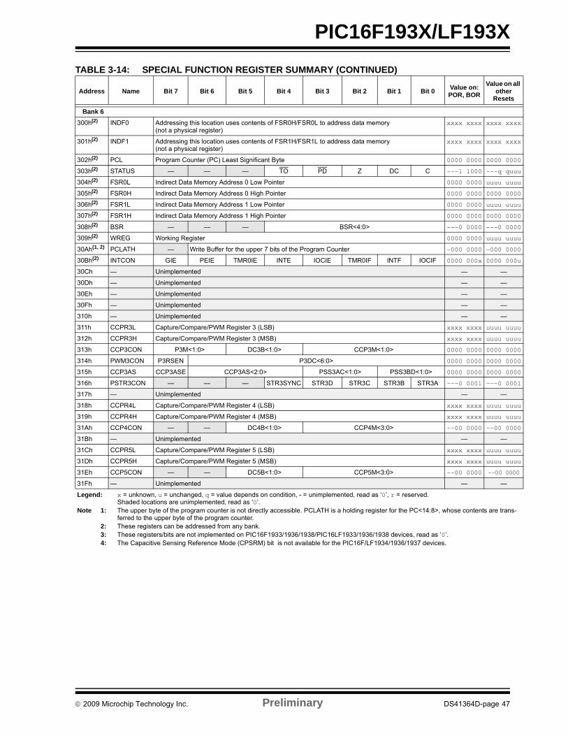
PIC16F193X/LF193X
Bank 6
300h(2) INDF0 Addressing this location uses contents of FSR0H/FSR0L to address data memory(not a physical register)
xxxx xxxx xxxx xxxx
301h(2) INDF1 Addressing this location uses contents of FSR1H/FSR1L to address data memory(not a physical register)
xxxx xxxx xxxx xxxx
302h(2) PCL Program Counter (PC) Least Significant Byte 0000 0000 0000 0000
303h(2) STATUS — — — TO PD Z DC C ---1 1000 ---q quuu
304h(2) FSR0L Indirect Data Memory Address 0 Low Pointer 0000 0000 uuuu uuuu
305h(2) FSR0H Indirect Data Memory Address 0 High Pointer 0000 0000 0000 0000
306h(2) FSR1L Indirect Data Memory Address 1 Low Pointer 0000 0000 uuuu uuuu
307h(2) FSR1H Indirect Data Memory Address 1 High Pointer 0000 0000 0000 0000
308h(2) BSR — — — BSR<4:0> ---0 0000 ---0 0000
309h(2) WREG Working Register 0000 0000 uuuu uuuu
30Ah(1, 2) PCLATH — Write Buffer for the upper 7 bits of the Program Counter -000 0000 -000 0000
30Bh(2) INTCON GIE PEIE TMR0IE INTE IOCIE TMR0IF INTF IOCIF 0000 000x 0000 000u
30Ch — Unimplemented — —
30Dh — Unimplemented — —
30Eh — Unimplemented — —
30Fh — Unimplemented — —
310h — Unimplemented — —
311h CCPR3L Capture/Compare/PWM Register 3 (LSB) xxxx xxxx uuuu uuuu
312h CCPR3H Capture/Compare/PWM Register 3 (MSB) xxxx xxxx uuuu uuuu
313h CCP3CON P3M<1:0> DC3B<1:0> CCP3M<1:0> 0000 0000 0000 0000
314h PWM3CON P3RSEN P3DC<6:0> 0000 0000 0000 0000
315h CCP3AS CCP3ASE CCP3AS<2:0> PSS3AC<1:0> PSS3BD<1:0> 0000 0000 0000 0000
316h PSTR3CON — — — STR3SYNC STR3D STR3C STR3B STR3A ---0 0001 ---0 0001
317h — Unimplemented — —
318h CCPR4L Capture/Compare/PWM Register 4 (LSB) xxxx xxxx uuuu uuuu
319h CCPR4H Capture/Compare/PWM Register 4 (MSB) xxxx xxxx uuuu uuuu
31Ah CCP4CON — — DC4B<1:0> CCP4M<3:0> --00 0000 --00 0000
31Bh — Unimplemented — —
31Ch CCPR5L Capture/Compare/PWM Register 5 (LSB) xxxx xxxx uuuu uuuu
31Dh CCPR5H Capture/Compare/PWM Register 5 (MSB) xxxx xxxx uuuu uuuu
31Eh CCP5CON — — DC5B<1:0> CCP5M<3:0> --00 0000 --00 0000
31Fh — Unimplemented — —
TABLE 3-14: SPECIAL FUNCTION REGISTER SUMMARY (CONTINUED)
Address Name Bit 7 Bit 6 Bit 5 Bit 4 Bit 3 Bit 2 Bit 1 Bit 0Value on:POR, BOR
Value on allother
Resets
Legend: x = unknown, u = unchanged, q = value depends on condition, - = unimplemented, read as ‘0’, r = reserved. Shaded locations are unimplemented, read as ‘0’.
Note 1: The upper byte of the program counter is not directly accessible. PCLATH is a holding register for the PC<14:8>, whose contents are trans-ferred to the upper byte of the program counter.
2: These registers can be addressed from any bank.3: These registers/bits are not implemented on PIC16F1933/1936/1938/PIC16LF1933/1936/1938 devices, read as ‘0’.4: The Capacitive Sensing Reference Mode (CPSRM) bit is not available for the PIC16F/LF1934/1936/1937 devices.
2009 Microchip Technology Inc. Preliminary DS41364D-page 47
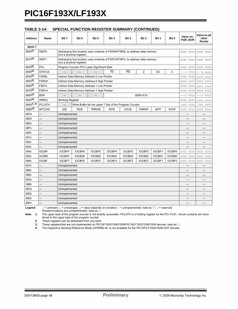
PIC16F193X/LF193X
Bank 7
380h(2) INDF0 Addressing this location uses contents of FSR0H/FSR0L to address data memory(not a physical register)
xxxx xxxx xxxx xxxx
381h(2) INDF1 Addressing this location uses contents of FSR1H/FSR1L to address data memory(not a physical register)
xxxx xxxx xxxx xxxx
382h(2) PCL Program Counter (PC) Least Significant Byte 0000 0000 0000 0000
383h(2) STATUS — — — TO PD Z DC C ---1 1000 ---q quuu
384h(2) FSR0L Indirect Data Memory Address 0 Low Pointer 0000 0000 uuuu uuuu
385h(2) FSR0H Indirect Data Memory Address 0 High Pointer 0000 0000 0000 0000
386h(2) FSR1L Indirect Data Memory Address 1 Low Pointer 0000 0000 uuuu uuuu
387h(2) FSR1H Indirect Data Memory Address 1 High Pointer 0000 0000 0000 0000
388h(2) BSR — — — BSR<4:0> ---0 0000 ---0 0000
389h(2) WREG Working Register 0000 0000 uuuu uuuu
38Ah(1, 2) PCLATH — Write Buffer for the upper 7 bits of the Program Counter -000 0000 -000 0000
38Bh(2) INTCON GIE PEIE TMR0IE INTE IOCIE TMR0IF INTF IOCIF 0000 000x 0000 000u
38Ch — Unimplemented — —
38Dh — Unimplemented — —
38Eh — Unimplemented — —
38Fh — Unimplemented — —
390h — Unimplemented — —
391h — Unimplemented — —
392h — Unimplemented — —
393h — Unimplemented — —
394h IOCBP IOCBP7 IOCBP6 IOCBP5 IOCBP4 IOCBP3 IOCBP2 IOCBP1 IOCBP0 0000 0000 0000 0000
395h IOCBN IOCBN7 IOCBN6 IOCBN5 IOCBN4 IOCBN3 IOCBN2 IOCBN1 IOCBN0 0000 0000 0000 0000
396h IOCBF IOCBF7 IOCBF6 IOCBF5 IOCBF4 IOCBF3 IOCBF2 IOCBF1 IOCBF0 0000 0000 0000 0000
397h — Unimplemented — —
398h — Unimplemented — —
399h — Unimplemented — —
39Ah — Unimplemented — —
39Bh — Unimplemented — —
39Ch — Unimplemented — —
39Dh — Unimplemented — —
39Eh — Unimplemented — —
39Fh — Unimplemented — —
TABLE 3-14: SPECIAL FUNCTION REGISTER SUMMARY (CONTINUED)
Address Name Bit 7 Bit 6 Bit 5 Bit 4 Bit 3 Bit 2 Bit 1 Bit 0Value on:POR, BOR
Value on allother
Resets
Legend: x = unknown, u = unchanged, q = value depends on condition, - = unimplemented, read as ‘0’, r = reserved. Shaded locations are unimplemented, read as ‘0’.
Note 1: The upper byte of the program counter is not directly accessible. PCLATH is a holding register for the PC<14:8>, whose contents are trans-ferred to the upper byte of the program counter.
2: These registers can be addressed from any bank.3: These registers/bits are not implemented on PIC16F1933/1936/1938/PIC16LF1933/1936/1938 devices, read as ‘0’.4: The Capacitive Sensing Reference Mode (CPSRM) bit is not available for the PIC16F/LF1934/1936/1937 devices.
DS41364D-page 48 Preliminary 2009 Microchip Technology Inc.
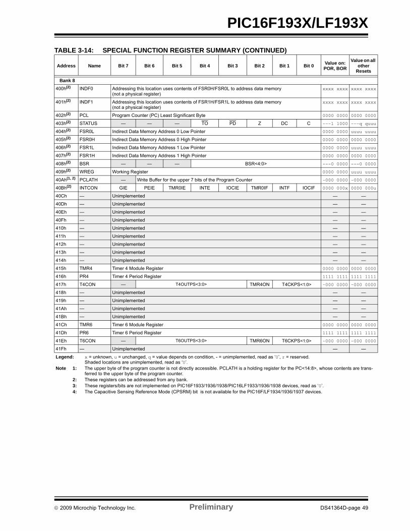
PIC16F193X/LF193X
Bank 8
400h(2) INDF0 Addressing this location uses contents of FSR0H/FSR0L to address data memory(not a physical register)
xxxx xxxx xxxx xxxx
401h(2) INDF1 Addressing this location uses contents of FSR1H/FSR1L to address data memory(not a physical register)
xxxx xxxx xxxx xxxx
402h(2) PCL Program Counter (PC) Least Significant Byte 0000 0000 0000 0000
403h(2) STATUS — — — TO PD Z DC C ---1 1000 ---q quuu
404h(2) FSR0L Indirect Data Memory Address 0 Low Pointer 0000 0000 uuuu uuuu
405h(2) FSR0H Indirect Data Memory Address 0 High Pointer 0000 0000 0000 0000
406h(2) FSR1L Indirect Data Memory Address 1 Low Pointer 0000 0000 uuuu uuuu
407h(2) FSR1H Indirect Data Memory Address 1 High Pointer 0000 0000 0000 0000
408h(2) BSR — — — BSR<4:0> ---0 0000 ---0 0000
409h(2) WREG Working Register 0000 0000 uuuu uuuu
40Ah(1, 2) PCLATH — Write Buffer for the upper 7 bits of the Program Counter -000 0000 -000 0000
40Bh(2) INTCON GIE PEIE TMR0IE INTE IOCIE TMR0IF INTF IOCIF 0000 000x 0000 000u
40Ch — Unimplemented — —
40Dh — Unimplemented — —
40Eh — Unimplemented — —
40Fh — Unimplemented — —
410h — Unimplemented — —
411h — Unimplemented — —
412h — Unimplemented — —
413h — Unimplemented — —
414h — Unimplemented — —
415h TMR4 Timer 4 Module Register 0000 0000 0000 0000
416h PR4 Timer 4 Period Register 1111 1111 1111 1111
417h T4CON — T4OUTPS<3:0> TMR4ON T4CKPS<1:0> -000 0000 -000 0000
418h — Unimplemented — —
419h — Unimplemented — —
41Ah — Unimplemented — —
41Bh — Unimplemented — —
41Ch TMR6 Timer 6 Module Register 0000 0000 0000 0000
41Dh PR6 Timer 6 Period Register 1111 1111 1111 1111
41Eh T6CON — T6OUTPS<3:0> TMR6ON T6CKPS<1:0> -000 0000 -000 0000
41Fh — Unimplemented — —
TABLE 3-14: SPECIAL FUNCTION REGISTER SUMMARY (CONTINUED)
Address Name Bit 7 Bit 6 Bit 5 Bit 4 Bit 3 Bit 2 Bit 1 Bit 0Value on:POR, BOR
Value on allother
Resets
Legend: x = unknown, u = unchanged, q = value depends on condition, - = unimplemented, read as ‘0’, r = reserved. Shaded locations are unimplemented, read as ‘0’.
Note 1: The upper byte of the program counter is not directly accessible. PCLATH is a holding register for the PC<14:8>, whose contents are trans-ferred to the upper byte of the program counter.
2: These registers can be addressed from any bank.3: These registers/bits are not implemented on PIC16F1933/1936/1938/PIC16LF1933/1936/1938 devices, read as ‘0’.4: The Capacitive Sensing Reference Mode (CPSRM) bit is not available for the PIC16F/LF1934/1936/1937 devices.
2009 Microchip Technology Inc. Preliminary DS41364D-page 49
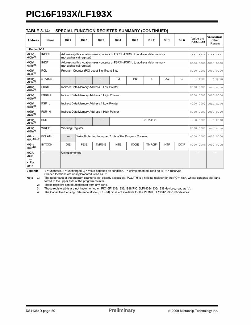
PIC16F193X/LF193X
Banks 9-14
x00h/x80h(2)
INDF0 Addressing this location uses contents of FSR0H/FSR0L to address data memory(not a physical register)
xxxx xxxx xxxx xxxx
x00h/x81h(2)
INDF1 Addressing this location uses contents of FSR1H/FSR1L to address data memory(not a physical register)
xxxx xxxx xxxx xxxx
x02h/x82h(2)
PCL Program Counter (PC) Least Significant Byte 0000 0000 0000 0000
x03h/x83h(2)
STATUS — — — TO PD Z DC C ---1 1000 ---q quuu
x04h/x84h(2)
FSR0L Indirect Data Memory Address 0 Low Pointer 0000 0000 uuuu uuuu
x05h/x85h(2)
FSR0H Indirect Data Memory Address 0 High Pointer 0000 0000 0000 0000
x06h/x86h(2)
FSR1L Indirect Data Memory Address 1 Low Pointer 0000 0000 uuuu uuuu
x07h/x87h(2)
FSR1H Indirect Data Memory Address 1 High Pointer 0000 0000 0000 0000
x08h/x88h(2)
BSR — — — BSR<4:0> ---0 0000 ---0 0000
x09h/x89h(2)
WREG Working Register 0000 0000 uuuu uuuu
x0Ah/x8Ah(1),(2)
PCLATH — Write Buffer for the upper 7 bits of the Program Counter -000 0000 -000 0000
x0Bh/x8Bh(2)
INTCON GIE PEIE TMR0IE INTE IOCIE TMR0IF INTF IOCIF 0000 000x 0000 000u
x0Ch/x8Ch —x1Fh/x9Fh
— Unimplemented — —
TABLE 3-14: SPECIAL FUNCTION REGISTER SUMMARY (CONTINUED)
Address Name Bit 7 Bit 6 Bit 5 Bit 4 Bit 3 Bit 2 Bit 1 Bit 0Value on:POR, BOR
Value on allother
Resets
Legend: x = unknown, u = unchanged, q = value depends on condition, - = unimplemented, read as ‘0’, r = reserved. Shaded locations are unimplemented, read as ‘0’.
Note 1: The upper byte of the program counter is not directly accessible. PCLATH is a holding register for the PC<14:8>, whose contents are trans-ferred to the upper byte of the program counter.
2: These registers can be addressed from any bank.3: These registers/bits are not implemented on PIC16F1933/1936/1938/PIC16LF1933/1936/1938 devices, read as ‘0’.4: The Capacitive Sensing Reference Mode (CPSRM) bit is not available for the PIC16F/LF1934/1936/1937 devices.
DS41364D-page 50 Preliminary 2009 Microchip Technology Inc.

PIC16F193X/LF193X
Bank 15
780h(2) INDF0 Addressing this location uses contents of FSR0H/FSR0L to address data memory(not a physical register)
xxxx xxxx xxxx xxxx
781h(2) INDF1 Addressing this location uses contents of FSR1H/FSR1L to address data memory(not a physical register)
xxxx xxxx xxxx xxxx
782h(2) PCL Program Counter (PC) Least Significant Byte 0000 0000 0000 0000
783h(2) STATUS — — — TO PD Z DC C ---1 1000 ---q quuu
784h(2) FSR0L Indirect Data Memory Address 0 Low Pointer 0000 0000 uuuu uuuu
785h(2) FSR0H Indirect Data Memory Address 0 High Pointer 0000 0000 0000 0000
786h(2) FSR1L Indirect Data Memory Address 1 Low Pointer 0000 0000 uuuu uuuu
787h(2) FSR1H Indirect Data Memory Address 1 High Pointer 0000 0000 0000 0000
788h(2) BSR — — — BSR<4:0> ---0 0000 ---0 0000
789h(2) WREG Working Register 0000 0000 uuuu uuuu
78Ah(1, 2) PCLATH — Write Buffer for the upper 7 bits of the Program Counter -000 0000 -000 0000
78Bh(2) INTCON GIE PEIE TMR0IE INTE IOCIE TMR0IF INTF IOCIF 0000 000x 0000 000u
78Ch — Unimplemented — —
78Dh — Unimplemented — —
78Eh — Unimplemented — —
78Fh — Unimplemented — —
790h — Unimplemented — —
791h LCDCON LCDEN SLPEN WERR — CS<1:0> LMUX<1:0> 000- 0011 000- 0011
792h LCDPS WFT BIASMD LCDA WA LP<3:0> 0000 0000 0000 0000
793h LCDREF LCDIRE LCDIRS LCDIRI — VLCD3PE VLCD2PE VLCD1PE — 000- 000- 000- 000-
794h LCDCST — — — — — LCDCST<2:0> ---- -000 ---- -000
795h LCDRL LRLAP<1:0> LRLBP<1:0> — LRLAT<2:0> 0000 -000 0000 -000
796h — Unimplemented — —
797h — Unimplemented — —
798h LCDSE0 SE<7:0> 0000 0000 uuuu uuuu
799h LCDSE1 SE<15:8> 0000 0000 uuuu uuuu
79Ah LCDSE2(3) SE<23:16> 0000 0000 uuuu uuuu
79Bh — Unimplemented — —
79Ch — Unimplemented — —
79Dh — Unimplemented — —
79Eh — Unimplemented — —
79Fh — Unimplemented — —
7A0h LCDDATA0 SEG7COM0
SEG6COM0
SEG5COM0
SEG4COM0
SEG3COM0
SEG2COM0
SEG1COM0
SEG0COM0
xxxx xxxx uuuu uuuu
7A1h LCDDATA1 SEG15COM0
SEG14COM0
SEG13COM0
SEG12COM0
SEG11COM0
SEG10COM0
SEG9COM0
SEG8COM0
xxxx xxxx uuuu uuuu
7A2h LCDDATA2(3) SEG23COM0
SEG22COM0
SEG21COM0
SEG20COM0
SEG19COM0
SEG18COM0
SEG17COM0
SEG16COM0
xxxx xxxx uuuu uuuu
7A3h LCDDATA3 SEG7COM1
SEG6COM1
SEG5COM1
SEG4COM1
SEG3COM1
SEG2COM1
SEG1COM1
SEG0COM1
xxxx xxxx uuuu uuuu
7A4h LCDDATA4 SEG15COM1
SEG14COM1
SEG13COM1
SEG12COM1
SEG11COM1
SEG10COM1
SEG9COM1
SEG8COM1
xxxx xxxx uuuu uuuu
7A5h LCDDATA5(3) SEG23COM1
SEG22COM1
SEG21COM1
SEG20COM1
SEG19COM1
SEG18COM1
SEG17COM1
SEG16COM1
xxxx xxxx uuuu uuuu
TABLE 3-14: SPECIAL FUNCTION REGISTER SUMMARY (CONTINUED)
Address Name Bit 7 Bit 6 Bit 5 Bit 4 Bit 3 Bit 2 Bit 1 Bit 0Value on:POR, BOR
Value on allother
Resets
Legend: x = unknown, u = unchanged, q = value depends on condition, - = unimplemented, read as ‘0’, r = reserved. Shaded locations are unimplemented, read as ‘0’.
Note 1: The upper byte of the program counter is not directly accessible. PCLATH is a holding register for the PC<14:8>, whose contents are trans-ferred to the upper byte of the program counter.
2: These registers can be addressed from any bank.3: These registers/bits are not implemented on PIC16F1933/1936/1938/PIC16LF1933/1936/1938 devices, read as ‘0’.4: The Capacitive Sensing Reference Mode (CPSRM) bit is not available for the PIC16F/LF1934/1936/1937 devices.
2009 Microchip Technology Inc. Preliminary DS41364D-page 51
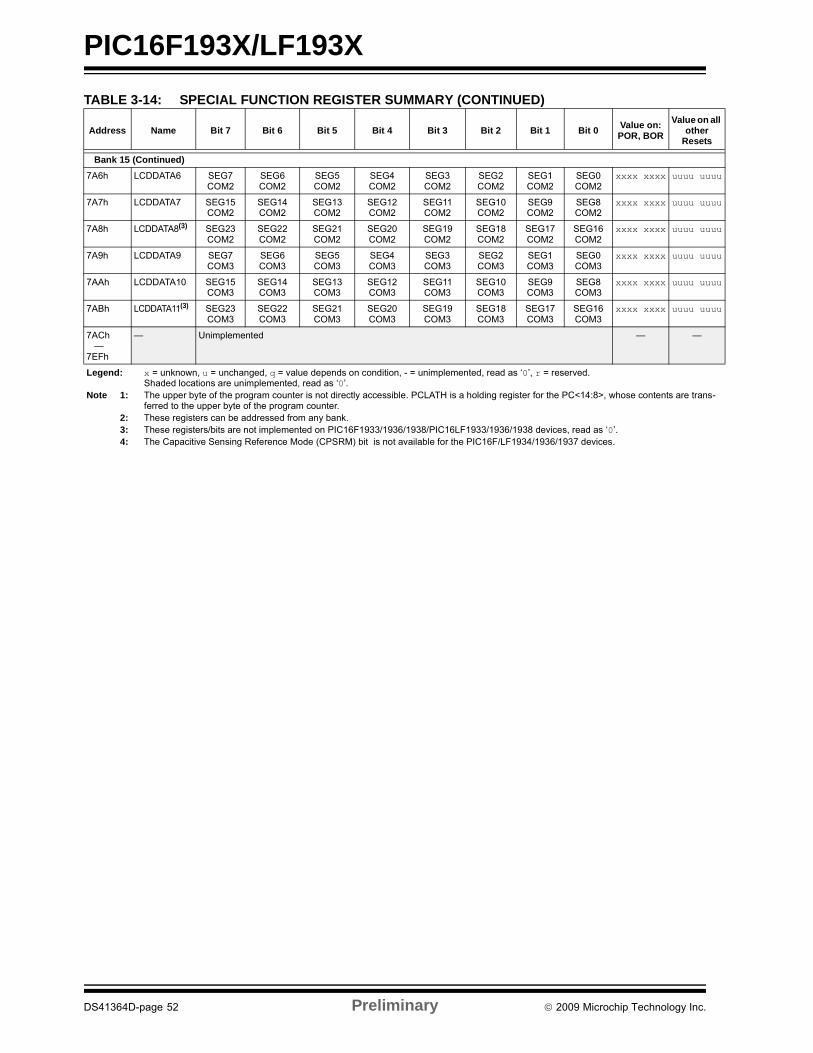
PIC16F193X/LF193X
Bank 15 (Continued)
7A6h LCDDATA6 SEG7COM2
SEG6COM2
SEG5COM2
SEG4COM2
SEG3COM2
SEG2COM2
SEG1COM2
SEG0COM2
xxxx xxxx uuuu uuuu
7A7h LCDDATA7 SEG15COM2
SEG14COM2
SEG13COM2
SEG12COM2
SEG11COM2
SEG10COM2
SEG9COM2
SEG8COM2
xxxx xxxx uuuu uuuu
7A8h LCDDATA8(3) SEG23COM2
SEG22COM2
SEG21COM2
SEG20COM2
SEG19COM2
SEG18COM2
SEG17COM2
SEG16COM2
xxxx xxxx uuuu uuuu
7A9h LCDDATA9 SEG7COM3
SEG6COM3
SEG5COM3
SEG4COM3
SEG3COM3
SEG2COM3
SEG1COM3
SEG0COM3
xxxx xxxx uuuu uuuu
7AAh LCDDATA10 SEG15COM3
SEG14COM3
SEG13COM3
SEG12COM3
SEG11COM3
SEG10COM3
SEG9COM3
SEG8COM3
xxxx xxxx uuuu uuuu
7ABh LCDDATA11(3) SEG23COM3
SEG22COM3
SEG21COM3
SEG20COM3
SEG19COM3
SEG18COM3
SEG17COM3
SEG16COM3
xxxx xxxx uuuu uuuu
7ACh —7EFh
— Unimplemented — —
TABLE 3-14: SPECIAL FUNCTION REGISTER SUMMARY (CONTINUED)
Address Name Bit 7 Bit 6 Bit 5 Bit 4 Bit 3 Bit 2 Bit 1 Bit 0Value on:POR, BOR
Value on allother
Resets
Legend: x = unknown, u = unchanged, q = value depends on condition, - = unimplemented, read as ‘0’, r = reserved. Shaded locations are unimplemented, read as ‘0’.
Note 1: The upper byte of the program counter is not directly accessible. PCLATH is a holding register for the PC<14:8>, whose contents are trans-ferred to the upper byte of the program counter.
2: These registers can be addressed from any bank.3: These registers/bits are not implemented on PIC16F1933/1936/1938/PIC16LF1933/1936/1938 devices, read as ‘0’.4: The Capacitive Sensing Reference Mode (CPSRM) bit is not available for the PIC16F/LF1934/1936/1937 devices.
DS41364D-page 52 Preliminary 2009 Microchip Technology Inc.
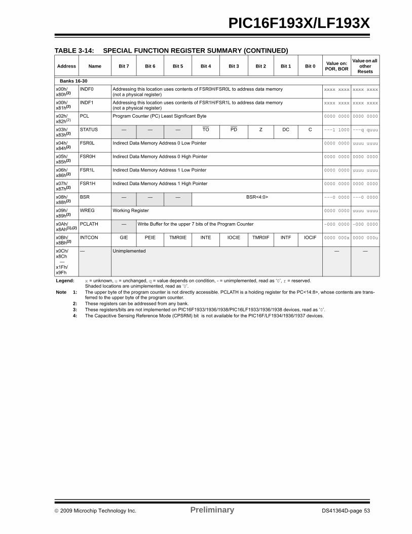
PIC16F193X/LF193X
Banks 16-30
x00h/x80h(2)
INDF0 Addressing this location uses contents of FSR0H/FSR0L to address data memory(not a physical register)
xxxx xxxx xxxx xxxx
x00h/x81h(2)
INDF1 Addressing this location uses contents of FSR1H/FSR1L to address data memory(not a physical register)
xxxx xxxx xxxx xxxx
x02h/x82h(2)
PCL Program Counter (PC) Least Significant Byte 0000 0000 0000 0000
x03h/x83h(2)
STATUS — — — TO PD Z DC C ---1 1000 ---q quuu
x04h/x84h(2)
FSR0L Indirect Data Memory Address 0 Low Pointer 0000 0000 uuuu uuuu
x05h/x85h(2)
FSR0H Indirect Data Memory Address 0 High Pointer 0000 0000 0000 0000
x06h/x86h(2)
FSR1L Indirect Data Memory Address 1 Low Pointer 0000 0000 uuuu uuuu
x07h/x87h(2)
FSR1H Indirect Data Memory Address 1 High Pointer 0000 0000 0000 0000
x08h/x88h(2)
BSR — — — BSR<4:0> ---0 0000 ---0 0000
x09h/x89h(2)
WREG Working Register 0000 0000 uuuu uuuu
x0Ah/x8Ah(1),(2)
PCLATH — Write Buffer for the upper 7 bits of the Program Counter -000 0000 -000 0000
x0Bh/x8Bh(2)
INTCON GIE PEIE TMR0IE INTE IOCIE TMR0IF INTF IOCIF 0000 000x 0000 000u
x0Ch/x8Ch —x1Fh/x9Fh
— Unimplemented — —
TABLE 3-14: SPECIAL FUNCTION REGISTER SUMMARY (CONTINUED)
Address Name Bit 7 Bit 6 Bit 5 Bit 4 Bit 3 Bit 2 Bit 1 Bit 0Value on:POR, BOR
Value on allother
Resets
Legend: x = unknown, u = unchanged, q = value depends on condition, - = unimplemented, read as ‘0’, r = reserved. Shaded locations are unimplemented, read as ‘0’.
Note 1: The upper byte of the program counter is not directly accessible. PCLATH is a holding register for the PC<14:8>, whose contents are trans-ferred to the upper byte of the program counter.
2: These registers can be addressed from any bank.3: These registers/bits are not implemented on PIC16F1933/1936/1938/PIC16LF1933/1936/1938 devices, read as ‘0’.4: The Capacitive Sensing Reference Mode (CPSRM) bit is not available for the PIC16F/LF1934/1936/1937 devices.
2009 Microchip Technology Inc. Preliminary DS41364D-page 53
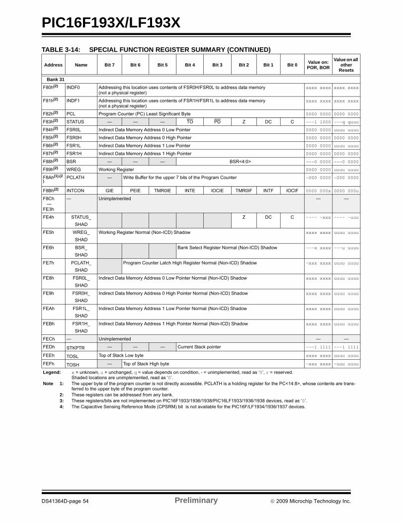
PIC16F193X/LF193X
Bank 31
F80h(2) INDF0 Addressing this location uses contents of FSR0H/FSR0L to address data memory(not a physical register)
xxxx xxxx xxxx xxxx
F81h(2) INDF1 Addressing this location uses contents of FSR1H/FSR1L to address data memory(not a physical register)
xxxx xxxx xxxx xxxx
F82h(2) PCL Program Counter (PC) Least Significant Byte 0000 0000 0000 0000
F83h(2) STATUS — — — TO PD Z DC C ---1 1000 ---q quuu
F84h(2) FSR0L Indirect Data Memory Address 0 Low Pointer 0000 0000 uuuu uuuu
F85h(2) FSR0H Indirect Data Memory Address 0 High Pointer 0000 0000 0000 0000
F86h(2) FSR1L Indirect Data Memory Address 1 Low Pointer 0000 0000 uuuu uuuu
F87h(2) FSR1H Indirect Data Memory Address 1 High Pointer 0000 0000 0000 0000
F88h(2) BSR — — — BSR<4:0> ---0 0000 ---0 0000
F89h(2) WREG Working Register 0000 0000 uuuu uuuu
F8Ah(1),(2
)PCLATH — Write Buffer for the upper 7 bits of the Program Counter -000 0000 -000 0000
F8Bh(2) INTCON GIE PEIE TMR0IE INTE IOCIE TMR0IF INTF IOCIF 0000 000x 0000 000u
F8Ch —FE3h
— Unimplemented — —
FE4h STATUS_
SHAD
Z DC C ---- -xxx ---- -uuu
FE5h WREG_
SHAD
Working Register Normal (Non-ICD) Shadow xxxx xxxx uuuu uuuu
FE6h BSR_
SHAD
Bank Select Register Normal (Non-ICD) Shadow ---x xxxx ---u uuuu
FE7h PCLATH_
SHAD
Program Counter Latch High Register Normal (Non-ICD) Shadow -xxx xxxx uuuu uuuu
FE8h FSR0L_
SHAD
Indirect Data Memory Address 0 Low Pointer Normal (Non-ICD) Shadow xxxx xxxx uuuu uuuu
FE9h FSR0H_
SHAD
Indirect Data Memory Address 0 High Pointer Normal (Non-ICD) Shadow xxxx xxxx uuuu uuuu
FEAh FSR1L_
SHAD
Indirect Data Memory Address 1 Low Pointer Normal (Non-ICD) Shadow xxxx xxxx uuuu uuuu
FEBh FSR1H_
SHAD
Indirect Data Memory Address 1 High Pointer Normal (Non-ICD) Shadow xxxx xxxx uuuu uuuu
FECh — Unimplemented — —
FEDh STKPTR — — — Current Stack pointer ---1 1111 ---1 1111
FEEh TOSL Top of Stack Low byte xxxx xxxx uuuu uuuu
FEFh TOSH — Top of Stack High byte -xxx xxxx -uuu uuuu
TABLE 3-14: SPECIAL FUNCTION REGISTER SUMMARY (CONTINUED)
Address Name Bit 7 Bit 6 Bit 5 Bit 4 Bit 3 Bit 2 Bit 1 Bit 0Value on:POR, BOR
Value on allother
Resets
Legend: x = unknown, u = unchanged, q = value depends on condition, - = unimplemented, read as ‘0’, r = reserved. Shaded locations are unimplemented, read as ‘0’.
Note 1: The upper byte of the program counter is not directly accessible. PCLATH is a holding register for the PC<14:8>, whose contents are trans-ferred to the upper byte of the program counter.
2: These registers can be addressed from any bank.3: These registers/bits are not implemented on PIC16F1933/1936/1938/PIC16LF1933/1936/1938 devices, read as ‘0’.4: The Capacitive Sensing Reference Mode (CPSRM) bit is not available for the PIC16F/LF1934/1936/1937 devices.
DS41364D-page 54 Preliminary 2009 Microchip Technology Inc.

PIC16F193X/LF193X
3.3 PCL and PCLATH
The Program Counter (PC) is 15 bits wide. The low bytecomes from the PCL register, which is a readable andwritable register. The high byte (PC<14:8>) is not directlyreadable or writable and comes from PCLATH. On anyReset, the PC is cleared. Figure 3-5 shows the fivesituations for the loading of the PC.
FIGURE 3-5: LOADING OF PC IN DIFFERENT SITUATIONS
3.3.1 MODIFYING PCL
Executing any instruction with the PCL register as thedestination simultaneously causes the Program Coun-ter PC<14:8> bits (PCH) to be replaced by the contentsof the PCLATH register. This allows the entire contentsof the program counter to be changed by writing thedesired upper 7 bits to the PCLATH register. When thelower 8 bits are written to the PCL register, all 15 bits ofthe program counter will change to the values con-tained in the PCLATH register and those being writtento the PCL register.
3.3.2 COMPUTED GOTO
A computed GOTO is accomplished by adding an offset tothe program counter (ADDWF PCL). When performing atable read using a computed GOTO method, care shouldbe exercised if the table location crosses a PCL memoryboundary (each 256-byte block). Refer to the ApplicationNote AN556, “Implementing a Table Read” (DS00556).
3.3.3 COMPUTED FUNCTION CALLS
A computed function CALL allows programs to maintaintables of functions and provide another way to executestate machines or look-up tables. When performing atable read using a computed function CALL, careshould be exercised if the table location crosses a PCLmemory boundary (each 256-byte block).
If using the CALL instruction, the PCH<2:0> and PCLregisters are loaded with the operand of the CALLinstruction. PCH<6:3> is loaded with PCLATH<6:3>.
The CALLW instruction enables computed calls by com-bining PCLATH and W to form the destination address.A computed CALLW is accomplished by loading the Wregister with the desired address and executing CALLW.The PCL register is loaded with the value of W andPCH is loaded with PCLATH.
3.3.4 BRANCHING
The branching instructions add an offset to the PC.This allows relocatable code and code that crossespage boundaries. There are two forms of branching,BRW and BRA. The PC will have incremented to fetchthe next instruction in both cases. When using eitherbranching instruction, a PCL memory boundary may becrossed.
If using BRW, load the W register with the desiredunsigned address and execute BRW. The entire PC willbe loaded with the address PC + 1 + W.
If using BRA, the entire PC will be loaded with PC + 1 +,the signed value of the operand of the BRA instruction.
PCLPCH 014PC
06 7
ALU Result
8
PCLATH
PCLPCH 014PC
06 4
OPCODE <10:0>11
PCLATH
PCLPCH 014PC
06 7
W8
PCLATH
Instruction with PCL as
Destination
GOTO, CALL
CALLW
PCLPCH 014PC
PC + W15
BRW
PCLPCH 014PC
PC + OPCODE <8:0>15
BRA
2009 Microchip Technology Inc. Preliminary DS41364D-page 55
PIC16F193X/LF193X
3.4 Stack
All devices have a 16-level x 15-bit wide hardwarestack (refer to Figures 3-3 and 3-3). The stack space isnot part of either program or data space. The PC isPUSHed onto the stack when CALL or CALLW instruc-tions are executed or an interrupt causes a branch. Thestack is POPed in the event of a RETURN, RETLW or aRETFIE instruction execution. PCLATH is not affectedby a PUSH or POP operation.
The stack operates as a circular buffer if the STVRENbit = 0 (Configuration Word 2). This means that afterthe stack has been PUSHed sixteen times, the seven-teenth PUSH overwrites the value that was stored fromthe first PUSH. The eighteenth PUSH overwrites thesecond PUSH (and so on). The STKOVF and STKUNFflag bits will be set on an Overflow/Underflow, regard-less of whether the Reset is enabled.
3.4.1 ACCESSING THE STACK
The stack is available through the TOSH, TOSL andSTKPTR registers. STKPTR is the current value of theStack Pointer. TOSH:TOSL register pair points to theTOP of the stack. Both registers are read/writable. TOSis split into TOSH and TOSL due to the 15-bit size of thePC. To access the stack, adjust the value of STKPTR,which will position TOSH:TOSL, then read/write toTOSH:TOSL. STKPTR is 5 bits to allow detection ofoverflow and underflow.
During normal program operation, CALL, CALLW andInterrupts will increment STKPTR while RETLW,RETURN, and RETFIE will decrement STKPTR. At anytime STKPTR can be inspected to see how much stackis left. The STKPTR always points at the currently usedplace on the stack. Therefore, a CALL or CALLW willincrement the STKPTR and then write the PC, and areturn will unload the PC and then decrement the STK-PTR.
Reference Figure 3-6 through Figure 3-9 for examplesof accessing the stack.
FIGURE 3-6: ACCESSING THE STACK EXAMPLE 1
Note 1: There are no instructions/mnemonicscalled PUSH or POP. These are actionsthat occur from the execution of theCALL, CALLW, RETURN, RETLW andRETFIE instructions or the vectoring toan interrupt address.
Note: Care should be taken when modifying theSTKPTR while interrupts are enabled.
0x0F
0x0E
0x0D
0x0C
0x0B
0x0A
0x09
0x08
0x07
0x06
0x05
0x04
0x03
0x02
0x01
0x00
0x0000
STKPTR = 0x1F
Initial Stack Configuration:
After Reset, the stack is empty. Theempty stack is initialized so the StackPointer is pointing at 0x1F. If the StackOverflow/Underflow Reset is enabled, theTOSH/TOSL registers will return ‘0’. Ifthe Stack Overflow/Underflow Reset isdisabled, the TOSH/TOSL registers willreturn the contents of stack address 0x0F.
0x1F STKPTR = 0x1F
Stack Reset Disabled(STVREN = 0)
Stack Reset Enabled(STVREN = 1)
TOSH:TOSL
TOSH:TOSL
DS41364D-page 56 Preliminary 2009 Microchip Technology Inc.
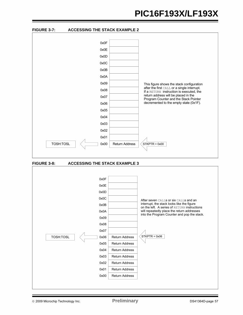
PIC16F193X/LF193X
FIGURE 3-7: ACCESSING THE STACK EXAMPLE 2
FIGURE 3-8: ACCESSING THE STACK EXAMPLE 3
0x0F
0x0E
0x0D
0x0C
0x0B
0x0A
0x09
0x08
0x07
0x06
0x05
0x04
0x03
0x02
0x01
Return Address0x00 STKPTR = 0x00
This figure shows the stack configurationafter the first CALL or a single interrupt.If a RETURN instruction is executed, thereturn address will be placed in theProgram Counter and the Stack Pointerdecremented to the empty state (0x1F).
TOSH:TOSL
0x0F
0x0E
0x0D
0x0C
0x0B
0x0A
0x09
0x08
0x07
Return Address0x06
Return Address0x05
Return Address0x04
Return Address0x03
Return Address0x02
Return Address0x01
Return Address0x00
STKPTR = 0x06
After seven CALLs or six CALLs and aninterrupt, the stack looks like the figureon the left. A series of RETURN instructionswill repeatedly place the return addresses into the Program Counter and pop the stack.
TOSH:TOSL
2009 Microchip Technology Inc. Preliminary DS41364D-page 57

PIC16F193X/LF193X
FIGURE 3-9: ACCESSING THE STACK EXAMPLE 4
3.4.2 OVERFLOW/UNDERFLOW RESET
If the STVREN bit in Configuration Word 2 is set to ‘1’,the device will be reset if the stack is PUSHed beyondthe sixteenth level or POPed beyond the first level,setting the appropriate bits (STKOVF or STKUNF,respectively) in the PCON register.
3.5 Indirect Addressing
The INDFn registers are not physical registers. Anyinstruction that accesses an INDFn register actuallyaccesses the register at the address specified by theFile Select Registers (FSR). If the FSRn addressspecifies one of the two INDFn registers, the read willreturn ‘0’ and the write will not occur (though Status bitsmay be affected). The FSRn register value is createdby the pair FSRnH and FSRnL.
The FSR registers form a 16-bit address that allows anaddressing space with 65536 locations. These locationsare divided into three memory regions:
• Traditional Data Memory
• Linear Data Memory
• Program Flash Memory
0x0F
0x0E
0x0D
0x0C
0x0B
0x0A
0x09
0x08
0x07
0x06
0x05
0x04
0x03
0x02
0x01
Return Address0x00 STKPTR = 0x10
When the stack is full, the next CALL oran interrupt will set the Stack Pointer to0x10. This is identical to address 0x00so the stack will wrap and overwrite thereturn address at 0x00. If the StackOverflow/Underflow Reset is enabled, aReset will occur and location 0x00 willnot be overwritten.
Return Address
Return Address
Return Address
Return Address
Return Address
Return Address
Return Address
Return Address
Return Address
Return Address
Return Address
Return Address
Return Address
Return Address
Return Address
TOSH:TOSL
DS41364D-page 58 Preliminary 2009 Microchip Technology Inc.

PIC16F193X/LF193X
FIGURE 3-10: INDIRECT ADDRESSING
0x0000
0x0FFF
Traditional
FSRAddressRange
Data Memory
0x1000Reserved
LinearData Memory
Reserved
0x2000
0x29AF
0x29B0
0x7FFF
0x8000
0xFFFF
0x0000
0x0FFF
0x0000
0x7FFF
ProgramFlash Memory
Note: Not all memory regions are completely implemented. Consult device memory tables for memory limits.
0x1FFF
2009 Microchip Technology Inc. Preliminary DS41364D-page 59
PIC16F193X/LF193X
3.5.1 TRADITIONAL DATA MEMORY
The traditional data memory is a region from FSRaddress 0x000 to FSR address 0xFFF. The addressescorrespond to the absolute addresses of all SFR, GPRand common registers.
FIGURE 3-11: TRADITIONAL DATA MEMORY MAP
Indirect AddressingDirect Addressing
Bank Select Location Select
4 BSR 6 0From Opcode FSRxL7 0
Bank Select Location Select
0000 0001 0010 11110x00
0x7F
Bank 0 Bank 1 Bank 2 Bank 31
0 FSRxH7 0
0 0 0 0
DS41364D-page 60 Preliminary 2009 Microchip Technology Inc.
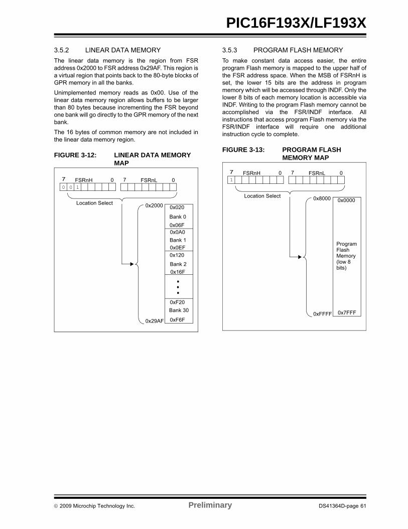
PIC16F193X/LF193X
3.5.2 LINEAR DATA MEMORY
The linear data memory is the region from FSRaddress 0x2000 to FSR address 0x29AF. This region isa virtual region that points back to the 80-byte blocks ofGPR memory in all the banks.
Unimplemented memory reads as 0x00. Use of thelinear data memory region allows buffers to be largerthan 80 bytes because incrementing the FSR beyondone bank will go directly to the GPR memory of the nextbank.
The 16 bytes of common memory are not included inthe linear data memory region.
FIGURE 3-12: LINEAR DATA MEMORY MAP
3.5.3 PROGRAM FLASH MEMORY
To make constant data access easier, the entireprogram Flash memory is mapped to the upper half ofthe FSR address space. When the MSB of FSRnH isset, the lower 15 bits are the address in programmemory which will be accessed through INDF. Only thelower 8 bits of each memory location is accessible viaINDF. Writing to the program Flash memory cannot beaccomplished via the FSR/INDF interface. Allinstructions that access program Flash memory via theFSR/INDF interface will require one additionalinstruction cycle to complete.
FIGURE 3-13: PROGRAM FLASH MEMORY MAP
7
0 170 0
Location Select 0x2000
FSRnH FSRnL
0x020
Bank 0
0x06F0x0A0
Bank 1
0x0EF
0x120
Bank 2
0x16F
0xF20
Bank 30
0xF6F0x29AF
0
7
170 0
Location Select 0x8000
FSRnH FSRnL
0x0000
0x7FFF0xFFFF
ProgramFlashMemory(low 8bits)
2009 Microchip Technology Inc. Preliminary DS41364D-page 61

PIC16F193X/LF193X
NOTES:
DS41364D-page 62 Preliminary 2009 Microchip Technology Inc.
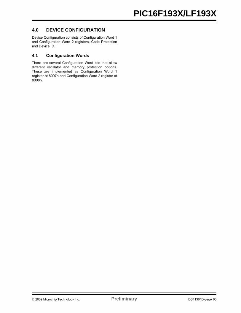
PIC16F193X/LF193X
4.0 DEVICE CONFIGURATION
Device Configuration consists of Configuration Word 1and Configuration Word 2 registers, Code Protectionand Device ID.
4.1 Configuration Words
There are several Configuration Word bits that allowdifferent oscillator and memory protection options.These are implemented as Configuration Word 1register at 8007h and Configuration Word 2 register at8008h.
2009 Microchip Technology Inc. Preliminary DS41364D-page 63
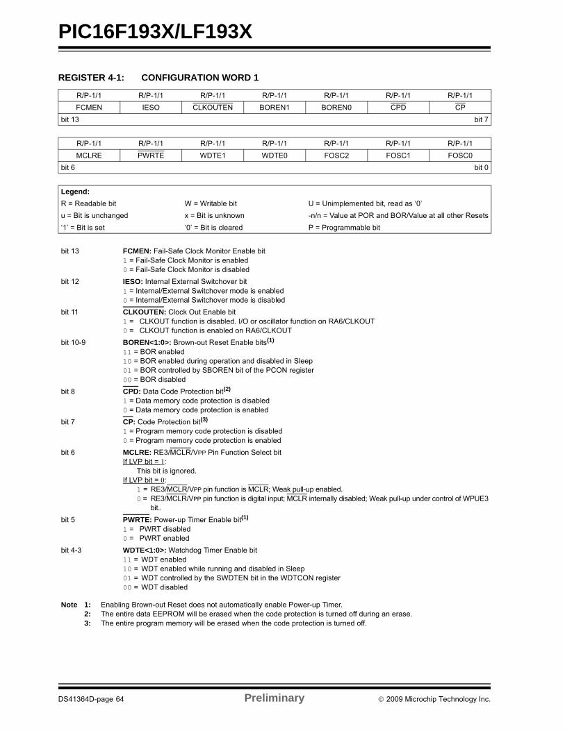
PIC16F193X/LF193X
REGISTER 4-1: CONFIGURATION WORD 1
R/P-1/1 R/P-1/1 R/P-1/1 R/P-1/1 R/P-1/1 R/P-1/1 R/P-1/1
FCMEN IESO CLKOUTEN BOREN1 BOREN0 CPD CP
bit 13 bit 7
R/P-1/1 R/P-1/1 R/P-1/1 R/P-1/1 R/P-1/1 R/P-1/1 R/P-1/1
MCLRE PWRTE WDTE1 WDTE0 FOSC2 FOSC1 FOSC0
bit 6 bit 0
Legend:
R = Readable bit W = Writable bit U = Unimplemented bit, read as ‘0’
u = Bit is unchanged x = Bit is unknown -n/n = Value at POR and BOR/Value at all other Resets
‘1’ = Bit is set ‘0’ = Bit is cleared P = Programmable bit
bit 13 FCMEN: Fail-Safe Clock Monitor Enable bit1 = Fail-Safe Clock Monitor is enabled0 = Fail-Safe Clock Monitor is disabled
bit 12 IESO: Internal External Switchover bit1 = Internal/External Switchover mode is enabled0 = Internal/External Switchover mode is disabled
bit 11 CLKOUTEN: Clock Out Enable bit1 = CLKOUT function is disabled. I/O or oscillator function on RA6/CLKOUT0 = CLKOUT function is enabled on RA6/CLKOUT
bit 10-9 BOREN<1:0>: Brown-out Reset Enable bits(1)
11 = BOR enabled10 = BOR enabled during operation and disabled in Sleep01 = BOR controlled by SBOREN bit of the PCON register00 = BOR disabled
bit 8 CPD: Data Code Protection bit(2)
1 = Data memory code protection is disabled0 = Data memory code protection is enabled
bit 7 CP: Code Protection bit(3)
1 = Program memory code protection is disabled0 = Program memory code protection is enabled
bit 6 MCLRE: RE3/MCLR/VPP Pin Function Select bitIf LVP bit = 1:
This bit is ignored.If LVP bit = 0:
1 = RE3/MCLR/VPP pin function is MCLR; Weak pull-up enabled.0 = RE3/MCLR/VPP pin function is digital input; MCLR internally disabled; Weak pull-up under control of WPUE3
bit..
bit 5 PWRTE: Power-up Timer Enable bit(1)
1 = PWRT disabled0 = PWRT enabled
bit 4-3 WDTE<1:0>: Watchdog Timer Enable bit11 = WDT enabled10 = WDT enabled while running and disabled in Sleep01 = WDT controlled by the SWDTEN bit in the WDTCON register00 = WDT disabled
Note 1: Enabling Brown-out Reset does not automatically enable Power-up Timer.2: The entire data EEPROM will be erased when the code protection is turned off during an erase.3: The entire program memory will be erased when the code protection is turned off.
DS41364D-page 64 Preliminary 2009 Microchip Technology Inc.
PIC16F193X/LF193X
bit 2-0 FOSC<2:0>: Oscillator Selection bits111 = ECH: External Clock, High-Power mode: CLKIN on RA7/OSC1/CLKIN110 = ECM: External Clock, Medium-Power mode: CLKIN on RA7/OSC1/CLKIN101 = ECL: External Clock, Low-Power mode: CLKIN on RA7/OSC1/CLKIN100 = INTOSC oscillator: I/O function on RA7/OSC1/CLKIN011 = EXTRC oscillator: RC function on RA7/OSC1/CLKIN010 = HS oscillator: High-speed crystal/resonator on RA6/OSC2/CLKOUT pin and RA7/OSC1/CLKIN001 = XT oscillator: Crystal/resonator on RA6/OSC2/CLKOUT pin and RA7/OSC1/CLKIN000 = LP oscillator: Low-power crystal on RA6/OSC2/CLKOUT pin and RA7/OSC1/CLKIN
REGISTER 4-1: CONFIGURATION WORD 1 (CONTINUED)
Note 1: Enabling Brown-out Reset does not automatically enable Power-up Timer.2: The entire data EEPROM will be erased when the code protection is turned off during an erase.3: The entire program memory will be erased when the code protection is turned off.
2009 Microchip Technology Inc. Preliminary DS41364D-page 65
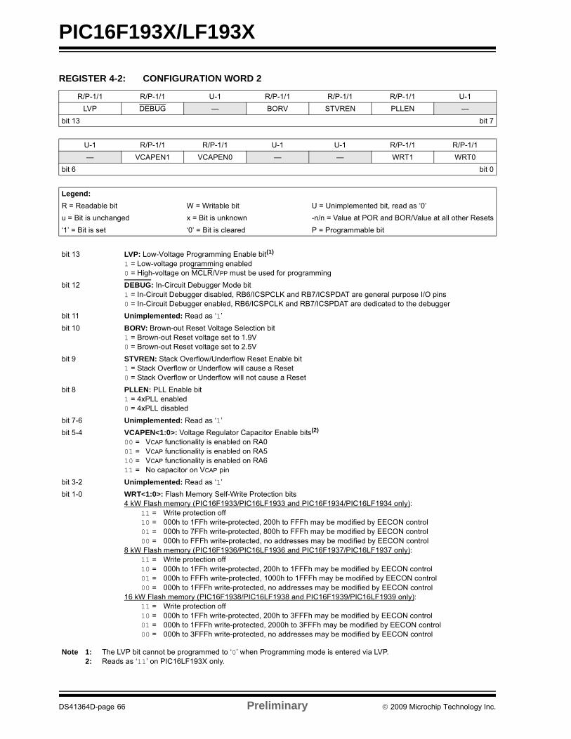
PIC16F193X/LF193X
REGISTER 4-2: CONFIGURATION WORD 2
R/P-1/1 R/P-1/1 U-1 R/P-1/1 R/P-1/1 R/P-1/1 U-1
LVP DEBUG — BORV STVREN PLLEN —
bit 13 bit 7
U-1 R/P-1/1 R/P-1/1 U-1 U-1 R/P-1/1 R/P-1/1
— VCAPEN1 VCAPEN0 — — WRT1 WRT0
bit 6 bit 0
Legend:
R = Readable bit W = Writable bit U = Unimplemented bit, read as ‘0’
u = Bit is unchanged x = Bit is unknown -n/n = Value at POR and BOR/Value at all other Resets
‘1’ = Bit is set ‘0’ = Bit is cleared P = Programmable bit
bit 13 LVP: Low-Voltage Programming Enable bit(1)
1 = Low-voltage programming enabled0 = High-voltage on MCLR/VPP must be used for programming
bit 12 DEBUG: In-Circuit Debugger Mode bit1 = In-Circuit Debugger disabled, RB6/ICSPCLK and RB7/ICSPDAT are general purpose I/O pins0 = In-Circuit Debugger enabled, RB6/ICSPCLK and RB7/ICSPDAT are dedicated to the debugger
bit 11 Unimplemented: Read as ‘1’
bit 10 BORV: Brown-out Reset Voltage Selection bit1 = Brown-out Reset voltage set to 1.9V0 = Brown-out Reset voltage set to 2.5V
bit 9 STVREN: Stack Overflow/Underflow Reset Enable bit1 = Stack Overflow or Underflow will cause a Reset0 = Stack Overflow or Underflow will not cause a Reset
bit 8 PLLEN: PLL Enable bit1 = 4xPLL enabled0 = 4xPLL disabled
bit 7-6 Unimplemented: Read as ‘1’
bit 5-4 VCAPEN<1:0>: Voltage Regulator Capacitor Enable bits(2)
00 = VCAP functionality is enabled on RA001 = VCAP functionality is enabled on RA510 = VCAP functionality is enabled on RA611 = No capacitor on VCAP pin
bit 3-2 Unimplemented: Read as ‘1’
bit 1-0 WRT<1:0>: Flash Memory Self-Write Protection bits4 kW Flash memory (PIC16F1933/PIC16LF1933 and PIC16F1934/PIC16LF1934 only):
11 = Write protection off10 = 000h to 1FFh write-protected, 200h to FFFh may be modified by EECON control01 = 000h to 7FFh write-protected, 800h to FFFh may be modified by EECON control00 = 000h to FFFh write-protected, no addresses may be modified by EECON control
8 kW Flash memory (PIC16F1936/PIC16LF1936 and PIC16F1937/PIC16LF1937 only):11 = Write protection off10 = 000h to 1FFh write-protected, 200h to 1FFFh may be modified by EECON control01 = 000h to FFFh write-protected, 1000h to 1FFFh may be modified by EECON control00 = 000h to 1FFFh write-protected, no addresses may be modified by EECON control
16 kW Flash memory (PIC16F1938/PIC16LF1938 and PIC16F1939/PIC16LF1939 only):11 = Write protection off10 = 000h to 1FFh write-protected, 200h to 3FFFh may be modified by EECON control01 = 000h to 1FFFh write-protected, 2000h to 3FFFh may be modified by EECON control00 = 000h to 3FFFh write-protected, no addresses may be modified by EECON control
Note 1: The LVP bit cannot be programmed to ‘0’ when Programming mode is entered via LVP.2: Reads as ‘11’ on PIC16LF193X only.
DS41364D-page 66 Preliminary 2009 Microchip Technology Inc.
PIC16F193X/LF193X
4.2 Code Protection
Code protection allows the device to be protected fromunauthorized access. Program memory protection anddata EEPROM protection are controlled independently.Internal access to the program memory and dataEEPROM are unaffected by any code protectionsetting.
4.2.1 PROGRAM MEMORY PROTECTION
The entire program memory space is protected fromexternal reads and writes by the CP bit in ConfigurationWord 1. When CP = 0, external reads and writes ofprogram memory are inhibited and a read will return all‘0’s. The CPU can continue to read program memory,regardless of the protection bit settings. Writing theprogram memory is dependent upon the writeprotection setting. See Section 4.3 “WriteProtection” for more information.
4.2.2 DATA EEPROM PROTECTION
The entire data EEPROM is protected from externalreads and writes by the CPD bit. When CPD = 0,external reads and writes of data EEPROM areinhibited. The CPU can continue to read and write dataEEPROM regardless of the protection bit settings.
4.3 Write Protection
Write protection allows the device to be protected fromunintended self-writes. Applications, such asbootloader software, can be protected while allowingother regions of the program memory to be modified.
The WRT<1:0> bits in Configuration Word 2 define thesize of the program memory block that is protected.
4.4 User ID
Four memory locations (8000h-8003h) are designatedas ID locations where the user can store checksum orother code identification numbers. These locations arereadable and writable during normal execution. SeeSection 4.5 “Device ID and Revision ID” for moreinformation on accessing these memory locations. Formore information on checksum calculation, see the“PIC16193X/PIC16LF193X Memory ProgrammingSpecification” (DS41360).
2009 Microchip Technology Inc. Preliminary DS41364D-page 67
PIC16F193X/LF193X
4.5 Device ID and Revision ID
The memory location 8006h is where the Device ID andRevision ID are stored. The upper nine bits hold theDevice ID. The lower five bits hold the Revision ID. SeeSection 11.5 “User ID, Device ID and ConfigurationWord Access” for more information on accessingthese memory locations.
Development tools, such as device programmers anddebuggers, may be used to read the Device ID andRevision ID.
REGISTER 4-3: DEVICEID: DEVICE ID REGISTER(1)
R R R R R R R
DEV8 DEV7 DEV6 DEV5 DEV4 DEV3 DEV2
bit 13 bit 7
R R R R R R R
DEV1 DEV0 REV4 REV3 REV2 REV1 REV0
bit 6 bit 0
Legend: U = Unimplemented bit, read as ‘0’
R = Readable bit W = Writable bit ‘0’ = Bit is cleared
-n = Value at POR ‘1’ = Bit is set x = Bit is unknown
bit 13-5 DEV<8:0>: Device ID bits100011001 = PIC16F1933100011010 = PIC16F1934100011011 = PIC16F1936100011100 = PIC16F1937100011101 = PIC16F1938100011110 = PIC16F1939100100001 = PIC16LF1933100100010 = PIC16LF1934100100011 = PIC16LF1936100100100 = PIC16LF1937100100101 = PIC16LF1938100100110 = PIC16LF1939
bit 4-0 REV<4:0>: Revision ID bits
These bits are used to identify the revision.
Note 1: This location cannot be written.
DS41364D-page 68 Preliminary 2009 Microchip Technology Inc.
PIC16F193X/LF193X
5.0 OSCILLATOR MODULE (WITH FAIL-SAFE CLOCK MONITOR)
5.1 Overview
The oscillator module has a wide variety of clocksources and selection features that allow it to be usedin a wide range of applications while maximizing perfor-mance and minimizing power consumption. Figure 5-1illustrates a block diagram of the oscillator module.
Clock sources can be supplied from external oscillators,quartz crystal resonators, ceramic resonators andResistor-Capacitor (RC) circuits. In addition, the systemclock source can be supplied from one of two internaloscillators and PLL circuits, with a choice of speedsselectable via software. Additional clock featuresinclude:
• Selectable system clock source between external or internal sources via software.
• Two-Speed Start-up mode, which minimizes latency between external oscillator start-up and code execution.
• Fail-Safe Clock Monitor (FSCM) designed to detect a failure of the external clock source (LP, XT, HS, EC or RC modes) and switch automatically to the internal oscillator.
• Oscillator Start-up Timer (OST) ensures stability of crystal oscillator sources
The oscillator module can be configured in one of sixclock modes.
1. EC – External clock.
2. LP – 32 kHz Low-Power Crystal mode.
3. XT – Medium Gain Crystal or Ceramic ResonatorOscillator mode.
4. HS – High Gain Crystal or Ceramic Resonatormode.
5. RC – External Resistor-Capacitor (RC).
6. INTOSC – Internal oscillator.
Clock Source modes are selected by the FOSC<2:0>bits in the Configuration Word 1. The FOSC bitsdetermine the type of oscillator that will be used whenthe device is first powered.
The EC clock mode relies on an external logic levelsignal as the device clock source. The LP, XT, and HSclock modes require an external crystal or resonator tobe connected to the device. Each mode is optimized fora different frequency range. The RC clock moderequires an external resistor and capacitor to set theoscillator frequency.
The INTOSC internal oscillator block produces low,medium, and high frequency clock sources, designatedLFINTOSC, MFINTOSC, and HFINTOSC. (seeInternal Oscillator Block, Figure 5-1). A wide selectionof device clock frequencies may be derived from thesethree clock sources.
FIGURE 5-1: SIMPLIFIED PIC® MCU CLOCK SOURCE BLOCK DIAGRAM
4 x PLL
FOSC<2:0>
Oscillator
T1OSCENEnableOscillator
T1OSO
T1OSI
Clock Source Option for other modules
OSC1
OSC2
Sleep
LP, XT, HS, RC, EC
T1OSC CPU and
Po
stsc
ale
r
MU
X
MU
X
16 MHz8 MHz4 MHz2 MHz1 MHz
250 kHz500 kHz
IRCF<3:0>
31 kHz
500 kHzSource
InternalOscillator
Block
WDT, PWRT, Fail-Safe Clock Monitor
16 MHz
Internal Oscillator
(HFINTOSC)
ClockControl
SCS<1:0>
HFPLL
31 kHz (LFINTOSC)Two-Speed Start-up and other modules
Oscillator
31 kHzSource
500 kHz(MFINTOSC)
125 kHz
31.25 kHz62.5 kHz
FOSC<2:0> = 100 Peripherals
Sleep
External
Timer1
2009 Microchip Technology Inc. Preliminary DS41364D-page 69
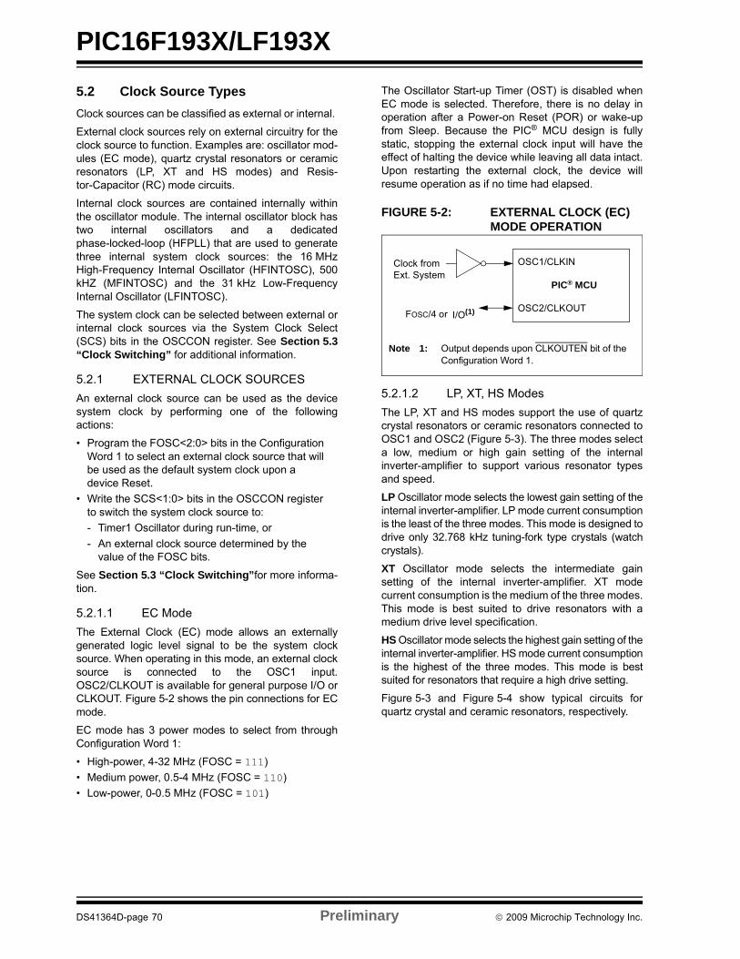
PIC16F193X/LF193X
5.2 Clock Source Types
Clock sources can be classified as external or internal.
External clock sources rely on external circuitry for theclock source to function. Examples are: oscillator mod-ules (EC mode), quartz crystal resonators or ceramicresonators (LP, XT and HS modes) and Resis-tor-Capacitor (RC) mode circuits.
Internal clock sources are contained internally withinthe oscillator module. The internal oscillator block hastwo internal oscillators and a dedicatedphase-locked-loop (HFPLL) that are used to generatethree internal system clock sources: the 16 MHzHigh-Frequency Internal Oscillator (HFINTOSC), 500kHZ (MFINTOSC) and the 31 kHz Low-FrequencyInternal Oscillator (LFINTOSC).
The system clock can be selected between external orinternal clock sources via the System Clock Select(SCS) bits in the OSCCON register. See Section 5.3“Clock Switching” for additional information.
5.2.1 EXTERNAL CLOCK SOURCES
An external clock source can be used as the devicesystem clock by performing one of the followingactions:
• Program the FOSC<2:0> bits in the Configuration Word 1 to select an external clock source that will be used as the default system clock upon a device Reset.
• Write the SCS<1:0> bits in the OSCCON register to switch the system clock source to:
- Timer1 Oscillator during run-time, or
- An external clock source determined by the value of the FOSC bits.
See Section 5.3 “Clock Switching”for more informa-tion.
5.2.1.1 EC Mode
The External Clock (EC) mode allows an externallygenerated logic level signal to be the system clocksource. When operating in this mode, an external clocksource is connected to the OSC1 input.OSC2/CLKOUT is available for general purpose I/O orCLKOUT. Figure 5-2 shows the pin connections for ECmode.
EC mode has 3 power modes to select from throughConfiguration Word 1:
• High-power, 4-32 MHz (FOSC = 111)
• Medium power, 0.5-4 MHz (FOSC = 110)
• Low-power, 0-0.5 MHz (FOSC = 101)
The Oscillator Start-up Timer (OST) is disabled whenEC mode is selected. Therefore, there is no delay inoperation after a Power-on Reset (POR) or wake-upfrom Sleep. Because the PIC® MCU design is fullystatic, stopping the external clock input will have theeffect of halting the device while leaving all data intact.Upon restarting the external clock, the device willresume operation as if no time had elapsed.
FIGURE 5-2: EXTERNAL CLOCK (EC) MODE OPERATION
5.2.1.2 LP, XT, HS Modes
The LP, XT and HS modes support the use of quartzcrystal resonators or ceramic resonators connected toOSC1 and OSC2 (Figure 5-3). The three modes selecta low, medium or high gain setting of the internalinverter-amplifier to support various resonator typesand speed.
LP Oscillator mode selects the lowest gain setting of theinternal inverter-amplifier. LP mode current consumptionis the least of the three modes. This mode is designed todrive only 32.768 kHz tuning-fork type crystals (watchcrystals).
XT Oscillator mode selects the intermediate gainsetting of the internal inverter-amplifier. XT modecurrent consumption is the medium of the three modes.This mode is best suited to drive resonators with amedium drive level specification.
HS Oscillator mode selects the highest gain setting of theinternal inverter-amplifier. HS mode current consumptionis the highest of the three modes. This mode is bestsuited for resonators that require a high drive setting.
Figure 5-3 and Figure 5-4 show typical circuits forquartz crystal and ceramic resonators, respectively.
OSC1/CLKIN
OSC2/CLKOUT
Clock fromExt. System
PIC® MCU
FOSC/4 or I/O(1)
Note 1: Output depends upon CLKOUTEN bit of the Configuration Word 1.
DS41364D-page 70 Preliminary 2009 Microchip Technology Inc.

PIC16F193X/LF193X
FIGURE 5-3: QUARTZ CRYSTAL OPERATION (LP, XT OR HS MODE)
FIGURE 5-4: CERAMIC RESONATOR OPERATION(XT OR HS MODE)
5.2.1.3 Oscillator Start-up Timer (OST)
If the oscillator module is configured for LP, XT or HSmodes, the Oscillator Start-up Timer (OST) counts1024 oscillations from OSC1. This occurs following aPower-on Reset (POR) and when the Power-up Timer(PWRT) has expired (if configured), or a wake-up fromSleep. During this time, the program counter does notincrement and program execution is suspended. TheOST ensures that the oscillator circuit, using a quartzcrystal resonator or ceramic resonator, has started andis providing a stable system clock to the oscillatormodule.
In order to minimize latency between external oscillatorstart-up and code execution, the Two-Speed ClockStart-up mode can be selected (see Section 5.4“Two-Speed Clock Start-up Mode”).
5.2.1.4 4X PLL
The oscillator module contains a 4X PLL that can beused with both external and internal clock sources toprovide a system clock source. The input frequency forthe 4X PLL must fall within specifications. See the PLLClock Timing Specifications in Section 29.0“Electrical Specifications”.
The 4X PLL may be enabled for use by one of twomethods:
1. Program the PLLEN bit in Configuration Word 2to a ‘1’.
2. Write the SPLLEN bit in the OSCCON register toa ‘1’. If the PLLEN bit in Configuration Word 2 isprogrammed to a ‘1’, then the value of SPLLENis ignored.
Note 1: Quartz crystal characteristics vary accordingto type, package and manufacturer. Theuser should consult the manufacturer datasheets for specifications and recommendedapplication.
2: Always verify oscillator performance overthe VDD and temperature range that isexpected for the application.
3: For oscillator design assistance, referencethe following Microchip Applications Notes:
• AN826, “Crystal Oscillator Basics and Crystal Selection for rfPIC® and PIC® Devices” (DS00826)
• AN849, “Basic PIC® Oscillator Design” (DS00849)
• AN943, “Practical PIC® Oscillator Analysis and Design” (DS00943)
• AN949, “Making Your Oscillator Work” (DS00949)
Note 1: A series resistor (RS) may be required forquartz crystals with low drive level.
2: The value of RF varies with the Oscillator modeselected (typically between 2 M to 10 M.
C1
C2
Quartz
RS(1)
OSC1/CLKIN
RF(2) Sleep
To Internal Logic
PIC® MCU
Crystal
OSC2/CLKOUT
Note 1: A series resistor (RS) may be required forceramic resonators with low drive level.
2: The value of RF varies with the Oscillator modeselected (typically between 2 M to 10 M.
3: An additional parallel feedback resistor (RP)may be required for proper ceramic resonatoroperation.
C1
C2 Ceramic RS(1)
OSC1/CLKIN
RF(2) Sleep
To Internal Logic
PIC® MCU
RP(3)
Resonator
OSC2/CLKOUT
2009 Microchip Technology Inc. Preliminary DS41364D-page 71
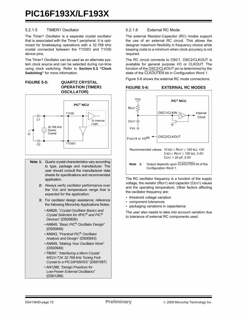
PIC16F193X/LF193X
5.2.1.5 TIMER1 Oscillator
The Timer1 Oscillator is a separate crystal oscillatorthat is associated with the Timer1 peripheral. It is opti-mized for timekeeping operations with a 32.768 kHzcrystal connected between the T1OSO and T1OSIdevice pins.
The Timer1 Oscillator can be used as an alternate sys-tem clock source and can be selected during run-timeusing clock switching. Refer to Section 5.3 “ClockSwitching” for more information.
FIGURE 5-5: QUARTZ CRYSTAL OPERATION (TIMER1 OSCILLATOR)
5.2.1.6 External RC Mode
The external Resistor-Capacitor (RC) modes supportthe use of an external RC circuit. This allows thedesigner maximum flexibility in frequency choice whilekeeping costs to a minimum when clock accuracy is notrequired.
The RC circuit connects to OSC1. OSC2/CLKOUT isavailable for general purpose I/O or CLKOUT. Thefunction of the OSC2/CLKOUT pin is determined by thestate of the CLKOUTEN bit in Configuration Word 1.
Figure 5-6 shows the external RC mode connections.
FIGURE 5-6: EXTERNAL RC MODES
The RC oscillator frequency is a function of the supplyvoltage, the resistor (REXT) and capacitor (CEXT) valuesand the operating temperature. Other factors affectingthe oscillator frequency are:
• threshold voltage variation• component tolerances• packaging variations in capacitance
The user also needs to take into account variation dueto tolerance of external RC components used.
Note 1: Quartz crystal characteristics vary accordingto type, package and manufacturer. Theuser should consult the manufacturer datasheets for specifications and recommendedapplication.
2: Always verify oscillator performance overthe VDD and temperature range that isexpected for the application.
3: For oscillator design assistance, referencethe following Microchip Applications Notes:
• AN826, “Crystal Oscillator Basics and Crystal Selection for rfPIC® and PIC® Devices” (DS00826)
• AN849, “Basic PIC® Oscillator Design” (DS00849)
• AN943, “Practical PIC® Oscillator Analysis and Design” (DS00943)
• AN949, “Making Your Oscillator Work” (DS00949)
• TB097, “Interfacing a Micro Crystal MS1V-T1K 32.768 kHz Tuning Fork Crystal to a PIC16F690/SS” (DS91097)
• AN1288, “Design Practices for Low-Power External Oscillators” (DS01288)
C1
C2
32.768 kHz
T1OSI
To Internal Logic
PIC® MCU
Crystal
T1OSO
Quartz
OSC2/CLKOUT
CEXT
REXT
PIC® MCU
OSC1/CLKIN
FOSC/4 or
InternalClock
VDD
VSS
Recommended values: 10 k REXT 100 k, <3V3 k REXT 100 k, 3-5VCEXT > 20 pF, 2-5V
Note 1: Output depends upon CLKOUTEN bit of the Configuration Word 1.
I/O(1)
DS41364D-page 72 Preliminary 2009 Microchip Technology Inc.
PIC16F193X/LF193X
5.2.2 INTERNAL CLOCK SOURCES
The device may be configured to use the internal oscil-lator block as the system clock by performing one of thefollowing actions:
• Program the FOSC<2:0> bits in Configuration Word 1 to select the INTOSC clock source, which will be used as the default system clock upon a device Reset.
• Write the SCS<1:0> bits in the OSCCON register to switch the system clock source to the internal oscillator during run-time. See Section 5.3 “Clock Switching”for more information.
In INTOSC mode, OSC1/CLKIN is available for generalpurpose I/O. OSC2/CLKOUT is available for generalpurpose I/O or CLKOUT.
The function of the OSC2/CLKOUT pin is determinedby the state of the CLKOUTEN bit in ConfigurationWord 1.
The internal oscillator block has two independentoscillators and a dedicated Phase-Locked Loop,HFPLL that can produce one of three internal systemclock sources.
1. The HFINTOSC (High-Frequency InternalOscillator) is factory calibrated and operates at16 MHz. The HFINTOSC source is generatedfrom the 500 kHz MFINTOSC source and thededicated Phase-Locked Loop, HFPLL. Thefrequency of the HFINTOSC can beuser-adjusted via software using the OSCTUNEregister (Register 5-3).
2. The MFINTOSC (Medium-Frequency InternalOscillator) is factory calibrated and operates at500 kHz. The frequency of the MFINTOSC canbe user-adjusted via software using theOSCTUNE register (Register 5-3).
3. The LFINTOSC (Low-Frequency InternalOscillator) is uncalibrated and operates at31 kHz.
5.2.2.1 HFINTOSC
The High-Frequency Internal Oscillator (HFINTOSC) isa factory calibrated 16 MHz internal clock source. Thefrequency of the HFINTOSC can be altered viasoftware using the OSCTUNE register (Register 5-3).
The output of the HFINTOSC connects to a postscalerand multiplexer (see Figure 5-1). One of ninefrequencies derived from the HFINTOSC can beselected via software using the IRCF<3:0> bits of theOSCCON register. See Section 5.2.2.7 “InternalOscillator Clock Switch Timing” for more information.
The HFINTOSC is enabled by:
• Configure the IRCF<3:0> bits of the OSCCON register for the desired HF frequency, and
• FOSC<2:0> = 100, or
• Set the System Clock Source (SCS) bits of the OSCCON register to ‘1x’.
The High Frequency Internal Oscillator Ready bit(HFIOFR) of the OSCSTAT register indicates when theHFINTOSC is running and can be utilized.
The High Frequency Internal Oscillator Status Lockedbit (HFIOFL) of the OSCSTAT register indicates whenthe HFINTOSC is running within 2% of its final value.
The High Frequency Internal Oscillator Status Stablebit (HFIOFS) of the OSCSTAT register indicates whenthe HFINTOSC is running within 0.5% of its final value.
5.2.2.2 MFINTOSC
The Medium-Frequency Internal Oscillator(MFINTOSC) is a factory calibrated 500 kHz internalclock source. The frequency of the MFINTOSC can bealtered via software using the OSCTUNE register(Register 5-3).
The output of the MFINTOSC connects to a postscalerand multiplexer (see Figure 5-1). One of ninefrequencies derived from the MFINTOSC can beselected via software using the IRCF<3:0> bits of theOSCCON register. See Section 5.2.2.7 “InternalOscillator Clock Switch Timing” for more information.
The MFINTOSC is enabled by:
• Configure the IRCF<3:0> bits of the OSCCON register for the desired HF frequency, and
• FOSC<2:0> = 100, or
• Set the System Clock Source (SCS) bits of the OSCCON register to ‘1x’
The Medium Frequency Internal Oscillator Ready bit(MFIOFR) of the OSCSTAT register indicates when theMFINTOSC is running and can be utilized.
2009 Microchip Technology Inc. Preliminary DS41364D-page 73
PIC16F193X/LF193X
5.2.2.3 Internal Oscillator Frequency Adjustment
The 500 kHz internal oscillator is factory calibrated.This internal oscillator can be adjusted in software bywriting to the OSCTUNE register (Register 5-3). Sincethe HFINTOSC and MFINTOSC clock sources arederived from the 500 kHz internal oscillator a change inthe OSCTUNE register value will apply to both.
The default value of the OSCTUNE register is ‘0’. Thevalue is a 5-bit two’s complement number. A value of0Fh will provide an adjustment to the maximumfrequency. A value of 10h will provide an adjustment tothe minimum frequency.
When the OSCTUNE register is modified, the oscillatorfrequency will begin shifting to the new frequency. Codeexecution continues during this shift. There is noindication that the shift has occurred.
OSCTUNE does not affect the LFINTOSC frequency.Operation of features that depend on the LFINTOSCclock source frequency, such as the Power-up Timer(PWRT), Watchdog Timer (WDT), Fail-Safe ClockMonitor (FSCM) and peripherals, are not affected by thechange in frequency.
5.2.2.4 LFINTOSC
The Low-Frequency Internal Oscillator (LFINTOSC) isan uncalibrated 31 kHz internal clock source.
The output of the LFINTOSC connects to a postscalerand multiplexer (see Figure 5-1). Select 31 kHz, viasoftware, using the IRCF<3:0> bits of the OSCCONregister. See Section 5.2.2.7 “Internal OscillatorClock Switch Timing” for more information. TheLFINTOSC is also the frequency for the Power-up Timer(PWRT), Watchdog Timer (WDT) and Fail-Safe ClockMonitor (FSCM).
The LFINTOSC is enabled by selecting 31 kHz(IRCF<3:0> bits of the OSCCON register = 000) as thesystem clock source (SCS bits of the OSCCONregister = 1x), or when any of the following areenabled:
• Configure the IRCF<3:0> bits of the OSCCON register for the desired LF frequency, and
• FOSC<2:0> = 100, or
• Set the System Clock Source (SCS) bits of the OSCCON register to ‘1x’
Peripherals that use the LFINTOSC are:
• Power-up Timer (PWRT)
• Watchdog Timer (WDT)
• Fail-Safe Clock Monitor (FSCM)
The Low Frequency Internal Oscillator Ready bit(LFIOFR) of the OSCSTAT register indicates when theLFINTOSC is running and can be utilized.
5.2.2.5 Internal Oscillator Frequency Selection
The system clock speed can be selected via softwareusing the Internal Oscillator Frequency Select bitsIRCF<3:0> of the OSCCON register.
The output of the 16 MHz HFINTOSC and 31 kHzLFINTOSC connects to a postscaler and multiplexer(see Figure 5-1). The Internal Oscillator FrequencySelect bits IRCF<3:0> of the OSCCON register selectthe frequency output of the internal oscillators. One ofthe following frequencies can be selected via software:
• 32 MHz (requires 4X PLL)
• 16 MHz
• 8 MHz
• 4 MHz
• 2 MHz
• 1 MHz
• 500 kHz (Default after Reset)
• 250 kHz
• 125 kHz
• 62.5 kHz
• 31.25 kHz
• 31 kHz (LFINTOSC)
The IRCF<3:0> bits of the OSCCON register allowduplicate selections for some frequencies. These dupli-cate choices can offer system design trade-offs. Lowerpower consumption can be obtained when changingoscillator sources for a given frequency. Faster transi-tion times can be obtained between frequency changesthat use the same oscillator source.
Note: Following any Reset, the IRCF<3:0> bits ofthe OSCCON register are set to ‘0111’ andthe frequency selection is set to 500 kHz.The user can modify the IRCF bits toselect a different frequency.
DS41364D-page 74 Preliminary 2009 Microchip Technology Inc.

PIC16F193X/LF193X
5.2.2.6 32 MHz Internal Oscillator Frequency Selection
The Internal Oscillator Block can be used with the 4XPLL associated with the External Oscillator Block toproduce a 32 MHz internal system clock source. Thefollowing settings are required to use the 32 MHz inter-nal clock source:
• The FOSC bits in Configuration Word 1 must be set to use the INTOSC source as the device sys-tem clock (FOSC<2:0> = 100).
• The IRCF bits in the OSCCON register must be set to the 8 MHz HFINTOSC selection (IRCF<3:0> = 1110).
• The SPLLEN bit in the OSCCON register must be set to enable the 4X PLL.
5.2.2.7 Internal Oscillator Clock Switch Timing
When switching between the HFINTOSC, MFINTOSCand the LFINTOSC, the new oscillator may already beshut down to save power (see Figure 5-7). If this is thecase, there is a delay after the IRCF<3:0> bits of theOSCCON register are modified before the frequencyselection takes place. The OSCSTAT register willreflect the current active status of the HFINTOSC,MFINTOSC and LFINTOSC oscillators. The sequenceof a frequency selection is as follows:
1. IRCF<3:0> bits of the OSCCON register aremodified.
2. If the new clock is shut down, a clock start-updelay is started.
3. Clock switch circuitry waits for a falling edge ofthe current clock.
4. The current clock is held low and the clockswitch circuitry waits for a rising edge in the newclock.
5. The new clock is now active.
6. The OSCSTAT register is updated as required.
7. Clock switch is complete.
See Figure 5-7 for more details.
If the internal oscillator speed is switched between twoclocks of the same source, there is no start-up delaybefore the new frequency is selected. Clock switchingtime delays are shown in Table 5-1.
Start-up delay specifications are located in theoscillator tables of Section 29.0 “ElectricalSpecifications”.
Note: The 4X PLL may also be enabled for usewith the Internal Oscillator Block byprogramming the PLLEN bit inConfiguration Word 2 to a ‘1’. However,the 4X PLL cannot be disabled bysoftware and the 8 MHz HFINTOSCoption will no longer be available.
2009 Microchip Technology Inc. Preliminary DS41364D-page 75

PIC16F193X/LF193X
FIGURE 5-7: INTERNAL OSCILLATOR SWITCH TIMING
HFINTOSC/
LFINTOSC
IRCF <3:0>
System Clock
HFINTOSC/
LFINTOSC
IRCF <3:0>
System Clock
0 0
0 0
Start-up Time 2-cycle Sync Running
2-cycle Sync Running
HFINTOSC/ LFINTOSC (FSCM and WDT disabled)
HFINTOSC/ LFINTOSC (Either FSCM or WDT enabled)
LFINTOSC
HFINTOSC/
IRCF <3:0>
System Clock
= 0 0
Start-up Time 2-cycle Sync Running
LFINTOSC HFINTOSC/MFINTOSCLFINTOSC turns off unless WDT or FSCM is enabled
MFINTOSC
MFINTOSC
MFINTOSC
MFINTOSC
MFINTOSC
DS41364D-page 76 Preliminary 2009 Microchip Technology Inc.
PIC16F193X/LF193X
5.3 Clock Switching
The system clock source can be switched betweenexternal and internal clock sources via software usingthe System Clock Select (SCS) bits of the OSCCONregister. The following clock sources can be selectedusing the SCS bits:
• Default system oscillator determined by FOSC bits in Configuration Word 1
• Timer1 32 kHz crystal oscillator
• Internal Oscillator Block (INTOSC)
5.3.1 SYSTEM CLOCK SELECT (SCS) BITS
The System Clock Select (SCS) bits of the OSCCONregister selects the system clock source that is used forthe CPU and peripherals.
• When the SCS bits of the OSCCON register = 00, the system clock source is determined by value of the FOSC<2:0> bits in the Configuration Word 1.
• When the SCS bits of the OSCCON register = 01, the system clock source is the Timer1 oscillator.
• When the SCS bits of the OSCCON register = 1x, the system clock source is chosen by the internal oscillator frequency selected by the IRCF<3:0> bits of the OSCCON register. After a Reset, the SCS bits of the OSCCON register are always cleared.
When switching between clock sources, a delay isrequired to allow the new clock to stabilize. These oscil-lator delays are shown in Table 5-1.
5.3.2 OSCILLATOR START-UP TIME-OUT STATUS (OSTS) BIT
The Oscillator Start-up Time-out Status (OSTS) bit ofthe OSCSTAT register indicates whether the systemclock is running from the external clock source, asdefined by the FOSC<2:0> bits in the ConfigurationWord 1, or from the internal clock source. In particular,OSTS indicates that the Oscillator Start-up Timer(OST) has timed out for LP, XT or HS modes. The OSTdoes not reflect the status of the Timer1 Oscillator.
5.3.3 TIMER1 OSCILLATOR
The Timer1 Oscillator is a separate crystal oscillatorassociated with the Timer1 peripheral. It is optimizedfor timekeeping operations with a 32.768 kHz crystalconnected between the T1OSO and T1OSI devicepins.
The Timer1 oscillator is enabled using the T1OSCENcontrol bit in the T1CON register. See Section 20.0“Timer1 Module with Gate Control” for moreinformation about the Timer1 peripheral.
5.3.4 TIMER1 OSCILLATOR READY (T1OSCR) BIT
The user must ensure that the Timer1 Oscillator isready to be used before it is selected as a system clocksource. The Timer1 Oscillator Ready (T1OSCR) bit ofthe OSCSTAT register indicates whether the Timer1oscillator is ready to be used. After the T1OSCR bit isset, the SCS bits can be configured to select the Timer1oscillator.
Note: Any automatic clock switch, which mayoccur from Two-Speed Start-up or Fail-SafeClock Monitor, does not update the SCSbits of the OSCCON register. The user canmonitor the OSTS bit of the OSCSTATregister to determine the current systemclock source.
2009 Microchip Technology Inc. Preliminary DS41364D-page 77

PIC16F193X/LF193X
5.4 Two-Speed Clock Start-up Mode
Two-Speed Start-up mode provides additional powersavings by minimizing the latency between externaloscillator start-up and code execution. In applicationsthat make heavy use of the Sleep mode, Two-SpeedStart-up will remove the external oscillator start-uptime from the time spent awake and can reduce theoverall power consumption of the device. This modeallows the application to wake-up from Sleep, performa few instructions using the INTOSC internal oscillatorblock as the clock source and go back to Sleep withoutwaiting for the external oscillator to become stable.
Two-Speed Start-up provides benefits when the oscil-lator module is configured for LP, XT, or HS modes.The Oscillator Start-up Timer (OST) is enabled forthese modes and must count 1024 oscillations beforethe oscillator can be used as the system clock source.
If the oscillator module is configured for any modeother than LP, XT or HS mode, then Two-SpeedStart-up is disabled. This is because the external clockoscillator does not require any stabilization time afterPOR or an exit from Sleep.
If the OST count reaches 1024 before the deviceenters Sleep mode, the OSTS bit of the OSCSTAT reg-ister is set and program execution switches to theexternal oscillator. However, the system may neveroperate from the external oscillator if the time spentawake is very short.
5.4.1 TWO-SPEED START-UP MODE CONFIGURATION
Two-Speed Start-up mode is configured by thefollowing settings:
• IESO (of the Configuration Word 1) = 1; Inter-nal/External Switchover bit (Two-Speed Start-up mode enabled).
• SCS (of the OSCCON register) = 00.
• FOSC<2:0> bits in the Configuration Word 1 configured for LP, XT or HS mode.
Two-Speed Start-up mode is entered after:
• Power-on Reset (POR) and, if enabled, after Power-up Timer (PWRT) has expired, or
• Wake-up from Sleep.
TABLE 5-1: OSCILLATOR SWITCHING DELAYS
Note: Executing a SLEEP instruction will abortthe oscillator start-up time and will causethe OSTS bit of the OSCSTAT register toremain clear.
Switch From Switch To Frequency Oscillator Delay
Sleep/PORLFINTOSC(1)
MFINTOSC(1)
HFINTOSC(1)
31 kHz31.25 kHz-500 kHz31.25 kHz-16 MHz
Oscillator Warm-up Delay (TWARM)
Sleep/POR EC, RC(1) DC – 32 MHz 2 cycles
LFINTOSC EC, RC(1) DC – 32 MHz 1 cycle of each
Sleep/PORTimer1 OscillatorLP, XT, HS(1) 32 kHz-20 MHz 1024 Clock Cycles (OST)
Any clock sourceMFINTOSC(1)
HFINTOSC(1)31.25 kHz-500 kHz31.25 kHz-16 MHz
2 s (approx.)
Any clock source LFINTOSC(1) 31 kHz 1 cycle of each
Any clock source Timer1 Oscillator 32 kHz 1024 Clock Cycles (OST)
PLL inactive PLL active 16-32 MHz 2 ms (approx.)
Note 1: PLL inactive.
DS41364D-page 78 Preliminary 2009 Microchip Technology Inc.

PIC16F193X/LF193X
5.4.2 TWO-SPEED START-UP SEQUENCE
1. Wake-up from Power-on Reset or Sleep.
2. Instructions begin execution by the internaloscillator at the frequency set in the IRCF<3:0>bits of the OSCCON register.
3. OST enabled to count 1024 clock cycles.
4. OST timed out, wait for falling edge of theinternal oscillator.
5. OSTS is set.
6. System clock held low until the next falling edgeof new clock (LP, XT or HS mode).
7. System clock is switched to external clocksource.
5.4.3 CHECKING TWO-SPEED CLOCK STATUS
Checking the state of the OSTS bit of the OSCSTATregister will confirm if the microcontroller is runningfrom the external clock source, as defined by theFOSC<2:0> bits in the Configuration Word 1, or theinternal oscillator.
FIGURE 5-8: TWO-SPEED START-UP
0 1 1022 1023
PC + 1
TOSTT
INTOSC
OSC1
OSC2
Program Counter
System Clock
PC - N PC
2009 Microchip Technology Inc. Preliminary DS41364D-page 79
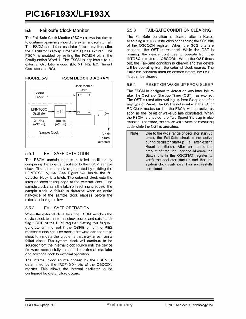
PIC16F193X/LF193X
5.5 Fail-Safe Clock Monitor
The Fail-Safe Clock Monitor (FSCM) allows the deviceto continue operating should the external oscillator fail.The FSCM can detect oscillator failure any time afterthe Oscillator Start-up Timer (OST) has expired. TheFSCM is enabled by setting the FCMEN bit in theConfiguration Word 1. The FSCM is applicable to allexternal Oscillator modes (LP, XT, HS, EC, Timer1Oscillator and RC).
FIGURE 5-9: FSCM BLOCK DIAGRAM
5.5.1 FAIL-SAFE DETECTION
The FSCM module detects a failed oscillator bycomparing the external oscillator to the FSCM sampleclock. The sample clock is generated by dividing theLFINTOSC by 64. See Figure 5-9. Inside the faildetector block is a latch. The external clock sets thelatch on each falling edge of the external clock. Thesample clock clears the latch on each rising edge of thesample clock. A failure is detected when an entirehalf-cycle of the sample clock elapses before theexternal clock goes low.
5.5.2 FAIL-SAFE OPERATION
When the external clock fails, the FSCM switches thedevice clock to an internal clock source and sets the bitflag OSFIF of the PIR2 register. Setting this flag willgenerate an interrupt if the OSFIE bit of the PIE2register is also set. The device firmware can then takesteps to mitigate the problems that may arise from afailed clock. The system clock will continue to besourced from the internal clock source until the devicefirmware successfully restarts the external oscillatorand switches back to external operation.
The internal clock source chosen by the FSCM isdetermined by the IRCF<3:0> bits of the OSCCONregister. This allows the internal oscillator to beconfigured before a failure occurs.
5.5.3 FAIL-SAFE CONDITION CLEARING
The Fail-Safe condition is cleared after a Reset,executing a SLEEP instruction or changing the SCS bitsof the OSCCON register. When the SCS bits arechanged, the OST is restarted. While the OST isrunning, the device continues to operate from theINTOSC selected in OSCCON. When the OST timesout, the Fail-Safe condition is cleared and the devicewill be operating from the external clock source. TheFail-Safe condition must be cleared before the OSFIFflag can be cleared.
5.5.4 RESET OR WAKE-UP FROM SLEEP
The FSCM is designed to detect an oscillator failureafter the Oscillator Start-up Timer (OST) has expired.The OST is used after waking up from Sleep and afterany type of Reset. The OST is not used with the EC orRC Clock modes so that the FSCM will be active assoon as the Reset or wake-up has completed. Whenthe FSCM is enabled, the Two-Speed Start-up is alsoenabled. Therefore, the device will always be executingcode while the OST is operating.
External
LFINTOSC÷ 64
S
R
Q
31 kHz(~32 s)
488 Hz(~2 ms)
Clock MonitorLatch
ClockFailure
Detected
Oscillator
Clock
Q
Sample Clock Note: Due to the wide range of oscillator start-uptimes, the Fail-Safe circuit is not activeduring oscillator start-up (i.e., after exitingReset or Sleep). After an appropriateamount of time, the user should check theStatus bits in the OSCSTAT register toverify the oscillator start-up and that thesystem clock switchover has successfullycompleted.
DS41364D-page 80 Preliminary 2009 Microchip Technology Inc.
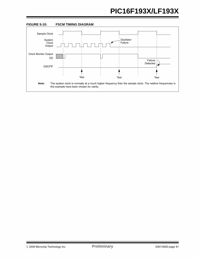
PIC16F193X/LF193X
FIGURE 5-10: FSCM TIMING DIAGRAM
OSCFIF
SystemClock
Output
Sample Clock
FailureDetected
OscillatorFailure
Note: The system clock is normally at a much higher frequency than the sample clock. The relative frequencies inthis example have been chosen for clarity.
(Q)
Test Test Test
Clock Monitor Output
2009 Microchip Technology Inc. Preliminary DS41364D-page 81
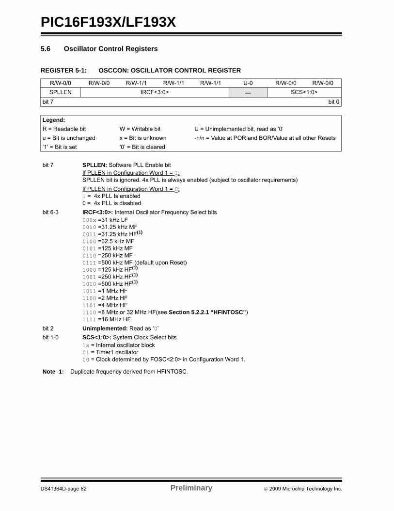
PIC16F193X/LF193X
5.6 Oscillator Control Registers
REGISTER 5-1: OSCCON: OSCILLATOR CONTROL REGISTER
R/W-0/0 R/W-0/0 R/W-1/1 R/W-1/1 R/W-1/1 U-0 R/W-0/0 R/W-0/0
SPLLEN IRCF<3:0> — SCS<1:0>
bit 7 bit 0
Legend:
R = Readable bit W = Writable bit U = Unimplemented bit, read as ‘0’
u = Bit is unchanged x = Bit is unknown -n/n = Value at POR and BOR/Value at all other Resets
‘1’ = Bit is set ‘0’ = Bit is cleared
bit 7 SPLLEN: Software PLL Enable bitIf PLLEN in Configuration Word 1 = 1:SPLLEN bit is ignored. 4x PLL is always enabled (subject to oscillator requirements)
If PLLEN in Configuration Word 1 = 0:1 = 4x PLL Is enabled0 = 4x PLL is disabled
bit 6-3 IRCF<3:0>: Internal Oscillator Frequency Select bits000x =31 kHz LF0010 =31.25 kHz MF0011 =31.25 kHz HF(1)
0100 =62.5 kHz MF0101 =125 kHz MF0110 =250 kHz MF0111 =500 kHz MF (default upon Reset)1000 =125 kHz HF(1)
1001 =250 kHz HF(1)
1010 =500 kHz HF(1)
1011 =1 MHz HF1100 =2 MHz HF1101 =4 MHz HF1110 =8 MHz or 32 MHz HF(see Section 5.2.2.1 “HFINTOSC”)1111 =16 MHz HF
bit 2 Unimplemented: Read as ‘0’
bit 1-0 SCS<1:0>: System Clock Select bits1x = Internal oscillator block01 = Timer1 oscillator00 = Clock determined by FOSC<2:0> in Configuration Word 1.
Note 1: Duplicate frequency derived from HFINTOSC.
DS41364D-page 82 Preliminary 2009 Microchip Technology Inc.
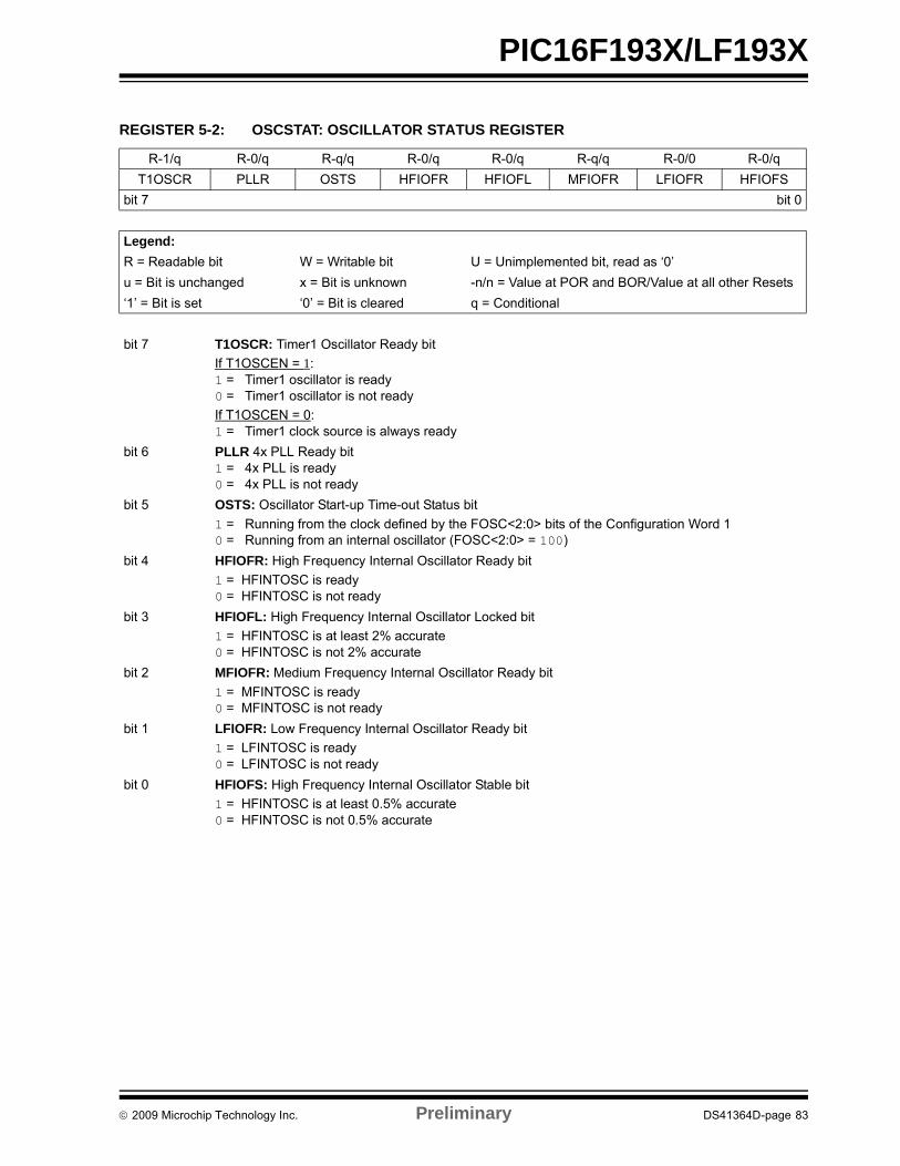
PIC16F193X/LF193X
REGISTER 5-2: OSCSTAT: OSCILLATOR STATUS REGISTER
R-1/q R-0/q R-q/q R-0/q R-0/q R-q/q R-0/0 R-0/q
T1OSCR PLLR OSTS HFIOFR HFIOFL MFIOFR LFIOFR HFIOFS
bit 7 bit 0
Legend:
R = Readable bit W = Writable bit U = Unimplemented bit, read as ‘0’
u = Bit is unchanged x = Bit is unknown -n/n = Value at POR and BOR/Value at all other Resets
‘1’ = Bit is set ‘0’ = Bit is cleared q = Conditional
bit 7 T1OSCR: Timer1 Oscillator Ready bit
If T1OSCEN = 1:1 = Timer1 oscillator is ready0 = Timer1 oscillator is not ready
If T1OSCEN = 0:1 = Timer1 clock source is always ready
bit 6 PLLR 4x PLL Ready bit1 = 4x PLL is ready0 = 4x PLL is not ready
bit 5 OSTS: Oscillator Start-up Time-out Status bit
1 = Running from the clock defined by the FOSC<2:0> bits of the Configuration Word 10 = Running from an internal oscillator (FOSC<2:0> = 100)
bit 4 HFIOFR: High Frequency Internal Oscillator Ready bit
1 = HFINTOSC is ready0 = HFINTOSC is not ready
bit 3 HFIOFL: High Frequency Internal Oscillator Locked bit
1 = HFINTOSC is at least 2% accurate0 = HFINTOSC is not 2% accurate
bit 2 MFIOFR: Medium Frequency Internal Oscillator Ready bit
1 = MFINTOSC is ready 0 = MFINTOSC is not ready
bit 1 LFIOFR: Low Frequency Internal Oscillator Ready bit
1 = LFINTOSC is ready0 = LFINTOSC is not ready
bit 0 HFIOFS: High Frequency Internal Oscillator Stable bit
1 = HFINTOSC is at least 0.5% accurate0 = HFINTOSC is not 0.5% accurate
2009 Microchip Technology Inc. Preliminary DS41364D-page 83

PIC16F193X/LF193X
TABLE 5-2: SUMMARY OF REGISTERS ASSOCIATED WITH CLOCK SOURCES
TABLE 5-3: SUMMARY OF CONFIGURATION WORD WITH CLOCK SOURCES
REGISTER 5-3: OSCTUNE: OSCILLATOR TUNING REGISTER
U-0 U-0 R/W-0/0 R/W-0/0 R/W-0/0 R/W-0/0 R/W-0/0 R/W-0/0
— — TUN<5:0>
bit 7 bit 0
Legend:
R = Readable bit W = Writable bit U = Unimplemented bit, read as ‘0’
u = Bit is unchanged x = Bit is unknown -n/n = Value at POR and BOR/Value at all other Resets
‘1’ = Bit is set ‘0’ = Bit is cleared
bit 7-6 Unimplemented: Read as ‘0’
bit 5-0 TUN<4:0>: Frequency Tuning bits011111 = Maximum frequency011110 = •••000001 = 000000 = Oscillator module is running at the factory-calibrated frequency.111111 = •••100000 = Minimum frequency
Name Bit 7 Bit 6 Bit 5 Bit 4 Bit 3 Bit 2 Bit 1 Bit 0Register on Page
OSCCON SPLLEN IRCF<3:0> — SCS<1:0> 82
OSCSTAT T1OSCR PLLR OSTS HFIOFR HFIOFL MFIOFR LFIOFR HFIOFS 83
OSCTUNE — — TUN<5:0> 84
PIE2 OSFIE C2IE C1IE EEIE BCLIE LCDIE — CCP2IE(1) 101
PIR2 OSFIF C2IF C1IF EEIF BCLIF LCDIF — CCP2IF(1) 104
T1CON TMR1CS<1:0> T1CKPS<1:0> T1OSCEN T1SYNC — TMR1ON 201
Legend: — = unimplemented location, read as ‘0’. Shaded cells are not used by clock sources.Note 1: PIC16F1934 only.
Name Bits Bit -/7 Bit -/6 Bit 13/5 Bit 12/4 Bit 11/3 Bit 10/2 Bit 9/1 Bit 8/0Register on Page
CONFIG113:8 — — FCMEN IESO CLKOUTEN BOREN<1:0> CPD
647:0 CP MCLRE PWRTE WDTE<1:0> FOSC<2:0>
CONFIG213:8 — — LVP DEBUG — BORV STVREN PLLEN
667:0 — — VCAPEN<1:0>(1) — — WRT<1:0>
Legend: — = unimplemented location, read as ‘0’. Shaded cells are not used by clock sources.Note 1: PIC16F193X only.
DS41364D-page 84 Preliminary 2009 Microchip Technology Inc.
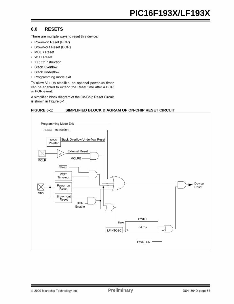
PIC16F193X/LF193X
6.0 RESETS
There are multiple ways to reset this device:
• Power-on Reset (POR)
• Brown-out Reset (BOR)
• MCLR Reset
• WDT Reset
• RESET instruction
• Stack Overflow
• Stack Underflow
• Programming mode exit
To allow VDD to stabilize, an optional power-up timercan be enabled to extend the Reset time after a BORor POR event.
A simplified block diagram of the On-Chip Reset Circuitis shown in Figure 6-1.
FIGURE 6-1: SIMPLIFIED BLOCK DIAGRAM OF ON-CHIP RESET CIRCUIT
External Reset
MCLR
VDD
WDTTime-out
Power-onReset
LFINTOSC
PWRT
64 ms
PWRTEN
Brown-outReset
BOR
RESET Instruction
StackPointer
Stack Overflow/Underflow Reset
Sleep
MCLRE
Enable
DeviceReset
Zero
Programming Mode Exit
2009 Microchip Technology Inc. Preliminary DS41364D-page 85
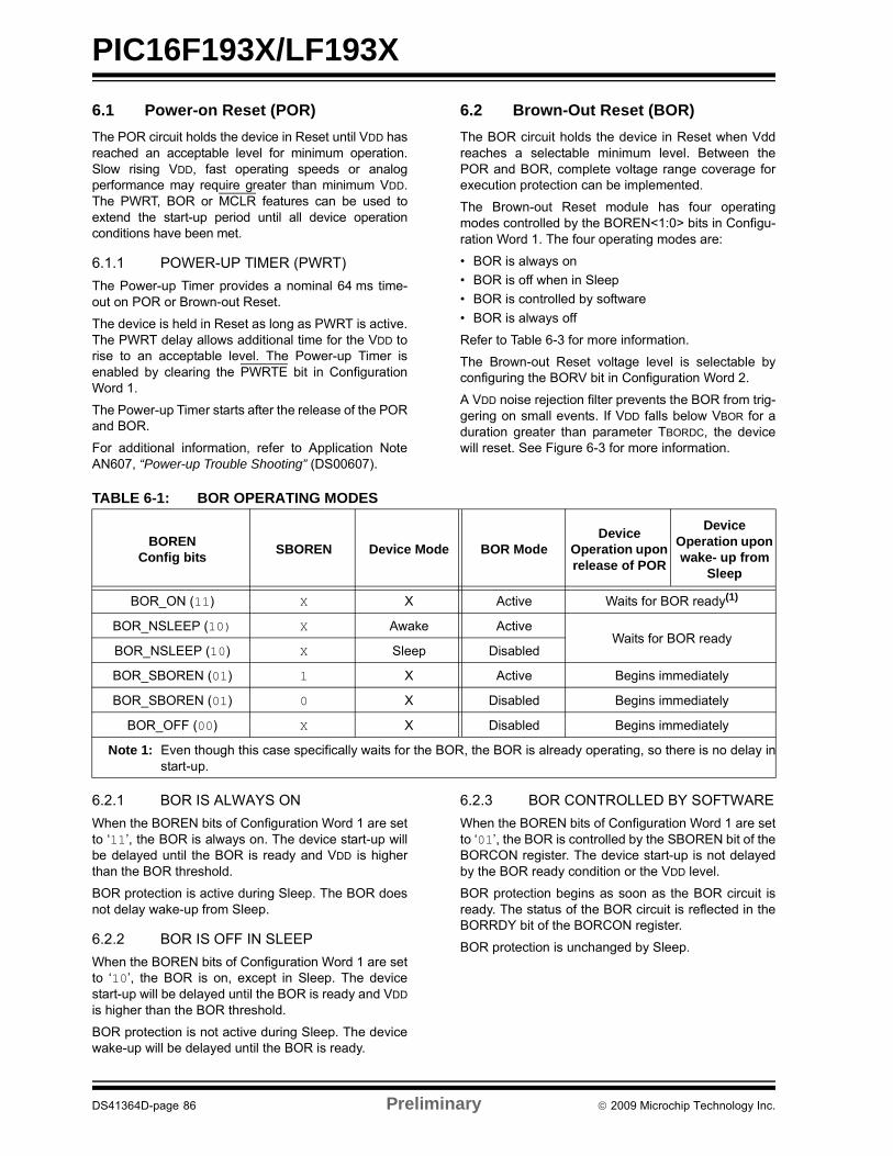
PIC16F193X/LF193X
6.1 Power-on Reset (POR)
The POR circuit holds the device in Reset until VDD hasreached an acceptable level for minimum operation.Slow rising VDD, fast operating speeds or analogperformance may require greater than minimum VDD.The PWRT, BOR or MCLR features can be used toextend the start-up period until all device operationconditions have been met.
6.1.1 POWER-UP TIMER (PWRT)
The Power-up Timer provides a nominal 64 ms time-out on POR or Brown-out Reset.
The device is held in Reset as long as PWRT is active.The PWRT delay allows additional time for the VDD torise to an acceptable level. The Power-up Timer isenabled by clearing the PWRTE bit in ConfigurationWord 1.
The Power-up Timer starts after the release of the PORand BOR.
For additional information, refer to Application NoteAN607, “Power-up Trouble Shooting” (DS00607).
6.2 Brown-Out Reset (BOR)
The BOR circuit holds the device in Reset when Vddreaches a selectable minimum level. Between thePOR and BOR, complete voltage range coverage forexecution protection can be implemented.
The Brown-out Reset module has four operatingmodes controlled by the BOREN<1:0> bits in Configu-ration Word 1. The four operating modes are:
• BOR is always on
• BOR is off when in Sleep
• BOR is controlled by software
• BOR is always off
Refer to Table 6-3 for more information.
The Brown-out Reset voltage level is selectable byconfiguring the BORV bit in Configuration Word 2.
A VDD noise rejection filter prevents the BOR from trig-gering on small events. If VDD falls below VBOR for aduration greater than parameter TBORDC, the devicewill reset. See Figure 6-3 for more information.
TABLE 6-1: BOR OPERATING MODES
6.2.1 BOR IS ALWAYS ON
When the BOREN bits of Configuration Word 1 are setto ‘11’, the BOR is always on. The device start-up willbe delayed until the BOR is ready and VDD is higherthan the BOR threshold.
BOR protection is active during Sleep. The BOR doesnot delay wake-up from Sleep.
6.2.2 BOR IS OFF IN SLEEP
When the BOREN bits of Configuration Word 1 are setto ‘10’, the BOR is on, except in Sleep. The devicestart-up will be delayed until the BOR is ready and VDD
is higher than the BOR threshold.
BOR protection is not active during Sleep. The devicewake-up will be delayed until the BOR is ready.
6.2.3 BOR CONTROLLED BY SOFTWARE
When the BOREN bits of Configuration Word 1 are setto ‘01’, the BOR is controlled by the SBOREN bit of theBORCON register. The device start-up is not delayedby the BOR ready condition or the VDD level.
BOR protection begins as soon as the BOR circuit isready. The status of the BOR circuit is reflected in theBORRDY bit of the BORCON register.
BOR protection is unchanged by Sleep.
BORENConfig bits
SBOREN Device Mode BOR ModeDevice
Operation upon release of POR
Device Operation upon wake- up from
Sleep
BOR_ON (11) X X Active Waits for BOR ready(1)
BOR_NSLEEP (10) X Awake ActiveWaits for BOR ready
BOR_NSLEEP (10) X Sleep Disabled
BOR_SBOREN (01) 1 X Active Begins immediately
BOR_SBOREN (01) 0 X Disabled Begins immediately
BOR_OFF (00) X X Disabled Begins immediately
Note 1: Even though this case specifically waits for the BOR, the BOR is already operating, so there is no delay instart-up.
DS41364D-page 86 Preliminary 2009 Microchip Technology Inc.

PIC16F193X/LF193X
FIGURE 6-2: BROWN-OUT READY
FIGURE 6-3: BROWN-OUT SITUATIONS
REGISTER 6-1: BORCON: BROWN-OUT RESET CONTROL REGISTER
R/W-1/u U-0 U-0 U-0 U-0 U-0 U-0 R-q/u
SBOREN — — — — — — BORRDY
bit 7 bit 0
Legend:
R = Readable bit W = Writable bit U = Unimplemented bit, read as ‘0’
u = Bit is unchanged x = Bit is unknown -n/n = Value at POR and BOR/Value at all other Resets
‘1’ = Bit is set ‘0’ = Bit is cleared q = Value depends on condition
bit 7 SBOREN: Software Brown-out Reset Enable bitIf BOREN <1:0> in Configuration Word 1 01:SBOREN is read/write, but has no effect on the BOR.If BOREN <1:0> in Configuration Word 1 = 01:1 = BOR Enabled0 = BOR Disabled
bit 6-1 Unimplemented: Read as ‘0’
bit 0 BORRDY: Brown-out Reset Circuit Ready Status bit1 = The Brown-out Reset circuit is active0 = The Brown-out Reset circuit is inactive
TBORRDY
SBOREN
BORRDY BOR Protection Active
TPWRT(1)
VBOR VDD
InternalReset
VBOR VDD
InternalReset TPWRT(1)< TPWRT
TPWRT(1)
VBOR VDD
InternalReset
Note 1: TPWRT delay only if PWRTE bit is programmed to ‘0’.
2009 Microchip Technology Inc. Preliminary DS41364D-page 87
PIC16F193X/LF193X
6.3 MCLR
The MCLR is an optional external input that can resetthe device. The MCLR function is controlled by theMCLRE bit of Configuration Word 1 and the LVP bit ofConfiguration Word 2 (Table 6-2).
6.3.1 MCLR ENABLED
When MCLR is enabled and the pin is held low, thedevice is held in Reset. The MCLR pin is connected toVDD through an internal weak pull-up.
The device has a noise filter in the MCLR Reset path.The filter will detect and ignore small pulses.
6.3.2 MCLR DISABLED
When MCLR is disabled, the pin functions as a generalpurpose input and the internal weak pull-up is undersoftware control. See Section 12.6 “PORTERegisters” for more information.
6.4 Watchdog Timer (WDT) Reset
The Watchdog Timer generates a Reset if the firmwaredoes not issue a CLRWDT instruction within the time-outperiod. The TO and PD bits in the STATUS register arechanged to indicate the WDT Reset. See Section 10.0“Watchdog Timer” for more information.
6.5 RESET Instruction
A RESET instruction will cause a device Reset. The RIbit in the PCON register will be set to ‘0’. See Table 6-4for default conditions after a RESET instruction hasoccurred.
6.6 Stack Overflow/Underflow Reset
The device can reset when the Stack Overflows orUnderflows. The STKOVF or STKUNF bits of the PCONregister indicate the Reset condition. These Resets areenabled by setting the STVREN bit in Configuration Word2. See Section 3.4.2 “Overflow/Underflow Reset” formore information.
6.7 Programming Mode Exit
Upon exit of Programming mode, the device willbehave as if a POR had just occurred.
6.8 Power-Up Timer
The Power-up Timer optionally delays device executionafter a BOR or POR event. This timer is typically used toallow VDD to stabilize before allowing the device to startrunning.
The Power-up Timer is controlled by the PWRTE bit ofConfiguration Word 1.
6.9 Start-up Sequence
Upon the release of a POR or BOR, the following mustoccur before the device will begin executing:
1. Power-up Timer runs to completion (if enabled).
2. Oscillator start-up timer runs to completion (ifrequired for oscillator source).
3. MCLR must be released (if enabled).
The total time-out will vary based on oscillator configu-ration and Power-up Timer configuration. SeeSection 5.0 “Oscillator Module (With Fail-SafeClock Monitor)” for more information.
The Power-up Timer and oscillator start-up timer runindependently of MCLR Reset. If MCLR is kept lowlong enough, the Power-up Timer and oscillator start-up timer will expire. Upon bringing MCLR high, thedevice will begin execution immediately (see Figure 6-4). This is useful for testing purposes or to synchronizemore than one device operating in parallel.
TABLE 6-2: MCLR CONFIGURATION
MCLRE LVP MCLR
0 0 Disabled
1 0 Enabled
x 1 Enabled
Note: A Reset does not drive the MCLR pin low.
DS41364D-page 88 Preliminary 2009 Microchip Technology Inc.
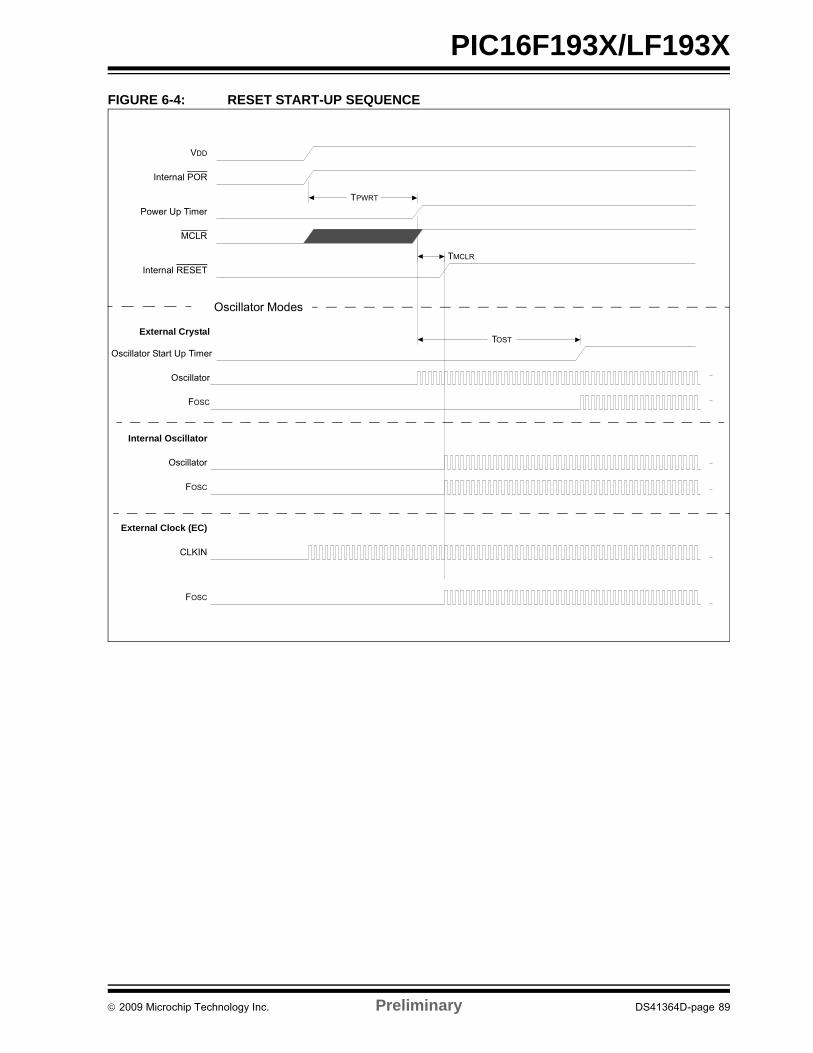
PIC16F193X/LF193X
FIGURE 6-4: RESET START-UP SEQUENCE
TOST
TMCLR
TPWRT
VDD
Internal POR
Power Up Timer
MCLR
Internal RESET
Oscillator Modes
Oscillator Start Up Timer
Oscillator
FOSC
Internal Oscillator
Oscillator
FOSC
External Clock (EC)
CLKIN
FOSC
External Crystal
2009 Microchip Technology Inc. Preliminary DS41364D-page 89

PIC16F193X/LF193X
6.10 Determining the Cause of a Reset
Upon any Reset, multiple bits in the STATUS andPCON register are updated to indicate the cause of theReset. Table 6-3 and Table 6-4 show the Reset condi-tions of these registers.
TABLE 6-3: RESET STATUS BITS AND THEIR SIGNIFICANCE
TABLE 6-4: RESET CONDITION FOR SPECIAL REGISTERS(2)
STKOVF STKUNF RMCLR RI POR BOR TO PD Condition
0 0 1 1 0 x 1 1 Power-on Reset
0 0 1 1 0 x 0 x Illegal, TO is set on POR
0 0 1 1 0 x x 0 Illegal, PD is set on POR
0 0 1 1 u 0 1 1 Brown-out Reset
u u u u u u 0 u WDT Reset
u u u u u u 0 0 WDT Wake-up from Sleep
u u u u u u 1 0 Interrupt Wake-up from Sleep
u u 0 u u u u u MCLR Reset during normal operation
u u 0 u u u 1 0 MCLR Reset during Sleep
u u u 0 u u u u RESET Instruction Executed
1 u u u u u u u Stack Overflow Reset (STVREN = 1)
u 1 u u u u u u Stack Underflow Reset (STVREN = 1)
ConditionProgramCounter
STATUSRegister
PCONRegister
Power-on Reset 0000h ---1 1000 00-- 110x
MCLR Reset during normal operation 0000h ---u uuuu uu-- 0uuu
MCLR Reset during Sleep 0000h ---1 0uuu uu-- 0uuu
WDT Reset 0000h ---0 uuuu uu-- uuuu
WDT Wake-up from Sleep PC + 1 ---0 0uuu uu-- uuuu
Brown-out Reset 0000h ---1 1uuu 00-- 11u0
Interrupt Wake-up from Sleep PC + 1(1) ---1 0uuu uu-- uuuu
RESET Instruction Executed 0000h ---u uuuu uu-- u0uu
Stack Overflow Reset (STVREN = 1) 0000h ---u uuuu 1u-- uuuu
Stack Underflow Reset (STVREN = 1) 0000h ---u uuuu u1-- uuuu
Legend: u = unchanged, x = unknown, - = unimplemented bit, reads as ‘0’.Note 1: When the wake-up is due to an interrupt and Global Enable bit (GIE) is set, the return address is pushed on
the stack and PC is loaded with the interrupt vector (0004h) after execution of PC + 1.2: If a Status bit is not implemented, that bit will be read as ‘0’.
DS41364D-page 90 Preliminary 2009 Microchip Technology Inc.
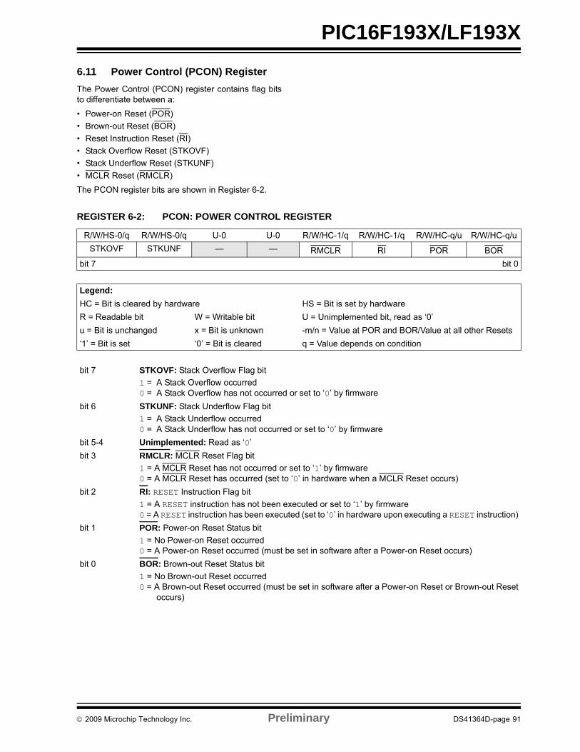
PIC16F193X/LF193X
6.11 Power Control (PCON) Register
The Power Control (PCON) register contains flag bitsto differentiate between a:
• Power-on Reset (POR)
• Brown-out Reset (BOR)
• Reset Instruction Reset (RI)
• Stack Overflow Reset (STKOVF)
• Stack Underflow Reset (STKUNF)
• MCLR Reset (RMCLR)
The PCON register bits are shown in Register 6-2.
REGISTER 6-2: PCON: POWER CONTROL REGISTER
R/W/HS-0/q R/W/HS-0/q U-0 U-0 R/W/HC-1/q R/W/HC-1/q R/W/HC-q/u R/W/HC-q/u
STKOVF STKUNF — — RMCLR RI POR BOR
bit 7 bit 0
Legend:
HC = Bit is cleared by hardware HS = Bit is set by hardware
R = Readable bit W = Writable bit U = Unimplemented bit, read as ‘0’
u = Bit is unchanged x = Bit is unknown -m/n = Value at POR and BOR/Value at all other Resets
‘1’ = Bit is set ‘0’ = Bit is cleared q = Value depends on condition
bit 7 STKOVF: Stack Overflow Flag bit
1 = A Stack Overflow occurred0 = A Stack Overflow has not occurred or set to ‘0’ by firmware
bit 6 STKUNF: Stack Underflow Flag bit
1 = A Stack Underflow occurred0 = A Stack Underflow has not occurred or set to ‘0’ by firmware
bit 5-4 Unimplemented: Read as ‘0’
bit 3 RMCLR: MCLR Reset Flag bit
1 = A MCLR Reset has not occurred or set to ‘1’ by firmware0 = A MCLR Reset has occurred (set to ‘0’ in hardware when a MCLR Reset occurs)
bit 2 RI: RESET Instruction Flag bit
1 = A RESET instruction has not been executed or set to ‘1’ by firmware0 = A RESET instruction has been executed (set to ‘0’ in hardware upon executing a RESET instruction)
bit 1 POR: Power-on Reset Status bit
1 = No Power-on Reset occurred0 = A Power-on Reset occurred (must be set in software after a Power-on Reset occurs)
bit 0 BOR: Brown-out Reset Status bit
1 = No Brown-out Reset occurred0 = A Brown-out Reset occurred (must be set in software after a Power-on Reset or Brown-out Reset
occurs)
2009 Microchip Technology Inc. Preliminary DS41364D-page 91
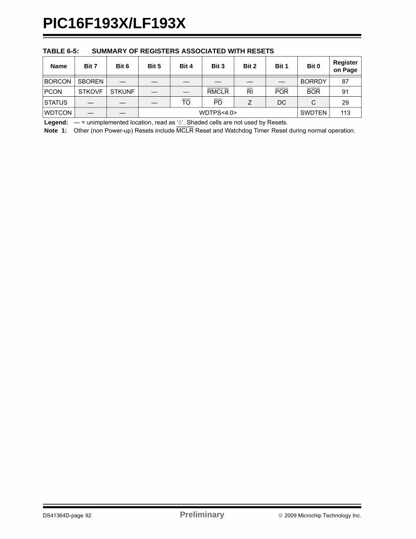
PIC16F193X/LF193X
TABLE 6-5: SUMMARY OF REGISTERS ASSOCIATED WITH RESETS
Name Bit 7 Bit 6 Bit 5 Bit 4 Bit 3 Bit 2 Bit 1 Bit 0Register on Page
BORCON SBOREN — — — — — — BORRDY 87
PCON STKOVF STKUNF — — RMCLR RI POR BOR 91
STATUS — — — TO PD Z DC C 29
WDTCON — — WDTPS<4:0> SWDTEN 113
Legend: — = unimplemented location, read as ‘0’. Shaded cells are not used by Resets.Note 1: Other (non Power-up) Resets include MCLR Reset and Watchdog Timer Reset during normal operation.
DS41364D-page 92 Preliminary 2009 Microchip Technology Inc.
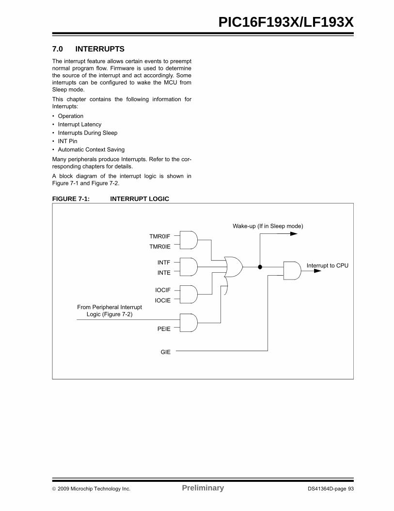
PIC16F193X/LF193X
7.0 INTERRUPTS
The interrupt feature allows certain events to preemptnormal program flow. Firmware is used to determinethe source of the interrupt and act accordingly. Someinterrupts can be configured to wake the MCU fromSleep mode.
This chapter contains the following information forInterrupts:
• Operation
• Interrupt Latency
• Interrupts During Sleep
• INT Pin
• Automatic Context Saving
Many peripherals produce Interrupts. Refer to the cor-responding chapters for details.
A block diagram of the interrupt logic is shown inFigure 7-1 and Figure 7-2.
FIGURE 7-1: INTERRUPT LOGIC
TMR0IF
TMR0IE
INTF
INTE
IOCIF
IOCIE
GIE
PEIE
Wake-up (If in Sleep mode)
Interrupt to CPU
From Peripheral Interrupt Logic (Figure 7-2)
2009 Microchip Technology Inc. Preliminary DS41364D-page 93

PIC16F193X/LF193X
FIGURE 7-2: PERIPHERAL INTERRUPT LOGIC
TMR1GIFTMR1GIE
ADIFADIE
RCIFRCIE
TXIFTXIE
SSPIFSSPIE
OSFIFOSFIE
C2IFC2IE
C1IFC1IEEEIFEEIE
BCLIFBCLIE
LCDIFLCDIE
TMR1IFTMR1IE
TMR6IFTMR6IE
CCP1IFCCP1IE
CCP5IFCCP5IE
To Interrupt Logic(Figure 7-1)
DS41364D-page 94 Preliminary 2009 Microchip Technology Inc.

PIC16F193X/LF193X
7.1 Operation
Interrupts are disabled upon any device Reset. Theyare enabled by setting the following bits:
• GIE bit of the INTCON register
• Interrupt Enable bit(s) for the specific interrupt event(s)
• PEIE bit of the INTCON register (if the Interrupt Enable bit of the interrupt event is contained in the PIE1, PIE2 and PIE3 registers)
The INTCON, PIR1, PIR2 and PIR3 registers recordindividual interrupts via interrupt flag bits. Interrupt flagbits will be set, regardless of the status of the GIE, PEIEand individual interrupt enable bits.
The following events happen when an interrupt eventoccurs while the GIE bit is set:
• Current prefetched instruction is flushed
• GIE bit is cleared
• Current Program Counter (PC) is pushed onto the stack
• Critical registers are automatically saved to the shadow registers (See Section 7.5 “Automatic Context Saving”)
• PC is loaded with the interrupt vector 0004h
The firmware within the Interrupt Service Routine (ISR)should determine the source of the interrupt by pollingthe interrupt flag bits. The interrupt flag bits must becleared before exiting the ISR to avoid repeatedinterrupts. Because the GIE bit is cleared, any interruptthat occurs while executing the ISR will be recordedthrough its interrupt flag, but will not cause theprocessor to redirect to the interrupt vector.
The RETFIE instruction exits the ISR by popping theprevious address from the stack, restoring the savedcontext from the shadow registers and setting the GIEbit.
For additional information on a specific interrupt’soperation, refer to its peripheral chapter.
7.2 Interrupt Latency
Interrupt latency is defined as the time from when theinterrupt event occurs to the time code execution at theinterrupt vector begins. The latency for synchronousinterrupts is 3 or 4 instruction cycles. For asynchronousinterrupts, the latency is 3 to 5 instruction cycles,depending on when the interrupt occurs. See Figure 7-3and Figure 7-4 for more details.
Note 1: Individual interrupt flag bits are set,regardless of the state of any otherenable bits.
2: All interrupts will be ignored while the GIEbit is cleared. Any interrupt occurringwhile the GIE bit is clear will be servicedwhen the GIE bit is set again.
2009 Microchip Technology Inc. Preliminary DS41364D-page 95

PIC16F193X/LF193X
FIGURE 7-3: INTERRUPT LATENCY
Q1 Q2 Q3 Q4 Q1 Q2 Q3 Q4 Q1 Q2 Q3 Q4 Q1 Q2 Q3 Q4 Q1 Q2 Q3 Q4 Q1 Q2 Q3 Q4
OSC1
CLKOUT
PC 0004h 0005hPC
Inst(0004h)NOP
GIE
Q1 Q2 Q3 Q4Q1 Q2 Q3 Q4
1 Cycle Instruction at PC
PC
Inst(0004h)NOP2 Cycle Instruction at PC
FSR ADDR PC+1 PC+2 0004h 0005hPC
Inst(0004h)NOP
GIE
PCPC-1
3 Cycle Instruction at PC
Execute
Interrupt
Inst(PC)
Interrupt Sampled during Q1
Inst(PC)
PC-1 PC+1
NOP
PCNew PC/
PC+10005hPC-1
PC+1/FSR ADDR
0004h
NOP
Interrupt
GIE
Interrupt
INST(PC) NOPNOP
FSR ADDR PC+1 PC+2 0004h 0005hPC
Inst(0004h)NOP
GIE
PCPC-1
3 Cycle Instruction at PC
Interrupt
INST(PC) NOPNOP NOP
Inst(0005h)
Execute
Execute
Execute
DS41364D-page 96 Preliminary 2009 Microchip Technology Inc.
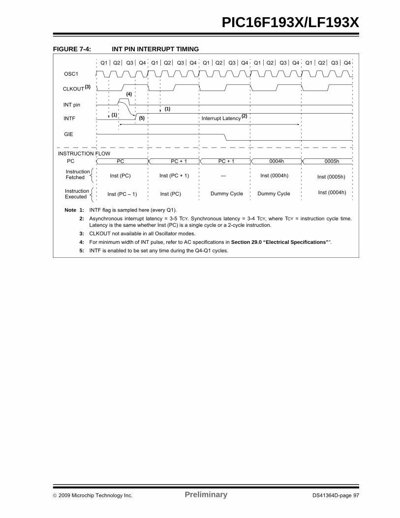
PIC16F193X/LF193X
FIGURE 7-4: INT PIN INTERRUPT TIMING
Q2Q1 Q3 Q4 Q2Q1 Q3 Q4 Q2Q1 Q3 Q4 Q2Q1 Q3 Q4 Q2Q1 Q3 Q4
OSC1
CLKOUT
INT pin
INTF
GIE
INSTRUCTION FLOW
PC
InstructionFetched
InstructionExecuted
Interrupt Latency
PC PC + 1 PC + 1 0004h 0005h
Inst (0004h) Inst (0005h)
Dummy Cycle
Inst (PC) Inst (PC + 1)
Inst (PC – 1) Inst (0004h)Dummy CycleInst (PC)
—
Note 1: INTF flag is sampled here (every Q1).
2: Asynchronous interrupt latency = 3-5 TCY. Synchronous latency = 3-4 TCY, where TCY = instruction cycle time.Latency is the same whether Inst (PC) is a single cycle or a 2-cycle instruction.
3: CLKOUT not available in all Oscillator modes.
4: For minimum width of INT pulse, refer to AC specifications in Section 29.0 “Electrical Specifications””.
5: INTF is enabled to be set any time during the Q4-Q1 cycles.
(1)
(2)
(3)
(4)
(5)(1)
2009 Microchip Technology Inc. Preliminary DS41364D-page 97

PIC16F193X/LF193X
7.3 Interrupts During Sleep
Some interrupts can be used to wake from Sleep. Towake from Sleep, the peripheral must be able tooperate without the system clock. The interrupt sourcemust have the appropriate Interrupt Enable bit(s) setprior to entering Sleep.
On waking from Sleep, if the GIE bit is also set, theprocessor will branch to the interrupt vector. Otherwise,the processor will continue executing instructions afterthe SLEEP instruction. The instruction directly after theSLEEP instruction will always be executed beforebranching to the ISR. Refer to the Section 9.0 “Power-Down Mode (Sleep)” for more details.
7.4 INT Pin
The INT pin can be used to generate an asynchronousedge-triggered interrupt. This interrupt is enabled bysetting the INTE bit of the INTCON register. TheINTEDG bit of the OPTION register determines on whichedge the interrupt will occur. When the INTEDG bit isset, the rising edge will cause the interrupt. When theINTEDG bit is clear, the falling edge will cause theinterrupt. The INTF bit of the INTCON register will be setwhen a valid edge appears on the INT pin. If the GIE andINTE bits are also set, the processor will redirectprogram execution to the interrupt vector.
7.5 Automatic Context Saving
Upon entering an interrupt, the return PC address issaved on the stack. Additionally, the following registersare automatically saved in the Shadow registers:
• W register
• STATUS register (except for TO and PD)
• BSR register
• FSR registers
• PCLATH register
Upon exiting the Interrupt Service Routine, these regis-ters are automatically restored. Any modifications tothese registers during the ISR will be lost. If modifica-tions to any of these registers are desired, the corre-sponding Shadow register should be modified and thevalue will be restored when exiting the ISR. TheShadow registers are available in Bank 31 and arereadable and writable. Depending on the user’s appli-cation, other registers may also need to be saved.
DS41364D-page 98 Preliminary 2009 Microchip Technology Inc.
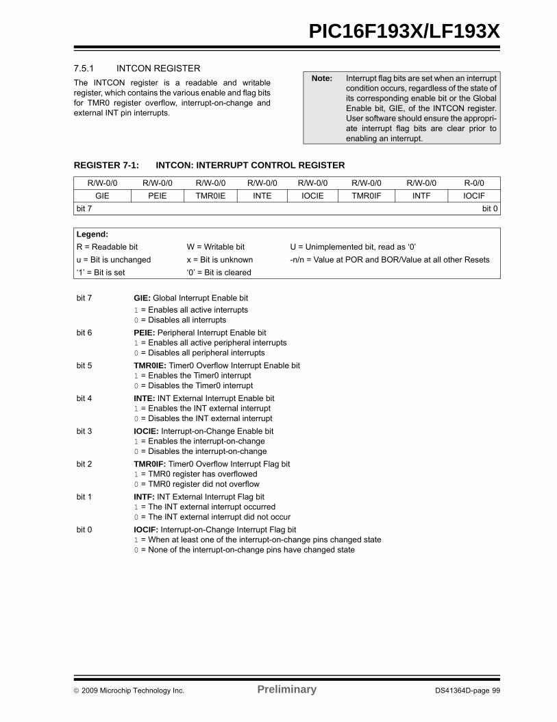
PIC16F193X/LF193X
7.5.1 INTCON REGISTER
The INTCON register is a readable and writableregister, which contains the various enable and flag bitsfor TMR0 register overflow, interrupt-on-change andexternal INT pin interrupts.
Note: Interrupt flag bits are set when an interruptcondition occurs, regardless of the state ofits corresponding enable bit or the GlobalEnable bit, GIE, of the INTCON register.User software should ensure the appropri-ate interrupt flag bits are clear prior toenabling an interrupt.
REGISTER 7-1: INTCON: INTERRUPT CONTROL REGISTER
R/W-0/0 R/W-0/0 R/W-0/0 R/W-0/0 R/W-0/0 R/W-0/0 R/W-0/0 R-0/0
GIE PEIE TMR0IE INTE IOCIE TMR0IF INTF IOCIF
bit 7 bit 0
Legend:
R = Readable bit W = Writable bit U = Unimplemented bit, read as ‘0’
u = Bit is unchanged x = Bit is unknown -n/n = Value at POR and BOR/Value at all other Resets
‘1’ = Bit is set ‘0’ = Bit is cleared
bit 7 GIE: Global Interrupt Enable bit
1 = Enables all active interrupts0 = Disables all interrupts
bit 6 PEIE: Peripheral Interrupt Enable bit1 = Enables all active peripheral interrupts0 = Disables all peripheral interrupts
bit 5 TMR0IE: Timer0 Overflow Interrupt Enable bit1 = Enables the Timer0 interrupt0 = Disables the Timer0 interrupt
bit 4 INTE: INT External Interrupt Enable bit1 = Enables the INT external interrupt0 = Disables the INT external interrupt
bit 3 IOCIE: Interrupt-on-Change Enable bit1 = Enables the interrupt-on-change0 = Disables the interrupt-on-change
bit 2 TMR0IF: Timer0 Overflow Interrupt Flag bit1 = TMR0 register has overflowed0 = TMR0 register did not overflow
bit 1 INTF: INT External Interrupt Flag bit1 = The INT external interrupt occurred0 = The INT external interrupt did not occur
bit 0 IOCIF: Interrupt-on-Change Interrupt Flag bit1 = When at least one of the interrupt-on-change pins changed state0 = None of the interrupt-on-change pins have changed state
2009 Microchip Technology Inc. Preliminary DS41364D-page 99
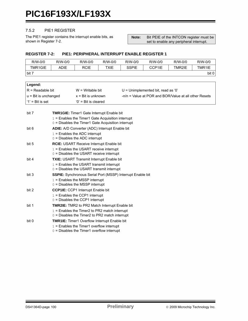
PIC16F193X/LF193X
7.5.2 PIE1 REGISTER
The PIE1 register contains the interrupt enable bits, asshown in Register 7-2.
Note: Bit PEIE of the INTCON register must beset to enable any peripheral interrupt.
REGISTER 7-2: PIE1: PERIPHERAL INTERRUPT ENABLE REGISTER 1
R/W-0/0 R/W-0/0 R/W-0/0 R/W-0/0 R/W-0/0 R/W-0/0 R/W-0/0 R/W-0/0
TMR1GIE ADIE RCIE TXIE SSPIE CCP1IE TMR2IE TMR1IE
bit 7 bit 0
Legend:
R = Readable bit W = Writable bit U = Unimplemented bit, read as ‘0’
u = Bit is unchanged x = Bit is unknown -n/n = Value at POR and BOR/Value at all other Resets
‘1’ = Bit is set ‘0’ = Bit is cleared
bit 7 TMR1GIE: Timer1 Gate Interrupt Enable bit
1 = Enables the Timer1 Gate Acquisition interrupt0 = Disables the Timer1 Gate Acquisition interrupt
bit 6 ADIE: A/D Converter (ADC) Interrupt Enable bit
1 = Enables the ADC interrupt0 = Disables the ADC interrupt
bit 5 RCIE: USART Receive Interrupt Enable bit
1 = Enables the USART receive interrupt0 = Disables the USART receive interrupt
bit 4 TXIE: USART Transmit Interrupt Enable bit
1 = Enables the USART transmit interrupt0 = Disables the USART transmit interrupt
bit 3 SSPIE: Synchronous Serial Port (MSSP) Interrupt Enable bit
1 = Enables the MSSP interrupt0 = Disables the MSSP interrupt
bit 2 CCP1IE: CCP1 Interrupt Enable bit
1 = Enables the CCP1 interrupt0 = Disables the CCP1 interrupt
bit 1 TMR2IE: TMR2 to PR2 Match Interrupt Enable bit
1 = Enables the Timer2 to PR2 match interrupt0 = Disables the Timer2 to PR2 match interrupt
bit 0 TMR1IE: Timer1 Overflow Interrupt Enable bit
1 = Enables the Timer1 overflow interrupt0 = Disables the Timer1 overflow interrupt
DS41364D-page 100 Preliminary 2009 Microchip Technology Inc.
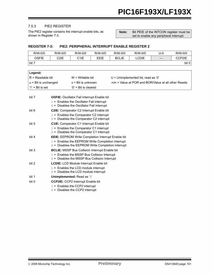
PIC16F193X/LF193X
7.5.3 PIE2 REGISTER
The PIE2 register contains the interrupt enable bits, asshown in Register 7-3.
Note: Bit PEIE of the INTCON register must beset to enable any peripheral interrupt.
REGISTER 7-3: PIE2: PERIPHERAL INTERRUPT ENABLE REGISTER 2
R/W-0/0 R/W-0/0 R/W-0/0 R/W-0/0 R/W-0/0 R/W-0/0 U-0 R/W-0/0
OSFIE C2IE C1IE EEIE BCLIE LCDIE — CCP2IE
bit 7 bit 0
Legend:
R = Readable bit W = Writable bit U = Unimplemented bit, read as ‘0’
u = Bit is unchanged x = Bit is unknown -n/n = Value at POR and BOR/Value at all other Resets
‘1’ = Bit is set ‘0’ = Bit is cleared
bit 7 OSFIE: Oscillator Fail Interrupt Enable bit
1 = Enables the Oscillator Fail interrupt0 = Disables the Oscillator Fail interrupt
bit 6 C2IE: Comparator C2 Interrupt Enable bit
1 = Enables the Comparator C2 interrupt0 = Disables the Comparator C2 interrupt
bit 5 C1IE: Comparator C1 Interrupt Enable bit
1 = Enables the Comparator C1 interrupt0 = Disables the Comparator C1 interrupt
bit 4 EEIE: EEPROM Write Completion Interrupt Enable bit
1 = Enables the EEPROM Write Completion interrupt0 = Disables the EEPROM Write Completion interrupt
bit 3 BCLIE: MSSP Bus Collision Interrupt Enable bit
1 = Enables the MSSP Bus Collision Interrupt0 = Disables the MSSP Bus Collision Interrupt
bit 2 LCDIE: LCD Module Interrupt Enable bit
1 = Enables the LCD module interrupt0 = Disables the LCD module interrupt
bit 1 Unimplemented: Read as ‘0’
bit 0 CCP2IE: CCP2 Interrupt Enable bit
1 = Enables the CCP2 interrupt0 = Disables the CCP2 interrupt
2009 Microchip Technology Inc. Preliminary DS41364D-page 101
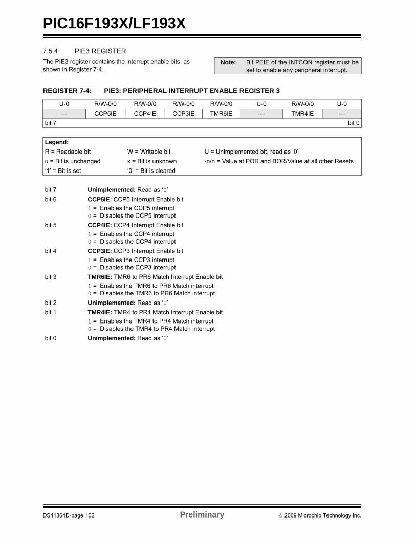
PIC16F193X/LF193X
7.5.4 PIE3 REGISTER
The PIE3 register contains the interrupt enable bits, asshown in Register 7-4.
Note: Bit PEIE of the INTCON register must beset to enable any peripheral interrupt.
REGISTER 7-4: PIE3: PERIPHERAL INTERRUPT ENABLE REGISTER 3
U-0 R/W-0/0 R/W-0/0 R/W-0/0 R/W-0/0 U-0 R/W-0/0 U-0
— CCP5IE CCP4IE CCP3IE TMR6IE — TMR4IE —
bit 7 bit 0
Legend:
R = Readable bit W = Writable bit U = Unimplemented bit, read as ‘0’
u = Bit is unchanged x = Bit is unknown -n/n = Value at POR and BOR/Value at all other Resets
‘1’ = Bit is set ‘0’ = Bit is cleared
bit 7 Unimplemented: Read as ‘0’
bit 6 CCP5IE: CCP5 Interrupt Enable bit
1 = Enables the CCP5 interrupt0 = Disables the CCP5 interrupt
bit 5 CCP4IE: CCP4 Interrupt Enable bit
1 = Enables the CCP4 interrupt0 = Disables the CCP4 interrupt
bit 4 CCP3IE: CCP3 Interrupt Enable bit
1 = Enables the CCP3 interrupt0 = Disables the CCP3 interrupt
bit 3 TMR6IE: TMR6 to PR6 Match Interrupt Enable bit
1 = Enables the TMR6 to PR6 Match interrupt0 = Disables the TMR6 to PR6 Match interrupt
bit 2 Unimplemented: Read as ‘0’
bit 1 TMR4IE: TMR4 to PR4 Match Interrupt Enable bit
1 = Enables the TMR4 to PR4 Match interrupt0 = Disables the TMR4 to PR4 Match interrupt
bit 0 Unimplemented: Read as ‘0’
DS41364D-page 102 Preliminary 2009 Microchip Technology Inc.
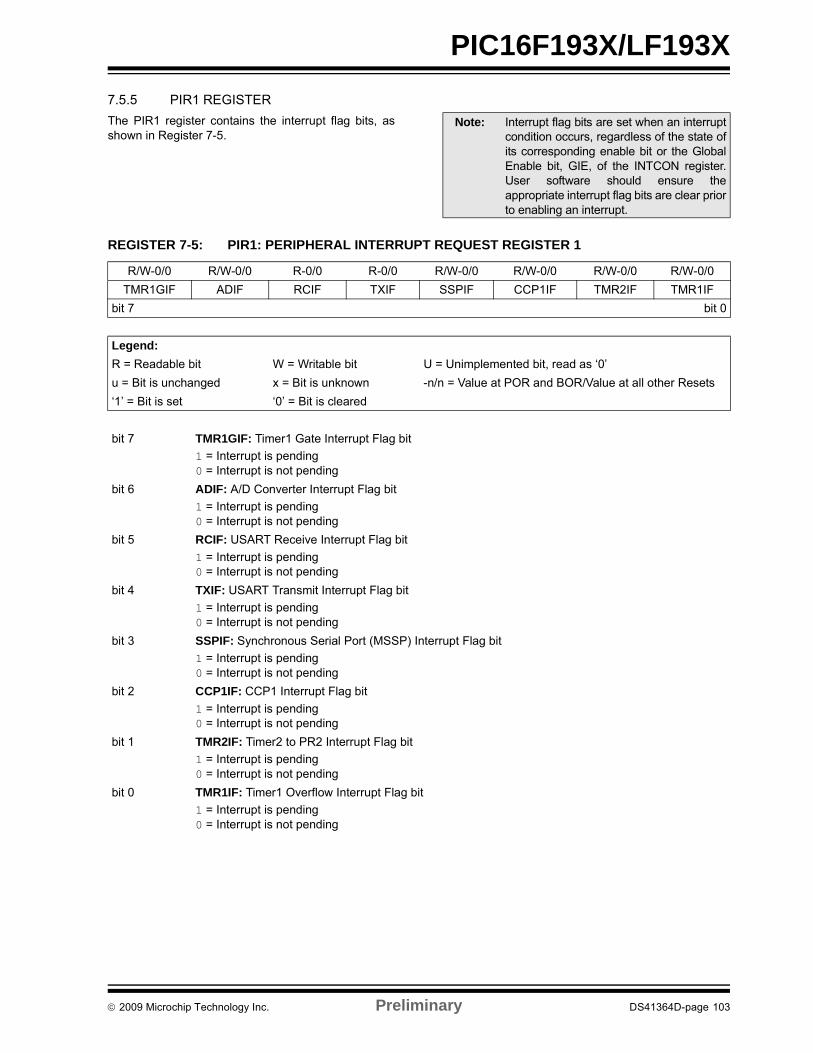
PIC16F193X/LF193X
7.5.5 PIR1 REGISTER
The PIR1 register contains the interrupt flag bits, asshown in Register 7-5.
Note: Interrupt flag bits are set when an interruptcondition occurs, regardless of the state ofits corresponding enable bit or the GlobalEnable bit, GIE, of the INTCON register.User software should ensure theappropriate interrupt flag bits are clear priorto enabling an interrupt.
REGISTER 7-5: PIR1: PERIPHERAL INTERRUPT REQUEST REGISTER 1
R/W-0/0 R/W-0/0 R-0/0 R-0/0 R/W-0/0 R/W-0/0 R/W-0/0 R/W-0/0
TMR1GIF ADIF RCIF TXIF SSPIF CCP1IF TMR2IF TMR1IF
bit 7 bit 0
Legend:
R = Readable bit W = Writable bit U = Unimplemented bit, read as ‘0’
u = Bit is unchanged x = Bit is unknown -n/n = Value at POR and BOR/Value at all other Resets
‘1’ = Bit is set ‘0’ = Bit is cleared
bit 7 TMR1GIF: Timer1 Gate Interrupt Flag bit
1 = Interrupt is pending0 = Interrupt is not pending
bit 6 ADIF: A/D Converter Interrupt Flag bit
1 = Interrupt is pending0 = Interrupt is not pending
bit 5 RCIF: USART Receive Interrupt Flag bit
1 = Interrupt is pending0 = Interrupt is not pending
bit 4 TXIF: USART Transmit Interrupt Flag bit
1 = Interrupt is pending0 = Interrupt is not pending
bit 3 SSPIF: Synchronous Serial Port (MSSP) Interrupt Flag bit
1 = Interrupt is pending0 = Interrupt is not pending
bit 2 CCP1IF: CCP1 Interrupt Flag bit
1 = Interrupt is pending0 = Interrupt is not pending
bit 1 TMR2IF: Timer2 to PR2 Interrupt Flag bit
1 = Interrupt is pending0 = Interrupt is not pending
bit 0 TMR1IF: Timer1 Overflow Interrupt Flag bit
1 = Interrupt is pending0 = Interrupt is not pending
2009 Microchip Technology Inc. Preliminary DS41364D-page 103

PIC16F193X/LF193X
7.5.6 PIR2 REGISTER
The PIR2 register contains the interrupt flag bits, asshown in Register 7-6.
Note: Interrupt flag bits are set when an interruptcondition occurs, regardless of the state ofits corresponding enable bit or the GlobalEnable bit, GIE, of the INTCON register.User software should ensure theappropriate interrupt flag bits are clear priorto enabling an interrupt.
REGISTER 7-6: PIR2: PERIPHERAL INTERRUPT REQUEST REGISTER 2
R/W-0/0 R/W-0/0 R/W-0/0 R/W-0/0 R/W-0/0 R/W-0/0 U-0 R/W-0/0
OSFIF C2IF C1IF EEIF BCLIF LCDIF — CCP2IF
bit 7 bit 0
Legend:
R = Readable bit W = Writable bit U = Unimplemented bit, read as ‘0’
u = Bit is unchanged x = Bit is unknown -n/n = Value at POR and BOR/Value at all other Resets
‘1’ = Bit is set ‘0’ = Bit is cleared
bit 7 OSFIF: Oscillator Fail Interrupt Flag
1 = Interrupt is pending0 = Interrupt is not pending
bit 6 C2IF: Comparator C2 Interrupt Flag
1 = Interrupt is pending0 = Interrupt is not pending
bit 5 C1IF: Comparator C1 Interrupt Flag
1 = Interrupt is pending0 = Interrupt is not pending
bit 4 EEIF: EEPROM Write Completion Interrupt Flag bit
1 = Interrupt is pending0 = Interrupt is not pending
bit 3 BCLIF: MSSP Bus Collision Interrupt Flag bit
1 = Interrupt is pending0 = Interrupt is not pending
bit 2 LCDIF: LCD Module Interrupt Flag bit
1 = Interrupt is pending0 = Interrupt is not pending
bit 1 Unimplemented: Read as ‘0’
bit 0 CCP2IF: CCP2 Interrupt Flag bit
1 = Interrupt is pending0 = Interrupt is not pending
DS41364D-page 104 Preliminary 2009 Microchip Technology Inc.

PIC16F193X/LF193X
7.5.7 PIR3 REGISTER
The PIR3 register contains the interrupt flag bits, asshown in Register 7-7.
Note: Interrupt flag bits are set when an interruptcondition occurs, regardless of the state ofits corresponding enable bit or the GlobalEnable bit, GIE, of the INTCON register.User software should ensure theappropriate interrupt flag bits are clear priorto enabling an interrupt.
REGISTER 7-7: PIR3: PERIPHERAL INTERRUPT REQUEST REGISTER 3
R/W-0/0 R/W-0/0 R/W-0/0 R/W-0/0 R/W-0/0 R/W-0/0 R/W-0/0 R/W-0/0
— CCP5IF CCP4IF CCP3IF TMR6IF — TMR4IF —
bit 7 bit 0
Legend:
R = Readable bit W = Writable bit U = Unimplemented bit, read as ‘0’
u = Bit is unchanged x = Bit is unknown -n/n = Value at POR and BOR/Value at all other Resets
‘1’ = Bit is set ‘0’ = Bit is cleared
bit 7 Unimplemented: Read as ‘0’
bit 6 CCP5IF: CCP5 Interrupt Flag bit
1 = Interrupt is pending0 = Interrupt is not pending
bit 5 CCP4IF: CCP4 Interrupt Flag bit
1 = Interrupt is pending0 = Interrupt is not pending
bit 4 CCP3IF: CCP3 Interrupt Flag bit
1 = Interrupt is pending0 = Interrupt is not pending
bit 3 TMR6IF: TMR6 to PR6 Match Interrupt Flag bit
1 = Interrupt is pending0 = Interrupt is not pending
bit 2 Unimplemented: Read as ‘0’
bit 1 TMR4IF: TMR4 to PR4 Match Interrupt Flag bit
1 = Interrupt is pending0 = Interrupt is not pending
bit 0 Unimplemented: Read as ‘0’
2009 Microchip Technology Inc. Preliminary DS41364D-page 105

PIC16F193X/LF193X
TABLE 7-1: SUMMARY OF REGISTERS ASSOCIATED WITH INTERRUPTS
Name Bit 7 Bit 6 Bit 5 Bit 4 Bit 3 Bit 2 Bit 1 Bit 0Register on Page
INTCON GIE PEIE TMR0IE INTE IOCIE TMR0IF INTF IOCIF 99
OPTION_REG WPUEN INTEDG TMROCS TMROSE PSA PS<2:0> 191
PIE1 TMR1GIE ADIE RCIE TXIE SSPIE CCP1IE TMR2IE TMR1IE 100
PIE2 OSFIE C2IE C1IE EEIE BCLIE LCDIE — CCP2IE 101
PIE3 — CCP5IE CCP4IE CCP3IE TMR6IE — TMR4IE — 102
PIR1 TMR1GIF ADIF RCIF TXIF SSPIF CCP1IF TMR2IF TMR1IF 103
PIR2 OSFIF C2IF C1IF EEIF BCLIF LCDIF — CCP2IF 104
PIR3 — CCP5IF CCP4IF CCP3IF TMR6IF — TMR4IF — 105
Legend: — = unimplemented location, read as ‘0’. Shaded cells are not used by Interrupts.
DS41364D-page 106 Preliminary 2009 Microchip Technology Inc.

PIC16F193X/LF193X
8.0 LOW DROPOUT (LDO) VOLTAGE REGULATOR
The PIC16F193X has an internal Low DropoutRegulator (LDO) which provides operation above 3.6V.The LDO regulates a voltage for the internal devicelogic while permitting the VDD and I/O pins to operateat a higher voltage. There is no user enable/disablecontrol available for the LDO, it is always active. ThePIC16LF193X operates at a maximum VDD of 3.6V anddoes not incorporate an LDO.
A device I/O pin may be configured as the LDO voltageoutput, identified as the VCAP pin. Although notrequired, an external low-ESR capacitor may be con-nected to the VCAP pin for additional regulator stability.
The VCAPEN<1:0> bits of Configuration Word 2 deter-mines which pin is assigned as the VCAP pin. Refer toTable 8-1.
On power-up, the external capacitor will load the LDOvoltage regulator. To prevent erroneous operation, thedevice is held in Reset while a constant current sourcecharges the external capacitor. After the cap is fullycharged, the device is released from Reset. For moreinformation on recommended capacitor values and theconstant current rate, refer to the LDO RegulatorCharacteristics Table in Section 29.0 “ElectricalSpecifications”.
TABLE 8-2: SUMMARY OF CONFIGURATION WORD WITH LDO
TABLE 8-1: VCAPEN<1:0> SELECT BITS
VCAPEN<1:0> Pin
00 RA0
01 RA5
10 RA6
11 No Vcap
Name Bits Bit -/7 Bit -/6 Bit 13/5 Bit 12/4 Bit 11/3 Bit 10/2 Bit 9/1 Bit 8/0Register on Page
CONFIG213:8 — — LVP DEBUG — BORV STVREN PLLEN
667:0 — — VCAPEN1(1) VCAPEN0(1) — — WRT1 WRT0
Legend: — = unimplemented locations read as ‘0’. Shaded cells are not used by LDO.Note 1: PIC16F193X only.
2009 Microchip Technology Inc. Preliminary DS41364D-page 107

PIC16F193X/LF193X
NOTES:
DS41364D-page 108 Preliminary 2009 Microchip Technology Inc.

PIC16F193X/LF193X
9.0 POWER-DOWN MODE (SLEEP)
The Power-down mode is entered by executing aSLEEP instruction.
Upon entering Sleep mode, the following conditionsexist:
1. WDT will be cleared but keeps running, ifenabled for operation during Sleep.
2. PD bit of the STATUS register is cleared.
3. TO bit of the STATUS register is set.
4. CPU clock is disabled.
5. 31 kHz LFINTOSC is unaffected and peripheralsthat operate from it may continue operation inSleep.
6. Timer1 oscillator is unaffected and peripheralsthat operate from it may continue operation inSleep.
7. ADC is unaffected, if the dedicated FRC clock isselected.
8. Capacitive Sensing oscillator is unaffected.
9. I/O ports maintain the status they had beforeSLEEP was executed (driving high, low or high-impedance).
10. Resets other than WDT are not affected bySleep mode.
Refer to individual chapters for more details onperipheral operation during Sleep.
To minimize current consumption, the following condi-tions should be considered:
• I/O pins should not be floating
• External circuitry sinking current from I/O pins
• Internal circuitry sourcing current from I/O pins
• Current draw from pins with internal weak pull-ups
• Modules using 31 kHz LFINTOSC
• Modules using Timer1 oscillator
I/O pins that are high-impedance inputs should bepulled to VDD or VSS externally to avoid switching cur-rents caused by floating inputs.
Examples of internal circuitry that might be sourcingcurrent include modules such as the DAC and FVRmodules. See Section 16.0 “Digital-to-Analog Con-verter (DAC) Module” and Section 14.0 “Fixed Volt-age Reference (FVR)” for more information on thesemodules.
9.1 Wake-up from Sleep
The device can wake-up from Sleep through one of thefollowing events:
1. External Reset input on MCLR pin, if enabled
2. BOR Reset, if enabled
3. POR Reset
4. Watchdog Timer, if enabled
5. Any external interrupt
6. Interrupts by peripherals capable of running dur-ing Sleep (see individual peripheral for moreinformation)
The first three events will cause a device Reset. Thelast three events are considered a continuation of pro-gram execution. To determine whether a device Resetor wake-up event occurred, refer to Section 6.10“Determining the Cause of a Reset”.
When the SLEEP instruction is being executed, the nextinstruction (PC + 1) is prefetched. For the device towake-up through an interrupt event, the correspondinginterrupt enable bit must be enabled. Wake-up willoccur regardless of the state of the GIE bit. If the GIEbit is disabled, the device continues execution at theinstruction after the SLEEP instruction. If the GIE bit isenabled, the device executes the instruction after theSLEEP instruction, the device will call the Interrupt Ser-vice Routine. In cases where the execution of theinstruction following SLEEP is not desirable, the usershould have a NOP after the SLEEP instruction.
The WDT is cleared when the device wakes up fromSleep, regardless of the source of wake-up.
2009 Microchip Technology Inc. Preliminary DS41364D-page 109

PIC16F193X/LF193X
9.1.1 WAKE-UP USING INTERRUPTS
When global interrupts are disabled (GIE cleared) andany interrupt source has both its interrupt enable bitand interrupt flag bit set, one of the following will occur:
• If the interrupt occurs before the execution of a SLEEP instruction
- SLEEP instruction will execute as a NOP.
- WDT and WDT prescaler will not be cleared
- TO bit of the STATUS register will not be set
- PD bit of the STATUS register will not be cleared.
• If the interrupt occurs during or after the execu-tion of a SLEEP instruction
- SLEEP instruction will be completely exe-cuted
- Device will immediately wake-up from Sleep
- WDT and WDT prescaler will be cleared
- TO bit of the STATUS register will be set
- PD bit of the STATUS register will be cleared.
Even if the flag bits were checked before executing aSLEEP instruction, it may be possible for flag bits tobecome set before the SLEEP instruction completes. Todetermine whether a SLEEP instruction executed, testthe PD bit. If the PD bit is set, the SLEEP instructionwas executed as a NOP.
FIGURE 9-1: WAKE-UP FROM SLEEP THROUGH INTERRUPT
TABLE 9-1: SUMMARY OF REGISTERS ASSOCIATED WITH POWER-DOWN MODE
Q1 Q2 Q3 Q4 Q1 Q2 Q3 Q4 Q1 Q1 Q2 Q3 Q4 Q1 Q2 Q3 Q4 Q1 Q2 Q3 Q4 Q1 Q2 Q3 Q4
OSC1(1)
CLKOUT(2)
Interrupt flag
GIE bit(INTCON reg.)
Instruction FlowPC
InstructionFetched
InstructionExecuted
PC PC + 1 PC + 2
Inst(PC) = Sleep
Inst(PC - 1)
Inst(PC + 1)
Sleep
Processor inSleep
Interrupt Latency(4)
Inst(PC + 2)
Inst(PC + 1)
Inst(0004h) Inst(0005h)
Inst(0004h)Dummy Cycle
PC + 2 0004h 0005h
Dummy Cycle
TOST(3)
PC + 2
Note 1: XT, HS or LP Oscillator mode assumed.2: CLKOUT is not available in XT, HS, or LP Oscillator modes, but shown here for timing reference.3: TOST = 1024 TOSC (drawing not to scale). This delay applies only to XT, HS or LP Oscillator modes.4: GIE = 1 assumed. In this case after wake-up, the processor calls the ISR at 0004h. If GIE = 0, execution will continue in-line.
Name Bit 7 Bit 6 Bit 5 Bit 4 Bit 3 Bit 2 Bit 1 Bit 0Register on
Page
INTCON GIE PEIE TMR0IE INTE IOCIE TMR0IF INTF IOCIF 99
IOCBF IOCBF7 IOCBF6 IOCBF5 IOCBF4 IOCBF3 IOCBF2 IOCBF1 IOCBF0 150
IOCBN IOCBN7 IOCBN6 IOCBN5 IOCBN4 IOCBN3 IOCBN2 IOCBN1 IOCBN0 150
IOCBP IOCBP7 IOCBP6 IOCBP5 IOCBP4 IOCBP3 IOCBP2 IOCBP1 IOCBP0 150
PIE1 TMR1GIE ADIE RCIE TXIE SSPIE CCP1IE TMR2IE TMR1IE 100
PIE2 OSFIE C2IE C1IE EEIE BCLIE LCDIE — CCP2IE 101
PIE3 — CCP5IE CCP4IE CCP3IE TMR6IE — TMR4IE — 102
PIR1 TMR1GIF ADIF RCIF TXIF SSPIF CCP1IF TMR2IF TMR1IF 103
PIR2 OSFIF C2IF C1IF EEIF BCLIF LCDIF — CCP2IF 104
PIR3 — CCP5IF CCP4IF CCP3IF TMR6IF — TMR4IF — 105
STATUS — — — TO PD Z DC C 29
WDTCON — — WDTPS<4:0> SWDTEN 113
Legend: — = unimplemented location, read as ‘0’. Shaded cells are not used in Power-down mode.
DS41364D-page 110 Preliminary 2009 Microchip Technology Inc.

PIC16F193X/LF193X
10.0 WATCHDOG TIMER
The Watchdog Timer is a system timer that generatesa Reset if the firmware does not issue a CLRWDTinstruction within the time-out period. The WatchdogTimer is typically used to recover the system fromunexpected events.
The WDT has the following features:
• Independent clock source
• Multiple operating modes
- WDT is always on
- WDT is off when in Sleep
- WDT is controlled by software
- WDT is always off
• Configurable time-out period is from 1 ms to 256 seconds (typical)
• Multiple Reset conditions
• Operation during Sleep
FIGURE 10-1: WATCHDOG TIMER BLOCK DIAGRAM
LFINTOSC23-bit Programmable
Prescaler WDTWDT Time-out
WDTPS<4:0>
SWDTEN
Sleep
WDTE<1:0> = 11
WDTE<1:0> = 01
WDTE<1:0> = 10
2009 Microchip Technology Inc. Preliminary DS41364D-page 111

PIC16F193X/LF193X
10.1 Independent Clock Source
The WDT derives its time base from the 31 kHzLFINTOSC internal oscillator.
10.2 WDT Operating Modes
The Watchdog Timer module has four operating modescontrolled by the WDTE<1:0> bits in ConfigurationWord 1. See Table 10-1.
10.2.1 WDT IS ALWAYS ON
When the WDTE bits of Configuration Word 1 are set to‘11’, the WDT is always on.
WDT protection is active during Sleep.
10.2.2 WDT IS OFF IN SLEEP
When the WDTE bits of Configuration Word 1 are set to‘10’, the WDT is on, except in Sleep.
WDT protection is not active during Sleep.
10.2.3 WDT CONTROLLED BY SOFTWARE
When the WDTE bits of Configuration Word 1 are set to‘01’, the WDT is controlled by the SWDTEN bit of theWDTCON register.
WDT protection is unchanged by Sleep. SeeTable 10-1 for more details.
TABLE 10-1: WDT OPERATING MODES
10.3 Time-Out Period
The WDTPS bits of the WDTCON register set thetime-out period from 1 ms to 256 seconds. After aReset, the default time-out period is 2 seconds.
10.4 Clearing the WDT
The WDT is cleared when any of the following condi-tions occur:
• Any Reset
• CLRWDT instruction is executed
• Device enters Sleep
• Device wakes up from Sleep
• Oscillator fail event
• WDT is disabled
• Oscillator Start-up TImer (OST) is running
See Table 10-2 for more information.
10.5 Operation During Sleep
When the device enters Sleep, the WDT is cleared. Ifthe WDT is enabled during Sleep, the WDT resumescounting.
When the device exits Sleep, the WDT is clearedagain. The WDT remains clear until the OST, ifenabled, completes. See Section 5.0 “OscillatorModule (With Fail-Safe Clock Monitor)” for moreinformation on the OST.
When a WDT time-out occurs while the device is inSleep, no Reset is generated. Instead, the device wakesup and resumes operation. The TO and PD bits in theSTATUS register are changed to indicate the event. SeeSection 3.0 “Memory Organization” and STATUSregister (Register 3-1) for more information.
WDTEConfig bits
SWDTENDevice Mode
WDT Mode
WDT_ON (11) X X Active
WDT_NSLEEP (10) X Awake Active
WDT_NSLEEP (10) X Sleep Disabled
WDT_SWDTEN (01) 1 X Active
WDT_SWDTEN (01) 0 X Disabled
WDT_OFF (00) X X Disabled
TABLE 10-2: WDT CLEARING CONDITIONS
Conditions WDT
WDTE<1:0> = 00
Cleared
WDTE<1:0> = 01 and SWDTEN = 0
WDTE<1:0> = 10 and enter Sleep
CLRWDT Command
Oscillator Fail Detected
Exit Sleep + System Clock = T1OSC, EXTRC, INTOSC, EXTCLK
Exit Sleep + System Clock = XT, HS, LP Cleared until the end of OST
Change INTOSC divider (IRCF bits) Unaffected
DS41364D-page 112 Preliminary 2009 Microchip Technology Inc.
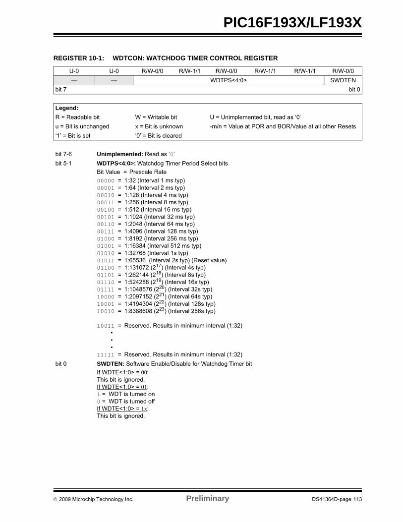
PIC16F193X/LF193X
REGISTER 10-1: WDTCON: WATCHDOG TIMER CONTROL REGISTER
U-0 U-0 R/W-0/0 R/W-1/1 R/W-0/0 R/W-1/1 R/W-1/1 R/W-0/0
— — WDTPS<4:0> SWDTEN
bit 7 bit 0
Legend:
R = Readable bit W = Writable bit U = Unimplemented bit, read as ‘0’
u = Bit is unchanged x = Bit is unknown -m/n = Value at POR and BOR/Value at all other Resets
‘1’ = Bit is set ‘0’ = Bit is cleared
bit 7-6 Unimplemented: Read as ‘0’
bit 5-1 WDTPS<4:0>: Watchdog Timer Period Select bits
Bit Value = Prescale Rate
00000 = 1:32 (Interval 1 ms typ)00001 = 1:64 (Interval 2 ms typ)00010 = 1:128 (Interval 4 ms typ)00011 = 1:256 (Interval 8 ms typ)00100 = 1:512 (Interval 16 ms typ)00101 = 1:1024 (Interval 32 ms typ)00110 = 1:2048 (Interval 64 ms typ)00111 = 1:4096 (Interval 128 ms typ)01000 = 1:8192 (Interval 256 ms typ)01001 = 1:16384 (Interval 512 ms typ)01010 = 1:32768 (Interval 1s typ)01011 = 1:65536 (Interval 2s typ) (Reset value)01100 = 1:131072 (217) (Interval 4s typ)01101 = 1:262144 (218) (Interval 8s typ)01110 = 1:524288 (219) (Interval 16s typ)01111 = 1:1048576 (220) (Interval 32s typ)10000 = 1:2097152 (221) (Interval 64s typ)10001 = 1:4194304 (222) (Interval 128s typ)10010 = 1:8388608 (223) (Interval 256s typ)
10011 = Reserved. Results in minimum interval (1:32) • • •
11111 = Reserved. Results in minimum interval (1:32)
bit 0 SWDTEN: Software Enable/Disable for Watchdog Timer bit
If WDTE<1:0> = 00:This bit is ignored.If WDTE<1:0> = 01:1 = WDT is turned on0 = WDT is turned offIf WDTE<1:0> = 1x:This bit is ignored.
2009 Microchip Technology Inc. Preliminary DS41364D-page 113

PIC16F193X/LF193X
NOTES:
DS41364D-page 114 Preliminary 2009 Microchip Technology Inc.

PIC16F193X/LF193X
11.0 DATA EEPROM AND FLASH PROGRAM MEMORY CONTROL
The Data EEPROM and Flash program memory arereadable and writable during normal operation (full VDD
range). These memories are not directly mapped in theregister file space. Instead, they are indirectlyaddressed through the Special Function Registers(SFRs). There are six SFRs used to access thesememories:
• EECON1
• EECON2
• EEDATL
• EEDATH
• EEADRL
• EEADRH
When interfacing the data memory block, EEDATLholds the 8-bit data for read/write, and EEADRL holdsthe address of the EEDATL location being accessed.These devices have 256 bytes of data EEPROM withan address range from 0h to 0FFh.
When accessing the program memory block, the EED-ATH:EEDATL register pair forms a 2-byte word thatholds the 14-bit data for read/write, and the EEADRLand EEADRH registers form a 2-byte word that holdsthe 15-bit address of the program memory locationbeing read.
The EEPROM data memory allows byte read and write.An EEPROM byte write automatically erases the loca-tion and writes the new data (erase before write).
The write time is controlled by an on-chip timer. Thewrite/erase voltages are generated by an on-chipcharge pump rated to operate over the voltage range ofthe device for byte or word operations.
Depending on the setting of the Flash ProgramMemory Self Write Enable bits WRT<1:0> of theConfiguration Word 2, the device may or may not beable to write certain blocks of the program memory.However, reads from the program memory are alwaysallowed.
When the device is code-protected, the deviceprogrammer can no longer access data or programmemory. When code-protected, the CPU may continueto read and write the data EEPROM memory and Flashprogram memory.
11.1 EEADRL and EEADRH Registers
The EEADRH:EEADRL register pair can address up toa maximum of 256 bytes of data EEPROM or up to amaximum of 32K words of program memory.
When selecting a program address value, the MSB ofthe address is written to the EEADRH register and theLSB is written to the EEADRL register. When selectinga EEPROM address value, only the LSB of the addressis written to the EEADRL register.
11.1.1 EECON1 AND EECON2 REGISTERS
EECON1 is the control register for EE memoryaccesses.
Control bit EEPGD determines if the access will be aprogram or data memory access. When clear, anysubsequent operations will operate on the EEPROMmemory. When set, any subsequent operations willoperate on the program memory. On Reset, EEPROM isselected by default.
Control bits RD and WR initiate read and write,respectively. These bits cannot be cleared, only set, insoftware. They are cleared in hardware at completionof the read or write operation. The inability to clear theWR bit in software prevents the accidental, prematuretermination of a write operation.
The WREN bit, when set, will allow a write operation tooccur. On power-up, the WREN bit is clear. TheWRERR bit is set when a write operation is interruptedby a Reset during normal operation. In these situations,following Reset, the user can check the WRERR bitand execute the appropriate error handling routine.
Interrupt flag bit EEIF of the PIR2 register is set whenwrite is complete. It must be cleared in the software.
Reading EECON2 will read all ‘0’s. The EECON2 reg-ister is used exclusively in the data EEPROM writesequence. To enable writes, a specific pattern must bewritten to EECON2.
2009 Microchip Technology Inc. Preliminary DS41364D-page 115
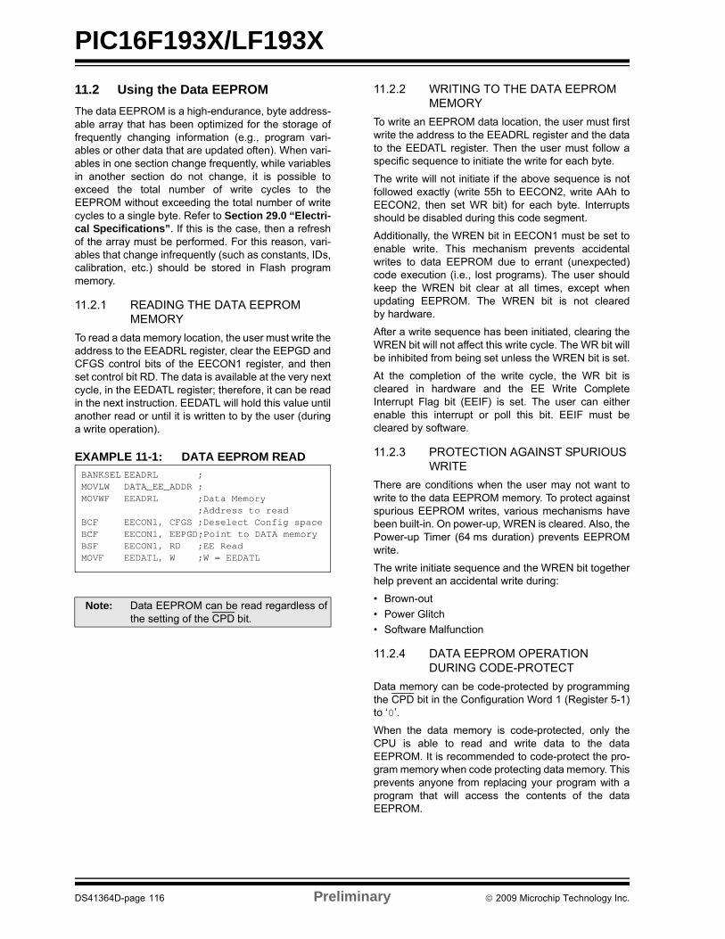
PIC16F193X/LF193X
11.2 Using the Data EEPROM
The data EEPROM is a high-endurance, byte address-able array that has been optimized for the storage offrequently changing information (e.g., program vari-ables or other data that are updated often). When vari-ables in one section change frequently, while variablesin another section do not change, it is possible toexceed the total number of write cycles to theEEPROM without exceeding the total number of writecycles to a single byte. Refer to Section 29.0 “Electri-cal Specifications”. If this is the case, then a refreshof the array must be performed. For this reason, vari-ables that change infrequently (such as constants, IDs,calibration, etc.) should be stored in Flash programmemory.
11.2.1 READING THE DATA EEPROM MEMORY
To read a data memory location, the user must write theaddress to the EEADRL register, clear the EEPGD andCFGS control bits of the EECON1 register, and thenset control bit RD. The data is available at the very nextcycle, in the EEDATL register; therefore, it can be readin the next instruction. EEDATL will hold this value untilanother read or until it is written to by the user (duringa write operation).
EXAMPLE 11-1: DATA EEPROM READ
11.2.2 WRITING TO THE DATA EEPROM MEMORY
To write an EEPROM data location, the user must firstwrite the address to the EEADRL register and the datato the EEDATL register. Then the user must follow aspecific sequence to initiate the write for each byte.
The write will not initiate if the above sequence is notfollowed exactly (write 55h to EECON2, write AAh toEECON2, then set WR bit) for each byte. Interruptsshould be disabled during this code segment.
Additionally, the WREN bit in EECON1 must be set toenable write. This mechanism prevents accidentalwrites to data EEPROM due to errant (unexpected)code execution (i.e., lost programs). The user shouldkeep the WREN bit clear at all times, except whenupdating EEPROM. The WREN bit is not clearedby hardware.
After a write sequence has been initiated, clearing theWREN bit will not affect this write cycle. The WR bit willbe inhibited from being set unless the WREN bit is set.
At the completion of the write cycle, the WR bit iscleared in hardware and the EE Write CompleteInterrupt Flag bit (EEIF) is set. The user can eitherenable this interrupt or poll this bit. EEIF must becleared by software.
11.2.3 PROTECTION AGAINST SPURIOUS WRITE
There are conditions when the user may not want towrite to the data EEPROM memory. To protect againstspurious EEPROM writes, various mechanisms havebeen built-in. On power-up, WREN is cleared. Also, thePower-up Timer (64 ms duration) prevents EEPROMwrite.
The write initiate sequence and the WREN bit togetherhelp prevent an accidental write during:
• Brown-out
• Power Glitch
• Software Malfunction
11.2.4 DATA EEPROM OPERATION DURING CODE-PROTECT
Data memory can be code-protected by programmingthe CPD bit in the Configuration Word 1 (Register 5-1)to ‘0’.
When the data memory is code-protected, only theCPU is able to read and write data to the dataEEPROM. It is recommended to code-protect the pro-gram memory when code protecting data memory. Thisprevents anyone from replacing your program with aprogram that will access the contents of the dataEEPROM.
Note: Data EEPROM can be read regardless ofthe setting of the CPD bit.
BANKSEL EEADRL ;MOVLW DATA_EE_ADDR ;MOVWF EEADRL ;Data Memory
;Address to readBCF EECON1, CFGS ;Deselect Config spaceBCF EECON1, EEPGD;Point to DATA memoryBSF EECON1, RD ;EE ReadMOVF EEDATL, W ;W = EEDATL
DS41364D-page 116 Preliminary 2009 Microchip Technology Inc.
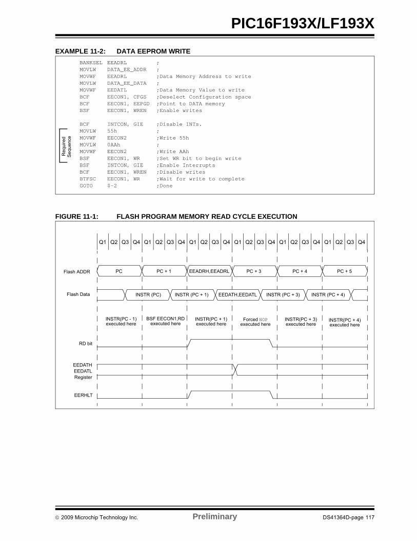
PIC16F193X/LF193X
EXAMPLE 11-2: DATA EEPROM WRITE
FIGURE 11-1: FLASH PROGRAM MEMORY READ CYCLE EXECUTION
BANKSEL EEADRL ;MOVLW DATA_EE_ADDR ;MOVWF EEADRL ;Data Memory Address to writeMOVLW DATA_EE_DATA ;MOVWF EEDATL ;Data Memory Value to writeBCF EECON1, CFGS ;Deselect Configuration spaceBCF EECON1, EEPGD ;Point to DATA memoryBSF EECON1, WREN ;Enable writes
BCF INTCON, GIE ;Disable INTs.MOVLW 55h ;MOVWF EECON2 ;Write 55hMOVLW 0AAh ;MOVWF EECON2 ;Write AAhBSF EECON1, WR ;Set WR bit to begin writeBSF INTCON, GIE ;Enable InterruptsBCF EECON1, WREN ;Disable writesBTFSC EECON1, WR ;Wait for write to completeGOTO $-2 ;Done
Re
quir
edS
equ
ence
Q1 Q2 Q3 Q4 Q1 Q2 Q3 Q4 Q1 Q2 Q3 Q4 Q1 Q2 Q3 Q4 Q1 Q2 Q3 Q4 Q1 Q2 Q3 Q4
BSF EECON1,RDexecuted here
INSTR(PC + 1)executed here
Forced NOPexecuted here
PC PC + 1 EEADRH,EEADRL PC+3 PC + 5Flash ADDR
RD bit
EEDATH,EEDATL
PC + 3 PC + 4
INSTR (PC + 1)
INSTR(PC - 1)executed here
INSTR(PC + 3)executed here
INSTR(PC + 4)executed here
Flash Data
EEDATHEEDATLRegister
EERHLT
INSTR (PC) INSTR (PC + 3) INSTR (PC + 4)
2009 Microchip Technology Inc. Preliminary DS41364D-page 117

PIC16F193X/LF193X
11.3 Flash Program Memory Overview
It is important to understand the Flash program mem-ory structure for erase and programming operations.Flash Program memory is arranged in rows. A row con-sists of a fixed number of 14-bit program memorywords. A row is the minimum block size that can beerased by user software.
Flash program memory may only be written or erasedif the destination address is in a segment of memorythat is not write-protected, as defined in bits WRT<1:0>of Configuration Word 2.
After a row has been erased, the user can reprogramall or a portion of this row. Data to be written into theprogram memory row is written to 14-bit wide data writelatches. These write latches are not directly accessibleto the user, but may be loaded via sequential writes tothe EEDATH:EEDATL register pair.
The number of data write latches is not equivalent tothe number of row locations. During programming, usersoftware will need to fill the set of write latches and ini-tiate a programming operation multiple times in order tofully reprogram an erased row. For example, a devicewith a row size of 32 words and eight write latches willneed to load the write latches with data and initiate aprogramming operation four times.
The size of a program memory row and the number ofprogram memory write latches may vary by device.See Table 11-1 for details.
11.3.1 READING THE FLASH PROGRAM MEMORY
To read a program memory location, the user must:
1. Write the Least and Most Significant addressbits to the EEADRH:EEADRL register pair.
2. Clear the CFGS bit of the EECON1 register.
3. Set the EEPGD control bit of the EECON1register.
4. Then, set control bit RD of the EECON1 register.
Once the read control bit is set, the program memoryFlash controller will use the second instruction cycle toread the data. This causes the second instructionimmediately following the “BSF EECON1,RD” instructionto be ignored. The data is available in the very next cycle,in the EEDATH:EEDATL register pair; therefore, it canbe read as two bytes in the following instructions.
EEDATH:EEDATL register pair will hold this value untilanother read or until it is written to by the user.Note: If the user wants to modify only a portion
of a previously programmed row, then thecontents of the entire row must be readand saved in RAM prior to the erase.
TABLE 11-1: FLASH MEMORY ORGANIZATION BY DEVICE
DeviceErase Block (Row) Size/Boundary
Number of Write Latches/
Boundary
PIC16F193X/LF193X
32 words, EEADRL<4:0> =
00000
8 words,EEADRL<2:0> =
000
Note 1: The two instructions following a programmemory read are required to be NOPs.This prevents the user from executing atwo-cycle instruction on the nextinstruction after the RD bit is set.
2: Flash program memory can be readregardless of the setting of the CP bit.
DS41364D-page 118 Preliminary 2009 Microchip Technology Inc.
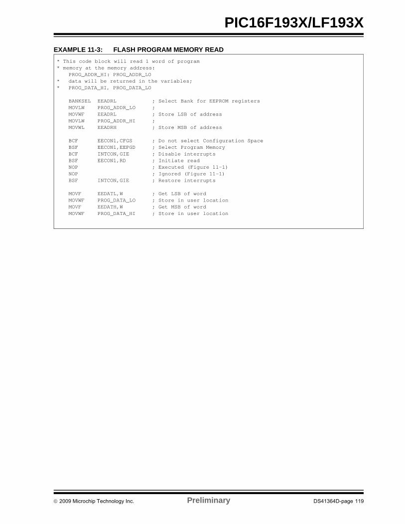
PIC16F193X/LF193X
EXAMPLE 11-3: FLASH PROGRAM MEMORY READ
* This code block will read 1 word of program* memory at the memory address:
PROG_ADDR_HI: PROG_ADDR_LO* data will be returned in the variables;* PROG_DATA_HI, PROG_DATA_LO
BANKSEL EEADRL ; Select Bank for EEPROM registersMOVLW PROG_ADDR_LO ; MOVWF EEADRL ; Store LSB of addressMOVLW PROG_ADDR_HI ; MOVWL EEADRH ; Store MSB of address
BCF EECON1,CFGS ; Do not select Configuration SpaceBSF EECON1,EEPGD ; Select Program MemoryBCF INTCON,GIE ; Disable interruptsBSF EECON1,RD ; Initiate readNOP ; Executed (Figure 11-1)NOP ; Ignored (Figure 11-1)BSF INTCON,GIE ; Restore interrupts
MOVF EEDATL,W ; Get LSB of wordMOVWF PROG_DATA_LO ; Store in user locationMOVF EEDATH,W ; Get MSB of wordMOVWF PROG_DATA_HI ; Store in user location
2009 Microchip Technology Inc. Preliminary DS41364D-page 119

PIC16F193X/LF193X
11.3.2 ERASING FLASH PROGRAM MEMORY
While executing code, program memory can only beerased by rows. To erase a row:
1. Load the EEADRH:EEADRL register pair withthe address of new row to be erased.
2. Clear the CFGS bit of the EECON1 register.
3. Set the EEPGD, FREE, and WREN bits of theEECON1 register.
4. Write 55h, then AAh, to EECON2 (Flashprogramming unlock sequence).
5. Set control bit WR of the EECON1 register tobegin the erase operation.
6. Poll the FREE bit in the EECON1 register todetermine when the row erase has completed.
See Example 11-4.
After the “BSF EECON1,WR” instruction, the processorrequires two cycles to set up the erase operation. Theuser must place two NOP instructions after the WR bit isset. The processor will halt internal operations for thetypical 2 ms erase time. This is not Sleep mode as theclocks and peripherals will continue to run. After theerase cycle, the processor will resume operation withthe third instruction after the EECON1 write instruction.
11.3.3 WRITING TO FLASH PROGRAM MEMORY
Program memory is programmed using the followingsteps:
1. Load the starting address of the word(s) to beprogrammed.
2. Load the write latches with data.
3. Initiate a programming operation.
4. Repeat steps 1 through 3 until all data is written.
Before writing to program memory, the word(s) to bewritten must be erased or previously unwritten. Pro-gram memory can only be erased one row at a time. Noautomatic erase occurs upon the initiation of the write.
Program memory can be written one or more words ata time. The maximum number of words written at onetime is equal to the number of write latches. SeeFigure 11-2 (block writes to program memory with 8write latches) for more details. The write latches arealigned to the address boundary defined by EEADRLas shown in Table 11-1. Write operations do not crossthese boundaries. At the completion of a programmemory write operation, the write latches are reset tocontain 0x3FFF.
The following steps should be completed to load thewrite latches and program a block of program memory.These steps are divided into two parts. First, all writelatches are loaded with data except for the last programmemory location. Then, the last write latch is loadedand the programming sequence is initiated. A specialunlock sequence is required to load a write latch withdata or initiate a Flash programming operation. Thisunlock sequence should not be interrupted.
1. Set the EEPGD and WREN bits of the EECON1register.
2. Clear the CFGS bit of the EECON1 register.
3. Set the LWLO bit of the EECON1 register. Whenthe LWLO bit of the EECON1 register is ‘1’, thewrite sequence will only load the write latchesand will not initiate the write to Flash programmemory.
4. Load the EEADRH:EEADRL register pair withthe address of the location to be written.
5. Load the EEDATH:EEDATL register pair withthe program memory data to be written.
6. Write 55h, then AAh, to EECON2, then set theWR bit of the EECON1 register (Flashprogramming unlock sequence). The write latchis now loaded.
7. Increment the EEADRH:EEADRL register pairto point to the next location.
8. Repeat steps 5 through 7 until all but the lastwrite latch has been loaded.
9. Clear the LWLO bit of the EECON1 register.When the LWLO bit of the EECON1 register is‘0’, the write sequence will initiate the write toFlash program memory.
10. Load the EEDATH:EEDATL register pair withthe program memory data to be written.
11. Write 55h, then AAh, to EECON2, then set theWR bit of the EECON1 register (Flashprogramming unlock sequence). The entirelatch block is now written to Flash programmemory.
It is not necessary to load the entire write latch blockwith user program data. However, the entire write latchblock will be written to program memory.
An example of the complete write sequence for eightwords is shown in Example 11-5. The initial address isloaded into the EEADRH:EEADRL register pair; theeight words of data are loaded using indirectaddressing.
Note: The code sequence provided inExample 11-5 must be repeated multipletimes to fully program an erased programmemory row.
DS41364D-page 120 Preliminary 2009 Microchip Technology Inc.
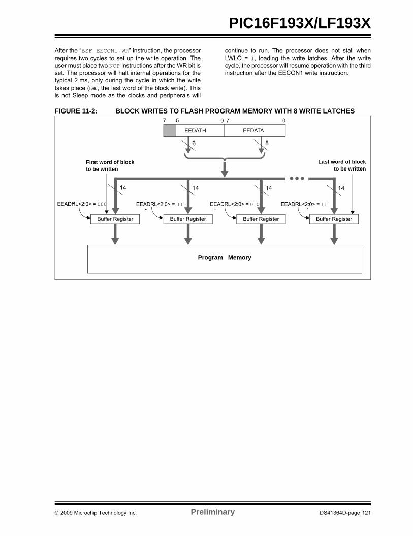
PIC16F193X/LF193X
After the “BSF EECON1,WR” instruction, the processorrequires two cycles to set up the write operation. Theuser must place two NOP instructions after the WR bit isset. The processor will halt internal operations for thetypical 2 ms, only during the cycle in which the writetakes place (i.e., the last word of the block write). Thisis not Sleep mode as the clocks and peripherals will
continue to run. The processor does not stall whenLWLO = 1, loading the write latches. After the writecycle, the processor will resume operation with the thirdinstruction after the EECON1 write instruction.
FIGURE 11-2: BLOCK WRITES TO FLASH PROGRAM MEMORY WITH 8 WRITE LATCHES
14 14 14 14
Program Memory
Buffer Register
EEADRL<2:0> = 000
Buffer Register
EEADRL<2:0> = 001
Buffer Register
EEADRL<2:0> = 010
Buffer Register
EEADRL<2:0> = 111
EEDATAEEDATH
7 5 0 7 0
6 8
First word of blockto be written
Last word of blockto be written
2009 Microchip Technology Inc. Preliminary DS41364D-page 121

PIC16F193X/LF193X
EXAMPLE 11-4: ERASING ONE ROW OF PROGRAM MEMORY -; This row erase routine assumes the following:; 1. A valid address within the erase block is loaded in ADDRH:ADDRL; 2. ADDRH and ADDRL are located in shared data memory 0x70 - 0x7F
BCF INTCON,GIE ; Disable ints so required sequences will execute properlyBANKSEL EEADRLMOVF ADDRL,W ; Load lower 8 bits of erase address boundaryMOVWF EEADRLMOVF ADDRH,W ; Load upper 6 bits of erase address boundaryMOVWF EEADRHBSF EECON1,EEPGD ; Point to program memoryBCF EECON1,CFGS ; Not configuration spaceBSF EECON1,FREE ; Specify an erase operationBSF EECON1,WREN ; Enable writes
MOVLW 55h ; Start of required sequence to initiate eraseMOVWF EECON2 ; Write 55hMOVLW 0AAh ;MOVWF EECON2 ; Write AAhBSF EECON1,WR ; Set WR bit to begin eraseNOP ; Any instructions here are ignored as processor
; halts to begin erase sequenceNOP ; Processor will stop here and wait for erase complete.
; after erase processor continues with 3rd instruction
BCF EECON1,WREN ; Disable writesBSF INTCON,GIE ; Enable interrupts
Re
qu
ire
dS
eq
ue
nce
DS41364D-page 122 Preliminary 2009 Microchip Technology Inc.

PIC16F193X/LF193X
EXAMPLE 11-5: WRITING TO FLASH PROGRAM MEMORY
; This write routine assumes the following:; 1. The 16 bytes of data are loaded, starting at the address in DATA_ADDR; 2. Each word of data to be written is made up of two adjacent bytes in DATA_ADDR,; stored in little endian format; 3. A valid starting address (the least significant bits = 000) is loaded in ADDRH:ADDRL; 4. ADDRH and ADDRL are located in shared data memory 0x70 - 0x7F;
BCF INTCON,GIE ; Disable ints so required sequences will execute properlyBANKSEL EEADRH ; Bank 3MOVF ADDRH,W ; Load initial addressMOVWF EEADRH ;MOVF ADDRL,W ;MOVWF EEADRL ;MOVLW LOW DATA_ADDR ; Load initial data addressMOVWF FSR0L ;MOVLW HIGH DATA_ADDR ; Load initial data addressMOVWF FSR0H ;BSF EECON1,EEPGD ; Point to program memoryBCF EECON1,CFGS ; Not configuration spaceBSF EECON1,WREN ; Enable writesBSF EECON1,LWLO ; Only Load Write Latches
LOOPMOVIW INDF0++ ; Load first data byte into lowerMOVWF EEDATL ;MOVIW INDF0++ ; Load second data byte into upperMOVWF EEDATH ;
MOVF EEADRL,W ; Check if lower bits of address are '000'XORLW 0x07 ; Check if we're on the last of 8 addressesANDLW 0x07 ;BTFSC STATUS,Z ; Exit if last of eight words,GOTO START_WRITE ;
MOVLW 55h ; Start of required write sequence:MOVWF EECON2 ; Write 55hMOVLW 0AAh ;MOVWF EECON2 ; Write AAhBSF EECON1,WR ; Set WR bit to begin writeNOP ; Any instructions here are ignored as processor
; halts to begin write sequenceNOP ; Processor will stop here and wait for write to complete.
; After write processor continues with 3rd instruction.
INCF EEADRL,F ; Still loading latches Increment addressGOTO LOOP ; Write next latches
START_WRITEBCF EECON1,LWLO ; No more loading latches - Actually start Flash program
; memory write
MOVLW 55h ; Start of required write sequence:MOVWF EECON2 ; Write 55hMOVLW 0AAh ;MOVWF EECON2 ; Write AAhBSF EECON1,WR ; Set WR bit to begin writeNOP ; Any instructions here are ignored as processor
; halts to begin write sequenceNOP ; Processor will stop here and wait for write complete.
; after write processor continues with 3rd instructionBCF EECON1,WREN ; Disable writesBSF INTCON,GIE ; Enable interrupts
Re
qu
ire
dS
eq
ue
nce
Re
qu
ire
dS
eq
ue
nce
2009 Microchip Technology Inc. Preliminary DS41364D-page 123

PIC16F193X/LF193X
11.4 Modifying Flash Program Memory
When modifying existing data in a program memoryrow, and data within that row must be preserved, it mustfirst be read and saved in a RAM image. Programmemory is modified using the following steps:
1. Load the starting address of the row to be mod-ified.
2. Read the existing data from the row into a RAMimage.
3. Modify the RAM image to contain the new datato be written into program memory.
4. Load the starting address of the row to be rewrit-ten.
5. Erase the program memory row.
6. Load the write latches with data from the RAMimage.
7. Initiate a programming operation.
8. Repeat steps 6 and 7 as many times as requiredto reprogram the erased row.
11.5 User ID, Device ID and Configuration Word Access
Instead of accessing program memory or EEPROMdata memory, the User ID’s, Device ID/Revision ID andConfiguration Words can be accessed when CFGS = 1in the EECON1 register. This is the region that wouldbe pointed to by PC<15> = 1, but not all addresses areaccessible. Different access may exist for reads andwrites. Refer to Table 11-2.
When read access is initiated on an address outsidethe parameters listed in Table 11-2, the EEDATH:EED-ATL register pair is cleared.
TABLE 11-2: USER ID, DEVICE ID AND CONFIGURATION WORD ACCESS (CFGS = 1)
EXAMPLE 11-3: CONFIGURATION WORD AND DEVICE ID ACCESS
Address Function Read Access Write Access
8000h-8003h User IDs Yes Yes
8006h Device ID/Revision ID Yes No
8007h-8008h Configuration Words 1 and 2 Yes No
* This code block will read 1 word of program memory at the memory address:* PROG_ADDR_LO (must be 00h-08h) data will be returned in the variables;* PROG_DATA_HI, PROG_DATA_LO
BANKSEL EEADRL ; Select correct BankMOVLW PROG_ADDR_LO ; MOVWF EEADRL ; Store LSB of addressCLRF EEADRH ; Clear MSB of address
BSF EECON1,CFGS ; Select Configuration Space BCF INTCON,GIE ; Disable interruptsBSF EECON1,RD ; Initiate readNOP ; Executed (See Figure 11-1)NOP ; Ignored (See Figure 11-1)BSF INTCON,GIE ; Restore interrupts
MOVF EEDATL,W ; Get LSB of wordMOVWF PROG_DATA_LO ; Store in user locationMOVF EEDATH,W ; Get MSB of wordMOVWF PROG_DATA_HI ; Store in user location
DS41364D-page 124 Preliminary 2009 Microchip Technology Inc.
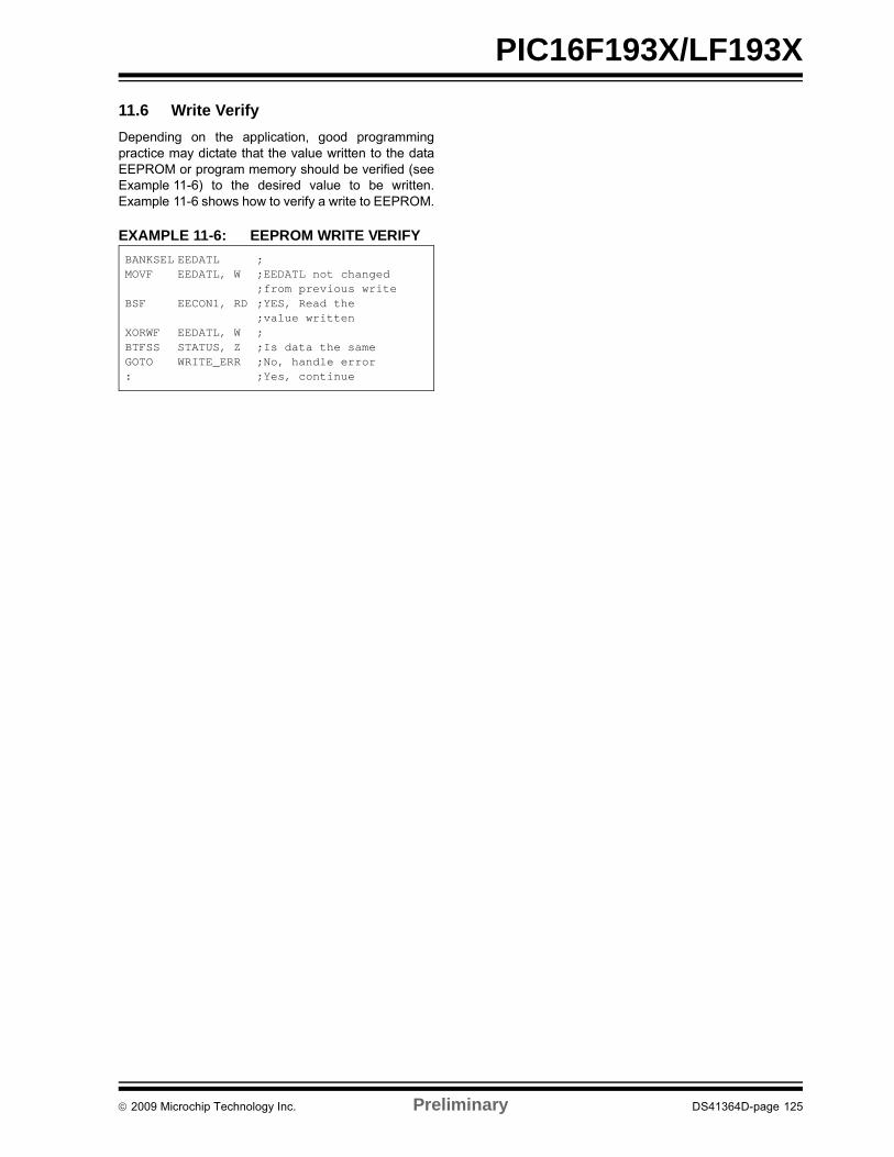
PIC16F193X/LF193X
11.6 Write Verify
Depending on the application, good programmingpractice may dictate that the value written to the dataEEPROM or program memory should be verified (seeExample 11-6) to the desired value to be written.Example 11-6 shows how to verify a write to EEPROM.
EXAMPLE 11-6: EEPROM WRITE VERIFY
BANKSEL EEDATL ;MOVF EEDATL, W ;EEDATL not changed
;from previous writeBSF EECON1, RD ;YES, Read the
;value writtenXORWF EEDATL, W ;BTFSS STATUS, Z ;Is data the sameGOTO WRITE_ERR ;No, handle error: ;Yes, continue
2009 Microchip Technology Inc. Preliminary DS41364D-page 125

PIC16F193X/LF193X
REGISTER 11-1: EEDATL: EEPROM DATA REGISTER
R/W-x/u R/W-x/u R/W-x/u R/W-x/u R/W-x/u R/W-x/u R/W-x/u R/W-x/u
EEDAT<7:0>
bit 7 bit 0
Legend:
R = Readable bit W = Writable bit U = Unimplemented bit, read as ‘0’
u = Bit is unchanged x = Bit is unknown -n/n = Value at POR and BOR/Value at all other Resets
‘1’ = Bit is set ‘0’ = Bit is cleared
bit 7-0 EEDAT<7:0>: Read/write value for EEPROM data byte or Least Significant bits of program memory
REGISTER 11-2: EEDATH: EEPROM DATA HIGH BYTE REGISTER
U-0 U-0 R/W-x/u R/W-x/u R/W-x/u R/W-x/u R/W-x/u R/W-x/u
— — EEDAT<13:8>
bit 7 bit 0
Legend:
R = Readable bit W = Writable bit U = Unimplemented bit, read as ‘0’
u = Bit is unchanged x = Bit is unknown -n/n = Value at POR and BOR/Value at all other Resets
‘1’ = Bit is set ‘0’ = Bit is cleared
bit 7-6 Unimplemented: Read as ‘0’
bit 5-0 EEDAT<13:8>: Read/write value for Most Significant bits of program memory
REGISTER 11-3: EEADRL: EEPROM ADDRESS REGISTER
R/W-0/0 R/W-0/0 R/W-0/0 R/W-0/0 R/W-0/0 R/W-0/0 R/W-0/0 R/W-0/0
EEADR<7:0>
bit 7 bit 0
Legend:
R = Readable bit W = Writable bit U = Unimplemented bit, read as ‘0’
u = Bit is unchanged x = Bit is unknown -n/n = Value at POR and BOR/Value at all other Resets
‘1’ = Bit is set ‘0’ = Bit is cleared
bit 7-0 EEADR<7:0>: Specifies the Least Significant bits for program memory address or EEPROM address
REGISTER 11-4: EEADRH: EEPROM ADDRESS HIGH BYTE REGISTER
U-0 R/W-0/0 R/W-0/0 R/W-0/0 R/W-0/0 R/W-0/0 R/W-0/0 R/W-0/0
— EEADR<14:8>
bit 7 bit 0
Legend:
R = Readable bit W = Writable bit U = Unimplemented bit, read as ‘0’
u = Bit is unchanged x = Bit is unknown -n/n = Value at POR and BOR/Value at all other Resets
‘1’ = Bit is set ‘0’ = Bit is cleared
bit 7 Unimplemented: Read as ‘0’
bit 6-0 EEADR<14:8>: Specifies the Most Significant bits for program memory address or EEPROM address
DS41364D-page 126 Preliminary 2009 Microchip Technology Inc.
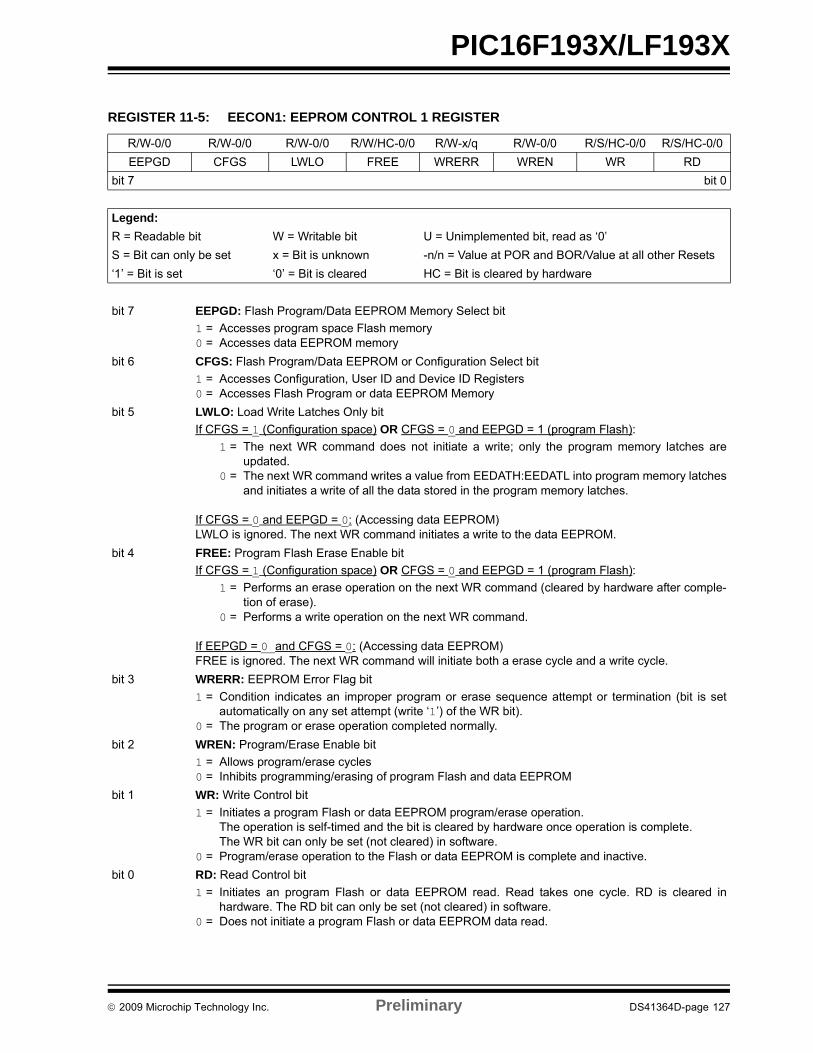
PIC16F193X/LF193X
REGISTER 11-5: EECON1: EEPROM CONTROL 1 REGISTER
R/W-0/0 R/W-0/0 R/W-0/0 R/W/HC-0/0 R/W-x/q R/W-0/0 R/S/HC-0/0 R/S/HC-0/0
EEPGD CFGS LWLO FREE WRERR WREN WR RD
bit 7 bit 0
Legend:
R = Readable bit W = Writable bit U = Unimplemented bit, read as ‘0’
S = Bit can only be set x = Bit is unknown -n/n = Value at POR and BOR/Value at all other Resets
‘1’ = Bit is set ‘0’ = Bit is cleared HC = Bit is cleared by hardware
bit 7 EEPGD: Flash Program/Data EEPROM Memory Select bit
1 = Accesses program space Flash memory0 = Accesses data EEPROM memory
bit 6 CFGS: Flash Program/Data EEPROM or Configuration Select bit
1 = Accesses Configuration, User ID and Device ID Registers0 = Accesses Flash Program or data EEPROM Memory
bit 5 LWLO: Load Write Latches Only bit
If CFGS = 1 (Configuration space) OR CFGS = 0 and EEPGD = 1 (program Flash):
1 = The next WR command does not initiate a write; only the program memory latches areupdated.
0 = The next WR command writes a value from EEDATH:EEDATL into program memory latchesand initiates a write of all the data stored in the program memory latches.
If CFGS = 0 and EEPGD = 0: (Accessing data EEPROM)LWLO is ignored. The next WR command initiates a write to the data EEPROM.
bit 4 FREE: Program Flash Erase Enable bit
If CFGS = 1 (Configuration space) OR CFGS = 0 and EEPGD = 1 (program Flash):
1 = Performs an erase operation on the next WR command (cleared by hardware after comple-tion of erase).
0 = Performs a write operation on the next WR command.
If EEPGD = 0 and CFGS = 0: (Accessing data EEPROM)FREE is ignored. The next WR command will initiate both a erase cycle and a write cycle.
bit 3 WRERR: EEPROM Error Flag bit
1 = Condition indicates an improper program or erase sequence attempt or termination (bit is setautomatically on any set attempt (write ‘1’) of the WR bit).
0 = The program or erase operation completed normally.
bit 2 WREN: Program/Erase Enable bit
1 = Allows program/erase cycles0 = Inhibits programming/erasing of program Flash and data EEPROM
bit 1 WR: Write Control bit
1 = Initiates a program Flash or data EEPROM program/erase operation. The operation is self-timed and the bit is cleared by hardware once operation is complete. The WR bit can only be set (not cleared) in software.
0 = Program/erase operation to the Flash or data EEPROM is complete and inactive.
bit 0 RD: Read Control bit
1 = Initiates an program Flash or data EEPROM read. Read takes one cycle. RD is cleared inhardware. The RD bit can only be set (not cleared) in software.
0 = Does not initiate a program Flash or data EEPROM data read.
2009 Microchip Technology Inc. Preliminary DS41364D-page 127

PIC16F193X/LF193X
TABLE 11-3: SUMMARY OF REGISTERS ASSOCIATED WITH DATA EEPROM
REGISTER 11-6: EECON2: EEPROM CONTROL 2 REGISTER
W-0/0 W-0/0 W-0/0 W-0/0 W-0/0 W-0/0 W-0/0 W-0/0
EEPROM Control Register 2
bit 7 bit 0
Legend:
R = Readable bit W = Writable bit U = Unimplemented bit, read as ‘0’
S = Bit can only be set x = Bit is unknown -n/n = Value at POR and BOR/Value at all other Resets
‘1’ = Bit is set ‘0’ = Bit is cleared
bit 7-0 Data EEPROM Unlock Pattern bits
To unlock writes, a 55h must be written first, followed by an AAh, before setting the WR bit of theEECON1 register. The value written to this register is used to unlock the writes. There are specifictiming requirements on these writes. Refer to Section 11.2.2 “Writing to the Data EEPROMMemory” for more information.
Name Bit 7 Bit 6 Bit 5 Bit 4 Bit 3 Bit 2 Bit 1 Bit 0Register on
Page
EECON1 EEPGD CFGS LWLO FREE WRERR WREN WR RD 127
EECON2 EEPROM Control Register 2 (not a physical register) 115*
EEADRL EEADRL<7:0> 126
EEADRH — EEADRH<6:0 126
EEDATL EEDATL<7:0> 126
EEDATH — — EEDATH<5:0> 126
INTCON GIE PEIE TMR0IE INTE IOCIE TMR0IF INTF IOCIF 99
PIE2 OSFIE C2IE C1IE EEIE BCLIE LCDIE — CCP2IE 101
PIR2 OSFIF C2IF C1IF EEIF BCLIF LCDIF — CCP2IF 104
Legend: — = unimplemented location, read as ‘0’. Shaded cells are not used by Data EEPROM module.* Page provides register information.
DS41364D-page 128 Preliminary 2009 Microchip Technology Inc.

PIC16F193X/LF193X
12.0 I/O PORTS
Depending on the device selected and peripheralsenabled, there are up to five ports available. In general,when a peripheral is enabled, that pin may not be usedas a general purpose I/O pin.
Each port has three registers for its operation. Theseregisters are:
• TRISx registers (data direction register)
• PORTx registers (reads the levels on the pins of the device)
• LATx registers (output latch)
The Data Latch (LATx registers) is useful forread-modify-write operations on the value that the I/Opins are driving.
A write operation to the LATx register has the sameaffect as a write to the corresponding PORTx register.A read of the LATx register reads of the values held inthe I/O PORT latches, while a read of the PORTxregister reads the actual I/O pin value.
Ports with analog functions also have an ANSELxregister which can disable the digital input and savepower. A simplified model of a generic I/O port, withoutthe interfaces to other peripherals, is shown inFigure 12-1.
FIGURE 12-1: GENERIC I/O PORT OPERATION
12.1 Alternate Pin Function
The Alternate Pin Function Control (APFCON) registeris used to steer specific peripheral input and outputfunctions between different pins. The APFCON registeris shown in Register 12-1. For this device family, thefollowing functions can be moved between differentpins.
• SS (Slave Select)
• P2B output
• CCP2/P2A output
• CCP3/P3A output
• Timer1 Gate
• SR Latch SRNQ output
• Comparator C2 output
These bits have no effect on the values of any TRISregister. PORT and TRIS overrides will be routed to thecorrect pin. The unselected pin will be unaffected.
QD
CK
Write LATx
Data Register
I/O pinRead PORTx
Write PORTx
TRISxRead LATx
Data Bus
To peripherals
ANSELx
VDD
VSS
2009 Microchip Technology Inc. Preliminary DS41364D-page 129

PIC16F193X/LF193X
REGISTER 12-1: APFCON: ALTERNATE PIN FUNCTION CONTROL REGISTER
U-0 R/W-0/0 R/W-0/0 R/W-0/0 R/W-0/0 R/W-0/0 R/W-0/0 R/W-0/0
— CCP3SEL T1GSEL P2BSEL SRNQSEL C2OUTSEL SSSEL CCP2SEL
bit 7 bit 0
Legend:
R = Readable bit W = Writable bit U = Unimplemented bit, read as ‘0’
u = bit is unchanged x = Bit is unknown -n/n = Value at POR and BOR/Value at all other Resets
‘1’ = Bit is set ‘0’ = Bit is cleared
bit 7 Unimplemented: Read as ‘0’.
bit 6 CCP3SEL: CCP3 Input/Output Pin Selection bit
For 28-Pin Devices (PIC16F1933/1936/1938):
0 = CCP3/P3A function is on RC6/TX/CK/CCP3/P3A/SEG91 = CCP3/P3A function is on RB5/AN13/CPS5/CCP3/P3A/T1G/COM1
For 40-Pin Devices (PIC16F1934/1937/1939):
0 = CCP3/P3A function is on RE0/AN5/CCP3/P3A/SEG211 = CCP3/P3A function is on RB5/AN13/CPS5/CCP3/P3A/T1G/COM1
bit 5 T1GSEL: Timer1 Gate Input Pin Selection bit
0 = T1G function is on RB5/AN13/CPS5/CCP3/P3A/T1G/COM11 = T1G function is on RC4/SDI/SDA/T1G/SEG11
bit 4 P2BSEL: CCP2 PWM B Output Pin Selection bit
For 28-Pin Devices (PIC16F1933/1936/1938):
0 = P2B function is on RC0/T1OSO/T1CKI/P2B1 = P2B function is on RB5/AN13/P2B/CPS5/T1G/COM1
For 40-Pin Devices (PIC16F1934/1937/1939):
0 = P2B function is on RC0/T1OSO/T1CKI/P2B1 = P2B function is on RD2/CPS10/P2B
bit 3 SRNQSEL: SR Latch nQ Output Pin Selection bit
0 = SRnQ function is on RA5/AN4/C2OUT/SRnQ/SS/CPS7/SEG5/VCAP
1 = SRnQ function is on RA0/AN0/C12IN0-/C2OUT/SRnQ/SS/SEG12/VCAP
bit 2 C2OUTSEL: Comparator C2 Output Pin Selection bit
0 = C2OUT function is on RA5/AN4/C2OUT/SRnQ/SS/CPS7/SEG5/VCAP
1 = C2OUT function is on RA0/AN0/C12IN0-/C2OUT/SRnQ/SS/SEG12/VCAP
bit 1 SSSEL: SS Input Pin Selection bit
0 = SS function is on RA5/AN4/C2OUT/SRNQ/SS/CPS7/SEG5/VCAP
1 = SS function is on RA0/AN0/C12IN0-/C2OUT/SRNQ/SS/SEG12/VCAP
bit 0 CCP2SEL: CCP2 Input/Output Pin Selection bit
0 = CCP2/P2A function is on RC1/T1OSI/CCP2/P2A1 = CCP2/P2A function is on RB3/AN9/C12IN2-/CPS3/CCP2/P2A/VLCD3
DS41364D-page 130 Preliminary 2009 Microchip Technology Inc.

PIC16F193X/LF193X
12.2 PORTA Registers
PORTA is a 8-bit wide, bidirectional port. Thecorresponding data direction register is TRISA(Register 12-3). Setting a TRISA bit (= 1) will make thecorresponding PORTA pin an input (i.e., disable theoutput driver). Clearing a TRISA bit (= 0) will make thecorresponding PORTA pin an output (i.e., enablesoutput driver and puts the contents of the output latchon the selected pin). Example 12-1 shows how toinitialize PORTA.
Reading the PORTA register (Register 12-2) reads thestatus of the pins, whereas writing to it will write to thePORT latch. All write operations are read-modify-writeoperations. Therefore, a write to a port implies that theport pins are read, this value is modified and thenwritten to the PORT data latch (LATA).
The TRISA register (Register 12-3) controls thePORTA pin output drivers, even when they are beingused as analog inputs. The user should ensure the bitsin the TRISA register are maintained set when usingthem as analog inputs. I/O pins configured as analoginput always read ‘0’.
12.2.1 ANSELA REGISTER
The ANSELA register (Register 12-5) is used toconfigure the Input mode of an I/O pin to analog.Setting the appropriate ANSELA bit high will cause alldigital reads on the pin to be read as ‘0’ and allowanalog functions on the pin to operate correctly.
The state of the ANSELA bits has no affect on digitaloutput functions. A pin with TRIS clear and ANSEL setwill still operate as a digital output, but the Input modewill be analog. This can cause unexpected behaviorwhen executing read-modify-write instructions on theaffected port.
EXAMPLE 12-1: INITIALIZING PORTA
12.2.2 PORTA FUNCTIONS AND OUTPUT PRIORITIES
Each PORTA pin is multiplexed with other functions. Thepins, their combined functions and their output prioritiesare briefly described here. For additional information,refer to the appropriate section in this data sheet.
When multiple outputs are enabled, the actual pincontrol goes to the peripheral with the lowest number inthe following lists.
Analog input functions, such as ADC, comparator andCapSense inputs, are not shown in the priority lists.These inputs are active when the I/O pin is set forAnalog mode using the ANSELx registers. Digitaloutput functions may control the pin when it is in Analogmode with the priority shown below.
RA01. VCAP (enabled by Configuration Word)2. SEG12 (LCD)3. SRNQ (SR Latch)4. C2OUT (Comparator)5. RA0
RA11. SEG7 (LCD)2. RA1
RA21. COM2 (LCD)2. DACOUT (DAC)3. RA2
RA31. COM3 (LCD), 28-pin only2. SEG15 (LCD)3. RA3
RA41. SEG4 (LCD)2. SRQ (SR Latch)3. C1OUT (Comparator)4. CCP5 (CCP), 28-pin only5. RA4
RA51. VCAP (enabled by Configuration Word)2. SEG5 (LCD)3. SRNQ (SR Latch)4. C2OUT (Comparator)5. RA5
RA61. VCAP (enabled by Configuration Word)2. OSC2 (enabled by Configuration Word)3. CLKOUT (enabled by Configuration Word)4. SEG1 (LCD)5. RA6
RA71. OSC1/CLKIN (enabled by Configuration Word)2. SEG2 (LCD)3. RA7
Note: The ANSELA register must be initialized toconfigure an analog channel as a digitalinput. Pins configured as analog inputs willread ‘0’.
BANKSEL PORTA ;CLRF PORTA ;Init PORTABANKSEL LATA ;Data LatchCLRF LATA ;BANKSEL ANSELA ;CLRF ANSELA ;digital I/OBANKSEL TRISA ;MOVLW B'11110000' ;Set RA<7:4> as inputsMOVWF TRISA ;and set RA<3:0> as
;outputs
2009 Microchip Technology Inc. Preliminary DS41364D-page 131

PIC16F193X/LF193X
REGISTER 12-2: PORTA: PORTA REGISTER
R/W-x/u R/W-x/u R/W-x/u R/W-x/u R/W-x/u R/W-x/u R/W-x/u R/W-x/u
RA7 RA6 RA5 RA4 RA3 RA2 RA1 RA0
bit 7 bit 0
Legend:
R = Readable bit W = Writable bit U = Unimplemented bit, read as ‘0’
u = Bit is unchanged x = Bit is unknown -n/n = Value at POR and BOR/Value at all other Resets
‘1’ = Bit is set ‘0’ = Bit is cleared
bit 7-0 RA<7:0>: PORTA I/O Value bits(1)
1 = Port pin is > VIH
0 = Port pin is < VIL
Note 1: Writes to PORTA are actually written to corresponding LATA register. Reads from PORTA register is return of actual I/O pin values.
REGISTER 12-3: TRISA: PORTA TRI-STATE REGISTER
R/W-1/1 R/W-1/1 R/W-1/1 R/W-1/1 R/W-1/1 R/W-1/1 R/W-1/1 R/W-1/1
TRISA7 TRISA6 TRISA5 TRISA4 TRISA3 TRISA2 TRISA1 TRISA0
bit 7 bit 0
Legend:
R = Readable bit W = Writable bit U = Unimplemented bit, read as ‘0’
u = Bit is unchanged x = Bit is unknown -n/n = Value at POR and BOR/Value at all other Resets
‘1’ = Bit is set ‘0’ = Bit is cleared
bit 7-0 TRISA<7:0>: PORTA Tri-State Control bit1 = PORTA pin configured as an input (tri-stated)0 = PORTA pin configured as an output
REGISTER 12-4: LATA: PORTA DATA LATCH REGISTER
R/W-x/u R/W-x/u R/W-x/u R/W-x/u R/W-x/u R/W-x/u R/W-x/u R/W-x/u
LATA7 LATA6 LATA5 LATA4 LATA3 LATA2 LATA1 LATA0
bit 7 bit 0
Legend:
R = Readable bit W = Writable bit U = Unimplemented bit, read as ‘0’
u = Bit is unchanged x = Bit is unknown -n/n = Value at POR and BOR/Value at all other Resets
‘1’ = Bit is set ‘0’ = Bit is cleared
bit 7-0 LATA<7:0>: PORTA Output Latch Value bits(1)
Note 1: Writes to PORTA are actually written to corresponding LATA register. Reads from PORTA register is return of actual I/O pin values.
DS41364D-page 132 Preliminary 2009 Microchip Technology Inc.
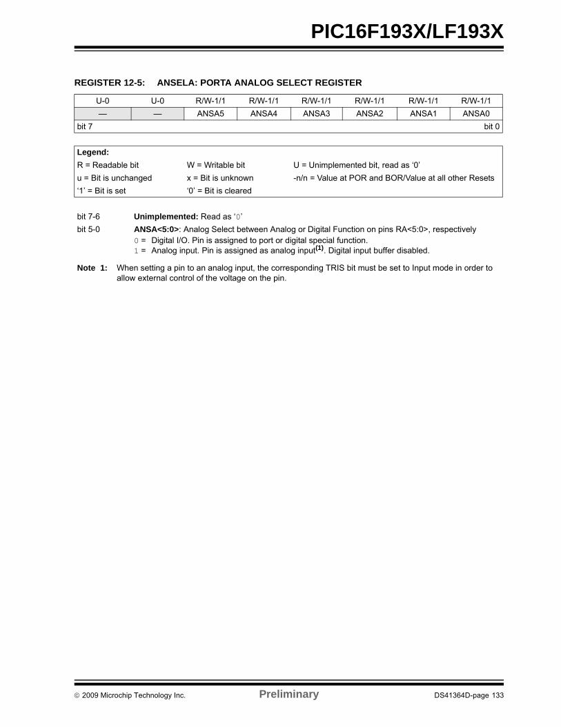
PIC16F193X/LF193X
REGISTER 12-5: ANSELA: PORTA ANALOG SELECT REGISTER
U-0 U-0 R/W-1/1 R/W-1/1 R/W-1/1 R/W-1/1 R/W-1/1 R/W-1/1
— — ANSA5 ANSA4 ANSA3 ANSA2 ANSA1 ANSA0
bit 7 bit 0
Legend:
R = Readable bit W = Writable bit U = Unimplemented bit, read as ‘0’
u = Bit is unchanged x = Bit is unknown -n/n = Value at POR and BOR/Value at all other Resets
‘1’ = Bit is set ‘0’ = Bit is cleared
bit 7-6 Unimplemented: Read as ‘0’
bit 5-0 ANSA<5:0>: Analog Select between Analog or Digital Function on pins RA<5:0>, respectively0 = Digital I/O. Pin is assigned to port or digital special function.1 = Analog input. Pin is assigned as analog input(1). Digital input buffer disabled.
Note 1: When setting a pin to an analog input, the corresponding TRIS bit must be set to Input mode in order to allow external control of the voltage on the pin.
2009 Microchip Technology Inc. Preliminary DS41364D-page 133

PIC16F193X/LF193X
TABLE 12-1: SUMMARY OF REGISTERS ASSOCIATED WITH PORTA
TABLE 12-2: SUMMARY OF CONFIGURATION WORD WITH PORTA
Name Bit 7 Bit 6 Bit 5 Bit 4 Bit 3 Bit 2 Bit 1 Bit 0Register on Page
ADCON0 — CHS<4:0> GO/DONE ADON 161
ADCON1 ADFM ADCS<2:0> — ADNREF ADPREF<1:0> 162
ANSELA — — ANSA5 ANSA4 ANSA3 ANSA2 ANSA1 ANSA0 133
APFCON — CCP3SEL T1GSEL P2BSEL SRNQSEL C2OUTSEL SSSEL CCP2SEL 130
CM1CON0 C1ON C1OUT C1OE C1POL — C1SP C1HYS C1SYNC 180
CM2CON0 C2ON C2OUT C2OE C2POL — C2SP C2HYS C2SYNC 180
CM1CON1 C1NTP C1INTN C1PCH<1:0> — — C1NCH<1:0> 181
CM2CON1 C2NTP C2INTN C2PCH<1:0> — — C2NCH<1:0> 181
CPSCON0 CPSON CPSRM(2) — — CPSRNG<1:0> CPSOUT T0XCS 323
CPSCON1 — — — — CPSCH<3:0> 324
DACCON0 DACEN DACLPS DACOE --- DACPSS<1:0> --- DACNSS 172
LATA LATA7 LATA6 LATA5 LATA4 LATA3 LATA2 LATA1 LATA0 132
LCDCON LCDEN SLPEN WERR — CS<1:0> LMUX<1:0> 329
LCDSE0 SE7 SE6 SE5 SE4 SE3 SE2 SE1 SE0 333
LCDSE1 SE15 SE14 SE13 SE12 SE11 SE10 SE9 SE8 333
OPTION_REG WPUEN INTEDG TMR0CS TMR0SE PSA PS<2:0> 191
PORTA RA7 RA6 RA5 RA4 RA3 RA2 RA1 RA0 132
SRCON0 SRLEN SRCLK<2:0> SRQEN SRNQEN SRPS SRPR 185
SSPxCON1 WCOL SSPxOV SSPxEN CKP SSPxM<3:0> 285
TRISA TRISA7 TRISA6 TRISA5 TRISA4 TRISA3 TRISA2 TRISA1 TRISA0 132
Legend: x = unknown, u = unchanged, – = unimplemented locations read as ‘0’. Shaded cells are not used by PORTA.Note 1: PIC16F193X only.
2: The Capacitive Sensing Reference Mode (CPSRM) bit is not available for the PIC16F/LF1934/1936 devices.
Name Bits Bit -/7 Bit -/6 Bit 13/5 Bit 12/4 Bit 11/3 Bit 10/2 Bit 9/1 Bit 8/0Register on Page
CONFIG113:8 — — FCMEN IESO CLKOUTEN BOREN<1:0> CPD
647:0 CP MCLRE PWRTE WDTE<1:0> FOSC<2:0>
CONFIG213:8 — — LVP DEBUG — BORV STVREN PLLEN
667:0 — — VCAPEN<1:0>(1) — — WRT<1:0>
Legend: — = unimplemented location, read as ‘0’. Shaded cells are not used by PORTA.Note 1: PIC16F193X only.
DS41364D-page 134 Preliminary 2009 Microchip Technology Inc.

PIC16F193X/LF193X
12.3 PORTB Registers
PORTB is an 8-bit wide, bidirectional port. Thecorresponding data direction register is TRISB(Register 12-7). Setting a TRISB bit (= 1) will make thecorresponding PORTB pin an input (i.e., put thecorresponding output driver in a High-Impedance mode).Clearing a TRISB bit (= 0) will make the correspondingPORTB pin an output (i.e., enable the output driver andput the contents of the output latch on the selected pin).Example 12-2 shows how to initialize PORTB.
Reading the PORTB register (Register 12-6) reads thestatus of the pins, whereas writing to it will write to thePORT latch. All write operations are read-modify-writeoperations. Therefore, a write to a port implies that theport pins are read, this value is modified and then writtento the PORT data latch (LATB).
The TRISB register (Register 12-7) controls the PORTBpin output drivers, even when they are being used asanalog inputs. The user should ensure the bits in theTRISB register are maintained set when using them asanalog inputs. I/O pins configured as analog input alwaysread ‘0’.
12.3.1 WEAK PULL-UPS
Each of the PORTB pins has an individually configurableinternal weak pull-up. Control bits WPUB<7:0> enable ordisable each pull-up (see Register 12-10). Each weakpull-up is automatically turned off when the port pin isconfigured as an output. All pull-ups are disabled on aPower-on Reset by the WPUEN bit of the OPTIONregister.
12.3.2 INTERRUPT-ON-CHANGE
All of the PORTB pins are individually configurable as aninterrupt-on-change pin. Control bits IOCB<7:0> enableor disable the interrupt function for each pin. Theinterrupt-on-change feature is disabled on a Power-onReset. Reference Section 13.0“Interrupt-On-Change” for more information.
12.3.3 ANSELB REGISTER
The ANSELB register (Register 12-9) is used toconfigure the Input mode of an I/O pin to analog.Setting the appropriate ANSELB bit high will cause alldigital reads on the pin to be read as ‘0’ and allowanalog functions on the pin to operate correctly.
The state of the ANSELB bits has no affect on digitaloutput functions. A pin with TRIS clear and ANSELB setwill still operate as a digital output, but the Input modewill be analog. This can cause unexpected behaviorwhen executing read-modify-write instructions on theaffected port.
EXAMPLE 12-2: INITIALIZING PORTB
Note: The ANSELB register must be initialized toconfigure an analog channel as a digitalinput. Pins configured as analog inputs willread ‘0’.
BANKSEL PORTB ;CLRF PORTB ;Init PORTBBANKSEL LATB ;Data LatchCLRF LATB ;BANKSEL ANSELBCLRF ANSELB ;Make RB<7:0> digitalBANKSEL TRISB ;MOVLW B’11110000’ ;Set RB<7:4> as inputs
;and RB<3:0> as outputsMOVWF TRISB ;
2009 Microchip Technology Inc. Preliminary DS41364D-page 135

PIC16F193X/LF193X
12.3.4 PORTB FUNCTIONS AND OUTPUT PRIORITIES
Each PORTB pin is multiplexed with other functions. Thepins, their combined functions and their output prioritiesare briefly described here. For additional information,refer to the appropriate section in this data sheet.
When multiple outputs are enabled, the actual pincontrol goes to the peripheral with the lowest number inthe following lists.
Analog input and some digital input functions are notincluded in the list below. These input functions canremain active when the pin is configured as an output.Certain digital input functions, such as the EUSART RXsignal, override other port functions and are included inthe priority list.
RB0
1. SEG0 (LCD)
2. CCP4, 28-pin only
3. RB0
RB1
1. P1C (ECCP1), 28-pin only
2. RB1
RB2
1. P1B (ECCP1), 28-pin only
2. RB2
RB3
1. CCP2/P2A
2. RB3
RB4
1. COM0
2. P1D, 28-pin only
3. RB4
RB5
1. COM1
2. P2B, 28-pin only
3. CCP3/P3A
4. RB5
RB6
1. ICSPCLK (Programming)
2. ICDCLK (enabled by Configuration Word)
3. SEG14 (LCD)
4. RB6
RB7
1. ICSPDAT (Programming)
2. ICDDAT (enabled by Configuration Word)
3. SEG13 (LCD)
4. RB7
REGISTER 12-6: PORTB: PORTB REGISTER
R/W-x/u R/W-x/u R/W-x/u R/W-x/u R/W-x/u R/W-x/u R/W-x/u R/W-x/u
RB7 RB6 RB5 RB4 RB3 RB2 RB1 RB0
bit 7 bit 0
Legend:
R = Readable bit W = Writable bit U = Unimplemented bit, read as ‘0’
u = Bit is unchanged x = Bit is unknown -n/n = Value at POR and BOR/Value at all other Resets
‘1’ = Bit is set ‘0’ = Bit is cleared
bit 7-0 RB<7:0>: PORTB I/O Pin bit1 = Port pin is > VIH
0 = Port pin is < VIL
DS41364D-page 136 Preliminary 2009 Microchip Technology Inc.
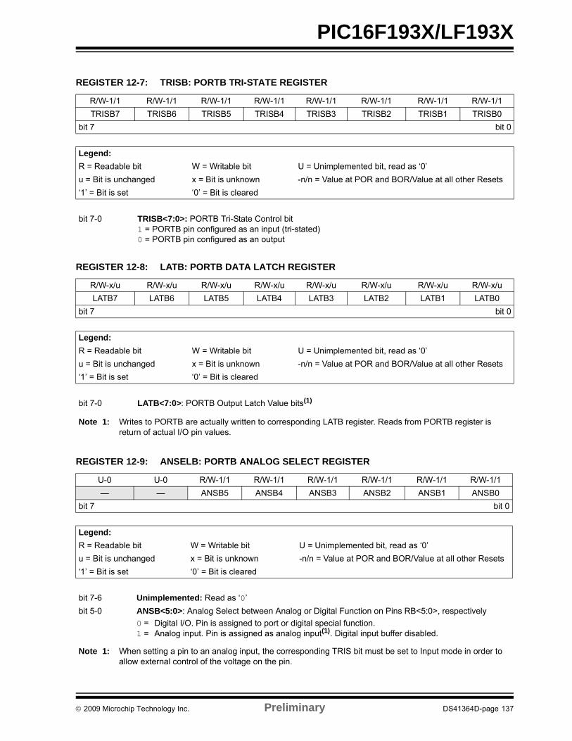
PIC16F193X/LF193X
REGISTER 12-7: TRISB: PORTB TRI-STATE REGISTER
R/W-1/1 R/W-1/1 R/W-1/1 R/W-1/1 R/W-1/1 R/W-1/1 R/W-1/1 R/W-1/1
TRISB7 TRISB6 TRISB5 TRISB4 TRISB3 TRISB2 TRISB1 TRISB0
bit 7 bit 0
Legend:
R = Readable bit W = Writable bit U = Unimplemented bit, read as ‘0’
u = Bit is unchanged x = Bit is unknown -n/n = Value at POR and BOR/Value at all other Resets
‘1’ = Bit is set ‘0’ = Bit is cleared
bit 7-0 TRISB<7:0>: PORTB Tri-State Control bit1 = PORTB pin configured as an input (tri-stated)0 = PORTB pin configured as an output
REGISTER 12-8: LATB: PORTB DATA LATCH REGISTER
R/W-x/u R/W-x/u R/W-x/u R/W-x/u R/W-x/u R/W-x/u R/W-x/u R/W-x/u
LATB7 LATB6 LATB5 LATB4 LATB3 LATB2 LATB1 LATB0
bit 7 bit 0
Legend:
R = Readable bit W = Writable bit U = Unimplemented bit, read as ‘0’
u = Bit is unchanged x = Bit is unknown -n/n = Value at POR and BOR/Value at all other Resets
‘1’ = Bit is set ‘0’ = Bit is cleared
bit 7-0 LATB<7:0>: PORTB Output Latch Value bits(1)
Note 1: Writes to PORTB are actually written to corresponding LATB register. Reads from PORTB register is return of actual I/O pin values.
REGISTER 12-9: ANSELB: PORTB ANALOG SELECT REGISTER
U-0 U-0 R/W-1/1 R/W-1/1 R/W-1/1 R/W-1/1 R/W-1/1 R/W-1/1
— — ANSB5 ANSB4 ANSB3 ANSB2 ANSB1 ANSB0
bit 7 bit 0
Legend:
R = Readable bit W = Writable bit U = Unimplemented bit, read as ‘0’
u = Bit is unchanged x = Bit is unknown -n/n = Value at POR and BOR/Value at all other Resets
‘1’ = Bit is set ‘0’ = Bit is cleared
bit 7-6 Unimplemented: Read as ‘0’
bit 5-0 ANSB<5:0>: Analog Select between Analog or Digital Function on Pins RB<5:0>, respectively
0 = Digital I/O. Pin is assigned to port or digital special function.1 = Analog input. Pin is assigned as analog input(1). Digital input buffer disabled.
Note 1: When setting a pin to an analog input, the corresponding TRIS bit must be set to Input mode in order to allow external control of the voltage on the pin.
2009 Microchip Technology Inc. Preliminary DS41364D-page 137
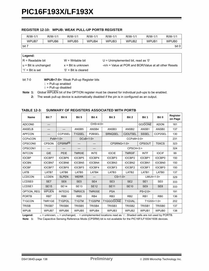
PIC16F193X/LF193X
TABLE 12-3: SUMMARY OF REGISTERS ASSOCIATED WITH PORTB
REGISTER 12-10: WPUB: WEAK PULL-UP PORTB REGISTER
R/W-1/1 R/W-1/1 R/W-1/1 R/W-1/1 R/W-1/1 R/W-1/1 R/W-1/1 R/W-1/1
WPUB7 WPUB6 WPUB5 WPUB4 WPUB3 WPUB2 WPUB1 WPUB0
bit 7 bit 0
Legend:
R = Readable bit W = Writable bit U = Unimplemented bit, read as ‘0’
u = Bit is unchanged x = Bit is unknown -n/n = Value at POR and BOR/Value at all other Resets
‘1’ = Bit is set ‘0’ = Bit is cleared
bit 7-0 WPUB<7:0>: Weak Pull-up Register bits1 = Pull-up enabled0 = Pull-up disabled
Note 1: Global WPUEN bit of the OPTION register must be cleared for individual pull-ups to be enabled.
2: The weak pull-up device is automatically disabled if the pin is in configured as an output.
Name Bit 7 Bit 6 Bit 5 Bit 4 Bit 3 Bit 2 Bit 1 Bit 0Register on Page
ADCON0 — CHS<4:0> GO/DONE ADON 161
ANSELB — — ANSB5 ANSB4 ANSB3 ANSB2 ANSB1 ANSB0 137
APFCON — CCP3SEL T1GSEL P2BSEL SRNQSEL C2OUTSEL SSSEL CCP2SEL 130
CCPxCON PxM<1:0> DCxB<1:0> CCPxM<3:0> 231
CPSCON0 CPSON CPSRM(1) — — CPSRNG<1:0> CPSOUT T0XCS 323
CPSCON1 — — — — CPSCH<3:> 324
INTCON GIE PEIE TMR0IE INTE IOCIE TMR0IF INTF IOCIF 99
IOCBP IOCBP7 IOCBP6 IOCBP5 IOCBP4 IOCBP3 IOCBP2 IOCBP1 IOCBP0 150
IOCBN IOCBN7 IOCBN6 IOCBN5 IOCBN4 IOCBN3 IOCBN2 IOCBN1 IOCBN0 150
IOCBF IOCBF7 IOCBF6 IOCBF5 IOCBF4 IOCBF3 IOCBF2 IOCBF1 IOCBF0 150
LATB LATB7 LATB6 LATB5 LATB4 LATB3 LATB2 LATB1 LATB0 137
LCDCON LCDEN SLPEN WERR — CS<1:0> LMUX<1:0> 329
LCDSE0 SE7 SE6 SE5 SE4 SE3 SE2 SE1 SE0 333
LCDSE1 SE15 SE14 SE13 SE12 SE11 SE10 SE9 SE8 333
OPTION_REG WPUEN INTEDG TMR0CS TMR0SE PSA PS<2:0> 191
PORTB RB7 RB6 RB5 RB4 RB3 RB2 RB1 RB0 136
T1GCON TMR1GE T1GPOL T1GTM T1GSPM T1GGO/DONE T1GVAL T1GSS<1:0> 202
TRISB TRISB7 TRISB6 TRISB5 TRISB4 TRISB3 TRISB2 TRISB1 TRISB0 137
WPUB WPUB7 WPUB6 WPUB5 WPUB4 WPUB3 WPUB2 WPUB1 WPUB0 138
Legend: x = unknown, u = unchanged, - = unimplemented locations read as ‘0’. Shaded cells are not used by PORTB.Note 1: The Capacitive Sensing Reference Mode (CPSRM) bit is not available for the PIC16F/LF1934/1936 devices.
DS41364D-page 138 Preliminary 2009 Microchip Technology Inc.

PIC16F193X/LF193X
12.4 PORTC Registers
PORTC is a 8-bit wide, bidirectional port. Thecorresponding data direction register is TRISC(Register 12-12). Setting a TRISC bit (= 1) will make thecorresponding PORTC pin an input (i.e., put thecorresponding output driver in a High-Impedance mode).Clearing a TRISC bit (= 0) will make the correspondingPORTC pin an output (i.e., enable the output driver andput the contents of the output latch on the selected pin).Example 12-3 shows how to initialize PORTC.
Reading the PORTC register (Register 12-11) reads thestatus of the pins, whereas writing to it will write to thePORT latch. All write operations are read-modify-writeoperations. Therefore, a write to a port implies that theport pins are read, this value is modified and then writtento the PORT data latch (LATC).
The TRISC register (Register 12-12) controls thePORTC pin output drivers, even when they are beingused as analog inputs. The user should ensure the bits inthe TRISC register are maintained set when using themas analog inputs. I/O pins configured as analog inputalways read ‘0’.
EXAMPLE 12-3: INITIALIZING PORTC
12.4.1 PORTC FUNCTIONS AND OUTPUT PRIORITIES
Each PORTC pin is multiplexed with other functions. Thepins, their combined functions and their output prioritiesare briefly described here. For additional information,refer to the appropriate section in this data sheet.
When multiple outputs are enabled, the actual pincontrol goes to the peripheral with the lowest number inthe following lists.
Analog input and some digital input functions are notincluded in the list below. These input functions canremain active when the pin is configured as an output.Certain digital input functions override other portfunctions and are included in the priority list.
RC0
1. T1OSO (Timer1 Oscillator)
2. CCP2/P2B
3. RC0
RC1
1. T1OSI (Timer1 Oscillator)
2. CCP2/P2A
3. RC1
RC2
1. SEG3 (LCD)
2. CCP1/P1A
3. RC2
RC3
1. SEG6 (LCD)
2. SCL (MSSP)
3. SCK (MSSP)
4. RC3
RC4
1. SEG11 (LCD)
2. SDA (MSSP)
3. RC4
RC5
1. SEG10 (LCD)
2. SDO (MSSP)
3. RC5
RC6
1. SEG9 (LCD)
2. TX (EUSART)
3. CK (EUSART)
4. CCP3/P3A, 28-pin only
5. RC6
RC7
1. SEG8 (LCD)
2. DT (EUSART)
3. CCP3/P3B, 28 pin only
4. RC7
BANKSEL PORTC ;CLRF PORTC ;Init PORTCBANKSEL LATC ;Data LatchCLRF LATC ;BANKSEL ANSELC ;CLRF ANSELC ;digital I/OBANKSEL TRISC ;MOVLW B'11110000' ;Set RC<7:4> as inputsMOVWF TRISC ;and set RC<3:0> as
;outputs
2009 Microchip Technology Inc. Preliminary DS41364D-page 139

PIC16F193X/LF193X
REGISTER 12-11: PORTC: PORTC REGISTER
R/W-x/u R/W-x/u R/W-x/u R/W-x/u R/W-x/u R/W-x/u R/W-x/u R/W-x/u
RC7 RC6 RC5 RC4 RC3 RC2 RC1 RC0
bit 7 bit 0
Legend:
R = Readable bit W = Writable bit U = Unimplemented bit, read as ‘0’
u = Bit is unchanged x = Bit is unknown -n/n = Value at POR and BOR/Value at all other Resets
‘1’ = Bit is set ‘0’ = Bit is cleared
bit 7-0 RC<7:0>: PORTC General Purpose I/O Pin bits1 = Port pin is > VIH
0 = Port pin is < VIL
REGISTER 12-12: TRISC: PORTC TRI-STATE REGISTER
R/W-1/1 R/W-1/1 R/W-1/1 R/W-1/1 R/W-1/1 R/W-1/1 R/W-1/1 R/W-1/1
TRISC7 TRISC6 TRISC5 TRISC4 TRISC3 TRISC2 TRISC1 TRISC0
bit 7 bit 0
Legend:
R = Readable bit W = Writable bit U = Unimplemented bit, read as ‘0’
u = Bit is unchanged x = Bit is unknown -n/n = Value at POR and BOR/Value at all other Resets
‘1’ = Bit is set ‘0’ = Bit is cleared
bit 7-0 TRISC<7:0>: PORTC Tri-State Control bits1 = PORTC pin configured as an input (tri-stated)0 = PORTC pin configured as an output
REGISTER 12-13: LATC: PORTC DATA LATCH REGISTER
R/W-x/u R/W-x/u R/W-x/u R/W-x/u R/W-x/u R/W-x/u R/W-x/u R/W-x/u
LATC7 LATC6 LATC5 LATC4 LATC3 LATC2 LATC1 LATC0
bit 7 bit 0
Legend:
R = Readable bit W = Writable bit U = Unimplemented bit, read as ‘0’
u = Bit is unchanged x = Bit is unknown -n/n = Value at POR and BOR/Value at all other Resets
‘1’ = Bit is set ‘0’ = Bit is cleared
bit 7-0 LATC<7:0>: PORTC Output Latch Value bits(1)
Note 1: Writes to PORTC are actually written to corresponding LATC register. Reads from PORTC register is return of actual I/O pin values.
DS41364D-page 140 Preliminary 2009 Microchip Technology Inc.
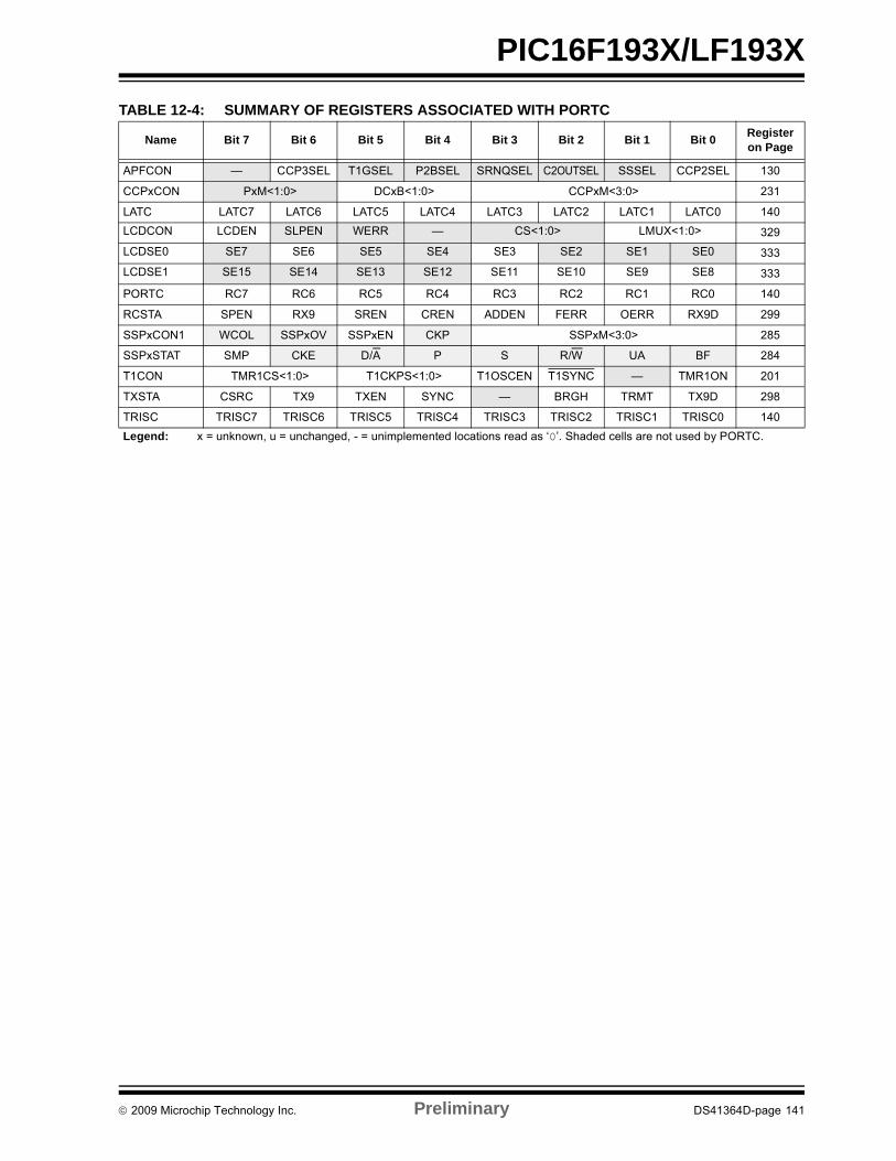
PIC16F193X/LF193X
TABLE 12-4: SUMMARY OF REGISTERS ASSOCIATED WITH PORTC
Name Bit 7 Bit 6 Bit 5 Bit 4 Bit 3 Bit 2 Bit 1 Bit 0Register on Page
APFCON — CCP3SEL T1GSEL P2BSEL SRNQSEL C2OUTSEL SSSEL CCP2SEL 130
CCPxCON PxM<1:0> DCxB<1:0> CCPxM<3:0> 231
LATC LATC7 LATC6 LATC5 LATC4 LATC3 LATC2 LATC1 LATC0 140
LCDCON LCDEN SLPEN WERR — CS<1:0> LMUX<1:0> 329
LCDSE0 SE7 SE6 SE5 SE4 SE3 SE2 SE1 SE0 333
LCDSE1 SE15 SE14 SE13 SE12 SE11 SE10 SE9 SE8 333
PORTC RC7 RC6 RC5 RC4 RC3 RC2 RC1 RC0 140
RCSTA SPEN RX9 SREN CREN ADDEN FERR OERR RX9D 299
SSPxCON1 WCOL SSPxOV SSPxEN CKP SSPxM<3:0> 285
SSPxSTAT SMP CKE D/A P S R/W UA BF 284
T1CON TMR1CS<1:0> T1CKPS<1:0> T1OSCEN T1SYNC — TMR1ON 201
TXSTA CSRC TX9 TXEN SYNC — BRGH TRMT TX9D 298
TRISC TRISC7 TRISC6 TRISC5 TRISC4 TRISC3 TRISC2 TRISC1 TRISC0 140
Legend: x = unknown, u = unchanged, - = unimplemented locations read as ‘0’. Shaded cells are not used by PORTC.
2009 Microchip Technology Inc. Preliminary DS41364D-page 141

PIC16F193X/LF193X
12.5 PORTD Registers
PORTD is a 8-bit wide, bidirectional port. Thecorresponding data direction register is TRISD(Register 12-14). Setting a TRISD bit (= 1) will make thecorresponding PORTD pin an input (i.e., put thecorresponding output driver in a High-Impedance mode).Clearing a TRISD bit (= 0) will make the correspondingPORTD pin an output (i.e., enable the output driver andput the contents of the output latch on the selected pin).Example 12-4 shows how to initialize PORTD.
Reading the PORTD register (Register 12-14) reads thestatus of the pins, whereas writing to it will write to thePORT latch. All write operations are read-modify-writeoperations. Therefore, a write to a port implies that theport pins are read, this value is modified and then writtento the PORT data latch (LATD).
The TRISD register (Register 12-15) controls thePORTD pin output drivers, even when they are beingused as analog inputs. The user should ensure the bitsin the TRISD register are maintained set when usingthem as analog inputs. I/O pins configured as analoginput always read ‘0’.
12.5.1 ANSELD REGISTER
The ANSELD register (Register 12-17) is used toconfigure the Input mode of an I/O pin to analog.Setting the appropriate ANSELD bit high will cause alldigital reads on the pin to be read as ‘0’ and allowanalog functions on the pin to operate correctly.
The state of the ANSELD bits has no affect on digitaloutput functions. A pin with TRIS clear and ANSEL setwill still operate as a digital output, but the Input modewill be analog. This can cause unexpected behaviorwhen executing read-modify-write instructions on theaffected port.
EXAMPLE 12-4: INITIALIZING PORTD
12.5.2 PORTD FUNCTIONS AND OUTPUT PRIORITIES
Each PORTD pin is multiplexed with other functions. Thepins, their combined functions and their output prioritiesare briefly described here. For additional information,refer to the appropriate section in this data sheet.
When multiple outputs are enabled, the actual pincontrol goes to the peripheral with the lowest number inthe following lists.
Analog input and some digital input functions are notincluded in the list below. These input functions canremain active when the pin is configured as an output.Certain digital input functions override other portfunctions and are included in the priority list.
RD0
1. COM3 (LCD)
2. RD0
RD1
1. CCP4 (CCP)
2. RD1
RD2
1. P2B (CCP)
2. RD2
RD3
1. SEG16 (LCD)
2. P2C (CCP)
3. RD3
RD4
1. SEG17 (LCD)
2. P2D (CCP)
3. RD4
RD5
1. SEG18 (LCD)
2. P1B (CCP)
3. RD5
RD6
1. SEG19 (LCD)
2. P1C (CCP)
3. RD6
RD7
1. SEG20 (LCD)
2. P1D (CCP)
3. RD7
Note: PORTD is available on PIC16F1936 andPIC16F1938 only.
Note: The ANSELD register must be initializedto configure an analog channel as a digitalinput. Pins configured as analog inputs willread ‘0’.
BANKSEL PORTD ;CLRF PORTD ;Init PORTDBANKSEL LATD ;Data LatchCLRF LATD ;BANKSEL ANSELD ;CLRF ANSELD ;digital I/OBANKSEL TRISD ;MOVLW B'11110000' ;Set RD<7:4> as inputsMOVWF TRISD ;and set RD<3:0> as
;outputs
DS41364D-page 142 Preliminary 2009 Microchip Technology Inc.
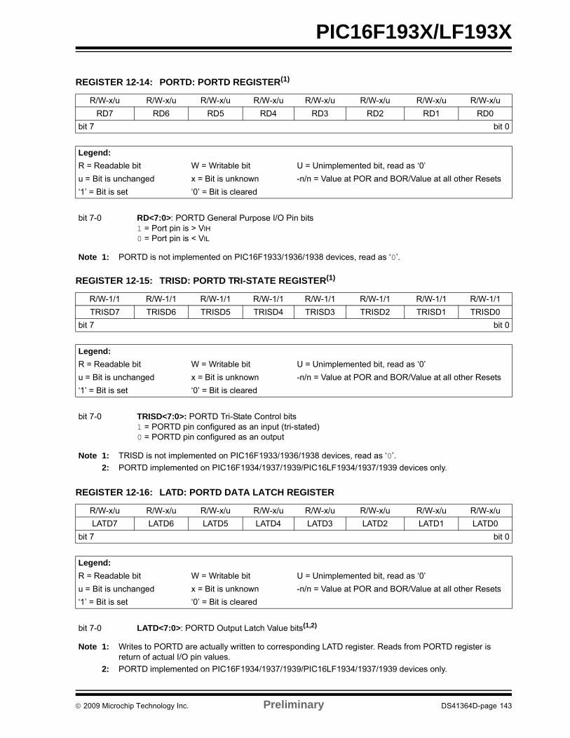
PIC16F193X/LF193X
REGISTER 12-14: PORTD: PORTD REGISTER(1)
R/W-x/u R/W-x/u R/W-x/u R/W-x/u R/W-x/u R/W-x/u R/W-x/u R/W-x/u
RD7 RD6 RD5 RD4 RD3 RD2 RD1 RD0
bit 7 bit 0
Legend:
R = Readable bit W = Writable bit U = Unimplemented bit, read as ‘0’
u = Bit is unchanged x = Bit is unknown -n/n = Value at POR and BOR/Value at all other Resets
‘1’ = Bit is set ‘0’ = Bit is cleared
bit 7-0 RD<7:0>: PORTD General Purpose I/O Pin bits1 = Port pin is > VIH
0 = Port pin is < VIL
Note 1: PORTD is not implemented on PIC16F1933/1936/1938 devices, read as ‘0’.
REGISTER 12-15: TRISD: PORTD TRI-STATE REGISTER(1)
R/W-1/1 R/W-1/1 R/W-1/1 R/W-1/1 R/W-1/1 R/W-1/1 R/W-1/1 R/W-1/1
TRISD7 TRISD6 TRISD5 TRISD4 TRISD3 TRISD2 TRISD1 TRISD0
bit 7 bit 0
Legend:
R = Readable bit W = Writable bit U = Unimplemented bit, read as ‘0’
u = Bit is unchanged x = Bit is unknown -n/n = Value at POR and BOR/Value at all other Resets
‘1’ = Bit is set ‘0’ = Bit is cleared
bit 7-0 TRISD<7:0>: PORTD Tri-State Control bits1 = PORTD pin configured as an input (tri-stated)0 = PORTD pin configured as an output
Note 1: TRISD is not implemented on PIC16F1933/1936/1938 devices, read as ‘0’.
2: PORTD implemented on PIC16F1934/1937/1939/PIC16LF1934/1937/1939 devices only.
REGISTER 12-16: LATD: PORTD DATA LATCH REGISTER
R/W-x/u R/W-x/u R/W-x/u R/W-x/u R/W-x/u R/W-x/u R/W-x/u R/W-x/u
LATD7 LATD6 LATD5 LATD4 LATD3 LATD2 LATD1 LATD0
bit 7 bit 0
Legend:
R = Readable bit W = Writable bit U = Unimplemented bit, read as ‘0’
u = Bit is unchanged x = Bit is unknown -n/n = Value at POR and BOR/Value at all other Resets
‘1’ = Bit is set ‘0’ = Bit is cleared
bit 7-0 LATD<7:0>: PORTD Output Latch Value bits(1,2)
Note 1: Writes to PORTD are actually written to corresponding LATD register. Reads from PORTD register is return of actual I/O pin values.
2: PORTD implemented on PIC16F1934/1937/1939/PIC16LF1934/1937/1939 devices only.
2009 Microchip Technology Inc. Preliminary DS41364D-page 143

PIC16F193X/LF193X
TABLE 12-5: SUMMARY OF REGISTERS ASSOCIATED WITH PORTD(1)
REGISTER 12-17: ANSELD: PORTD ANALOG SELECT REGISTER(2)
R/W-1/1 R/W-1/1 R/W-1/1 R/W-1/1 R/W-1/1 R/W-1/1 R/W-1/1 R/W-1/1
ANSD7 ANSD6 ANSD5 ANSD4 ANSD3 ANSD2 ANSD1 ANSD0
bit 7 bit 0
Legend:
R = Readable bit W = Writable bit U = Unimplemented bit, read as ‘0’
u = Bit is unchanged x = Bit is unknown -n/n = Value at POR and BOR/Value at all other Resets
‘1’ = Bit is set ‘0’ = Bit is cleared
bit 7-0 ANSD<7:0>: Analog Select between Analog or Digital Function on Pins RD<7:0>, respectively
0 = Digital I/O. Pin is assigned to port or digital special function.1 = Analog input. Pin is assigned as analog input(1). Digital input buffer disabled.
Note 1: When setting a pin to an analog input, the corresponding TRIS bit must be set to Input mode in order to allow external control of the voltage on the pin.
2: ANSELD register is not implemented on the PIC16F1933/1936/1938. Read as ‘0’.
3: PORTD implemented on PIC16F1934/1937/1939/PIC16LF1934/1937/1939 devices only.
Name Bit 7 Bit 6 Bit 5 Bit 4 Bit 3 Bit 2 Bit 1 Bit 0Register on
Page
ANSELD ANSD7 ANSD6 ANSD5 ANSD4 ANSD3 ANSD2 ANSD1 ANSD0 144
CCPxCON PxM<1:0> DCxB<1:0> CCPxM<3:0> 231
CPSCON0 CPSON CPSRM(2) — — CPSRNG<1:0> CPSOUT T0XCS 323
CPSCON1 — — — — CPSCH<3:0> 324
LATD LATD7 LATD6 LATD5 LATD4 LATD3 LATD2 LATD1 LATD0 143
LCDCON LCDEN SLPEN WERR — CS<1:0> LMUX<1:0> 329
LCDSE2 SE23 SE22 SE21 SE20 SE19 SE18 SE17 SE16 333
PORTD RD7 RD6 RD5 RD4 RD3 RD2 RD1 RD0 143
TRISD TRISD7 TRISD6 TRISD5 TRISD4 TRISD3 TRISD2 TRISD1 TRISD0 143
Legend: x = unknown, u = unchanged, – = unimplemented locations read as ‘0’. Shaded cells are not used by PORTD.Note 1: These registers are not implemented on the PIC16F1933/1936/1938 devices, read as ‘0’.
2: The Capacitive Sensing Reference Mode (CPSRM) bit is not available for the PIC16F/LF1934/1936 devices.
DS41364D-page 144 Preliminary 2009 Microchip Technology Inc.

PIC16F193X/LF193X
12.6 PORTE Registers
PORTE is a 4-bit wide, bidirectional port. Thecorresponding data direction register is TRISE. Setting aTRISE bit (= 1) will make the corresponding PORTE pinan input (i.e., put the corresponding output driver in aHigh-Impedance mode). Clearing a TRISE bit (= 0) willmake the corresponding PORTE pin an output (i.e.,enable the output driver and put the contents of theoutput latch on the selected pin). The exception is RE3,which is input only and its TRIS bit will always read as‘1’. Example 12-5 shows how to initialize PORTE.
Reading the PORTE register (Register 12-18) readsthe status of the pins, whereas writing to it will write tothe PORT latch. All write operations areread-modify-write operations. Therefore, a write to aport implies that the port pins are read, this value ismodified and then written to the PORT data latch(LATE). RE3 reads ‘0’ when MCLRE = 1.
12.6.1 ANSELE REGISTER
The ANSELE register (Register 12-21) is used toconfigure the Input mode of an I/O pin to analog.Setting the appropriate ANSELE bit high will cause alldigital reads on the pin to be read as ‘0’ and allowanalog functions on the pin to operate correctly.
The state of the ANSELE bits has no affect on digitaloutput functions. A pin with TRIS clear and ANSEL setwill still operate as a digital output, but the Input modewill be analog. This can cause unexpected behaviorwhen executing read-modify-write instructions on theaffected port.
The TRISE register (Register 12-19) controls the PORTEpin output drivers, even when they are being used asanalog inputs. The user should ensure the bits in theTRISE register are maintained set when using them asanalog inputs. I/O pins configured as analog input alwaysread ‘0’.
EXAMPLE 12-5: INITIALIZING PORTE
12.6.2 PORTE FUNCTIONS AND OUTPUT PRIORITIES
Each PORTE pin is multiplexed with other functions. Thepins, their combined functions and their output prioritiesare briefly described here. For additional information,refer to the appropriate section in this data sheet.
When multiple outputs are enabled, the actual pincontrol goes to the peripheral with the lowest number inthe following lists.
Analog input and some digital input functions are notincluded in the list below. These input functions canremain active when the pin is configured as an output.Certain digital input functions, such as the EUSART RXsignal, override other port functions and are included inthe priority list.
RE0
1. SEG21 (LCD)
2. CCP3/P3A (CCP)
3. RE0
RE1
1. SEG22 (LCD)
2. P3B (CCP)
3. RE1
RE2
1. SEG23 (LCD)
2. CCP5 (CCP)
3. RE2
Note: RE<2:0> and TRISE<2:0> pins areavailable on PIC16F1936 and PIC16F1938only.
Note: The ANSELE register must be initialized toconfigure an analog channel as a digitalinput. Pins configured as analog inputs willread ‘0’.
BANKSEL PORTE ;CLRF PORTE ;Init PORTEBANKSEL LATE ;Data LatchCLRF LATE ;BANKSEL ANSELE ;CLRF ANSELE ;digital I/OBANKSEL TRISE ;MOVLW B‘00001100’ ;Set RE<3:2> as inputsMOVWF TRISE ;and set RE<1:0>
;as outputs
2009 Microchip Technology Inc. Preliminary DS41364D-page 145
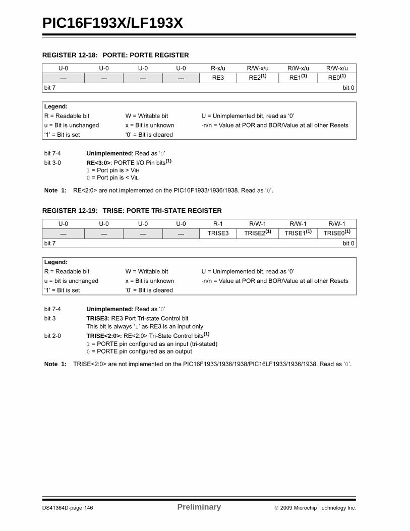
PIC16F193X/LF193X
REGISTER 12-18: PORTE: PORTE REGISTER
U-0 U-0 U-0 U-0 R-x/u R/W-x/u R/W-x/u R/W-x/u
— — — — RE3 RE2(1) RE1(1) RE0(1)
bit 7 bit 0
Legend:
R = Readable bit W = Writable bit U = Unimplemented bit, read as ‘0’
u = Bit is unchanged x = Bit is unknown -n/n = Value at POR and BOR/Value at all other Resets
‘1’ = Bit is set ‘0’ = Bit is cleared
bit 7-4 Unimplemented: Read as ‘0’
bit 3-0 RE<3:0>: PORTE I/O Pin bits(1)
1 = Port pin is > VIH
0 = Port pin is < VIL
Note 1: RE<2:0> are not implemented on the PIC16F1933/1936/1938. Read as ‘0’.
REGISTER 12-19: TRISE: PORTE TRI-STATE REGISTER
U-0 U-0 U-0 U-0 R-1 R/W-1 R/W-1 R/W-1
— — — — TRISE3 TRISE2(1) TRISE1(1) TRISE0(1)
bit 7 bit 0
Legend:
R = Readable bit W = Writable bit U = Unimplemented bit, read as ‘0’
u = bit is unchanged x = Bit is unknown -n/n = Value at POR and BOR/Value at all other Resets
‘1’ = Bit is set ‘0’ = Bit is cleared
bit 7-4 Unimplemented: Read as ‘0’
bit 3 TRISE3: RE3 Port Tri-state Control bitThis bit is always ‘1’ as RE3 is an input only
bit 2-0 TRISE<2:0>: RE<2:0> Tri-State Control bits(1)
1 = PORTE pin configured as an input (tri-stated)0 = PORTE pin configured as an output
Note 1: TRISE<2:0> are not implemented on the PIC16F1933/1936/1938/PIC16LF1933/1936/1938. Read as ‘0’.
DS41364D-page 146 Preliminary 2009 Microchip Technology Inc.

PIC16F193X/LF193X
REGISTER 12-20: LATE: PORTE DATA LATCH REGISTER
U-0 U-0 U-0 U-0 R/W-x/u R/W-x/u R/W-x/u R/W-x/u
— — — — LATE3 LATE2 LATE1 LATE0
bit 7 bit 0
Legend:
R = Readable bit W = Writable bit U = Unimplemented bit, read as ‘0’
u = Bit is unchanged x = Bit is unknown -n/n = Value at POR and BOR/Value at all other Resets
‘1’ = Bit is set ‘0’ = Bit is cleared
bit 7-4 Unimplemented: Read as ‘0’
bit 3-0 LATE<3:0>: PORTE Output Latch Value bits(1)
Note 1: Writes to PORTE are actually written to corresponding LATE register. Reads from PORTE register is return of actual I/O pin values.
REGISTER 12-21: ANSELE: PORTE ANALOG SELECT REGISTER
U-0 U-0 U-0 U-0 U-0 R/W-1 R/W-1 R/W-1
— — — — — ANSE2(2) ANSE1(2) ANSE0(2)
bit 7 bit 0
Legend:
R = Readable bit W = Writable bit U = Unimplemented bit, read as ‘0’
u = bit is unchanged x = Bit is unknown -n/n = Value at POR and BOR/Value at all other Resets
‘1’ = Bit is set ‘0’ = Bit is cleared
bit 7-3 Unimplemented: Read as ‘0’
bit 2-0 ANSE<2:0>: Analog Select between Analog or Digital Function on Pins RE<2:0>, respectively0 = Digital I/O. Pin is assigned to port or digital special function.1 = Analog input. Pin is assigned as analog input(1). Digital input buffer disabled.
Note 1: When setting a pin to an analog input, the corresponding TRIS bit must be set to Input mode in order to allow external control of the voltage on the pin.
2: ANSELE register is not implemented on the PIC16F1933/1936/1938/PIC16LF1933/1936/1938. Read as ‘0’
2009 Microchip Technology Inc. Preliminary DS41364D-page 147
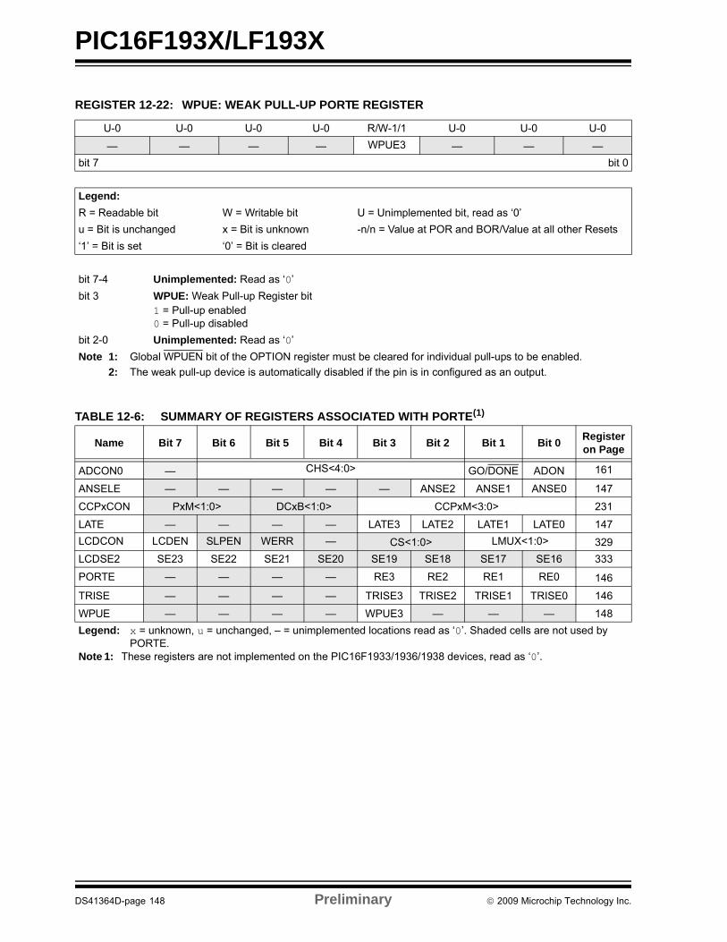
PIC16F193X/LF193X
TABLE 12-6: SUMMARY OF REGISTERS ASSOCIATED WITH PORTE(1)
REGISTER 12-22: WPUE: WEAK PULL-UP PORTE REGISTER
U-0 U-0 U-0 U-0 R/W-1/1 U-0 U-0 U-0
— — — — WPUE3 — — —
bit 7 bit 0
Legend:
R = Readable bit W = Writable bit U = Unimplemented bit, read as ‘0’
u = Bit is unchanged x = Bit is unknown -n/n = Value at POR and BOR/Value at all other Resets
‘1’ = Bit is set ‘0’ = Bit is cleared
bit 7-4 Unimplemented: Read as ‘0’
bit 3 WPUE: Weak Pull-up Register bit1 = Pull-up enabled0 = Pull-up disabled
bit 2-0 Unimplemented: Read as ‘0’
Note 1: Global WPUEN bit of the OPTION register must be cleared for individual pull-ups to be enabled.
2: The weak pull-up device is automatically disabled if the pin is in configured as an output.
Name Bit 7 Bit 6 Bit 5 Bit 4 Bit 3 Bit 2 Bit 1 Bit 0Register on Page
ADCON0 — CHS<4:0> GO/DONE ADON 161
ANSELE — — — — — ANSE2 ANSE1 ANSE0 147
CCPxCON PxM<1:0> DCxB<1:0> CCPxM<3:0> 231
LATE — — — — LATE3 LATE2 LATE1 LATE0 147
LCDCON LCDEN SLPEN WERR — CS<1:0> LMUX<1:0> 329
LCDSE2 SE23 SE22 SE21 SE20 SE19 SE18 SE17 SE16 333
PORTE — — — — RE3 RE2 RE1 RE0 146
TRISE — — — — TRISE3 TRISE2 TRISE1 TRISE0 146
WPUE — — — — WPUE3 — — — 148
Legend: x = unknown, u = unchanged, – = unimplemented locations read as ‘0’. Shaded cells are not used by PORTE.
Note 1: These registers are not implemented on the PIC16F1933/1936/1938 devices, read as ‘0’.
DS41364D-page 148 Preliminary 2009 Microchip Technology Inc.
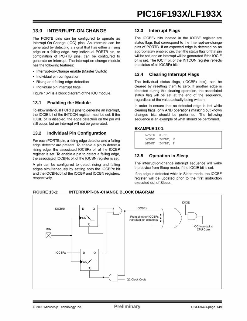
PIC16F193X/LF193X
13.0 INTERRUPT-ON-CHANGE
The PORTB pins can be configured to operate asInterrupt-On-Change (IOC) pins. An interrupt can begenerated by detecting a signal that has either a risingedge or a falling edge. Any individual PORTB pin, orcombination of PORTB pins, can be configured togenerate an interrupt. The interrupt-on-change modulehas the following features:
• Interrupt-on-Change enable (Master Switch)
• Individual pin configuration
• Rising and falling edge detection
• Individual pin interrupt flags
Figure 13-1 is a block diagram of the IOC module.
13.1 Enabling the Module
To allow individual PORTB pins to generate an interrupt,the IOCIE bit of the INTCON register must be set. If theIOCIE bit is disabled, the edge detection on the pin willstill occur, but an interrupt will not be generated.
13.2 Individual Pin Configuration
For each PORTB pin, a rising edge detector and a fallingedge detector are present. To enable a pin to detect arising edge, the associated IOCBPx bit of the IOCBPregister is set. To enable a pin to detect a falling edge,the associated IOCBNx bit of the IOCBN register is set.
A pin can be configured to detect rising and fallingedges simultaneously by setting both the IOCBPx bitand the IOCBNx bit of the IOCBP and IOCBN registers,respectively.
13.3 Interrupt Flags
The IOCBFx bits located in the IOCBF register arestatus flags that correspond to the Interrupt-on-changepins of PORTB. If an expected edge is detected on anappropriately enabled pin, then the status flag for that pinwill be set, and an interrupt will be generated if the IOCIEbit is set. The IOCIF bit of the INTCON register reflectsthe status of all IOCBFx bits.
13.4 Clearing Interrupt Flags
The individual status flags, (IOCBFx bits), can becleared by resetting them to zero. If another edge isdetected during this clearing operation, the associatedstatus flag will be set at the end of the sequence,regardless of the value actually being written.
In order to ensure that no detected edge is lost whileclearing flags, only AND operations masking out knownchanged bits should be performed. The followingsequence is an example of what should be performed.
EXAMPLE 13-1:
13.5 Operation in Sleep
The interrupt-on-change interrupt sequence will wakethe device from Sleep mode, if the IOCIE bit is set.
If an edge is detected while in Sleep mode, the IOCBFregister will be updated prior to the first instructionexecuted out of Sleep.
FIGURE 13-1: INTERRUPT-ON-CHANGE BLOCK DIAGRAM
MOVLW 0xffXORWF IOCBF, WANDWF IOCBF, F
RBx
From all other IOCBFxindividual pin detectors
D Q
CK
R
D Q
CK
R
IOCBNx
IOCBPx
Q2 Clock Cycle
IOCIE
IOC Interrupt toCPU Core
IOCBFx
2009 Microchip Technology Inc. Preliminary DS41364D-page 149

PIC16F193X/LF193X
REGISTER 13-1: IOCBP: INTERRUPT-ON-CHANGE POSITIVE EDGE REGISTER
R/W-0/0 R/W-0/0 R/W-0/0 R/W-0/0 R/W-0/0 R/W-0/0 R/W-0/0 R/W-0/0
IOCBP7 IOCBP6 IOCBP5 IOCBP4 IOCBP3 IOCBP2 IOCBP1 IOCBP0
bit 7 bit 0
Legend:
R = Readable bit W = Writable bit U = Unimplemented bit, read as ‘0’
u = Bit is unchanged x = Bit is unknown -n/n = Value at POR and BOR/Value at all other Resets
‘1’ = Bit is set ‘0’ = Bit is cleared
bit 7-0 IOCBP<7:0>: Interrupt-on-Change Positive Edge Enable bits
1 = Interrupt-on-Change enabled on the pin for a positive going edge. Associated Status bit andinterrupt flag will be set upon detecting an edge.
0 = Interrupt-on-Change disabled for the associated pin.
REGISTER 13-2: IOCBN: INTERRUPT-ON-CHANGE NEGATIVE EDGE REGISTER
R/W-0/0 R/W-0/0 R/W-0/0 R/W-0/0 R/W-0/0 R/W-0/0 R/W-0/0 R/W-0/0
IOCBN7 IOCBN6 IOCBN5 IOCBN4 IOCBN3 IOCBN2 IOCBN1 IOCBN0
bit 7 bit 0
Legend:
R = Readable bit W = Writable bit U = Unimplemented bit, read as ‘0’
u = Bit is unchanged x = Bit is unknown -n/n = Value at POR and BOR/Value at all other Resets
‘1’ = Bit is set ‘0’ = Bit is cleared
bit 7-0 IOCBN<7:0>: Interrupt-on-Change Negative Edge Enable bits
1 = Interrupt-on-Change enabled on the pin for a negative going edge. Associated Status bit andinterrupt flag will be set upon detecting an edge.
0 = Interrupt-on-Change disabled for the associated pin.
REGISTER 13-3: IOCBF: INTERRUPT-ON-CHANGE FLAG REGISTER
R/W/HS-0/0 R/W/HS-0/0 R/W/HS-0/0 R/W/HS-0/0 R/W/HS-0/0 R/W/HS-0/0 R/W/HS-0/0 R/W/HS-0/0
IOCBF7 IOCBF6 IOCBF5 IOCBF4 IOCBF3 IOCBF2 IOCBF1 IOCBF0
bit 7 bit 0
Legend:
R = Readable bit W = Writable bit U = Unimplemented bit, read as ‘0’
u = Bit is unchanged x = Bit is unknown -n/n = Value at POR and BOR/Value at all other Resets
‘1’ = Bit is set ‘0’ = Bit is cleared HS - Bit is set in hardware
bit 7-0 IOCBF<7:0>: Interrupt-on-Change Flag bits
1 = An enabled change was detected on the associated pin.Set when IOCBPx = 1 and a rising edge was detected on RBx, or when IOCBNx = 1 and a fallingedge was detected on RBx.
0 = No change was detected, or the user cleared the detected change.
DS41364D-page 150 Preliminary 2009 Microchip Technology Inc.
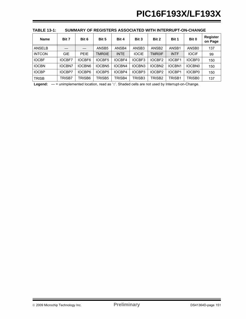
PIC16F193X/LF193X
TABLE 13-1: SUMMARY OF REGISTERS ASSOCIATED WITH INTERRUPT-ON-CHANGE
Name Bit 7 Bit 6 Bit 5 Bit 4 Bit 3 Bit 2 Bit 1 Bit 0Register on Page
ANSELB — — ANSB5 ANSB4 ANSB3 ANSB2 ANSB1 ANSB0 137
INTCON GIE PEIE TMR0IE INTE IOCIE TMR0IF INTF IOCIF 99
IOCBF IOCBF7 IOCBF6 IOCBF5 IOCBF4 IOCBF3 IOCBF2 IOCBF1 IOCBF0 150
IOCBN IOCBN7 IOCBN6 IOCBN5 IOCBN4 IOCBN3 IOCBN2 IOCBN1 IOCBN0 150
IOCBP IOCBP7 IOCBP6 IOCBP5 IOCBP4 IOCBP3 IOCBP2 IOCBP1 IOCBP0 150
TRISB TRISB7 TRISB6 TRISB5 TRISB4 TRISB3 TRISB2 TRISB1 TRISB0 137
Legend: — = unimplemented location, read as ‘0’. Shaded cells are not used by Interrupt-on-Change.
2009 Microchip Technology Inc. Preliminary DS41364D-page 151

PIC16F193X/LF193X
NOTES:
DS41364D-page 152 Preliminary 2009 Microchip Technology Inc.
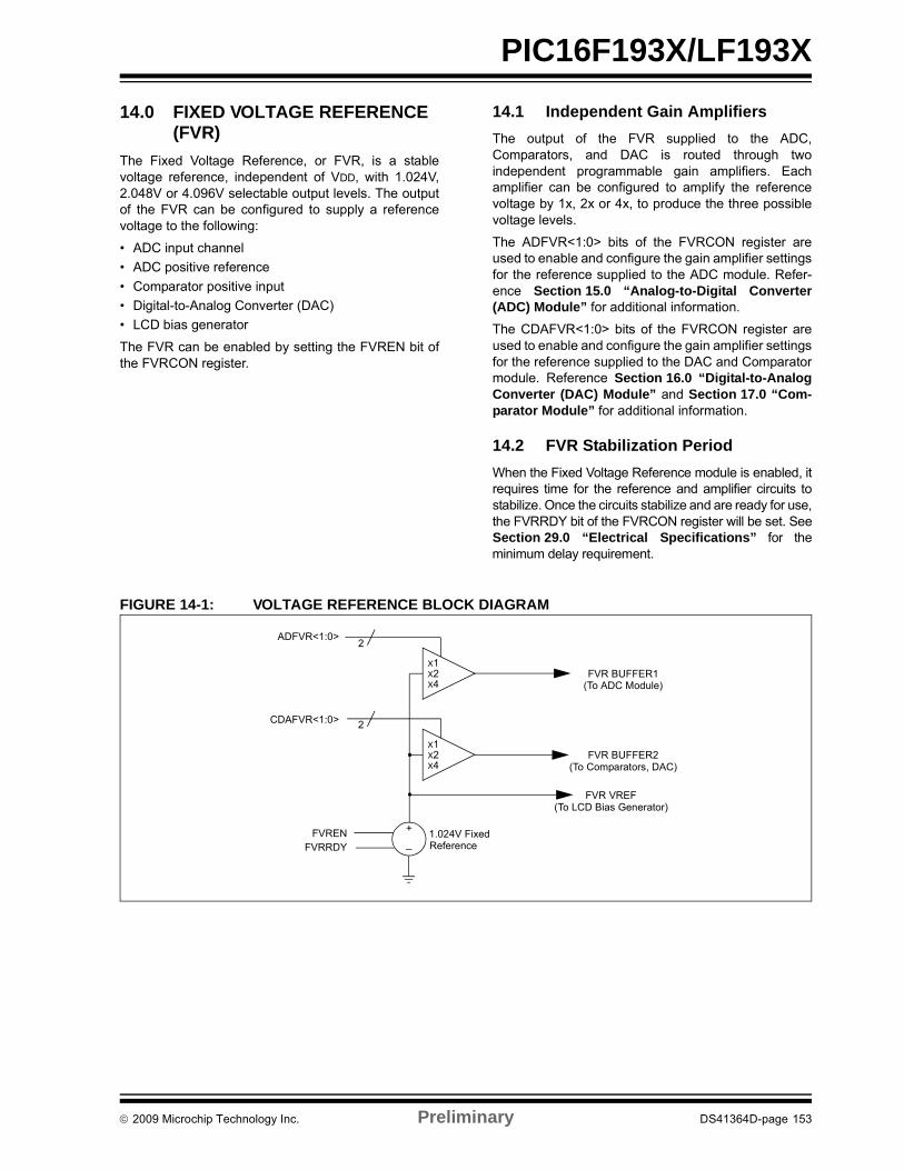
PIC16F193X/LF193X
14.0 FIXED VOLTAGE REFERENCE (FVR)
The Fixed Voltage Reference, or FVR, is a stablevoltage reference, independent of VDD, with 1.024V,2.048V or 4.096V selectable output levels. The outputof the FVR can be configured to supply a referencevoltage to the following:
• ADC input channel
• ADC positive reference
• Comparator positive input
• Digital-to-Analog Converter (DAC)
• LCD bias generator
The FVR can be enabled by setting the FVREN bit ofthe FVRCON register.
14.1 Independent Gain Amplifiers
The output of the FVR supplied to the ADC,Comparators, and DAC is routed through twoindependent programmable gain amplifiers. Eachamplifier can be configured to amplify the referencevoltage by 1x, 2x or 4x, to produce the three possiblevoltage levels.
The ADFVR<1:0> bits of the FVRCON register areused to enable and configure the gain amplifier settingsfor the reference supplied to the ADC module. Refer-ence Section 15.0 “Analog-to-Digital Converter(ADC) Module” for additional information.
The CDAFVR<1:0> bits of the FVRCON register areused to enable and configure the gain amplifier settingsfor the reference supplied to the DAC and Comparatormodule. Reference Section 16.0 “Digital-to-AnalogConverter (DAC) Module” and Section 17.0 “Com-parator Module” for additional information.
14.2 FVR Stabilization Period
When the Fixed Voltage Reference module is enabled, itrequires time for the reference and amplifier circuits tostabilize. Once the circuits stabilize and are ready for use,the FVRRDY bit of the FVRCON register will be set. SeeSection 29.0 “Electrical Specifications” for theminimum delay requirement.
FIGURE 14-1: VOLTAGE REFERENCE BLOCK DIAGRAM
ADFVR<1:0>
CDAFVR<1:0>
X1X2X4
X1X2X4
2
2
FVR BUFFER1(To ADC Module)
FVR BUFFER2(To Comparators, DAC)
FVR VREF(To LCD Bias Generator)
+
_FVREN
FVRRDY1.024V FixedReference
2009 Microchip Technology Inc. Preliminary DS41364D-page 153
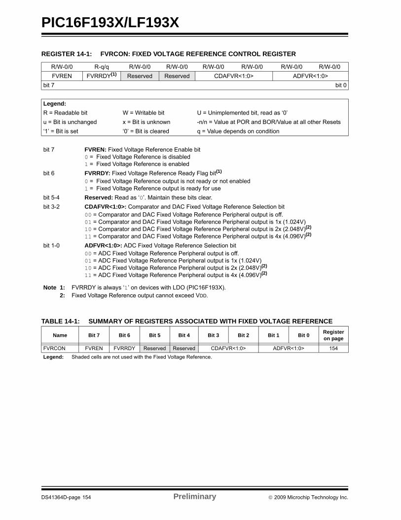
PIC16F193X/LF193X
TABLE 14-1: SUMMARY OF REGISTERS ASSOCIATED WITH FIXED VOLTAGE REFERENCE
REGISTER 14-1: FVRCON: FIXED VOLTAGE REFERENCE CONTROL REGISTER
R/W-0/0 R-q/q R/W-0/0 R/W-0/0 R/W-0/0 R/W-0/0 R/W-0/0 R/W-0/0
FVREN FVRRDY(1) Reserved Reserved CDAFVR<1:0> ADFVR<1:0>
bit 7 bit 0
Legend:
R = Readable bit W = Writable bit U = Unimplemented bit, read as ‘0’
u = Bit is unchanged x = Bit is unknown -n/n = Value at POR and BOR/Value at all other Resets
‘1’ = Bit is set ‘0’ = Bit is cleared q = Value depends on condition
bit 7 FVREN: Fixed Voltage Reference Enable bit0 = Fixed Voltage Reference is disabled1 = Fixed Voltage Reference is enabled
bit 6 FVRRDY: Fixed Voltage Reference Ready Flag bit(1)
0 = Fixed Voltage Reference output is not ready or not enabled1 = Fixed Voltage Reference output is ready for use
bit 5-4 Reserved: Read as ‘0’. Maintain these bits clear.
bit 3-2 CDAFVR<1:0>: Comparator and DAC Fixed Voltage Reference Selection bit00 = Comparator and DAC Fixed Voltage Reference Peripheral output is off.01 = Comparator and DAC Fixed Voltage Reference Peripheral output is 1x (1.024V)10 = Comparator and DAC Fixed Voltage Reference Peripheral output is 2x (2.048V)(2)
11 = Comparator and DAC Fixed Voltage Reference Peripheral output is 4x (4.096V)(2)
bit 1-0 ADFVR<1:0>: ADC Fixed Voltage Reference Selection bit00 = ADC Fixed Voltage Reference Peripheral output is off.01 = ADC Fixed Voltage Reference Peripheral output is 1x (1.024V)10 = ADC Fixed Voltage Reference Peripheral output is 2x (2.048V)(2)
11 = ADC Fixed Voltage Reference Peripheral output is 4x (4.096V)(2)
Note 1: FVRRDY is always ‘1’ on devices with LDO (PIC16F193X).2: Fixed Voltage Reference output cannot exceed VDD.
Name Bit 7 Bit 6 Bit 5 Bit 4 Bit 3 Bit 2 Bit 1 Bit 0Register on page
FVRCON FVREN FVRRDY Reserved Reserved CDAFVR<1:0> ADFVR<1:0> 154
Legend: Shaded cells are not used with the Fixed Voltage Reference.
DS41364D-page 154 Preliminary 2009 Microchip Technology Inc.
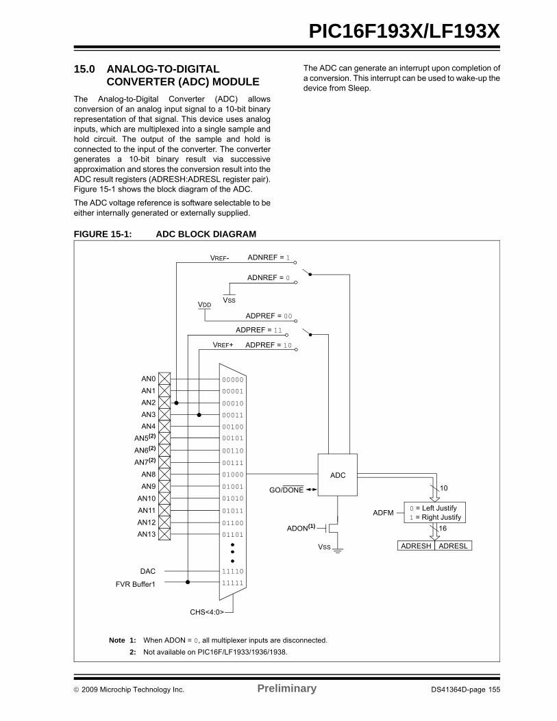
PIC16F193X/LF193X
15.0 ANALOG-TO-DIGITAL CONVERTER (ADC) MODULE
The Analog-to-Digital Converter (ADC) allowsconversion of an analog input signal to a 10-bit binaryrepresentation of that signal. This device uses analoginputs, which are multiplexed into a single sample andhold circuit. The output of the sample and hold isconnected to the input of the converter. The convertergenerates a 10-bit binary result via successiveapproximation and stores the conversion result into theADC result registers (ADRESH:ADRESL register pair).Figure 15-1 shows the block diagram of the ADC.
The ADC voltage reference is software selectable to beeither internally generated or externally supplied.
The ADC can generate an interrupt upon completion ofa conversion. This interrupt can be used to wake-up thedevice from Sleep.
FIGURE 15-1: ADC BLOCK DIAGRAM
DAC
VDD
VREF+ ADPREF = 10
ADPREF = 00
ADPREF = 11
FVR Buffer1
VSS
VREF- ADNREF = 1
ADNREF = 0
Note 1: When ADON = 0, all multiplexer inputs are disconnected.
2: Not available on PIC16F/LF1933/1936/1938.
ADON(1)
GO/DONE
VSS
ADC
00000
00001
00010
00011
00100
00101
00111
00110
01000
01001
01010
01011
01100
01101
11110
CHS<4:0>
AN0
AN1
AN2
AN4
AN5(2)
AN6(2)
AN7(2)
AN3
AN8
AN9
AN10
AN11
AN12
AN13
11111
ADRESH ADRESL
10
16
ADFM0 = Left Justify1 = Right Justify
2009 Microchip Technology Inc. Preliminary DS41364D-page 155
PIC16F193X/LF193X
15.1 ADC Configuration
When configuring and using the ADC the followingfunctions must be considered:
• Port configuration
• Channel selection
• ADC voltage reference selection
• ADC conversion clock source
• Interrupt control
• Result formatting
15.1.1 PORT CONFIGURATION
The ADC can be used to convert both analog anddigital signals. When converting analog signals, the I/Opin should be configured for analog by setting theassociated TRIS and ANSEL bits. Refer to Section “”for more information.
15.1.2 CHANNEL SELECTION
There are 16 channel selections available:
• AN<13:0> pins
• DAC Output
• FVR (Fixed Voltage Reference) Output
Refer to Section 16.0 “Digital-to-Analog Converter(DAC) Module” and Section 14.0 “Fixed VoltageReference (FVR)” for more information on these chan-nel selections.
The CHS bits of the ADCON0 register determine whichchannel is connected to the sample and hold circuit.
When changing channels, a delay is required beforestarting the next conversion. Refer to Section 15.2“ADC Operation” for more information.
15.1.3 ADC VOLTAGE REFERENCE
The ADPREF bits of the ADCON1 register providescontrol of the positive voltage reference. The positivevoltage reference can be:
• VREF+ pin
• VDD
• FVR
The ADNREF bits of the ADCON1 register providescontrol of the negative voltage reference. The negativevoltage reference can be:
• VREF- pin
• VSS
See Section 14.0 “Fixed Voltage Reference (FVR)”for more details on the fixed voltage reference.
15.1.4 CONVERSION CLOCK
The source of the conversion clock is software select-able via the ADCS bits of the ADCON1 register. Thereare seven possible clock options:
• FOSC/2
• FOSC/4
• FOSC/8
• FOSC/16
• FOSC/32
• FOSC/64
• FRC (dedicated internal oscillator)
The time to complete one bit conversion is defined asTAD. One full 10-bit conversion requires 11.5 TAD
periods as shown in Figure 15-2.
For correct conversion, the appropriate TAD specifica-tion must be met. Refer to the A/D conversion require-ments in Section 29.0 “Electrical Specifications” formore information. Table 15-1 gives examples ofappropriate ADC clock selections.
Note: Analog voltages on any pin that is definedas a digital input may cause the input buf-fer to conduct excess current.
Note: Unless using the FRC, any changes in thesystem clock frequency will change theADC clock frequency, which mayadversely affect the ADC result.
DS41364D-page 156 Preliminary 2009 Microchip Technology Inc.

PIC16F193X/LF193X
TABLE 15-1: ADC CLOCK PERIOD (TAD) VS. DEVICE OPERATING FREQUENCIES
FIGURE 15-2: ANALOG-TO-DIGITAL CONVERSION TAD CYCLES
ADC Clock Period (TAD)Device Frequency (FOSC)Device Frequency (FOSC)
ADCClock Source
ADCS<2:0> 32 MHz 20 MHz 16 MHz 8 MHz 4 MHz 1 MHz
Fosc/2 000 62.5ns(2) 100 ns(2) 125 ns(2) 250 ns(2) 500 ns(2) 2.0 s
Fosc/4 100 125 ns(2) 200 ns(2) 250 ns(2) 500 ns(2) 1.0 s 4.0 s
Fosc/8 001 0.5 s(2) 400 ns(2) 0.5 s(2) 1.0 s 2.0 s 8.0 s(3)
Fosc/16 101 800 ns 800 ns 1.0 s 2.0 s 4.0 s 16.0 s(3)
Fosc/32 010 1.0 s 1.6 s 2.0 s 4.0 s 8.0 s(3) 32.0 s(3)
Fosc/64 110 2.0 s 3.2 s 4.0 s 8.0 s(3) 16.0 s(3) 64.0 s(3)
FRC x11 1.0-6.0 s(1,4) 1.0-6.0 s(1,4) 1.0-6.0 s(1,4) 1.0-6.0 s(1,4) 1.0-6.0 s(1,4) 1.0-6.0 s(1,4)
Legend: Shaded cells are outside of recommended range.Note 1: The FRC source has a typical TAD time of 1.6 s for VDD.
2: These values violate the minimum required TAD time.3: For faster conversion times, the selection of another clock source is recommended.4: The ADC clock period (TAD) and total ADC conversion time can be minimized when the ADC clock is derived from the
system clock FOSC. However, the FRC clock source must be used when conversions are to be performed with the device in Sleep mode.
TAD1 TAD2 TAD3 TAD4 TAD5 TAD6 TAD7 TAD8 TAD11
Set GO bit
Holding capacitor is disconnected from analog input (typically 100 ns)
TAD9 TAD10TCY - TAD
ADRESH:ADRESL is loaded, GO bit is cleared, ADIF bit is set, holding capacitor is connected to analog input.
Conversion starts
b0b9 b6 b5 b4 b3 b2 b1b8 b7
On the following cycle:
2009 Microchip Technology Inc. Preliminary DS41364D-page 157
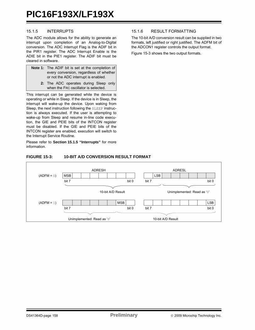
PIC16F193X/LF193X
15.1.5 INTERRUPTS
The ADC module allows for the ability to generate aninterrupt upon completion of an Analog-to-Digitalconversion. The ADC Interrupt Flag is the ADIF bit inthe PIR1 register. The ADC Interrupt Enable is theADIE bit in the PIE1 register. The ADIF bit must becleared in software.
This interrupt can be generated while the device isoperating or while in Sleep. If the device is in Sleep, theinterrupt will wake-up the device. Upon waking fromSleep, the next instruction following the SLEEP instruc-tion is always executed. If the user is attempting towake-up from Sleep and resume in-line code execu-tion, the GIE and PEIE bits of the INTCON registermust be disabled. If the GIE and PEIE bits of theINTCON register are enabled, execution will switch tothe Interrupt Service Routine.
Please refer to Section 15.1.5 “Interrupts” for moreinformation.
15.1.6 RESULT FORMATTING
The 10-bit A/D conversion result can be supplied in twoformats, left justified or right justified. The ADFM bit ofthe ADCON1 register controls the output format.
Figure 15-3 shows the two output formats.
FIGURE 15-3: 10-BIT A/D CONVERSION RESULT FORMAT
Note 1: The ADIF bit is set at the completion ofevery conversion, regardless of whetheror not the ADC interrupt is enabled.
2: The ADC operates during Sleep onlywhen the FRC oscillator is selected.
ADRESH ADRESL
(ADFM = 0) MSB LSB
bit 7 bit 0 bit 7 bit 0
10-bit A/D Result Unimplemented: Read as ‘0’
(ADFM = 1) MSB LSB
bit 7 bit 0 bit 7 bit 0
Unimplemented: Read as ‘0’ 10-bit A/D Result
DS41364D-page 158 Preliminary 2009 Microchip Technology Inc.

PIC16F193X/LF193X
15.2 ADC Operation
15.2.1 STARTING A CONVERSION
To enable the ADC module, the ADON bit of theADCON0 register must be set to a ‘1’. Setting the GO/DONE bit of the ADCON0 register to a ‘1’ will start theAnalog-to-Digital conversion.
15.2.2 COMPLETION OF A CONVERSION
When the conversion is complete, the ADC module will:
• Clear the GO/DONE bit
• Set the ADIF Interrupt Flag bit
• Update the ADRESH and ADRESL registers with new conversion result
15.2.3 TERMINATING A CONVERSION
If a conversion must be terminated before completion,the GO/DONE bit can be cleared in software. TheADRESH and ADRESL registers will be updated withthe partially complete Analog-to-Digital conversionsample. Incomplete bits will match the last bitconverted.
15.2.4 ADC OPERATION DURING SLEEP
The ADC module can operate during Sleep. Thisrequires the ADC clock source to be set to the FRC
option. When the FRC clock source is selected, theADC waits one additional instruction before starting theconversion. This allows the SLEEP instruction to beexecuted, which can reduce system noise during theconversion. If the ADC interrupt is enabled, the devicewill wake-up from Sleep when the conversioncompletes. If the ADC interrupt is disabled, the ADCmodule is turned off after the conversion completes,although the ADON bit remains set.
When the ADC clock source is something other thanFRC, a SLEEP instruction causes the present conver-sion to be aborted and the ADC module is turned off,although the ADON bit remains set.
15.2.5 SPECIAL EVENT TRIGGER
The Special Event Trigger of the CCPx/ECCPX moduleallows periodic ADC measurements without softwareintervention. When this trigger occurs, the GO/DONEbit is set by hardware and the Timer1 counter resets tozero.
Using the Special Event Trigger does not assure properADC timing. It is the user’s responsibility to ensure thatthe ADC timing requirements are met.
Refer to Section 22.0 “Capture/Compare/PWMModules” for more information.
Note: The GO/DONE bit should not be set in thesame instruction that turns on the ADC.Refer to Section 15.2.6 “A/D Conver-sion Procedure”.
Note: A device Reset forces all registers to theirReset state. Thus, the ADC module isturned off and any pending conversion isterminated.
TABLE 15-2: SPECIAL EVENT TRIGGER
Device CCPx/ECCPx
PIC16F193X/LF193X CCP5
2009 Microchip Technology Inc. Preliminary DS41364D-page 159

PIC16F193X/LF193X
15.2.6 A/D CONVERSION PROCEDURE
This is an example procedure for using the ADC toperform an Analog-to-Digital conversion:
1. Configure Port:
• Disable pin output driver (Refer to the TRIS register)
• Configure pin as analog (Refer to the ANSEL register)
2. Configure the ADC module:
• Select ADC conversion clock
• Configure voltage reference
• Select ADC input channel
• Turn on ADC module
3. Configure ADC interrupt (optional):
• Clear ADC interrupt flag
• Enable ADC interrupt
• Enable peripheral interrupt
• Enable global interrupt(1)
4. Wait the required acquisition time(2).
5. Start conversion by setting the GO/DONE bit.
6. Wait for ADC conversion to complete by one ofthe following:
• Polling the GO/DONE bit
• Waiting for the ADC interrupt (interrupts enabled)
7. Read ADC Result.
8. Clear the ADC interrupt flag (required if interruptis enabled).
EXAMPLE 15-1: A/D CONVERSION
Note 1: The global interrupt can be disabled if theuser is attempting to wake-up from Sleepand resume in-line code execution.
2: Refer to Section 15.3 “A/D AcquisitionRequirements”.
;This code block configures the ADC;for polling, Vdd and Vss references, Frc ;clock and AN0 input.;;Conversion start & polling for completion ; are included.;BANKSEL ADCON1 ;MOVLW B’11110000’ ;Right justify, Frc
;clockMOVWF ADCON1 ;Vdd and Vss VrefBANKSEL TRISA ;BSF TRISA,0 ;Set RA0 to inputBANKSEL ANSEL ;BSF ANSEL,0 ;Set RA0 to analogBANKSEL ADCON0 ;MOVLW B’00000001’ ;Select channel AN0MOVWF ADCON0 ;Turn ADC OnCALL SampleTime ;Acquisiton delayBSF ADCON0,ADGO ;Start conversionBTFSC ADCON0,ADGO ;Is conversion done?GOTO $-1 ;No, test againBANKSEL ADRESH ;MOVF ADRESH,W ;Read upper 2 bitsMOVWF RESULTHI ;store in GPR spaceBANKSEL ADRESL ;MOVF ADRESL,W ;Read lower 8 bitsMOVWF RESULTLO ;Store in GPR space
DS41364D-page 160 Preliminary 2009 Microchip Technology Inc.
PIC16F193X/LF193X
15.2.7 ADC REGISTER DEFINITIONS
The following registers are used to control theoperation of the ADC.
REGISTER 15-1: ADCON0: A/D CONTROL REGISTER 0
U-0 R/W-0/0 R/W-0/0 R/W-0/0 R/W-0/0 R/W-0/0 R/W-0/0 R/W-0/0
— CHS<4:0> GO/DONE ADON
bit 7 bit 0
Legend:
R = Readable bit W = Writable bit U = Unimplemented bit, read as ‘0’
u = Bit is unchanged x = Bit is unknown -n/n = Value at POR and BOR/Value at all other Resets
‘1’ = Bit is set ‘0’ = Bit is cleared
bit 7 Unimplemented: Read as ‘0’
bit 6-2 CHS<4:0>: Analog Channel Select bits
00000 = AN000001 = AN100010 = AN200011 = AN300100 = AN400101 = AN5(3)
00110 = AN6(3)
00111 = AN7(3)
01000 = AN801001 = AN901010 = AN1001011 = AN1101100 = AN1201101 = AN1301110 = Reserved. No channel connected.
• • •
11101 = Reserved. No channel connected.11110 = DAC output(1)
11111 = FVR (Fixed Voltage Reference) Buffer 1 Output(2)
bit 1 GO/DONE: A/D Conversion Status bit
1 = A/D conversion cycle in progress. Setting this bit starts an A/D conversion cycle. This bit is automatically cleared by hardware when the A/D conversion has completed.0 = A/D conversion completed/not in progress
bit 0 ADON: ADC Enable bit1 = ADC is enabled0 = ADC is disabled and consumes no operating current
Note 1: See Section 16.0 “Digital-to-Analog Converter (DAC) Module” for more information.
2: See Section 14.0 “Fixed Voltage Reference (FVR)” for more information.
3: Not available on the PIC16F/LF1933/1936/1938.
2009 Microchip Technology Inc. Preliminary DS41364D-page 161
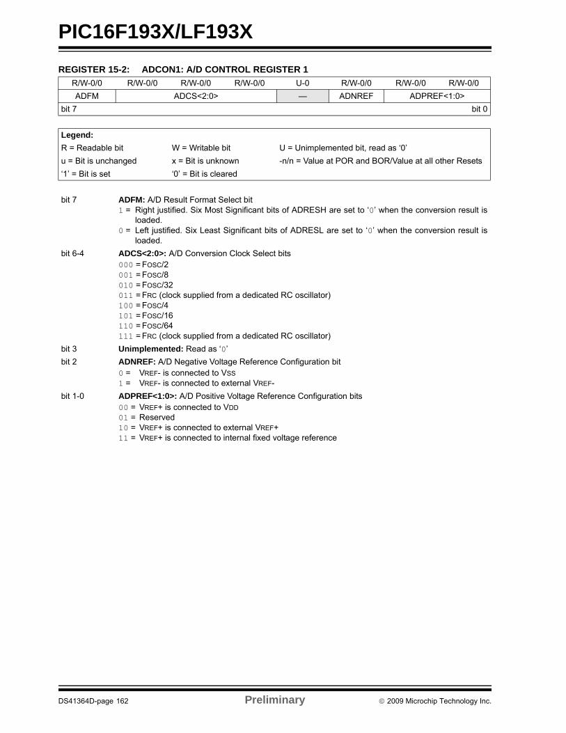
PIC16F193X/LF193X
REGISTER 15-2: ADCON1: A/D CONTROL REGISTER 1
R/W-0/0 R/W-0/0 R/W-0/0 R/W-0/0 U-0 R/W-0/0 R/W-0/0 R/W-0/0
ADFM ADCS<2:0> — ADNREF ADPREF<1:0>
bit 7 bit 0
Legend:
R = Readable bit W = Writable bit U = Unimplemented bit, read as ‘0’
u = Bit is unchanged x = Bit is unknown -n/n = Value at POR and BOR/Value at all other Resets
‘1’ = Bit is set ‘0’ = Bit is cleared
bit 7 ADFM: A/D Result Format Select bit1 = Right justified. Six Most Significant bits of ADRESH are set to ‘0’ when the conversion result is
loaded.0 = Left justified. Six Least Significant bits of ADRESL are set to ‘0’ when the conversion result is
loaded.
bit 6-4 ADCS<2:0>: A/D Conversion Clock Select bits000 = FOSC/2001 = FOSC/8010 = FOSC/32011 = FRC (clock supplied from a dedicated RC oscillator)100 = FOSC/4101 = FOSC/16110 = FOSC/64111 = FRC (clock supplied from a dedicated RC oscillator)
bit 3 Unimplemented: Read as ‘0’
bit 2 ADNREF: A/D Negative Voltage Reference Configuration bit0 = VREF- is connected to VSS
1 = VREF- is connected to external VREF-
bit 1-0 ADPREF<1:0>: A/D Positive Voltage Reference Configuration bits00 = VREF+ is connected to VDD
01 = Reserved10 = VREF+ is connected to external VREF+11 = VREF+ is connected to internal fixed voltage reference
DS41364D-page 162 Preliminary 2009 Microchip Technology Inc.
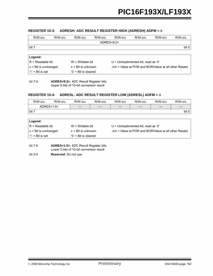
PIC16F193X/LF193X
REGISTER 15-3: ADRESH: ADC RESULT REGISTER HIGH (ADRESH) ADFM = 0
R/W-x/u R/W-x/u R/W-x/u R/W-x/u R/W-x/u R/W-x/u R/W-x/u R/W-x/u
ADRES<9:2>
bit 7 bit 0
Legend:
R = Readable bit W = Writable bit U = Unimplemented bit, read as ‘0’
u = Bit is unchanged x = Bit is unknown -n/n = Value at POR and BOR/Value at all other Resets
‘1’ = Bit is set ‘0’ = Bit is cleared
bit 7-0 ADRES<9:2>: ADC Result Register bitsUpper 8 bits of 10-bit conversion result
REGISTER 15-4: ADRESL: ADC RESULT REGISTER LOW (ADRESL) ADFM = 0
R/W-x/u R/W-x/u R/W-x/u R/W-x/u R/W-x/u R/W-x/u R/W-x/u R/W-x/u
ADRES<1:0> — — — — — —
bit 7 bit 0
Legend:
R = Readable bit W = Writable bit U = Unimplemented bit, read as ‘0’
u = Bit is unchanged x = Bit is unknown -n/n = Value at POR and BOR/Value at all other Resets
‘1’ = Bit is set ‘0’ = Bit is cleared
bit 7-6 ADRES<1:0>: ADC Result Register bitsLower 2 bits of 10-bit conversion result
bit 5-0 Reserved: Do not use.
2009 Microchip Technology Inc. Preliminary DS41364D-page 163
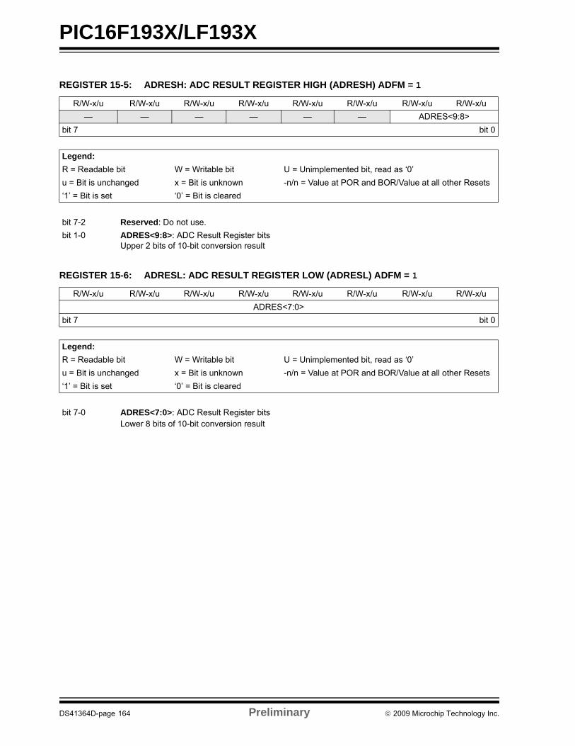
PIC16F193X/LF193X
REGISTER 15-5: ADRESH: ADC RESULT REGISTER HIGH (ADRESH) ADFM = 1
R/W-x/u R/W-x/u R/W-x/u R/W-x/u R/W-x/u R/W-x/u R/W-x/u R/W-x/u
— — — — — — ADRES<9:8>
bit 7 bit 0
Legend:
R = Readable bit W = Writable bit U = Unimplemented bit, read as ‘0’
u = Bit is unchanged x = Bit is unknown -n/n = Value at POR and BOR/Value at all other Resets
‘1’ = Bit is set ‘0’ = Bit is cleared
bit 7-2 Reserved: Do not use.
bit 1-0 ADRES<9:8>: ADC Result Register bitsUpper 2 bits of 10-bit conversion result
REGISTER 15-6: ADRESL: ADC RESULT REGISTER LOW (ADRESL) ADFM = 1
R/W-x/u R/W-x/u R/W-x/u R/W-x/u R/W-x/u R/W-x/u R/W-x/u R/W-x/u
ADRES<7:0>
bit 7 bit 0
Legend:
R = Readable bit W = Writable bit U = Unimplemented bit, read as ‘0’
u = Bit is unchanged x = Bit is unknown -n/n = Value at POR and BOR/Value at all other Resets
‘1’ = Bit is set ‘0’ = Bit is cleared
bit 7-0 ADRES<7:0>: ADC Result Register bitsLower 8 bits of 10-bit conversion result
DS41364D-page 164 Preliminary 2009 Microchip Technology Inc.

PIC16F193X/LF193X
15.3 A/D Acquisition Requirements
For the ADC to meet its specified accuracy, the chargeholding capacitor (CHOLD) must be allowed to fullycharge to the input channel voltage level. The AnalogInput model is shown in Figure 15-4. The sourceimpedance (RS) and the internal sampling switch (RSS)impedance directly affect the time required to chargethe capacitor CHOLD. The sampling switch (RSS)impedance varies over the device voltage (VDD), referto Figure 15-4. The maximum recommendedimpedance for analog sources is 10 k. As the
source impedance is decreased, the acquisition timemay be decreased. After the analog input channel isselected (or changed), an A/D acquisition must bedone before the conversion can be started. To calculatethe minimum acquisition time, Equation 15-1 may beused. This equation assumes that 1/2 LSb error is used(1,024 steps for the ADC). The 1/2 LSb error is themaximum error allowed for the ADC to meet itsspecified resolution.
EQUATION 15-1: ACQUISITION TIME EXAMPLE
TACQ Amplifier Settling Time Hold Capacitor Charging Time Temperature Coefficient+ +=
TAMP TC TCOFF+ +=
2µs TC Temperature - 25°C 0.05µs/°C + +=
TC CHOLD RIC RSS RS+ + ln(1/511)–=
10pF 1k 7k 10k+ + – ln(0.001957)=
1.12= µs
VAPPLIED 1 e
Tc–RC---------
–
VAPPLIED 11
2n 1+ 1–
--------------------------– =
VAPPLIED 11
2n 1+ 1–
--------------------------– VCHOLD=
VAPPLIED 1 e
TC–RC----------
–
VCHOLD=
;[1] VCHOLD charged to within 1/2 lsb
;[2] VCHOLD charge response to VAPPLIED
;combining [1] and [2]
The value for TC can be approximated with the following equations:
Solving for TC:
Therefore:
Temperature 50°C and external impedance of 10k 5.0V VDD=Assumptions:
Note: Where n = number of bits of the ADC.
TACQ 2µs 1.12µs 50°C- 25°C 0.05ΜS/°C + +=
4.42µs=
Note 1: The reference voltage (VREF) has no effect on the equation, since it cancels itself out.
2: The charge holding capacitor (CHOLD) is not discharged after each conversion.
3: The maximum recommended impedance for analog sources is 10 k. This is required to meet the pin leakage specification.
2009 Microchip Technology Inc. Preliminary DS41364D-page 165
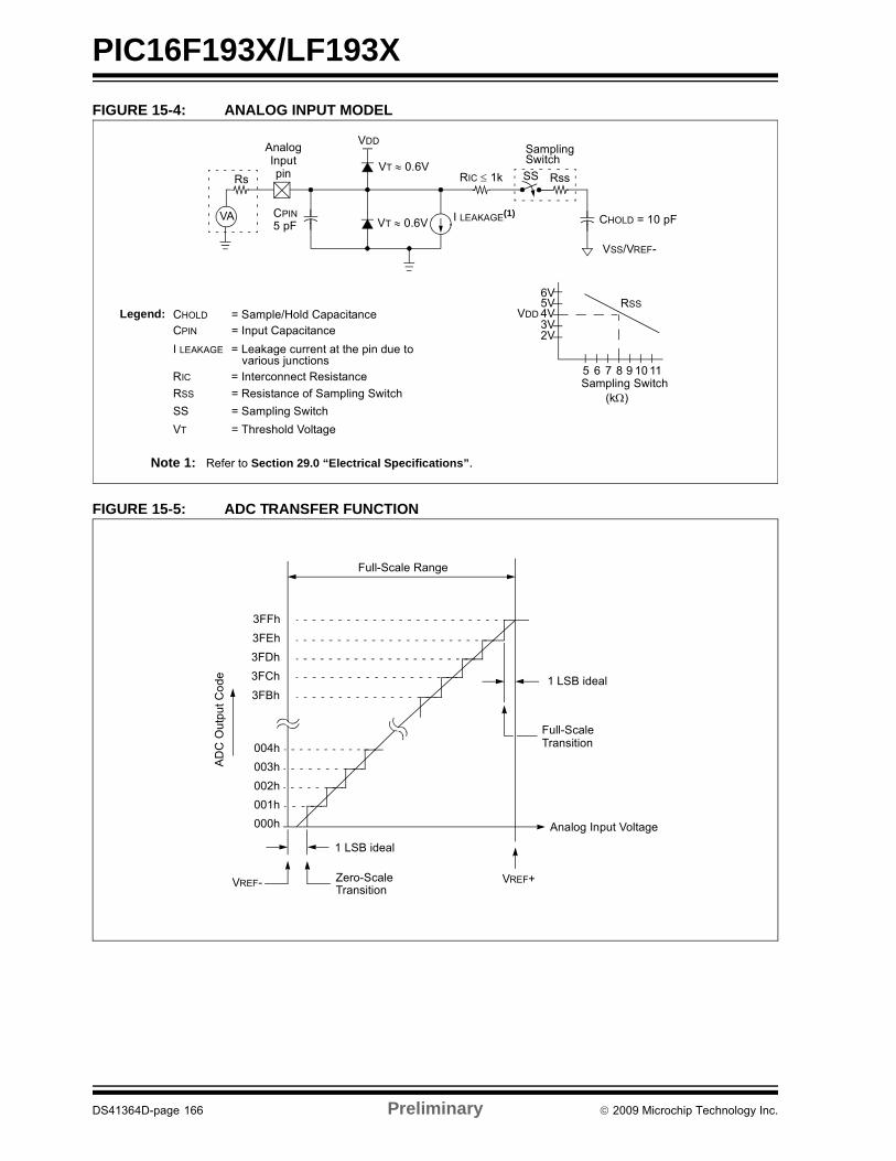
PIC16F193X/LF193X
FIGURE 15-4: ANALOG INPUT MODEL
FIGURE 15-5: ADC TRANSFER FUNCTION
CPINVA
Rs
Analog
5 pF
VDD
VT 0.6V
VT 0.6V I LEAKAGE(1)
RIC 1k
SamplingSwitch
SS Rss
CHOLD = 10 pF
VSS/VREF-
6V
Sampling Switch
5V4V3V2V
5 6 7 8 9 10 11
(k)
VDD
Legend:
CPIN
VT
I LEAKAGE
RIC
SS
CHOLD
= Input Capacitance
= Threshold Voltage
= Leakage current at the pin due to
= Interconnect Resistance
= Sampling Switch
= Sample/Hold Capacitance
various junctions
RSS
Note 1: Refer to Section 29.0 “Electrical Specifications”.
RSS = Resistance of Sampling Switch
Inputpin
3FFh
3FEh
AD
C O
utp
ut C
od
e
3FDh
3FCh
004h
003h
002h
001h
000h
Full-Scale
3FBh
1 LSB ideal
VREF- Zero-ScaleTransition
VREF+
Transition
1 LSB ideal
Full-Scale Range
Analog Input Voltage
DS41364D-page 166 Preliminary 2009 Microchip Technology Inc.
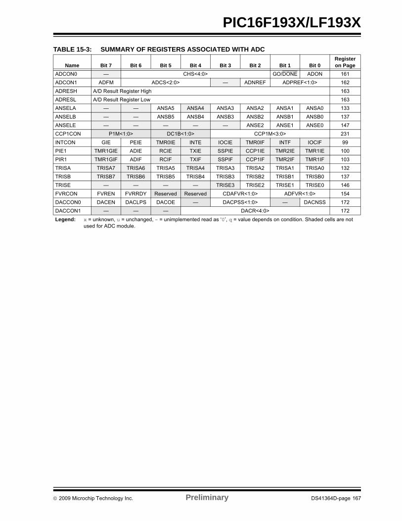
PIC16F193X/LF193X
TABLE 15-3: SUMMARY OF REGISTERS ASSOCIATED WITH ADC
Name Bit 7 Bit 6 Bit 5 Bit 4 Bit 3 Bit 2 Bit 1 Bit 0Register on Page
ADCON0 — CHS<4:0> GO/DONE ADON 161
ADCON1 ADFM ADCS<2:0> — ADNREF ADPREF<1:0> 162
ADRESH A/D Result Register High 163
ADRESL A/D Result Register Low 163
ANSELA — — ANSA5 ANSA4 ANSA3 ANSA2 ANSA1 ANSA0 133
ANSELB — — ANSB5 ANSB4 ANSB3 ANSB2 ANSB1 ANSB0 137
ANSELE — — — — — ANSE2 ANSE1 ANSE0 147
CCP1CON P1M<1:0> DC1B<1:0> CCP1M<3:0> 231
INTCON GIE PEIE TMR0IE INTE IOCIE TMR0IF INTF IOCIF 99
PIE1 TMR1GIE ADIE RCIE TXIE SSPIE CCP1IE TMR2IE TMR1IE 100
PIR1 TMR1GIF ADIF RCIF TXIF SSPIF CCP1IF TMR2IF TMR1IF 103
TRISA TRISA7 TRISA6 TRISA5 TRISA4 TRISA3 TRISA2 TRISA1 TRISA0 132
TRISB TRISB7 TRISB6 TRISB5 TRISB4 TRISB3 TRISB2 TRISB1 TRISB0 137
TRISE — — — — TRISE3 TRISE2 TRISE1 TRISE0 146
FVRCON FVREN FVRRDY Reserved Reserved CDAFVR<1:0> ADFVR<1:0> 154
DACCON0 DACEN DACLPS DACOE — DACPSS<1:0> — DACNSS 172
DACCON1 — — — DACR<4:0> 172
Legend: x = unknown, u = unchanged, — = unimplemented read as ‘0’, q = value depends on condition. Shaded cells are not used for ADC module.
2009 Microchip Technology Inc. Preliminary DS41364D-page 167

PIC16F193X/LF193X
NOTES:
DS41364D-page 168 Preliminary 2009 Microchip Technology Inc.
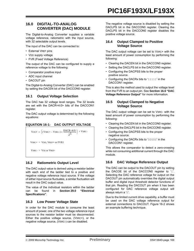
PIC16F193X/LF193X
16.0 DIGITAL-TO-ANALOG CONVERTER (DAC) MODULE
The Digital-to-Analog Converter supplies a variablevoltage reference, ratiometric with the input source,with 32 selectable output levels.
The input of the DAC can be connected to:
• External VREF pins
• VDD supply voltage
• FVR (Fixed Voltage Reference)
The output of the DAC can be configured to supply areference voltage to the following:
• Comparator positive input
• ADC input channel
• DACOUT pin
The Digital-to-Analog Converter (DAC) can be enabledby setting the DACEN bit of the DACCON0 register.
16.1 Output Voltage Selection
The DAC has 32 voltage level ranges. The 32 levelsare set with the DACR<4:0> bits of the DACCON1register.
The DAC output voltage is determined by the followingequations:
EQUATION 16-1: DAC OUTPUT VOLTAGE
16.2 Ratiometric Output Level
The DAC output value is derived using a resistor ladderwith each end of the ladder tied to a positive andnegative voltage reference input source. If the voltageof either input source fluctuates, a similar fluctuation willresult in the DAC output value.
The value of the individual resistors within the laddercan be found in Section 29.0 “ElectricalSpecifications”.
16.3 Low Power Voltage State
In order for the DAC module to consume the leastamount of power, one of the two voltage reference inputsources to the resistor ladder must be disconnected.Either the positive voltage source, (VSRC+), or thenegative voltage source, (VSRC-) can be disabled.
The negative voltage source is disabled by setting theDACLPS bit in the DACCON0 register. Clearing theDACLPS bit in the DACCON0 register disables thepositive voltage source.
16.4 Output Clamped to Positive Voltage Source
The DAC output voltage can be set to VSRC+ with theleast amount of power consumption by performing thefollowing:
• Clearing the DACEN bit in the DACCON0 register.
• Setting the DACLPS bit in the DACCON0 register.
• Configuring the DACPSS bits to the proper positive source.
• Configuring the DACRx bits to ‘11111’ in the DACCON1 register.
This is also the method used to output the voltage levelfrom the FVR to an output pin. See Section 16.6 “DACVoltage Reference Output” for more information.
16.5 Output Clamped to Negative Voltage Source
The DAC output voltage can be set to VSRC- with theleast amount of power consumption by performing thefollowing:
• Clearing the DACEN bit in the DACCON0 register.
• Clearing the DACLPS bit in the DACCON0 register.
• Configuring the DACPSS bits to the proper negative source.
• Configuring the DACRx bits to ‘00000’ in the DACCON1 register.
This allows the comparator to detect a zero-crossingwhile not consuming additional current through the DACmodule.
16.6 DAC Voltage Reference Output
The DAC can be output to the DACOUT pin by settingthe DACOE bit of the DACCON0 register to ‘1’.Selecting the DAC reference voltage for output on theDACOUT pin automatically overrides the digital outputbuffer and digital input threshold detector functions ofthat pin. Reading the DACOUT pin when it has beenconfigured for DAC reference voltage output willalways return a ‘0’.
Due to the limited current drive capability, a buffer mustbe used on the DAC voltage reference output forexternal connections to DACOUT. Figure 16-2 showsan example buffering technique.
VOUT VSRC+ VSRC-– DACR<4:0>
25-------------------------------
= + VSRC-
VSRC+ = VDD, VREF+ or FVR1
VSRC- = VSS or VREF-
2009 Microchip Technology Inc. Preliminary DS41364D-page 169
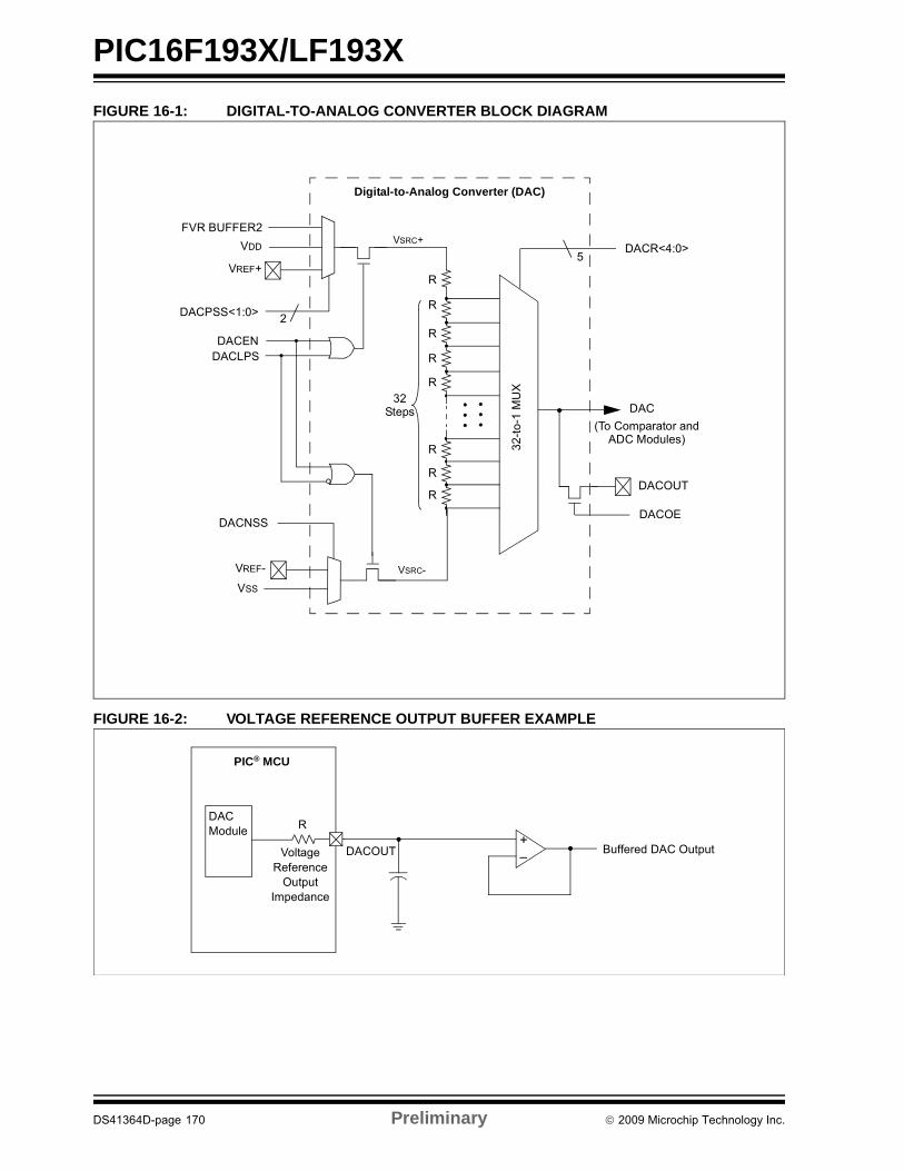
PIC16F193X/LF193X
FIGURE 16-1: DIGITAL-TO-ANALOG CONVERTER BLOCK DIAGRAM
FIGURE 16-2: VOLTAGE REFERENCE OUTPUT BUFFER EXAMPLE
32
-to
-1 M
UX
DACR<4:0>
R
VREF-
DACNSS
R
R
R
R
R
R
32DAC
DACOUT
5
(To Comparator andADC Modules)
DACOE
VDD
VREF+
DACPSS<1:0> 2
DACEN
Steps
Digital-to-Analog Converter (DAC)
FVR BUFFER2
R
VSRC-
VSRC+
VSS
DACLPS
DACOUT Buffered DAC Output+–
DACModule
Voltage Reference
Output Impedance
R
PIC® MCU
DS41364D-page 170 Preliminary 2009 Microchip Technology Inc.

PIC16F193X/LF193X
16.7 Operation During Sleep
When the device wakes up from Sleep through aninterrupt or a Watchdog Timer time-out, the contents ofthe DACCON0 register are not affected. To minimizecurrent consumption in Sleep mode, the voltagereference should be disabled.
16.8 Effects of a Reset
A device Reset affects the following:
• DAC is disabled.
• DAC output voltage is removed from the DACOUT pin.
• The DACR<4:0> range select bits are cleared.
2009 Microchip Technology Inc. Preliminary DS41364D-page 171

PIC16F193X/LF193X
REGISTER 16-1: DACCON0: VOLTAGE REFERENCE CONTROL REGISTER 0
R/W-0/0 R/W-0/0 R/W-0/0 U-0 R/W-0/0 R/W-0/0 U-0 R/W-0/0
DACEN DACLPS DACOE --- DACPSS<1:0> --- DACNSS
bit 7 bit 0
Legend:
R = Readable bit W = Writable bit U = Unimplemented bit, read as ‘0’
u = Bit is unchanged x = Bit is unknown -n/n = Value at POR and BOR/Value at all other Resets
‘1’ = Bit is set ‘0’ = Bit is cleared
bit 7 DACEN: DAC Enable bit1 = DAC is enabled0 = DAC is disabled
bit 6 DACLPS: DAC Low-Power Voltage State Select bit
1 = DAC Positive reference source selected0 = DAC Negative reference source selected
bit 5 DACOE: DAC Voltage Output Enable bit1 = DAC voltage level is also an output on the DACOUT pin0 = DAC voltage level is disconnected from the DACOUT pin
bit 4 Unimplemented: Read as ‘0’
bit 3-2 DACPSS<1:0>: DAC Positive Source Select bits00 = VDD
01 = VREF+10 = FVR Buffer2 output11 = Reserved, do not use
bit 1 Unimplemented: Read as ‘0’
bit 0 DACNSS: DAC Negative Source Select bits1 = VREF-0 = VSS
REGISTER 16-2: DACCON1: VOLTAGE REFERENCE CONTROL REGISTER 1
U-0 U-0 U-0 R/W-0/0 R/W-0/0 R/W-0/0 R/W-0/0 R/W-0/0
--- --- --- DACR<4:0>
bit 7 bit 0
Legend:
R = Readable bit W = Writable bit U = Unimplemented bit, read as ‘0’
u = Bit is unchanged x = Bit is unknown -n/n = Value at POR and BOR/Value at all other Resets
‘1’ = Bit is set ‘0’ = Bit is cleared
bit 7-5 Unimplemented: Read as ‘0’
bit 4-0 DACR<4:0>: DAC Voltage Output Select bits
VOUT = ((VSRC+) - (VSRC-))*(DACR<4:0>/(25)) + VSRC-
Note 1: The output select bits are always right justified to ensure that any number of bits can be used without affecting the register layout.
DS41364D-page 172 Preliminary 2009 Microchip Technology Inc.
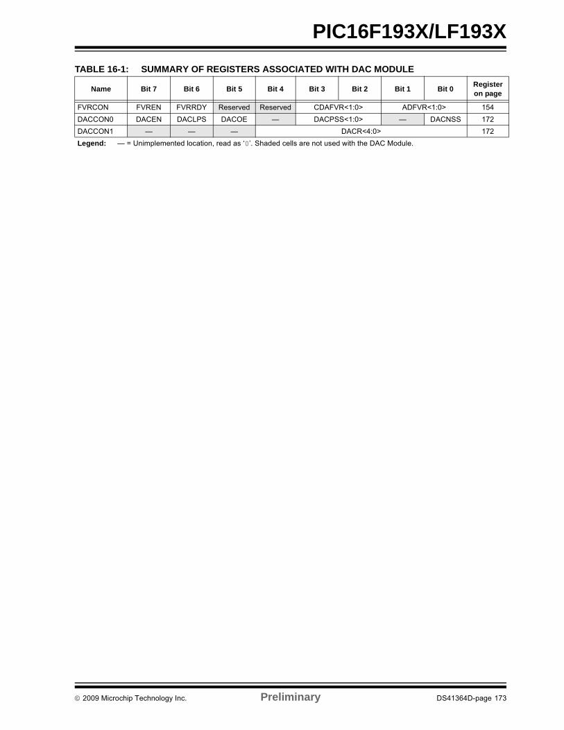
PIC16F193X/LF193X
TABLE 16-1: SUMMARY OF REGISTERS ASSOCIATED WITH DAC MODULE
Name Bit 7 Bit 6 Bit 5 Bit 4 Bit 3 Bit 2 Bit 1 Bit 0Register on page
FVRCON FVREN FVRRDY Reserved Reserved CDAFVR<1:0> ADFVR<1:0> 154
DACCON0 DACEN DACLPS DACOE — DACPSS<1:0> — DACNSS 172
DACCON1 — — — DACR<4:0> 172
Legend: — = Unimplemented location, read as ‘0’. Shaded cells are not used with the DAC Module.
2009 Microchip Technology Inc. Preliminary DS41364D-page 173

PIC16F193X/LF193X
NOTES:
DS41364D-page 174 Preliminary 2009 Microchip Technology Inc.
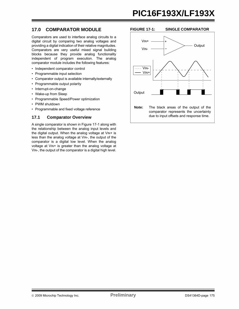
PIC16F193X/LF193X
17.0 COMPARATOR MODULE
Comparators are used to interface analog circuits to adigital circuit by comparing two analog voltages andproviding a digital indication of their relative magnitudes.Comparators are very useful mixed signal buildingblocks because they provide analog functionalityindependent of program execution. The analogcomparator module includes the following features:
• Independent comparator control
• Programmable input selection
• Comparator output is available internally/externally
• Programmable output polarity
• Interrupt-on-change
• Wake-up from Sleep
• Programmable Speed/Power optimization
• PWM shutdown
• Programmable and fixed voltage reference
17.1 Comparator Overview
A single comparator is shown in Figure 17-1 along withthe relationship between the analog input levels andthe digital output. When the analog voltage at VIN+ isless than the analog voltage at VIN-, the output of thecomparator is a digital low level. When the analogvoltage at VIN+ is greater than the analog voltage atVIN-, the output of the comparator is a digital high level.
FIGURE 17-1: SINGLE COMPARATOR
–
+VIN+
VIN-Output
Output
VIN+VIN-
Note: The black areas of the output of thecomparator represents the uncertaintydue to input offsets and response time.
2009 Microchip Technology Inc. Preliminary DS41364D-page 175
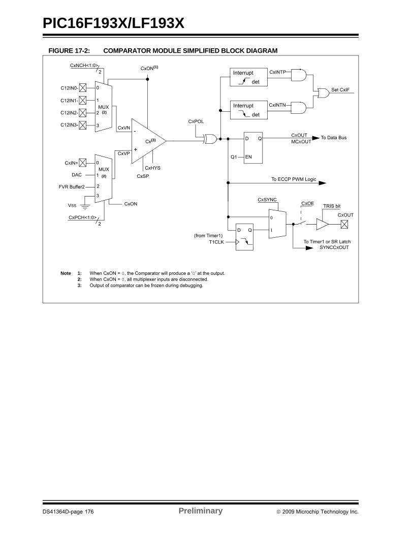
PIC16F193X/LF193X
FIGURE 17-2: COMPARATOR MODULE SIMPLIFIED BLOCK DIAGRAM
Note 1: When CxON = 0, the Comparator will produce a ‘0’ at the output.2: When CxON = 0, all multiplexer inputs are disconnected.3: Output of comparator can be frozen during debugging.
MUX
Cx(3)
0
1
2
3
CxON(1)CxNCH<1:0>2
0
1
CXPCH<1:0>
C12IN1-
C12IN2-
C12IN3-
CXIN+MUX
-
+
CxVN
CxVP
CXOUT
To ECCP PWM Logic
Q1
D
EN
Q
CXPOL
MCXOUT
Set CxIF
0
1
CXSYNCCXOE
CXOUT
D Q
SYNCCXOUT
DAC
FVR Buffer2
C12IN0-
2
CxSP
CxHYS
det
Interrupt
det
Interrupt
To Timer1 or SR Latch
CxINTN
CxINTP
To Data Bus
2
3
VSS TRIS bitCxON
(2)
(2)
(from Timer1)T1CLK
DS41364D-page 176 Preliminary 2009 Microchip Technology Inc.
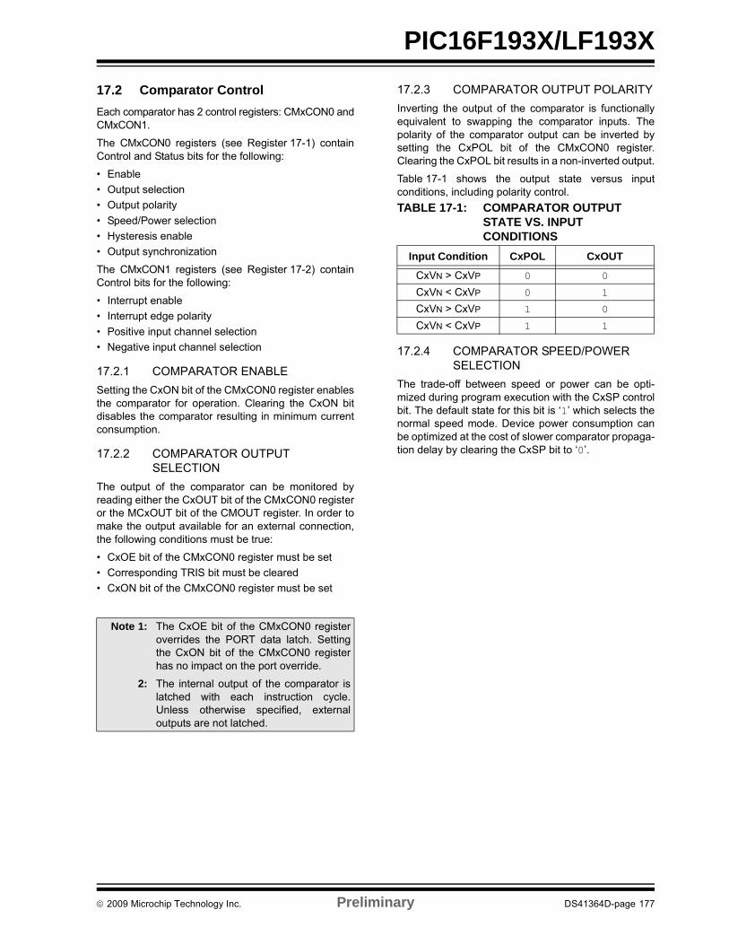
PIC16F193X/LF193X
17.2 Comparator Control
Each comparator has 2 control registers: CMxCON0 andCMxCON1.
The CMxCON0 registers (see Register 17-1) containControl and Status bits for the following:
• Enable
• Output selection
• Output polarity
• Speed/Power selection
• Hysteresis enable
• Output synchronization
The CMxCON1 registers (see Register 17-2) containControl bits for the following:
• Interrupt enable
• Interrupt edge polarity
• Positive input channel selection
• Negative input channel selection
17.2.1 COMPARATOR ENABLE
Setting the CxON bit of the CMxCON0 register enablesthe comparator for operation. Clearing the CxON bitdisables the comparator resulting in minimum currentconsumption.
17.2.2 COMPARATOR OUTPUT SELECTION
The output of the comparator can be monitored byreading either the CxOUT bit of the CMxCON0 registeror the MCxOUT bit of the CMOUT register. In order tomake the output available for an external connection,the following conditions must be true:
• CxOE bit of the CMxCON0 register must be set
• Corresponding TRIS bit must be cleared
• CxON bit of the CMxCON0 register must be set
17.2.3 COMPARATOR OUTPUT POLARITY
Inverting the output of the comparator is functionallyequivalent to swapping the comparator inputs. Thepolarity of the comparator output can be inverted bysetting the CxPOL bit of the CMxCON0 register.Clearing the CxPOL bit results in a non-inverted output.
Table 17-1 shows the output state versus inputconditions, including polarity control.
17.2.4 COMPARATOR SPEED/POWER SELECTION
The trade-off between speed or power can be opti-mized during program execution with the CxSP controlbit. The default state for this bit is ‘1’ which selects thenormal speed mode. Device power consumption canbe optimized at the cost of slower comparator propaga-tion delay by clearing the CxSP bit to ‘0’.
Note 1: The CxOE bit of the CMxCON0 registeroverrides the PORT data latch. Settingthe CxON bit of the CMxCON0 registerhas no impact on the port override.
2: The internal output of the comparator islatched with each instruction cycle.Unless otherwise specified, externaloutputs are not latched.
TABLE 17-1: COMPARATOR OUTPUT STATE VS. INPUT CONDITIONS
Input Condition CxPOL CxOUT
CxVN > CxVP 0 0
CxVN < CxVP 0 1
CxVN > CxVP 1 0
CxVN < CxVP 1 1
2009 Microchip Technology Inc. Preliminary DS41364D-page 177
PIC16F193X/LF193X
17.3 Comparator Hysteresis
A selectable amount of separation voltage can beadded to the input pins of each comparator to provide ahysteresis function to the overall operation. Hysteresisis enabled by setting the CxHYS bit of the CMxCON0register.
These hysteresis levels change as a function of thecomparator’s Speed/Power mode selection.
Table 17-2 shows the hysteresis levels.
These levels are approximate.
See Section 29.0 “Electrical Specifications” formore information.
17.4 Timer1 Gate Operation
The output resulting from a comparator operation canbe used as a source for gate control of Timer1. SeeSection 20.6 “Timer1 Gate” for more information.This feature is useful for timing the duration or intervalof an analog event.
It is recommended that the comparator output be syn-chronized to Timer1. This ensures that Timer1 does notincrement while a change in the comparator is occur-ring.
17.4.1 COMPARATOR OUTPUT SYNCHRONIZATION
The output from either comparator, C1 or C2, can besynchronized with Timer1 by setting the CxSYNC bit ofthe CMxCON0 register.
Once enabled, the comparator output is latched on thefalling edge of the Timer1 source clock. If a prescaler isused with Timer1, the comparator output is latched afterthe prescaling function. To prevent a race condition, thecomparator output is latched on the falling edge of theTimer1 clock source and Timer1 increments on therising edge of its clock source. See the ComparatorBlock Diagram (Figure 17-2) and the Timer1 BlockDiagram (Figure 21-1) for more information.
17.5 Comparator Interrupt
An interrupt can be generated upon a change in theoutput value of the comparator for each comparator, arising edge detector and a Falling edge detector arepresent.
When either edge detector is triggered and its associ-ated enable bit is set (CxINTP and/or CxINTN bits ofthe CMxCON1 register), the Corresponding InterruptFlag bit (CxIF bit of the PIR2 register) will be set.
To enable the interrupt, you must set the following bits:
• CxON, CxPOL and CxSP bits of the CMxCON0 register
• CxIE bit of the PIE2 register
• CxINTP bit of the CMxCON1 register (for a rising edge detection)
• CxINTN bit of the CMxCON1 register (for a falling edge detection)
• PEIE and GIE bits of the INTCON register
The associated interrupt flag bit, CxIF bit of the PIR2register, must be cleared in software. If another edge isdetected while this flag is being cleared, the flag will stillbe set at the end of the sequence.
17.6 Comparator Positive Input Selection
Configuring the CxPCH<1:0> bits of the CMxCON1register directs an internal voltage reference or ananalog pin to the non-inverting input of the comparator:
• CxIN+ analog pin
• DAC
• FVR (Fixed Voltage Reference)
• VSS (Ground)
See Section 14.0 “Fixed Voltage Reference (FVR)”for more information on the Fixed Voltage Referencemodule.
See Section 16.0 “Digital-to-Analog Converter(DAC) Module” for more information on the DAC inputsignal.
Any time the comparator is disabled (CxON = 0), allcomparator inputs are disabled.
TABLE 17-2: HYSTERESIS LEVELS
CxSP CxHYS Enabled CxHYS Disabled
0 ± 3mV << ± 1mV
1 ± 20mV ± 3mV
Note: Although a comparator is disabled, aninterrupt can be generated by changingthe output polarity with the CxPOL bit ofthe CMxCON0 register, or by switching thecomparator on or off with the CxON bit ofthe CMxCON0 register.
DS41364D-page 178 Preliminary 2009 Microchip Technology Inc.

PIC16F193X/LF193X
17.7 Comparator Negative Input Selection
The CxNCH<1:0> bits of the CMxCON0 register directone of four analog pins to the comparator invertinginput.
17.8 Comparator Response Time
The comparator output is indeterminate for a period oftime after the change of an input source or the selectionof a new reference voltage. This period is referred to asthe response time. The response time of the comparatordiffers from the settling time of the voltage reference.Therefore, both of these times must be considered whendetermining the total response time to a comparatorinput change. See the Comparator and Voltage Refer-ence Specifications in Section 29.0 “Electrical Speci-fications” for more details.
17.9 Interaction with ECCP Logic
The C1 and C2 comparators can be used as generalpurpose comparators. Their outputs can be broughtout to the C1OUT and C2OUT pins. When the ECCPAuto-Shutdown is active it can use one or bothcomparator signals. If auto-restart is also enabled, thecomparators can be configured as a closed loopanalog feedback to the ECCP, thereby, creating ananalog controlled PWM.
17.10 Analog Input Connection Considerations
A simplified circuit for an analog input is shown inFigure 17-3. Since the analog input pins share theirconnection with a digital input, they have reversebiased ESD protection diodes to VDD and VSS. Theanalog input, therefore, must be between VSS and VDD.If the input voltage deviates from this range by morethan 0.6V in either direction, one of the diodes is for-ward biased and a latch-up may occur.
A maximum source impedance of 10 k is recommendedfor the analog sources. Also, any external componentconnected to an analog input pin, such as a capacitor ora Zener diode, should have very little leakage current tominimize inaccuracies introduced.
FIGURE 17-3: ANALOG INPUT MODEL
Note: To use CxIN+ and CxINx- pins as analoginput, the appropriate bits must be set inthe ANSEL register and the correspondingTRIS bits must also be set to disable theoutput drivers.
Note 1: When reading a PORT register, all pinsconfigured as analog inputs will read as a‘0’. Pins configured as digital inputs willconvert as an analog input, according tothe input specification.
2: Analog levels on any pin defined as adigital input, may cause the input buffer toconsume more current than is specified.
VA
Rs < 10K
CPIN5 pF
VDD
VT 0.6V
VT 0.6V
RIC
ILEAKAGE(1)
Vss
Legend: CPIN = Input CapacitanceILEAKAGE = Leakage Current at the pin due to various junctionsRIC = Interconnect ResistanceRS = Source ImpedanceVA = Analog VoltageVT = Threshold Voltage
To Comparator
Note 1: See Section 29.0 “Electrical Specifications”
AnalogInputpin
2009 Microchip Technology Inc. Preliminary DS41364D-page 179
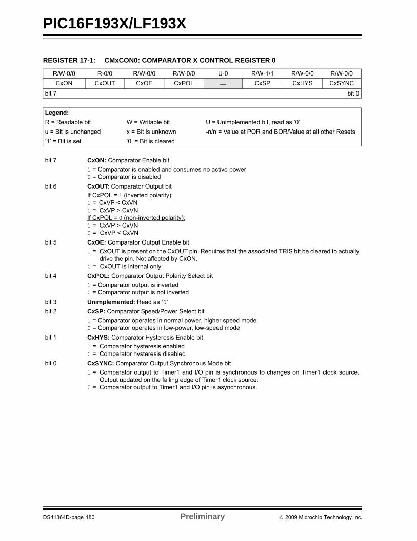
PIC16F193X/LF193X
REGISTER 17-1: CMxCON0: COMPARATOR X CONTROL REGISTER 0
R/W-0/0 R-0/0 R/W-0/0 R/W-0/0 U-0 R/W-1/1 R/W-0/0 R/W-0/0
CxON CxOUT CxOE CxPOL — CxSP CxHYS CxSYNC
bit 7 bit 0
Legend:
R = Readable bit W = Writable bit U = Unimplemented bit, read as ‘0’
u = Bit is unchanged x = Bit is unknown -n/n = Value at POR and BOR/Value at all other Resets
‘1’ = Bit is set ‘0’ = Bit is cleared
bit 7 CxON: Comparator Enable bit
1 = Comparator is enabled and consumes no active power0 = Comparator is disabled
bit 6 CxOUT: Comparator Output bit
If CxPOL = 1 (inverted polarity):1 = CxVP < CxVN0 = CxVP > CxVNIf CxPOL = 0 (non-inverted polarity):1 = CxVP > CxVN0 = CxVP < CxVN
bit 5 CxOE: Comparator Output Enable bit
1 = CxOUT is present on the CxOUT pin. Requires that the associated TRIS bit be cleared to actuallydrive the pin. Not affected by CxON.
0 = CxOUT is internal only
bit 4 CxPOL: Comparator Output Polarity Select bit
1 = Comparator output is inverted0 = Comparator output is not inverted
bit 3 Unimplemented: Read as ‘0’
bit 2 CxSP: Comparator Speed/Power Select bit
1 = Comparator operates in normal power, higher speed mode0 = Comparator operates in low-power, low-speed mode
bit 1 CxHYS: Comparator Hysteresis Enable bit
1 = Comparator hysteresis enabled0 = Comparator hysteresis disabled
bit 0 CxSYNC: Comparator Output Synchronous Mode bit
1 = Comparator output to Timer1 and I/O pin is synchronous to changes on Timer1 clock source.Output updated on the falling edge of Timer1 clock source.
0 = Comparator output to Timer1 and I/O pin is asynchronous.
DS41364D-page 180 Preliminary 2009 Microchip Technology Inc.

PIC16F193X/LF193X
REGISTER 17-2: CMxCON1: COMPARATOR CX CONTROL REGISTER 1
R/W-0/0 R/W-0/0 R/W-0/0 R/W-0/0 U-0 U-0 R/W-0/0 R/W-0/0
CxINTP CxINTN CxPCH<1:0> — — CxNCH<1:0>
bit 7 bit 0
Legend:
R = Readable bit W = Writable bit U = Unimplemented bit, read as ‘0’
u = Bit is unchanged x = Bit is unknown -n/n = Value at POR and BOR/Value at all other Resets
‘1’ = Bit is set ‘0’ = Bit is cleared
bit 7 CxINTP: Comparator Interrupt on Positive Going Edge Enable bits
1 = The CxIF interrupt flag will be set upon a positive going edge of the CxOUT bit0 = No interrupt flag will be set on a positive going edge of the CxOUT bit
bit 6 CxINTN: Comparator Interrupt on Negative Going Edge Enable bits
1 = The CxIF interrupt flag will be set upon a negative going edge of the CxOUT bit0 = No interrupt flag will be set on a negative going edge of the CxOUT bit
bit 5-4 CxPCH<1:0>: Comparator Positive Input Channel Select bits
00 = CxVP connects to CxIN+ pin01 = CxVP connects to DAC Voltage Reference10 = CxVP connects to FVR Voltage Reference11 = CxVP connects to VSS
bit 3-2 Unimplemented: Read as ‘0’
bit 1-0 CxNCH<1:0>: Comparator Negative Input Channel Select bits
00 = CxVN connects to C12IN0- pin01 = CxVN connects to C12IN1- pin10 = CxVN connects to C12IN2- pin11 = CxVN connects to C12IN3- pin
REGISTER 17-3: CMOUT: COMPARATOR OUTPUT REGISTER
U-0 U-0 U-0 U-0 U-0 U-0 R-0/0 R-0/0
— — — — — — MC2OUT MC1OUT
bit 7 bit 0
Legend:
R = Readable bit W = Writable bit U = Unimplemented bit, read as ‘0’
u = Bit is unchanged x = Bit is unknown -n/n = Value at POR and BOR/Value at all other Resets
‘1’ = Bit is set ‘0’ = Bit is cleared
bit 7-2 Unimplemented: Read as ‘0’
bit 1 MC2OUT: Mirror Copy of C2OUT bit
bit 0 MC1OUT: Mirror Copy of C1OUT bit
2009 Microchip Technology Inc. Preliminary DS41364D-page 181

PIC16F193X/LF193X
TABLE 17-3: SUMMARY OF REGISTERS ASSOCIATED WITH COMPARATOR MODULE
Name Bit 7 Bit 6 Bit 5 Bit 4 Bit 3 Bit 2 Bit 1 Bit 0Register on Page
CM1CON0 C1ON C1OUT C1OE C1POL --- C1SP C1HYS C1SYNC 180
CM2CON0 C2ON C2OUT C2OE C2POL — C2SP C2HYS C2SYNC 180
CM1CON1 C1NTP C1INTN C1PCH<1:0> — — C1NCH<1:0> 181
CM2CON1 C2NTP C2INTN C2PCH<1:0> — — C2NCH<1:0> 181
CMOUT — — — — — — MC2OUT MC1OUT 181
FVRCON FVREN FVRRDY Reserved Reserved CDAFVR<1:0> ADFVR<1:0> 154
DACCON0 DACEN DACLPS DACOE — DACPSS<1:0> — DACNSS 172
DACCON1 — — — DACR<4:0> 172
INTCON GIE PEIE TMR0IE INTE IOCIE TMR0IF INTF IOCIF 99
PIE2 OSFIE C2IE C1IE EEIE BCLIE LCDIE — CCP2IE 101
PIR2 OSFIF C2IF C1IF EEIF BCLIF LCDIF — CCP2IF 104
TRISA TRISA7 TRISA6 TRISA5 TRISA4 TRISA3 TRISA2 TRISA1 TRISA0 132
TRISB TRISB7 TRISB6 TRISB5 TRISB4 TRISB3 TRISB2 TRISB1 TRISB0 137
ANSELA — — ANSA5 ANSA4 ANSA3 ANSA2 ANSA1 ANSA0 133
ANSELB — — ANSB5 ANSB4 ANSB3 ANSB2 ANSB1 ANSB0 137
Legend: — = unimplemented location, read as ‘0’. Shaded cells are unused by the Comparator module.
DS41364D-page 182 Preliminary 2009 Microchip Technology Inc.
PIC16F193X/LF193X
18.0 SR LATCH
The module consists of a single SR Latch with multipleSet and Reset inputs as well as separate latch outputs.The SR Latch module includes the following features:
• Programmable input selection
• SR Latch output is available externally
• Separate Q and Q outputs
• Firmware Set and Reset
The SR Latch can be used in a variety of analog appli-cations, including oscillator circuits, one-shot circuit,hysteretic controllers, and analog timing applications.
18.1 Latch Operation
The latch is a Set-Reset Latch that does not depend ona clock source. Each of the Set and Reset inputs areactive-high. The latch can be Set or Reset by:
• Software control (SRPS and SRPR bits)
• Comparator C1 output (SYNCC1OUT)
• Comparator C2 output (SYNCC2OUT)
• SRI pin
• Programmable clock (SRCLK)
The SRPS and the SRPR bits of the SRCON0 registermay be used to set or reset the SR Latch, respectively.The latch is Reset-dominant. Therefore, if both Set andReset inputs are high, the latch will go to the Resetstate. Both the SRPS and SRPR bits are self resettingwhich means that a single write to either of the bits is allthat is necessary to complete a latch Set or Reset oper-ation.
The output from Comparator C1 or C2 can be used asthe Set or Reset inputs of the SR Latch. The output ofeither Comparator can be synchronized to the Timer1clock source. See Section 17.0 “Comparator Mod-ule” and Section 20.0 “Timer1 Module with GateControl” for more information.
An external source on the SRI pin can be used as theSet or Reset inputs of the SR Latch.
An internal clock source is available that can periodicallyset or reset the SR Latch. The SRCLK<2:0> bits in theSRCON0 register are used to select the clock sourceperiod. The SRSCKE and SRRCKE bits of the SRCON1register enable the clock source to set or reset the SRLatch, respectively.
18.2 Latch Output
The SRQEN and SRNQEN bits of the SRCON0 regis-ter control the Q and Q latch outputs. Both of the SRLatch outputs may be directly output to an I/O pin at thesame time. The Q latch output pin function can bemoved to an alternate pin using the SRNQSEL bit ofthe APFCON register.
The applicable TRIS bit of the corresponding port mustbe cleared to enable the port pin output driver.
18.3 Effects of a Reset
Upon any device Reset, the SR Latch output is not ini-tialized to a known state. The user’s firmware isresponsible for initializing the latch output beforeenabling the output pins.
Note: Enabling both the Set and Reset inputsfrom any one source at the same time mayresult in indeterminate operation, as theReset dominance cannot be assured.
2009 Microchip Technology Inc. Preliminary DS41364D-page 183
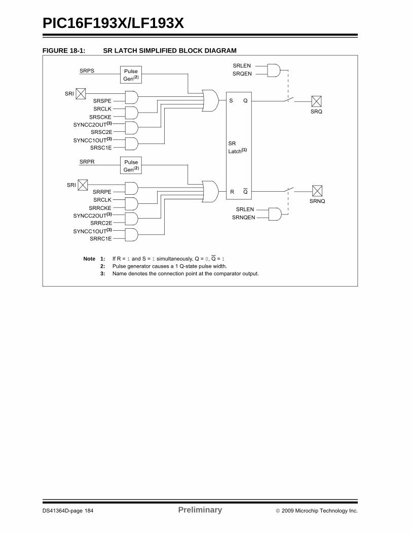
PIC16F193X/LF193X
FIGURE 18-1: SR LATCH SIMPLIFIED BLOCK DIAGRAM
SRPS
S
R
Q
Q
Note 1: If R = 1 and S = 1 simultaneously, Q = 0, Q = 12: Pulse generator causes a 1 Q-state pulse width.3: Name denotes the connection point at the comparator output.
Pulse
Gen(2)
SR
Latch(1)
SRQEN
SRSPE
SRSC2E
SRSCKE
SRCLK
SYNCC2OUT(3)
SRSC1ESYNCC1OUT(3)
SRPR Pulse
Gen(2)
SRRPE
SRRC2E
SRRCKE
SRCLK
SYNCC2OUT(3)
SRRC1ESYNCC1OUT(3)
SRLEN
SRNQEN
SRLEN
SRQ
SRNQ
SRI
SRI
DS41364D-page 184 Preliminary 2009 Microchip Technology Inc.

PIC16F193X/LF193X
TABLE 18-1: SRCLK FREQUENCY TABLE
SRCLK Divider FOSC = 32 MHz FOSC = 20 MHz FOSC = 16 MHz FOSC = 4 MHz FOSC = 1 MHz
111 512 62.5 kHz 39.0 kHz 31.3 kHz 7.81 kHz 1.95 kHz
110 256 125 kHz 78.1 kHz 62.5 kHz 15.6 kHz 3.90 kHz
101 128 250 kHz 156 kHz 125 kHz 31.25 kHz 7.81 kHz
100 64 500 kHz 313 kHz 250 kHz 62.5 kHz 15.6 kHz
011 32 1 MHz 625 kHz 500 kHz 125 kHz 31.3 kHz
010 16 2 MHz 1.25 MHz 1 MHz 250 kHz 62.5 kHz
001 8 4 MHz 2.5 MHz 2 MHz 500 kHz 125 kHz
000 4 8 MHz 5 MHz 4 MHz 1 MHz 250 kHz
REGISTER 18-1: SRCON0: SR LATCH CONTROL 0 REGISTER
R/W-0/0 R/W-0/0 R/W-0/0 R/W-0/0 R/W-0/0 R/W-0/0 R/S-0/0 R/S-0/0
SRLEN SRCLK<2:0> SRQEN SRNQEN SRPS SRPR
bit 7 bit 0
Legend:
R = Readable bit W = Writable bit U = Unimplemented bit, read as ‘0’
u = Bit is unchanged x = Bit is unknown -n/n = Value at POR and BOR/Value at all other Resets
‘1’ = Bit is set ‘0’ = Bit is cleared S = Bit is set only
bit 7 SRLEN: SR Latch Enable bit1 = SR Latch is enabled0 = SR Latch is disabled
bit 6-4 SRCLK<2:0>: SR Latch Clock Divider bits000 = Generates a 1 FOSC wide pulse every 4th FOSC cycle clock001 = Generates a 1 FOSC wide pulse every 8th FOSC cycle clock010 = Generates a 1 FOSC wide pulse every 16th FOSC cycle clock011 = Generates a 1 FOSC wide pulse every 32nd FOSC cycle clock100 = Generates a 1 FOSC wide pulse every 64th FOSC cycle clock101 = Generates a 1 FOSC wide pulse every 128th FOSC cycle clock110 = Generates a 1 FOSC wide pulse every 256th FOSC cycle clock111 = Generates a 1 FOSC wide pulse every 512th FOSC cycle clock
bit 3 SRQEN: SR Latch Q Output Enable bitIf SRLEN = 1:
1 = Q is present on the SRQ pin0 = External Q output is disabled
If SRLEN = 0:SR Latch is disabled
bit 2 SRNQEN: SR Latch Q Output Enable bitIf SRLEN = 1:
1 = Q is present on the SRnQ pin0 = External Q output is disabled
If SRLEN = 0:SR Latch is disabled
bit 1 SRPS: Pulse Set Input of the SR Latch bit(1)
1 = Pulse set input for 1 Q-clock period0 = No effect on set input.
bit 0 SRPR: Pulse Reset Input of the SR Latch bit(1)
1 = Pulse reset input for 1 Q-clock period0 = No effect on reset input.
Note 1: Set only, always reads back ‘0’.
2009 Microchip Technology Inc. Preliminary DS41364D-page 185

PIC16F193X/LF193X
REGISTER 18-2: SRCON1: SR LATCH CONTROL 1 REGISTER
R/W-0/0 R/W-0/0 R/W-0/0 R/W-0/0 R/W-0/0 R/W-0/0 R/W-0/0 R/W-0/0
SRSPE SRSCKE SRSC2E SRSC1E SRRPE SRRCKE SRRC2E SRRC1E
bit 7 bit 0
Legend:
R = Readable bit W = Writable bit U = Unimplemented bit, read as ‘0’
u = Bit is unchanged x = Bit is unknown -n/n = Value at POR and BOR/Value at all other Resets
‘1’ = Bit is set ‘0’ = Bit is cleared
bit 7 SRSPE: SR Latch Peripheral Set Enable bit
1 = SR Latch is set when the SRI pin is high.0 = SRI pin has no effect on the set input of the SR Latch
bit 6 SRSCKE: SR Latch Set Clock Enable bit
1 = Set input of SR Latch is pulsed with SRCLK 0 = SRCLK has no effect on the set input of the SR Latch
bit 5 SRSC2E: SR Latch C2 Set Enable bit
1 = SR Latch is set when the C2 Comparator output is high0 = C2 Comparator output has no effect on the set input of the SR Latch
bit 4 SRSC1E: SR Latch C1 Set Enable bit
1 = SR Latch is set when the C1 Comparator output is high0 = C1 Comparator output has no effect on the set input of the SR Latch
bit 3 SRRPE: SR Latch Peripheral Reset Enable bit
1 = SR Latch is reset when the SRI pin is high.0 = SRI pin has no effect on the reset input of the SR Latch
bit 2 SRRCKE: SR Latch Reset Clock Enable bit
1 = Reset input of SR Latch is pulsed with SRCLK 0 = SRCLK has no effect on the reset input of the SR Latch
bit 1 SRRC2E: SR Latch C2 Reset Enable bit
1 = SR Latch is reset when the C2 Comparator output is high0 = C2 Comparator output has no effect on the reset input of the SR Latch
bit 0 SRRC1E: SR Latch C1 Reset Enable bit
1 = SR Latch is reset when the C1 Comparator output is high0 = C1 Comparator output has no effect on the reset input of the SR Latch
DS41364D-page 186 Preliminary 2009 Microchip Technology Inc.

PIC16F193X/LF193X
TABLE 18-2: SUMMARY OF REGISTERS ASSOCIATED WITH SR LATCH MODULE
Name Bit 7 Bit 6 Bit 5 Bit 4 Bit 3 Bit 2 Bit 1 Bit 0Register on Page
ANSELA — — ANSA5 ANSA4 ANSA3 ANSA2 ANSA1 ANSA0 133
SRCON0 SRLEN SRCLK<2:0> SRQEN SRNQEN SRPS SRPR 185
SRCON1 SRSPE SRSCKE SRSC2E SRSC1E SRRPE SRRCKE SRRC2E SRRC1E 186
TRISA TRISA7 TRISA6 TRISA5 TRISA4 TRISA3 TRISA2 TRISA1 TRISA0 132
Legend: — = unimplemented location, read as ‘0’. Shaded cells are unused by the SR Latch module.
2009 Microchip Technology Inc. Preliminary DS41364D-page 187

PIC16F193X/LF193X
NOTES:
DS41364D-page 188 Preliminary 2009 Microchip Technology Inc.
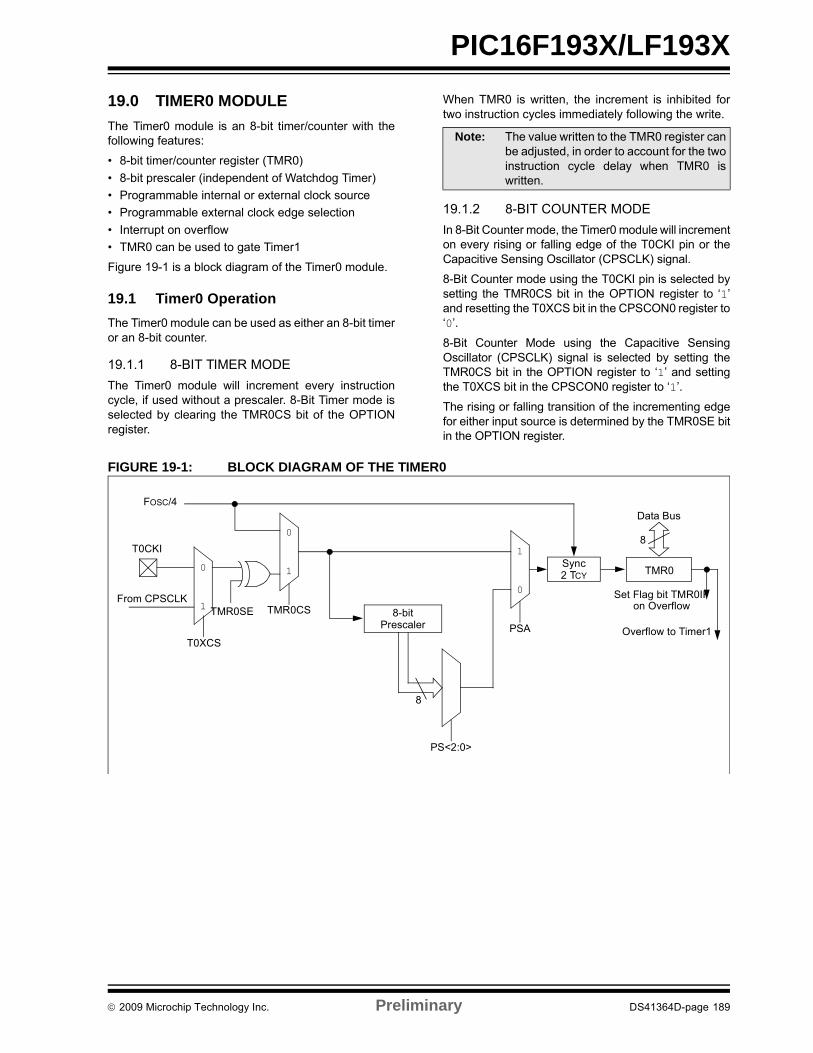
PIC16F193X/LF193X
19.0 TIMER0 MODULE
The Timer0 module is an 8-bit timer/counter with thefollowing features:
• 8-bit timer/counter register (TMR0)
• 8-bit prescaler (independent of Watchdog Timer)
• Programmable internal or external clock source
• Programmable external clock edge selection
• Interrupt on overflow
• TMR0 can be used to gate Timer1
Figure 19-1 is a block diagram of the Timer0 module.
19.1 Timer0 Operation
The Timer0 module can be used as either an 8-bit timeror an 8-bit counter.
19.1.1 8-BIT TIMER MODE
The Timer0 module will increment every instructioncycle, if used without a prescaler. 8-Bit Timer mode isselected by clearing the TMR0CS bit of the OPTIONregister.
When TMR0 is written, the increment is inhibited fortwo instruction cycles immediately following the write.
19.1.2 8-BIT COUNTER MODE
In 8-Bit Counter mode, the Timer0 module will incrementon every rising or falling edge of the T0CKI pin or theCapacitive Sensing Oscillator (CPSCLK) signal.
8-Bit Counter mode using the T0CKI pin is selected bysetting the TMR0CS bit in the OPTION register to ‘1’and resetting the T0XCS bit in the CPSCON0 register to‘0’.
8-Bit Counter Mode using the Capacitive SensingOscillator (CPSCLK) signal is selected by setting theTMR0CS bit in the OPTION register to ‘1’ and settingthe T0XCS bit in the CPSCON0 register to ‘1’.
The rising or falling transition of the incrementing edgefor either input source is determined by the TMR0SE bitin the OPTION register.
FIGURE 19-1: BLOCK DIAGRAM OF THE TIMER0
Note: The value written to the TMR0 register canbe adjusted, in order to account for the twoinstruction cycle delay when TMR0 iswritten.
T0CKI
TMR0SE
TMR0
PS<2:0>
Data Bus
Set Flag bit TMR0IFon OverflowTMR0CS
0
1
0
18
8
8-bitPrescaler
FOSC/4
PSA
Sync2 TCY
Overflow to Timer1
1
0
From CPSCLK
T0XCS
2009 Microchip Technology Inc. Preliminary DS41364D-page 189

PIC16F193X/LF193X
19.1.3 SOFTWARE PROGRAMMABLE PRESCALER
A software programmable prescaler is available forexclusive use with Timer0. The prescaler is enabled byclearing the PSA bit of the OPTION register.
There are 8 prescaler options for the Timer0 moduleranging from 1:2 to 1:256. The prescale values areselectable via the PS<2:0> bits of the OPTION register.In order to have a 1:1 prescaler value for the Timer0module, the prescaler must be disabled by setting thePSA bit of the OPTION register.
The prescaler is not readable or writable. All instructionswriting to the TMR0 register will clear the prescaler.
19.1.4 TIMER0 INTERRUPT
Timer0 will generate an interrupt when the TMR0register overflows from FFh to 00h. The TMR0IFinterrupt flag bit of the INTCON register is set everytime the TMR0 register overflows, regardless ofwhether or not the Timer0 interrupt is enabled. TheTMR0IF bit can only be cleared in software. The Timer0interrupt enable is the TMR0IE bit of the INTCONregister.
19.1.5 8-BIT COUNTER MODE SYNCHRONIZATION
When in 8-Bit Counter mode, the incrementing edge onthe T0CKI pin must be synchronized to the instructionclock. Synchronization can be accomplished bysampling the prescaler output on the Q2 and Q4 cyclesof the instruction clock. The high and low periods of theexternal clocking source must meet the timingrequirements as shown in Section 29.0 “ElectricalSpecifications”.
19.1.6 OPERATION DURING SLEEP
Timer0 cannot operate while the processor is in Sleepmode. The contents of the TMR0 register will remainunchanged while the processor is in Sleep mode.
Note: The Watchdog Timer (WDT) uses its ownindependent prescaler.
Note: The Timer0 interrupt cannot wake theprocessor from Sleep since the timer isfrozen during Sleep.
DS41364D-page 190 Preliminary 2009 Microchip Technology Inc.
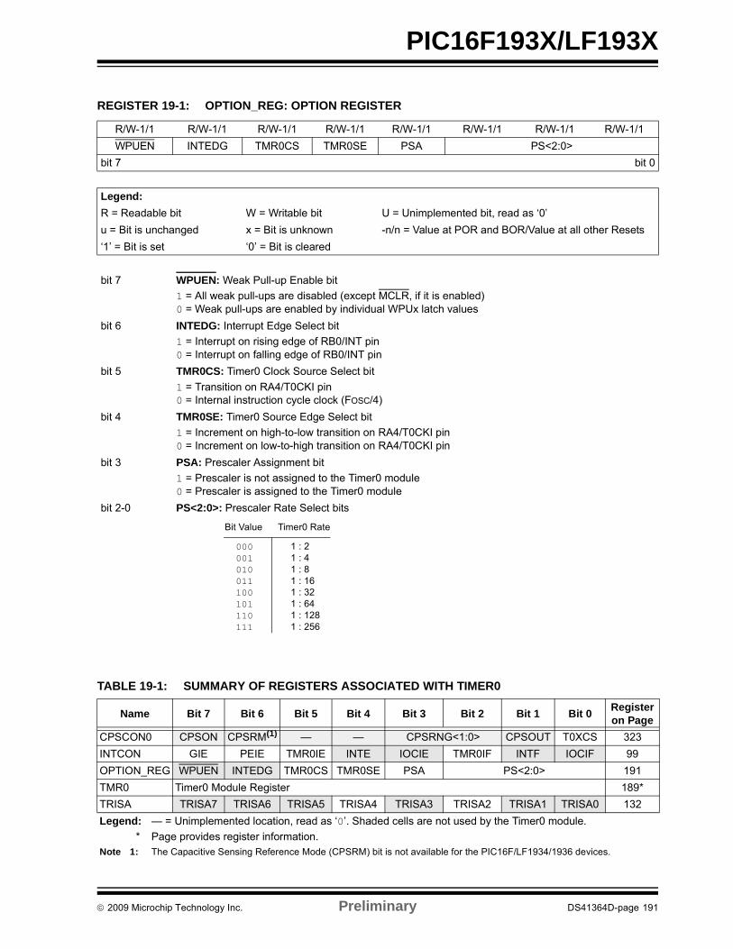
PIC16F193X/LF193X
TABLE 19-1: SUMMARY OF REGISTERS ASSOCIATED WITH TIMER0
REGISTER 19-1: OPTION_REG: OPTION REGISTER
R/W-1/1 R/W-1/1 R/W-1/1 R/W-1/1 R/W-1/1 R/W-1/1 R/W-1/1 R/W-1/1
WPUEN INTEDG TMR0CS TMR0SE PSA PS<2:0>
bit 7 bit 0
Legend:
R = Readable bit W = Writable bit U = Unimplemented bit, read as ‘0’
u = Bit is unchanged x = Bit is unknown -n/n = Value at POR and BOR/Value at all other Resets
‘1’ = Bit is set ‘0’ = Bit is cleared
bit 7 WPUEN: Weak Pull-up Enable bit
1 = All weak pull-ups are disabled (except MCLR, if it is enabled)0 = Weak pull-ups are enabled by individual WPUx latch values
bit 6 INTEDG: Interrupt Edge Select bit
1 = Interrupt on rising edge of RB0/INT pin0 = Interrupt on falling edge of RB0/INT pin
bit 5 TMR0CS: Timer0 Clock Source Select bit
1 = Transition on RA4/T0CKI pin0 = Internal instruction cycle clock (FOSC/4)
bit 4 TMR0SE: Timer0 Source Edge Select bit
1 = Increment on high-to-low transition on RA4/T0CKI pin0 = Increment on low-to-high transition on RA4/T0CKI pin
bit 3 PSA: Prescaler Assignment bit
1 = Prescaler is not assigned to the Timer0 module0 = Prescaler is assigned to the Timer0 module
bit 2-0 PS<2:0>: Prescaler Rate Select bits
000001010011100101110111
1 : 21 : 41 : 81 : 161 : 321 : 641 : 1281 : 256
Bit Value Timer0 Rate
Name Bit 7 Bit 6 Bit 5 Bit 4 Bit 3 Bit 2 Bit 1 Bit 0Register on Page
CPSCON0 CPSON CPSRM(1) — — CPSRNG<1:0> CPSOUT T0XCS 323
INTCON GIE PEIE TMR0IE INTE IOCIE TMR0IF INTF IOCIF 99
OPTION_REG WPUEN INTEDG TMR0CS TMR0SE PSA PS<2:0> 191
TMR0 Timer0 Module Register 189*
TRISA TRISA7 TRISA6 TRISA5 TRISA4 TRISA3 TRISA2 TRISA1 TRISA0 132
Legend: — = Unimplemented location, read as ‘0’. Shaded cells are not used by the Timer0 module.
* Page provides register information.Note 1: The Capacitive Sensing Reference Mode (CPSRM) bit is not available for the PIC16F/LF1934/1936 devices.
2009 Microchip Technology Inc. Preliminary DS41364D-page 191

PIC16F193X/LF193X
NOTES:
DS41364D-page 192 Preliminary 2009 Microchip Technology Inc.

PIC16F193X/LF193X
20.0 TIMER1 MODULE WITH GATE CONTROL
The Timer1 module is a 16-bit timer/counter with thefollowing features:
• 16-bit timer/counter register pair (TMR1H:TMR1L)
• Programmable internal or external clock source
• 2-bit prescaler
• Dedicated 32 kHz oscillator circuit
• Optionally synchronized comparator out
• Multiple Timer1 gate (count enable) sources
• Interrupt on overflow
• Wake-up on overflow (external clock, Asynchronous mode only)
• Time base for the Capture/Compare function
• Special Event Trigger (with CCP/ECCP)
• Selectable Gate Source Polarity
• Gate Toggle Mode
• Gate Single-pulse Mode
• Gate Value Status
• Gate Event Interrupt
Figure 20-1 is a block diagram of the Timer1 module.
FIGURE 20-1: TIMER1 BLOCK DIAGRAM
TMR1H TMR1L
T1SYNC
T1CKPS<1:0>
Prescaler1, 2, 4, 8
0
1
Synchronizedclock input
2
Set flag bitTMR1IF onOverflow TMR1(2)
TMR1ON
Note 1: ST Buffer is high speed type when using T1CKI.2: Timer1 register increments on rising edge.3: Synchronize does not operate while in Sleep.
T1G
T1OSC
FOSC/4Internal
Clock
T1OSO
T1OSI
T1OSCEN
1
0
T1CKI
TMR1CS<1:0>
(1)
Synchronize(3)
det
Sleep input
TMR1GE
0
1
00
01
10
11
T1GPOL
D
QCK
Q
0
1
T1GVAL
T1GTM
Single Pulse
Acq. Control
T1GSPM
T1GGO/DONE
T1GSS<1:0>
EN
OUT
10
11
00
01FOSC
InternalClock
Cap. Sensing
R
D
EN
Q
Q1RD
T1GCON
Data Bus
det
Interrupt
TMR1GIF
Set
T1CLK
FOSC/2InternalClock
D
EN
Q
T1G_IN
TMR1ON
Oscillator
From Timer0
Comparator 1
Overflow
Comparator 2SYNCC2OUT
SYNCC1OUT
To Comparator Module
To LCD and Clock Switching Modules
2009 Microchip Technology Inc. Preliminary DS41364D-page 193
PIC16F193X/LF193X
20.1 Timer1 Operation
The Timer1 module is a 16-bit incrementing counterwhich is accessed through the TMR1H:TMR1L registerpair. Writes to TMR1H or TMR1L directly update thecounter.
When used with an internal clock source, the module isa timer and increments on every instruction cycle.When used with an external clock source, the modulecan be used as either a timer or counter and incre-ments on every selected edge of the external source.
Timer1 is enabled by configuring the TMR1ON andTMR1GE bits in the T1CON and T1GCON registers,respectively. Table 20-1 displays the Timer1 enableselections.
20.2 Clock Source Selection
The TMR1CS<1:0> and T1OSCEN bits of the T1CONregister are used to select the clock source for Timer1.Table 20-2 displays the clock source selections.
20.2.1 INTERNAL CLOCK SOURCE
When the internal clock source is selected theTMR1H:TMR1L register pair will increment on multiplesof FOSC as determined by the Timer1 prescaler.
When the FOSC internal clock source is selected, theTimer1 register value will increment by four counts everyinstruction clock cycle. Due to this condition, a 2 LSBerror in resolution will occur when reading the Timer1value. To utilize the full resolution of Timer1, anasynchronous input signal must be used to gate theTimer1 clock input.
The following asynchronous sources may be used:
• Asynchronous event on the T1G pin to Timer1 Gate
• C1 or C2 comparator input to Timer1 Gate
20.2.2 EXTERNAL CLOCK SOURCE
When the external clock source is selected, the Timer1module may work as a timer or a counter.
When enabled to count, Timer1 is incremented on therising edge of the external clock input T1CKI or thecapacitive sensing oscillator signal. Either of theseexternal clock sources can be synchronized to themicrocontroller system clock or they can runasynchronously.
When used as a timer with a clock oscillator, anexternal 32.768 kHz crystal can be used in conjunctionwith the dedicated internal oscillator circuit.
TABLE 20-1: TIMER1 ENABLE SELECTIONS
TMR1ON TMR1GETimer1
Operation
0 0 Off
0 1 Off
1 0 Always On
1 1 Count Enabled
Note: In Counter mode, a falling edge must beregistered by the counter prior to the firstincrementing rising edge after any one ormore of the following conditions:
• Timer1 enabled after POR
• Write to TMR1H or TMR1L
• Timer1 is disabled
• Timer1 is disabled (TMR1ON = 0) when T1CKI is high then Timer1 is enabled (TMR1ON=1) when T1CKI is low.
TABLE 20-2: CLOCK SOURCE SELECTIONS
TMR1CS1 TMR1CS0 T1OSCEN Clock Source
0 1 x System Clock (FOSC)
0 0 x Instruction Clock (FOSC/4)
1 1 x Capacitive Sensing Oscillator
1 0 0 External Clocking on T1CKI Pin
1 0 1 Osc.Circuit On T1OSI/T1OSO Pins
DS41364D-page 194 Preliminary 2009 Microchip Technology Inc.
PIC16F193X/LF193X
20.3 Timer1 Prescaler
Timer1 has four prescaler options allowing 1, 2, 4 or 8divisions of the clock input. The T1CKPS bits of theT1CON register control the prescale counter. Theprescale counter is not directly readable or writable;however, the prescaler counter is cleared upon a write toTMR1H or TMR1L.
20.4 Timer1 Oscillator
A dedicated low-power 32.768 kHz oscillator circuit isbuilt-in between pins T1OSI (input) and T1OSO(amplifier output). This internal circuit is to be used inconjunction with an external 32.768 kHz crystal.
The oscillator circuit is enabled by setting theT1OSCEN bit of the T1CON register. The oscillator willcontinue to run during Sleep.
20.5 Timer1 Operation in Asynchronous Counter Mode
If control bit T1SYNC of the T1CON register is set, theexternal clock input is not synchronized. The timerincrements asynchronously to the internal phaseclocks. If external clock source is selected then thetimer will continue to run during Sleep and cangenerate an interrupt on overflow, which will wake-upthe processor. However, special precautions insoftware are needed to read/write the timer (seeSection 20.5.1 “Reading and Writing Timer1 inAsynchronous Counter Mode”).
20.5.1 READING AND WRITING TIMER1 IN ASYNCHRONOUS COUNTER MODE
Reading TMR1H or TMR1L while the timer is runningfrom an external asynchronous clock will ensure a validread (taken care of in hardware). However, the usershould keep in mind that reading the 16-bit timer in two8-bit values itself, poses certain problems, since thetimer may overflow between the reads.
For writes, it is recommended that the user simply stopthe timer and write the desired values. A writecontention may occur by writing to the timer registers,while the register is incrementing. This may produce anunpredictable value in the TMR1H:TMR1L register pair.
20.6 Timer1 Gate
Timer1 can be configured to count freely or the countcan be enabled and disabled using Timer1 Gatecircuitry. This is also referred to as Timer1 Gate Enable.
Timer1 Gate can also be driven by multiple selectablesources.
20.6.1 TIMER1 GATE ENABLE
The Timer1 Gate Enable mode is enabled by settingthe TMR1GE bit of the T1GCON register. The polarityof the Timer1 Gate Enable mode is configured usingthe T1GPOL bit of the T1GCON register.
When Timer1 Gate Enable mode is enabled, Timer1will increment on the rising edge of the Timer1 clocksource. When Timer1 Gate Enable mode is disabled,no incrementing will occur and Timer1 will hold thecurrent count. See Figure 20-3 for timing details.
20.6.2 TIMER1 GATE SOURCE SELECTION
The Timer1 Gate source can be selected from one offour different sources. Source selection is controlled bythe T1GSS bits of the T1GCON register. The polarityfor each available source is also selectable. Polarityselection is controlled by the T1GPOL bit of theT1GCON register.
TABLE 20-4: TIMER1 GATE SOURCES
Note: The oscillator requires a start-up andstabilization time before use. Thus,T1OSCEN should be set and a suitabledelay observed prior to enabling Timer1.
Note: When switching from synchronous toasynchronous operation, it is possible toskip an increment. When switching fromasynchronous to synchronous operation,it is possible to produce an additionalincrement.
TABLE 20-3: TIMER1 GATE ENABLE SELECTIONS
T1CLK T1GPOL T1G Timer1 Operation
0 0 Counts
0 1 Holds Count
1 0 Holds Count
1 1 Counts
T1GSS Timer1 Gate Source
00 Timer1 Gate Pin
01 Overflow of Timer0(TMR0 increments from FFh to 00h)
10 Comparator 1 Output SYNCC1OUT(optionally Timer1 synchronized output)
11 Comparator 2 Output SYNCC2OUT(optionally Timer1 synchronized output)
2009 Microchip Technology Inc. Preliminary DS41364D-page 195
PIC16F193X/LF193X
20.6.2.1 T1G Pin Gate Operation
The T1G pin is one source for Timer1 Gate Control. Itcan be used to supply an external source to the Timer1Gate circuitry.
20.6.2.2 Timer0 Overflow Gate Operation
When Timer0 increments from FFh to 00h, alow-to-high pulse will automatically be generated andinternally supplied to the Timer1 Gate circuitry.
20.6.2.3 Comparator C1 Gate Operation
The output resulting from a Comparator 1 operation canbe selected as a source for Timer1 Gate Control. TheComparator 1 output (SYNCC1OUT) can besynchronized to the Timer1 clock or left asynchronous.For more information see Section 17.4.1 “ComparatorOutput Synchronization”.
20.6.2.4 Comparator C2 Gate Operation
The output resulting from a Comparator 2 operationcan be selected as a source for Timer1 Gate Control.The Comparator 2 output (SYNCC2OUT) can besynchronized to the Timer1 clock or left asynchronous.For more information see Section 17.4.1 “ComparatorOutput Synchronization”.
20.6.3 TIMER1 GATE TOGGLE MODE
When Timer1 Gate Toggle mode is enabled, it is possi-ble to measure the full-cycle length of a Timer1 gatesignal, as opposed to the duration of a single levelpulse.
The Timer1 Gate source is routed through a flip-flopthat changes state on every incrementing edge of thesignal. See Figure 20-4 for timing details.
Timer1 Gate Toggle mode is enabled by setting theT1GTM bit of the T1GCON register. When the T1GTMbit is cleared, the flip-flop is cleared and held clear. Thisis necessary in order to control which edge ismeasured.
20.6.4 TIMER1 GATE SINGLE-PULSE MODE
When Timer1 Gate Single-Pulse mode is enabled, it ispossible to capture a single pulse gate event. Timer1Gate Single-Pulse mode is first enabled by setting theT1GSPM bit in the T1GCON register. Next, theT1GGO/DONE bit in the T1GCON register must be set.The Timer1 will be fully enabled on the nextincrementing edge. On the next trailing edge of thepulse, the T1GGO/DONE bit will automatically becleared. No other gate events will be allowed toincrement Timer1 until the T1GGO/DONE bit is onceagain set in software.
Clearing the T1GSPM bit of the T1GCON register willalso clear the T1GGO/DONE bit. See Figure 20-5 fortiming details.
Enabling the Toggle mode and the Single-Pulse modesimultaneously will permit both sections to worktogether. This allows the cycle times on the Timer1Gate source to be measured. See Figure 20-6 fortiming details.
20.6.5 TIMER1 GATE VALUE STATUS
When Timer1 Gate Value Status is utilized, it is possibleto read the most current level of the gate control value.The value is stored in the T1GVAL bit in the T1GCONregister. The T1GVAL bit is valid even when the Timer1Gate is not enabled (TMR1GE bit is cleared).
20.6.6 TIMER1 GATE EVENT INTERRUPT
When Timer1 Gate Event Interrupt is enabled, it is pos-sible to generate an interrupt upon the completion of agate event. When the falling edge of T1GVAL occurs,the TMR1GIF flag bit in the PIR1 register will be set. Ifthe TMR1GIE bit in the PIE1 register is set, then aninterrupt will be recognized.
The TMR1GIF flag bit operates even when the Timer1Gate is not enabled (TMR1GE bit is cleared).
Note: Enabling Toggle mode at the same time aschanging the gate polarity may result inindeterminate operation.
DS41364D-page 196 Preliminary 2009 Microchip Technology Inc.

PIC16F193X/LF193X
20.7 Timer1 Interrupt
The Timer1 register pair (TMR1H:TMR1L) incrementsto FFFFh and rolls over to 0000h. When Timer1 rollsover, the Timer1 interrupt flag bit of the PIR1 register isset. To enable the interrupt on rollover, you must setthese bits:
• TMR1ON bit of the T1CON register
• TMR1IE bit of the PIE1 register
• PEIE bit of the INTCON register
• GIE bit of the INTCON register
The interrupt is cleared by clearing the TMR1IF bit inthe Interrupt Service Routine.
20.8 Timer1 Operation During Sleep
Timer1 can only operate during Sleep when setup inAsynchronous Counter mode. In this mode, an externalcrystal or clock source can be used to increment thecounter. To set up the timer to wake the device:
• TMR1ON bit of the T1CON register must be set
• TMR1IE bit of the PIE1 register must be set
• PEIE bit of the INTCON register must be set
• T1SYNC bit of the T1CON register must be set
• TMR1CS bits of the T1CON register must be configured
• T1OSCEN bit of the T1CON register must be configured
The device will wake-up on an overflow and executethe next instructions. If the GIE bit of the INTCONregister is set, the device will call the Interrupt ServiceRoutine.
Timer1 oscillator will continue to operate in Sleepregardless of the T1SYNC bit setting.
20.9 ECCP/CCP Capture/Compare Time Base
The CCP modules use the TMR1H:TMR1L registerpair as the time base when operating in Capture orCompare mode.
In Capture mode, the value in the TMR1H:TMR1Lregister pair is copied into the CCPR1H:CCPR1Lregister pair on a configured event.
In Compare mode, an event is triggered when the valueCCPR1H:CCPR1L register pair matches the value inthe TMR1H:TMR1L register pair. This event can be aSpecial Event Trigger.
For more information, see Section 12.0 “I/O Ports”.
20.10 ECCP/CCP Special Event Trigger
When any of the CCP’s are configured to trigger a spe-cial event, the trigger will clear the TMR1H:TMR1L reg-ister pair. This special event does not cause a Timer1interrupt. The CCP module may still be configured togenerate a CCP interrupt.
In this mode of operation, the CCPR1H:CCPR1Lregister pair becomes the period register for Timer1.
Timer1 should be synchronized and FOSC/4 should beselected as the clock source in order to utilize the Spe-cial Event Trigger. Asynchronous operation of Timer1can cause a Special Event Trigger to be missed.
In the event that a write to TMR1H or TMR1L coincideswith a Special Event Trigger from the CCP, the write willtake precedence.
For more information, see Section 15.2.5 “SpecialEvent Trigger”.
FIGURE 20-2: TIMER1 INCREMENTING EDGE
Note: The TMR1H:TMR1L register pair and theTMR1IF bit should be cleared beforeenabling interrupts.
T1CKI = 1
when TMR1Enabled
T1CKI = 0
when TMR1Enabled
Note 1: Arrows indicate counter increments.
2: In Counter mode, a falling edge must be registered by the counter prior to the first incrementing rising edge of the clock.
2009 Microchip Technology Inc. Preliminary DS41364D-page 197
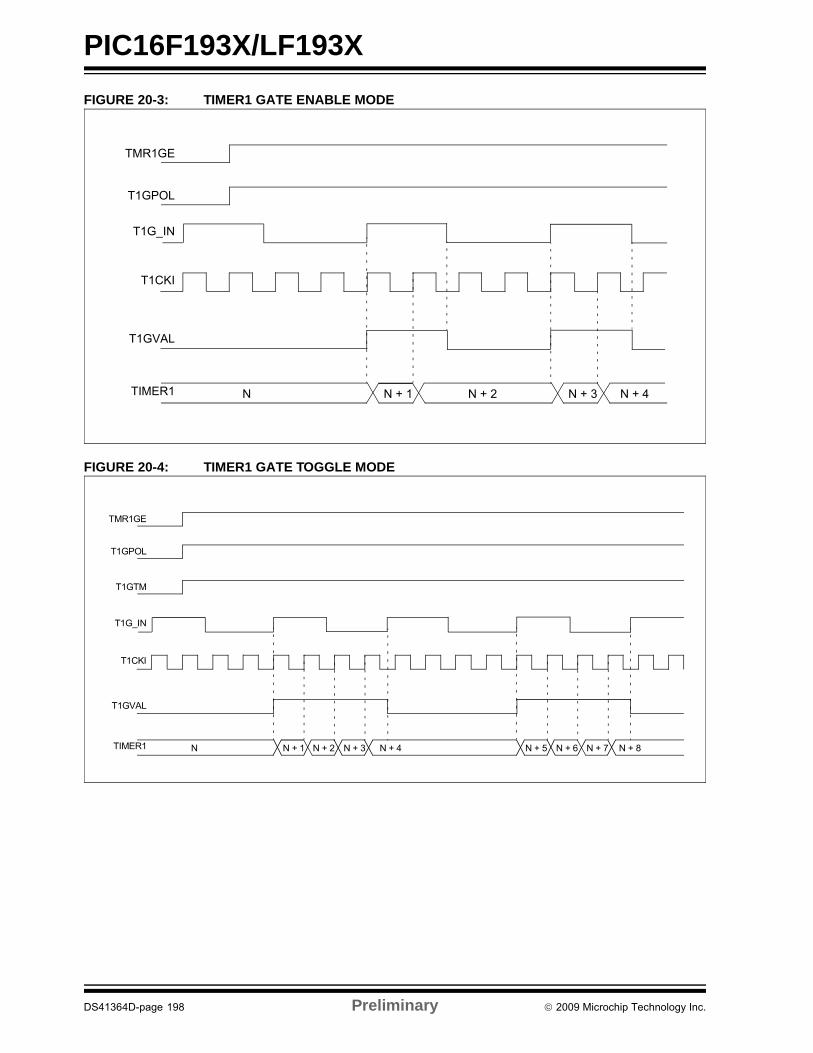
PIC16F193X/LF193X
FIGURE 20-3: TIMER1 GATE ENABLE MODE
FIGURE 20-4: TIMER1 GATE TOGGLE MODE
TMR1GE
T1GPOL
T1G_IN
T1CKI
T1GVAL
TIMER1 N N + 1 N + 2 N + 3 N + 4
TMR1GE
T1GPOL
T1GTM
T1G_IN
T1CKI
T1GVAL
TIMER1 N N + 1 N + 2 N + 3 N + 4 N + 5 N + 6 N + 7 N + 8
DS41364D-page 198 Preliminary 2009 Microchip Technology Inc.
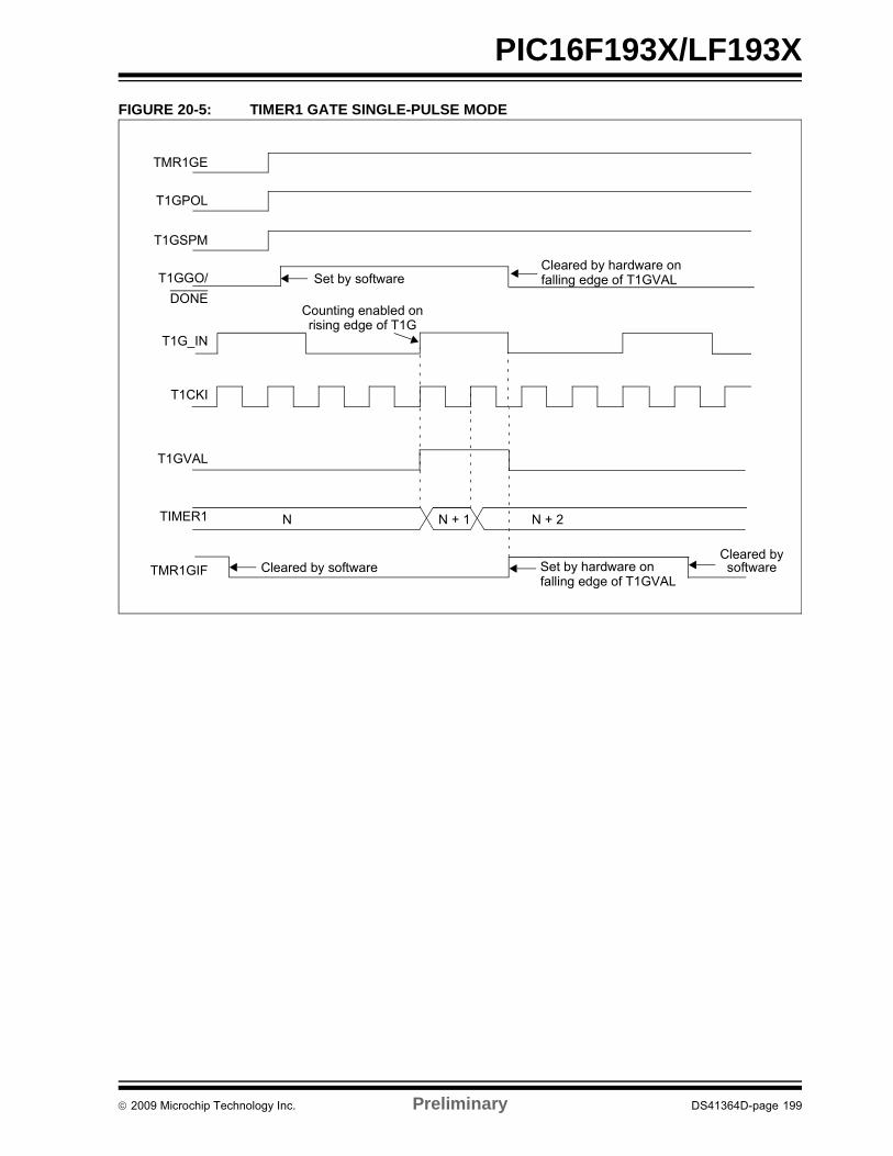
PIC16F193X/LF193X
FIGURE 20-5: TIMER1 GATE SINGLE-PULSE MODE
TMR1GE
T1GPOL
T1G_IN
T1CKI
T1GVAL
TIMER1 N N + 1 N + 2
T1GSPM
T1GGO/
DONE
Set by softwareCleared by hardware onfalling edge of T1GVAL
Set by hardware onfalling edge of T1GVAL
Cleared by softwareCleared bysoftwareTMR1GIF
Counting enabled onrising edge of T1G
2009 Microchip Technology Inc. Preliminary DS41364D-page 199
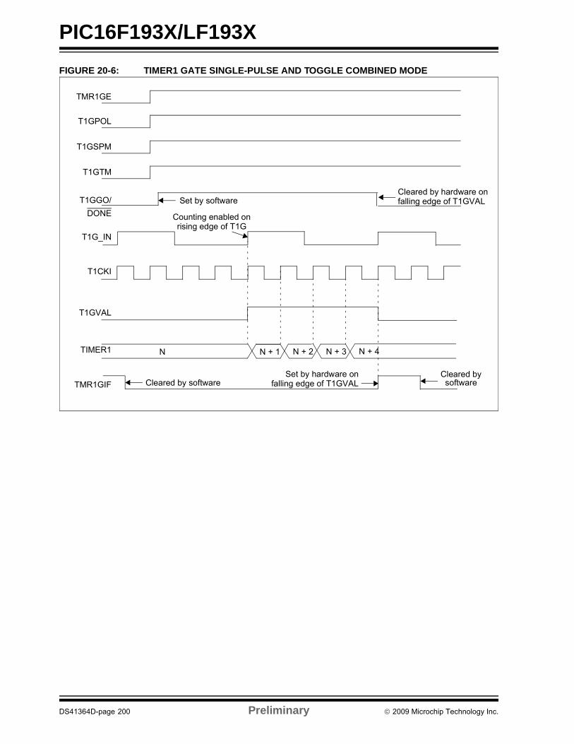
PIC16F193X/LF193X
FIGURE 20-6: TIMER1 GATE SINGLE-PULSE AND TOGGLE COMBINED MODE
TMR1GE
T1GPOL
T1G_IN
T1CKI
T1GVAL
TIMER1 N N + 1 N + 2
T1GSPM
T1GGO/
DONE
Set by softwareCleared by hardware onfalling edge of T1GVAL
Set by hardware onfalling edge of T1GVALCleared by software
Cleared bysoftwareTMR1GIF
T1GTM
Counting enabled onrising edge of T1G
N + 4N + 3
DS41364D-page 200 Preliminary 2009 Microchip Technology Inc.

PIC16F193X/LF193X
20.11 Timer1 Control Register
The Timer1 Control register (T1CON), shown inRegister 20-1, is used to control Timer1 and select thevarious features of the Timer1 module.
REGISTER 20-1: T1CON: TIMER1 CONTROL REGISTER
R/W-0/u R/W-0/u R/W-0/u R/W-0/u R/W-0/u R/W-0/u U-0 R/W-0/u
TMR1CS<1:0> T1CKPS<1:0> T1OSCEN T1SYNC — TMR1ON
bit 7 bit 0
Legend:
R = Readable bit W = Writable bit U = Unimplemented bit, read as ‘0’
u = Bit is unchanged x = Bit is unknown -n/n = Value at POR and BOR/Value at all other Resets
‘1’ = Bit is set ‘0’ = Bit is cleared
bit 7-6 TMR1CS<1:0>: Timer1 Clock Source Select bits
11 = Timer1 clock source is Capacitive Sensing Oscillator (CAPOSC)10 = Timer1 clock source is pin or oscillator:
If T1OSCEN = 0:External clock from T1CKI pin (on the rising edge)If T1OSCEN = 1:Crystal oscillator on T1OSI/T1OSO pins
01 = Timer1 clock source is system clock (FOSC)00 = Timer1 clock source is instruction clock (FOSC/4)
bit 5-4 T1CKPS<1:0>: Timer1 Input Clock Prescale Select bits
11 = 1:8 Prescale value10 = 1:4 Prescale value01 = 1:2 Prescale value00 = 1:1 Prescale value
bit 3 T1OSCEN: LP Oscillator Enable Control bit
1 = Dedicated Timer1 oscillator circuit enabled0 = Dedicated Timer1 oscillator circuit disabled
bit 2 T1SYNC: Timer1 External Clock Input Synchronization Control bit
TMR1CS<1:0> = 1X1 = Do not synchronize external clock input0 = Synchronize external clock input with system clock (FOSC)
TMR1CS<1:0> = 0XThis bit is ignored. Timer1 uses the internal clock when TMR1CS<1:0> = 1X.
bit 1 Unimplemented: Read as ‘0’
bit 0 TMR1ON: Timer1 On bit
1 = Enables Timer10 = Stops Timer1
Clears Timer1 Gate flip-flop
2009 Microchip Technology Inc. Preliminary DS41364D-page 201
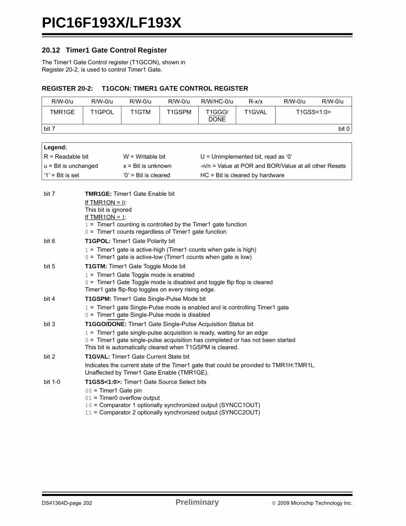
PIC16F193X/LF193X
20.12 Timer1 Gate Control Register
The Timer1 Gate Control register (T1GCON), shown inRegister 20-2, is used to control Timer1 Gate.
REGISTER 20-2: T1GCON: TIMER1 GATE CONTROL REGISTER
R/W-0/u R/W-0/u R/W-0/u R/W-0/u R/W/HC-0/u R-x/x R/W-0/u R/W-0/u
TMR1GE T1GPOL T1GTM T1GSPM T1GGO/DONE
T1GVAL T1GSS<1:0>
bit 7 bit 0
Legend:
R = Readable bit W = Writable bit U = Unimplemented bit, read as ‘0’
u = Bit is unchanged x = Bit is unknown -n/n = Value at POR and BOR/Value at all other Resets
‘1’ = Bit is set ‘0’ = Bit is cleared HC = Bit is cleared by hardware
bit 7 TMR1GE: Timer1 Gate Enable bit
If TMR1ON = 0:This bit is ignoredIf TMR1ON = 1:1 = Timer1 counting is controlled by the Timer1 gate function0 = Timer1 counts regardless of Timer1 gate function
bit 6 T1GPOL: Timer1 Gate Polarity bit
1 = Timer1 gate is active-high (Timer1 counts when gate is high)0 = Timer1 gate is active-low (Timer1 counts when gate is low)
bit 5 T1GTM: Timer1 Gate Toggle Mode bit
1 = Timer1 Gate Toggle mode is enabled0 = Timer1 Gate Toggle mode is disabled and toggle flip flop is clearedTimer1 gate flip-flop toggles on every rising edge.
bit 4 T1GSPM: Timer1 Gate Single-Pulse Mode bit
1 = Timer1 gate Single-Pulse mode is enabled and is controlling Timer1 gate0 = Timer1 gate Single-Pulse mode is disabled
bit 3 T1GGO/DONE: Timer1 Gate Single-Pulse Acquisition Status bit
1 = Timer1 gate single-pulse acquisition is ready, waiting for an edge0 = Timer1 gate single-pulse acquisition has completed or has not been startedThis bit is automatically cleared when T1GSPM is cleared.
bit 2 T1GVAL: Timer1 Gate Current State bit
Indicates the current state of the Timer1 gate that could be provided to TMR1H:TMR1L.Unaffected by Timer1 Gate Enable (TMR1GE).
bit 1-0 T1GSS<1:0>: Timer1 Gate Source Select bits
00 = Timer1 Gate pin01 = Timer0 overflow output10 = Comparator 1 optionally synchronized output (SYNCC1OUT)11 = Comparator 2 optionally synchronized output (SYNCC2OUT)
DS41364D-page 202 Preliminary 2009 Microchip Technology Inc.
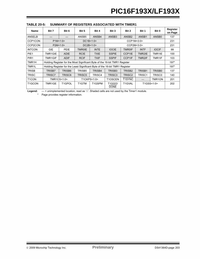
PIC16F193X/LF193X
TABLE 20-5: SUMMARY OF REGISTERS ASSOCIATED WITH TIMER1
Name Bit 7 Bit 6 Bit 5 Bit 4 Bit 3 Bit 2 Bit 1 Bit 0Register on Page
ANSELB — — ANSB5 ANSB4 ANSB3 ANSB2 ANSB1 ANSB0 137
CCP1CON P1M<1:0> DC1B<1:0> CCP1M<3:0> 231
CCP2CON P2M<1:0> DC2B<1:0> CCP2M<3:0> 231
INTCON GIE PEIE TMR0IE INTE IOCIE TMR0IF INTF IOCIF 99
PIE1 TMR1GIE ADIE RCIE TXIE SSPIE CCP1IE TMR2IE TMR1IE 100
PIR1 TMR1GIF ADIF RCIF TXIF SSPIF CCP1IF TMR2IF TMR1IF 103
TMR1H Holding Register for the Most Significant Byte of the 16-bit TMR1 Register 197*
TMR1L Holding Register for the Least Significant Byte of the 16-bit TMR1 Register 197*
TRISB TRISB7 TRISB6 TRISB5 TRISB4 TRISB3 TRISB2 TRISB1 TRISB0 137
TRISC TRISC7 TRISC6 TRISC5 TRISC4 TRISC3 TRISC2 TRISC1 TRISC0 140
T1CON TMR1CS<1:0> T1CKPS<1:0> T1OSCEN T1SYNC — TMR1ON 201
T1GCON TMR1GE T1GPOL T1GTM T1GSPM T1GGO/DONE
T1GVAL T1GSS<1:0> 202
Legend: — = unimplemented location, read as ‘0’. Shaded cells are not used by the Timer1 module.* Page provides register information.
2009 Microchip Technology Inc. Preliminary DS41364D-page 203

PIC16F193X/LF193X
NOTES:
DS41364D-page 204 Preliminary 2009 Microchip Technology Inc.
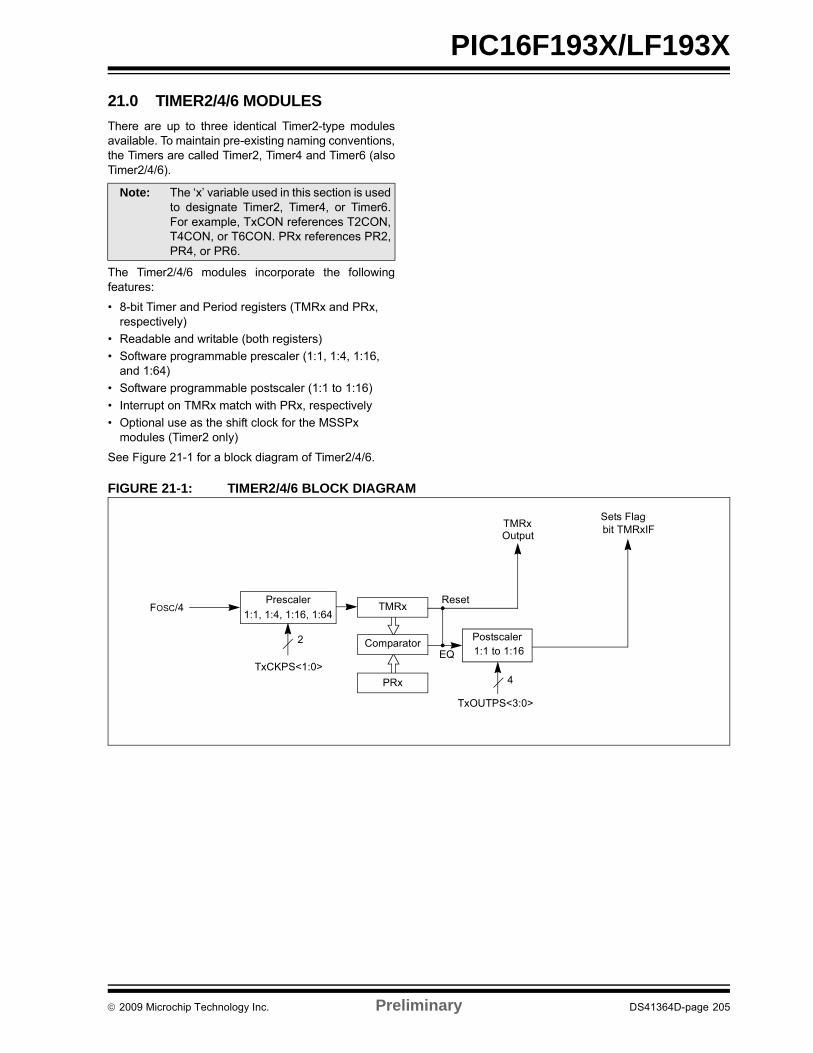
PIC16F193X/LF193X
21.0 TIMER2/4/6 MODULES
There are up to three identical Timer2-type modulesavailable. To maintain pre-existing naming conventions,the Timers are called Timer2, Timer4 and Timer6 (alsoTimer2/4/6).
The Timer2/4/6 modules incorporate the followingfeatures:
• 8-bit Timer and Period registers (TMRx and PRx, respectively)
• Readable and writable (both registers)
• Software programmable prescaler (1:1, 1:4, 1:16, and 1:64)
• Software programmable postscaler (1:1 to 1:16)
• Interrupt on TMRx match with PRx, respectively
• Optional use as the shift clock for the MSSPx modules (Timer2 only)
See Figure 21-1 for a block diagram of Timer2/4/6.
FIGURE 21-1: TIMER2/4/6 BLOCK DIAGRAM
Note: The ‘x’ variable used in this section is usedto designate Timer2, Timer4, or Timer6.For example, TxCON references T2CON,T4CON, or T6CON. PRx references PR2,PR4, or PR6.
Comparator
TMRxSets Flag
TMRx
Output
Reset
Postscaler
Prescaler
PRx
2
FOSC/4
1:1 to 1:16
1:1, 1:4, 1:16, 1:64
EQ
4
bit TMRxIF
TxOUTPS<3:0>
TxCKPS<1:0>
2009 Microchip Technology Inc. Preliminary DS41364D-page 205
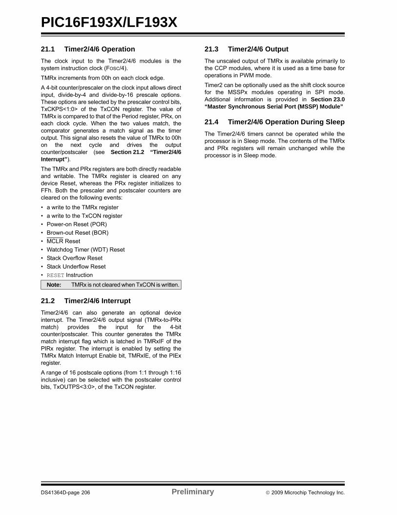
PIC16F193X/LF193X
21.1 Timer2/4/6 Operation
The clock input to the Timer2/4/6 modules is thesystem instruction clock (FOSC/4).
TMRx increments from 00h on each clock edge.
A 4-bit counter/prescaler on the clock input allows directinput, divide-by-4 and divide-by-16 prescale options.These options are selected by the prescaler control bits,TxCKPS<1:0> of the TxCON register. The value ofTMRx is compared to that of the Period register, PRx, oneach clock cycle. When the two values match, thecomparator generates a match signal as the timeroutput. This signal also resets the value of TMRx to 00hon the next cycle and drives the outputcounter/postscaler (see Section 21.2 “Timer2/4/6Interrupt”).
The TMRx and PRx registers are both directly readableand writable. The TMRx register is cleared on anydevice Reset, whereas the PRx register initializes toFFh. Both the prescaler and postscaler counters arecleared on the following events:
• a write to the TMRx register
• a write to the TxCON register
• Power-on Reset (POR)
• Brown-out Reset (BOR)
• MCLR Reset
• Watchdog Timer (WDT) Reset
• Stack Overflow Reset
• Stack Underflow Reset
• RESET Instruction
21.2 Timer2/4/6 Interrupt
Timer2/4/6 can also generate an optional deviceinterrupt. The Timer2/4/6 output signal (TMRx-to-PRxmatch) provides the input for the 4-bitcounter/postscaler. This counter generates the TMRxmatch interrupt flag which is latched in TMRxIF of thePIRx register. The interrupt is enabled by setting theTMRx Match Interrupt Enable bit, TMRxIE, of the PIExregister.
A range of 16 postscale options (from 1:1 through 1:16inclusive) can be selected with the postscaler controlbits, TxOUTPS<3:0>, of the TxCON register.
21.3 Timer2/4/6 Output
The unscaled output of TMRx is available primarily tothe CCP modules, where it is used as a time base foroperations in PWM mode.
Timer2 can be optionally used as the shift clock sourcefor the MSSPx modules operating in SPI mode.Additional information is provided in Section 23.0“Master Synchronous Serial Port (MSSP) Module”
21.4 Timer2/4/6 Operation During Sleep
The Timer2/4/6 timers cannot be operated while theprocessor is in Sleep mode. The contents of the TMRxand PRx registers will remain unchanged while theprocessor is in Sleep mode.
Note: TMRx is not cleared when TxCON is written.
DS41364D-page 206 Preliminary 2009 Microchip Technology Inc.
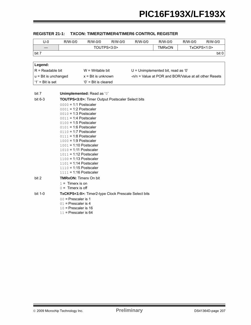
PIC16F193X/LF193X
REGISTER 21-1: TXCON: TIMER2/TIMER4/TIMER6 CONTROL REGISTER
U-0 R/W-0/0 R/W-0/0 R/W-0/0 R/W-0/0 R/W-0/0 R/W-0/0 R/W-0/0
— TOUTPS<3:0> TMRxON TxCKPS<1:0>
bit 7 bit 0
Legend:
R = Readable bit W = Writable bit U = Unimplemented bit, read as ‘0’
u = Bit is unchanged x = Bit is unknown -n/n = Value at POR and BOR/Value at all other Resets
‘1’ = Bit is set ‘0’ = Bit is cleared
bit 7 Unimplemented: Read as ‘0’
bit 6-3 TOUTPS<3:0>: Timer Output Postscaler Select bits
0000 = 1:1 Postscaler0001 = 1:2 Postscaler0010 = 1:3 Postscaler0011 = 1:4 Postscaler0100 = 1:5 Postscaler0101 = 1:6 Postscaler0110 = 1:7 Postscaler0111 = 1:8 Postscaler1000 = 1:9 Postscaler1001 = 1:10 Postscaler1010 = 1:11 Postscaler1011 = 1:12 Postscaler1100 = 1:13 Postscaler1101 = 1:14 Postscaler1110 = 1:15 Postscaler1111 = 1:16 Postscaler
bit 2 TMRxON: Timerx On bit
1 = Timerx is on0 = Timerx is off
bit 1-0 TxCKPS<1:0>: Timer2-type Clock Prescale Select bits
00 = Prescaler is 101 = Prescaler is 410 = Prescaler is 1611 = Prescaler is 64
2009 Microchip Technology Inc. Preliminary DS41364D-page 207
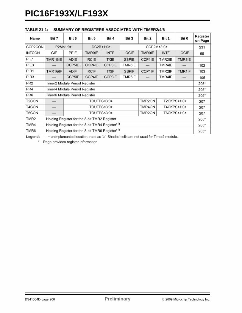
PIC16F193X/LF193X
TABLE 21-1: SUMMARY OF REGISTERS ASSOCIATED WITH TIMER2/4/6
Name Bit 7 Bit 6 Bit 5 Bit 4 Bit 3 Bit 2 Bit 1 Bit 0Register on Page
CCP2CON P2M<1:0> DC2B<1:0> CCP2M<3:0> 231
INTCON GIE PEIE TMR0IE INTE IOCIE TMR0IF INTF IOCIF 99
PIE1 TMR1GIE ADIE RCIE TXIE SSPIE CCP1IE TMR2IE TMR1IE
PIE3 — CCP5IE CCP4IE CCP3IE TMR6IE — TMR4IE — 102
PIR1 TMR1GIF ADIF RCIF TXIF SSPIF CCP1IF TMR2IF TMR1IF 103
PIR3 — CCP5IF CCP4IF CCP3IF TMR6IF — TMR4IF — 105
PR2 Timer2 Module Period Register 205*
PR4 Timer4 Module Period Register 205*
PR6 Timer6 Module Period Register 205*
T2CON — TOUTPS<3:0> TMR2ON T2CKPS<1:0> 207
T4CON — TOUTPS<3:0> TMR4ON T4CKPS<1:0> 207
T6CON — TOUTPS<3:0> TMR2ON T6CKPS<1:0> 207
TMR2 Holding Register for the 8-bit TMR2 Register 205*
TMR4 Holding Register for the 8-bit TMR4 Register(1) 205*
TMR6 Holding Register for the 8-bit TMR6 Register(1) 205*
Legend: — = unimplemented location, read as ‘0’. Shaded cells are not used for Timer2 module.
* Page provides register information.
DS41364D-page 208 Preliminary 2009 Microchip Technology Inc.
PIC16F193X/LF193X
22.0 CAPTURE/COMPARE/PWM MODULES
The Capture/Compare/PWM module is a peripheralwhich allows the user to time and control differentevents, and to generate Pulse-Width Modulation(PWM) signals. In Capture mode, the peripheral allowsthe timing of the duration of an event. The Comparemode allows the user to trigger an external event whena predetermined amount of time has expired. ThePWM mode can generate Pulse-Width Modulatedsignals of varying frequency and duty cycle.
This family of devices contains three EnhancedCapture/Compare/PWM modules (ECCP1, ECCP2,and ECCP3) and two standard Capture/Compare/PWMmodules (CCP4 and CCP5).
The Capture and Compare functions are identical for allfive CCP modules (ECCP1, ECCP2, ECCP3, CCP4,and CCP5). The only differences between CCPmodules are in the Pulse-Width Modulation (PWM)function. The standard PWM function is identical inmodules, CCP4 and CCP5. In CCP modules ECCP1,ECCP2, and ECCP3, the Enhanced PWM function hasslight variations from one another. Full-Bridge ECCPmodules have four available I/O pins while Half-BridgeECCP modules only have two available I/O pins. SeeTable 22-1 for more information.
Note 1: In devices with more than one CCPmodule, it is very important to pay closeattention to the register names used. Anumber placed after the module acronymis used to distinguish between separatemodules. For example, the CCP1CONand CCP2CON control the sameoperational aspects of two completelydifferent CCP modules.
2: Throughout this section, genericreferences to a CCP module in any of itsoperating modes may be interpreted asbeing equally applicable to ECCP1,ECCP2, ECCP3, CCP4 and CCP5.Register names, module signals, I/O pins,and bit names may use the genericdesignator ‘x’ to indicate the use of anumeral to distinguish a particular module,when required.
TABLE 22-1: PWM RESOURCES
Device Name ECCP1 ECCP2 ECCP3 CCP4 CCP5
PIC16F/LF1933/36/38Enhanced PWM
Full-BridgeEnhanced PWM
Half-BridgeEnhanced PWM
Half-BridgeStandard PWM Standard PWM
PIC16F/LF1934/37/39Enhanced PWM
Full-BridgeEnhanced PWM
Full-BridgeEnhanced PWM
Half-BridgeStandard PWM Standard PWM
2009 Microchip Technology Inc. Preliminary DS41364D-page 209
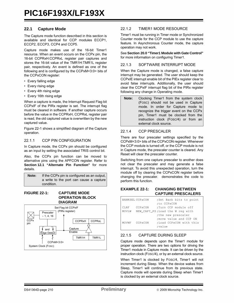
PIC16F193X/LF193X
22.1 Capture Mode
The Capture mode function described in this section isavailable and identical for CCP modules ECCP1,ECCP2, ECCP3, CCP4 and CCP5.
Capture mode makes use of the 16-bit Timer1resource. When an event occurs on the CCPx pin, the16-bit CCPRxH:CCPRxL register pair captures andstores the 16-bit value of the TMR1H:TMR1L registerpair, respectively. An event is defined as one of thefollowing and is configured by the CCPxM<3:0> bits ofthe CCPxCON register:
• Every falling edge
• Every rising edge
• Every 4th rising edge
• Every 16th rising edge
When a capture is made, the Interrupt Request Flag bitCCPxIF of the PIRx register is set. The interrupt flagmust be cleared in software. If another capture occursbefore the value in the CCPRxH, CCPRxL register pairis read, the old captured value is overwritten by the newcaptured value.
Figure 22-1 shows a simplified diagram of the Captureoperation.
22.1.1 CCP PIN CONFIGURATION
In Capture mode, the CCPx pin should be configuredas an input by setting the associated TRIS control bit.
Also, the CCPx pin function can be moved toalternative pins using the APFCON register. Refer toSection 12.1 “Alternate Pin Function” for moredetails.
FIGURE 22-1: CAPTURE MODE OPERATION BLOCK DIAGRAM
22.1.2 TIMER1 MODE RESOURCE
Timer1 must be running in Timer mode or SynchronizedCounter mode for the CCP module to use the capturefeature. In Asynchronous Counter mode, the captureoperation may not work.
See Section 20.0 “Timer1 Module with Gate Control”for more information on configuring Timer1.
22.1.3 SOFTWARE INTERRUPT MODE
When the Capture mode is changed, a false captureinterrupt may be generated. The user should keep theCCPxIE interrupt enable bit of the PIEx register clear toavoid false interrupts. Additionally, the user shouldclear the CCPxIF interrupt flag bit of the PIRx registerfollowing any change in Operating mode.
22.1.4 CCP PRESCALER
There are four prescaler settings specified by theCCPxM<3:0> bits of the CCPxCON register. Wheneverthe CCP module is turned off, or the CCP module is notin Capture mode, the prescaler counter is cleared. AnyReset will clear the prescaler counter.
Switching from one capture prescaler to another doesnot clear the prescaler and may generate a falseinterrupt. To avoid this unexpected operation, turn themodule off by clearing the CCPxCON register beforechanging the prescaler. demonstrates the code toperform this function.
EXAMPLE 22-1: CHANGING BETWEEN CAPTURE PRESCALERS
22.1.5 CAPTURE DURING SLEEP
Capture mode depends upon the Timer1 module forproper operation. There are two options for driving theTimer1 module in Capture mode. It can be driven by theinstruction clock (FOSC/4), or by an external clock source.
When Timer1 is clocked by FOSC/4, Timer1 will notincrement during Sleep. When the device wakes fromSleep, Timer1 will continue from its previous state.Capture mode will operate during Sleep when Timer1is clocked by an external clock source.
Note: If the CCPx pin is configured as an output,a write to the port can cause a capturecondition.
CCPRxH CCPRxL
TMR1H TMR1L
Set Flag bit CCPxIF(PIRx register)
CaptureEnable
CCPxM<3:0>
Prescaler 1, 4, 16
andEdge Detect
pinCCPx
System Clock (FOSC)
Note: Clocking Timer1 from the system clock(FOSC) should not be used in Capturemode. In order for Capture mode torecognize the trigger event on the CCPxpin, Timer1 must be clocked from theinstruction clock (FOSC/4) or from anexternal clock source.
BANKSEL CCPxCON ;Set Bank bits to point;to CCPxCON
CLRF CCPxCON ;Turn CCP module offMOVLW NEW_CAPT_PS;Load the W reg with
;the new prescaler;move value and CCP ON
MOVWF CCPxCON ;Load CCPxCON with this;value
DS41364D-page 210 Preliminary 2009 Microchip Technology Inc.
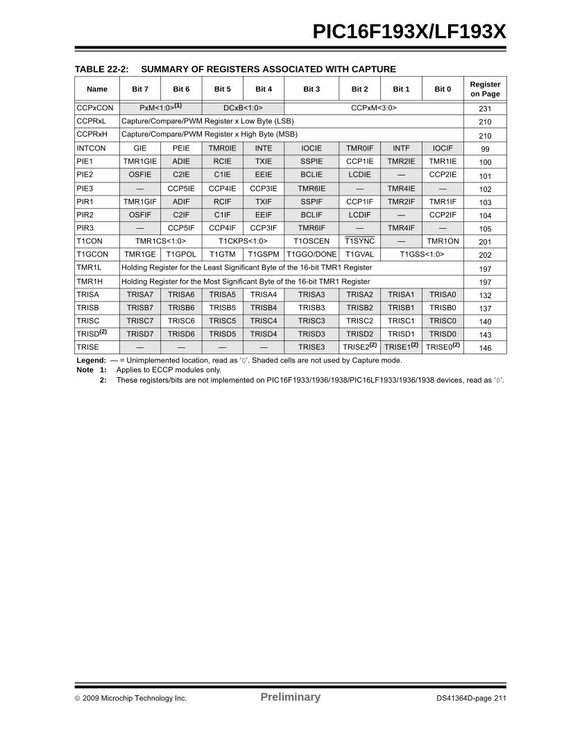
PIC16F193X/LF193X
TABLE 22-2: SUMMARY OF REGISTERS ASSOCIATED WITH CAPTURE
Name Bit 7 Bit 6 Bit 5 Bit 4 Bit 3 Bit 2 Bit 1 Bit 0Register on Page
CCPxCON PxM<1:0>(1) DCxB<1:0> CCPxM<3:0> 231
CCPRxL Capture/Compare/PWM Register x Low Byte (LSB) 210
CCPRxH Capture/Compare/PWM Register x High Byte (MSB) 210
INTCON GIE PEIE TMR0IE INTE IOCIE TMR0IF INTF IOCIF 99
PIE1 TMR1GIE ADIE RCIE TXIE SSPIE CCP1IE TMR2IE TMR1IE 100
PIE2 OSFIE C2IE C1IE EEIE BCLIE LCDIE — CCP2IE 101
PIE3 — CCP5IE CCP4IE CCP3IE TMR6IE — TMR4IE — 102
PIR1 TMR1GIF ADIF RCIF TXIF SSPIF CCP1IF TMR2IF TMR1IF 103
PIR2 OSFIF C2IF C1IF EEIF BCLIF LCDIF — CCP2IF 104
PIR3 — CCP5IF CCP4IF CCP3IF TMR6IF — TMR4IF — 105
T1CON TMR1CS<1:0> T1CKPS<1:0> T1OSCEN T1SYNC — TMR1ON 201
T1GCON TMR1GE T1GPOL T1GTM T1GSPM T1GGO/DONE T1GVAL T1GSS<1:0> 202
TMR1L Holding Register for the Least Significant Byte of the 16-bit TMR1 Register 197
TMR1H Holding Register for the Most Significant Byte of the 16-bit TMR1 Register 197
TRISA TRISA7 TRISA6 TRISA5 TRISA4 TRISA3 TRISA2 TRISA1 TRISA0 132
TRISB TRISB7 TRISB6 TRISB5 TRISB4 TRISB3 TRISB2 TRISB1 TRISB0 137
TRISC TRISC7 TRISC6 TRISC5 TRISC4 TRISC3 TRISC2 TRISC1 TRISC0 140
TRISD(2) TRISD7 TRISD6 TRISD5 TRISD4 TRISD3 TRISD2 TRISD1 TRISD0 143
TRISE — — — — TRISE3 TRISE2(2) TRISE1(2) TRISE0(2) 146
Legend: — = Unimplemented location, read as ‘0’. Shaded cells are not used by Capture mode.Note 1: Applies to ECCP modules only.
2: These registers/bits are not implemented on PIC16F1933/1936/1938/PIC16LF1933/1936/1938 devices, read as ‘0’.
2009 Microchip Technology Inc. Preliminary DS41364D-page 211

PIC16F193X/LF193X
22.2 Compare Mode
The Compare mode function described in this sectionis available and identical for CCP modules ECCP1,ECCP2, ECCP3, CCP4 and CCP5.
Compare mode makes use of the 16-bit Timer1resource. The 16-bit value of the CCPRxH:CCPRxLregister pair is constantly compared against the 16-bitvalue of the TMR1H:TMR1L register pair. When amatch occurs, one of the following events can occur:
• Toggle the CCPx output
• Set the CCPx output
• Clear the CCPx output
• Generate a Special Event Trigger
• Generate a Software Interrupt
The action on the pin is based on the value of theCCPxM<3:0> control bits of the CCPxCON register. Atthe same time, the interrupt flag CCPxIF bit is set.
All Compare modes can generate an interrupt.
Figure 22-2 shows a simplified diagram of theCompare operation.
FIGURE 22-2: COMPARE MODE OPERATION BLOCK DIAGRAM
22.2.1 CCP PIN CONFIGURATION
The user must configure the CCPx pin as an output byclearing the associated TRIS bit.
Also, the CCPx pin function can be moved toalternative pins using the APFCON register. Refer toSection 12.1 “Alternate Pin Function” for moredetails.
22.2.2 TIMER1 MODE RESOURCE
In Compare mode, Timer1 must be running in eitherTimer mode or Synchronized Counter mode. Thecompare operation may not work in AsynchronousCounter mode.
See Section 20.0 “Timer1 Module with Gate Control”for more information on configuring Timer1.
22.2.3 SOFTWARE INTERRUPT MODE
When Generate Software Interrupt mode is chosen(CCPxM<3:0> = 1010), the CCPx module does notassert control of the CCPx pin (see the CCPxCONregister).
22.2.4 SPECIAL EVENT TRIGGER
When Special Event Trigger mode is chosen(CCPxM<3:0> = 1011), the CCPx module does thefollowing:
• Resets Timer1
• Starts an ADC conversion if ADC is enabled (CCP5 only)
The CCPx module does not assert control of the CCPxpin in this mode.
The Special Event Trigger output of the CCP occursimmediately upon a match between the TMR1H,TMR1L register pair and the CCPRxH, CCPRxLregister pair. The TMR1H, TMR1L register pair is notreset until the next rising edge of the Timer1 clock. TheSpecial Event Trigger output starts an A/D conversion(if the A/D module is enabled). This feature is onlyavailable on CCP5. This allows the CCPRxH, CCPRxLregister pair to effectively provide a 16-bitprogrammable period register for Timer1.
Note: Clearing the CCPxCON register will forcethe CCPx compare output latch to thedefault low level. This is not the PORT I/Odata latch.
CCPRxH CCPRxL
TMR1H TMR1L
ComparatorQ S
R
OutputLogic
Special Event Trigger
Set CCPxIF Interrupt Flag(PIRx)
Match
TRIS
CCPxM<3:0>Mode Select
Output Enable
Pin
Special Event Trigger will:
• CCP1-CCP4: Reset Timer1, but not set interrupt flag bit TMR1IF.
• CCP5: Reset Timer1, but not set interrupt flag bit and set bit GO/DONE (ADCON0<1>).
CCPx 4
Note: Clocking Timer1 from the system clock(FOSC) should not be used in Capturemode. In order for Capture mode torecognize the trigger event on the CCPxpin, TImer1 must be clocked from theinstruction clock (FOSC/4) or from anexternal clock source.
Note 1: The Special Event Trigger from the CCPmodule does not set interrupt flag bitTMR1IF of the PIR1 register.
2: Removing the match condition bychanging the contents of the CCPRxHand CCPRxL register pair, between theclock edge that generates the SpecialEvent Trigger and the clock edge thatgenerates the Timer1 Reset, will precludethe Reset from occurring.
DS41364D-page 212 Preliminary 2009 Microchip Technology Inc.
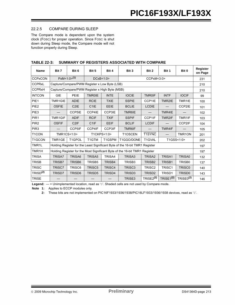
PIC16F193X/LF193X
22.2.5 COMPARE DURING SLEEP
The Compare mode is dependent upon the systemclock (FOSC) for proper operation. Since FOSC is shutdown during Sleep mode, the Compare mode will notfunction properly during Sleep.
TABLE 22-3: SUMMARY OF REGISTERS ASSOCIATED WITH COMPARE
Name Bit 7 Bit 6 Bit 5 Bit 4 Bit 3 Bit 2 Bit 1 Bit 0Register on Page
CCPxCON PxM<1:0>(1) DCxB<1:0> CCPxM<3:0> 231
CCPRxL Capture/Compare/PWM Register x Low Byte (LSB) 210
CCPRxH Capture/Compare/PWM Register x High Byte (MSB) 210
INTCON GIE PEIE TMR0IE INTE IOCIE TMR0IF INTF IOCIF 99
PIE1 TMR1GIE ADIE RCIE TXIE SSPIE CCP1IE TMR2IE TMR1IE 100
PIE2 OSFIE C2IE C1IE EEIE BCLIE LCDIE — CCP2IE 101
PIE3 — CCP5IE CCP4IE CCP3IE TMR6IE — TMR4IE — 102
PIR1 TMR1GIF ADIF RCIF TXIF SSPIF CCP1IF TMR2IF TMR1IF 103
PIR2 OSFIF C2IF C1IF EEIF BCLIF LCDIF — CCP2IF 104
PIR3 — CCP5IF CCP4IF CCP3IF TMR6IF — TMR4IF — 105
T1CON TMR1CS<1:0> T1CKPS<1:0> T1OSCEN T1SYNC — TMR1ON 201
T1GCON TMR1GE T1GPOL T1GTM T1GSPM T1GGO/DONE T1GVAL T1GSS<1:0> 202
TMR1L Holding Register for the Least Significant Byte of the 16-bit TMR1 Register 197
TMR1H Holding Register for the Most Significant Byte of the 16-bit TMR1 Register 197
TRISA TRISA7 TRISA6 TRISA5 TRISA4 TRISA3 TRISA2 TRISA1 TRISA0 132
TRISB TRISB7 TRISB6 TRISB5 TRISB4 TRISB3 TRISB2 TRISB1 TRISB0 137
TRISC TRISC7 TRISC6 TRISC5 TRISC4 TRISC3 TRISC2 TRISC1 TRISC0 140
TRISD(2) TRISD7 TRISD6 TRISD5 TRISD4 TRISD3 TRISD2 TRISD1 TRISD0 143
TRISE — — — — TRISE3 TRISE2(2) TRISE1(2) TRISE0(2) 146
Legend: — = Unimplemented location, read as ‘0’. Shaded cells are not used by Compare mode.Note 1: Applies to ECCP modules only.
2: These bits are not implemented on PIC16F1933/1936/1938/PIC16LF1933/1936/1938 devices, read as ‘0’.
2009 Microchip Technology Inc. Preliminary DS41364D-page 213
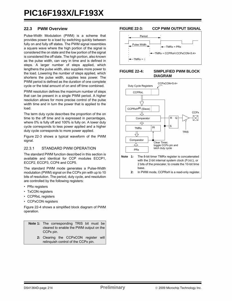
PIC16F193X/LF193X
22.3 PWM Overview
Pulse-Width Modulation (PWM) is a scheme thatprovides power to a load by switching quickly betweenfully on and fully off states. The PWM signal resemblesa square wave where the high portion of the signal isconsidered the on state and the low portion of the signalis considered the off state. The high portion, also knownas the pulse width, can vary in time and is defined insteps. A larger number of steps applied, whichlengthens the pulse width, also supplies more power tothe load. Lowering the number of steps applied, whichshortens the pulse width, supplies less power. ThePWM period is defined as the duration of one completecycle or the total amount of on and off time combined.
PWM resolution defines the maximum number of stepsthat can be present in a single PWM period. A higherresolution allows for more precise control of the pulsewidth time and in turn the power that is applied to theload.
The term duty cycle describes the proportion of the ontime to the off time and is expressed in percentages,where 0% is fully off and 100% is fully on. A lower dutycycle corresponds to less power applied and a higherduty cycle corresponds to more power applied.
Figure 22-3 shows a typical waveform of the PWMsignal.
22.3.1 STANDARD PWM OPERATION
The standard PWM function described in this section isavailable and identical for CCP modules ECCP1,ECCP2, ECCP3, CCP4 and CCP5.
The standard PWM mode generates a Pulse-Widthmodulation (PWM) signal on the CCPx pin with up to 10bits of resolution. The period, duty cycle, and resolutionare controlled by the following registers:
• PRx registers
• TxCON registers
• CCPRxL registers
• CCPxCON registers
Figure 22-4 shows a simplified block diagram of PWMoperation.
FIGURE 22-3: CCP PWM OUTPUT SIGNAL
FIGURE 22-4: SIMPLIFIED PWM BLOCK DIAGRAM
Note 1: The corresponding TRIS bit must becleared to enable the PWM output on theCCPx pin.
2: Clearing the CCPxCON register willrelinquish control of the CCPx pin.
Period
Pulse Width
TMRx = 0
TMRx = CCPRxH:CCPxCON<5:4>
TMRx = PRx
CCPRxL
CCPRxH(2) (Slave)
Comparator
TMRx
PRx
(1)
R Q
S
Duty Cycle RegistersCCPxCON<5:4>
Clear Timer,toggle CCPx pin and latch duty cycle
Note 1: The 8-bit timer TMRx register is concatenated with the 2-bit internal system clock (FOSC), or 2 bits of the prescaler, to create the 10-bit time base.
2: In PWM mode, CCPRxH is a read-only register.
TRIS
CCPx
Comparator
DS41364D-page 214 Preliminary 2009 Microchip Technology Inc.
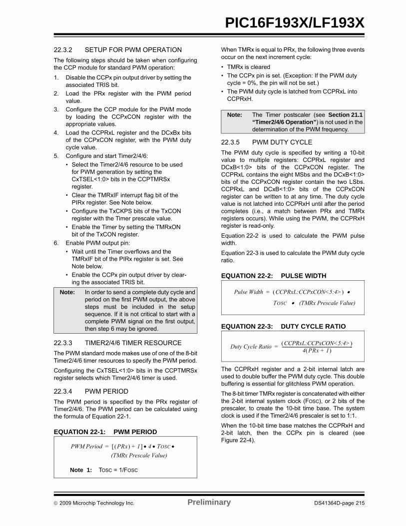
PIC16F193X/LF193X
22.3.2 SETUP FOR PWM OPERATION
The following steps should be taken when configuringthe CCP module for standard PWM operation:
1. Disable the CCPx pin output driver by setting theassociated TRIS bit.
2. Load the PRx register with the PWM periodvalue.
3. Configure the CCP module for the PWM modeby loading the CCPxCON register with theappropriate values.
4. Load the CCPRxL register and the DCxBx bitsof the CCPxCON register, with the PWM dutycycle value.
5. Configure and start Timer2/4/6:
• Select the Timer2/4/6 resource to be used for PWM generation by setting the CxTSEL<1:0> bits in the CCPTMRSx register.
• Clear the TMRxIF interrupt flag bit of the PIRx register. See Note below.
• Configure the TxCKPS bits of the TxCON register with the Timer prescale value.
• Enable the Timer by setting the TMRxON bit of the TxCON register.
6. Enable PWM output pin:
• Wait until the Timer overflows and the TMRxIF bit of the PIRx register is set. See Note below.
• Enable the CCPx pin output driver by clear-ing the associated TRIS bit.
22.3.3 TIMER2/4/6 TIMER RESOURCE
The PWM standard mode makes use of one of the 8-bitTimer2/4/6 timer resources to specify the PWM period.
Configuring the CxTSEL<1:0> bits in the CCPTMRSxregister selects which Timer2/4/6 timer is used.
22.3.4 PWM PERIOD
The PWM period is specified by the PRx register ofTimer2/4/6. The PWM period can be calculated usingthe formula of Equation 22-1.
EQUATION 22-1: PWM PERIOD
When TMRx is equal to PRx, the following three eventsoccur on the next increment cycle:
• TMRx is cleared
• The CCPx pin is set. (Exception: If the PWM duty cycle = 0%, the pin will not be set.)
• The PWM duty cycle is latched from CCPRxL into CCPRxH.
22.3.5 PWM DUTY CYCLE
The PWM duty cycle is specified by writing a 10-bitvalue to multiple registers: CCPRxL register andDCxB<1:0> bits of the CCPxCON register. TheCCPRxL contains the eight MSbs and the DCxB<1:0>bits of the CCPxCON register contain the two LSbs.CCPRxL and DCxB<1:0> bits of the CCPxCONregister can be written to at any time. The duty cyclevalue is not latched into CCPRxH until after the periodcompletes (i.e., a match between PRx and TMRxregisters occurs). While using the PWM, the CCPRxHregister is read-only.
Equation 22-2 is used to calculate the PWM pulsewidth.
Equation 22-3 is used to calculate the PWM duty cycleratio.
EQUATION 22-2: PULSE WIDTH
EQUATION 22-3: DUTY CYCLE RATIO
The CCPRxH register and a 2-bit internal latch areused to double buffer the PWM duty cycle. This doublebuffering is essential for glitchless PWM operation.
The 8-bit timer TMRx register is concatenated with eitherthe 2-bit internal system clock (FOSC), or 2 bits of theprescaler, to create the 10-bit time base. The systemclock is used if the Timer2/4/6 prescaler is set to 1:1.
When the 10-bit time base matches the CCPRxH and2-bit latch, then the CCPx pin is cleared (seeFigure 22-4).
Note: In order to send a complete duty cycle andperiod on the first PWM output, the abovesteps must be included in the setupsequence. If it is not critical to start with acomplete PWM signal on the first output,then step 6 may be ignored.
PWM Period PRx 1+ 4 TOSC =
(TMRx Prescale Value)
Note 1: TOSC = 1/FOSC
Note: The Timer postscaler (see Section 21.1“Timer2/4/6 Operation”) is not used in thedetermination of the PWM frequency.
Pulse Width CCPRxL:CCPxCON<5:4> =
TOSC (TMRx Prescale Value)
Duty Cycle RatioCCPRxL:CCPxCON<5:4>
4 PRx 1+ -----------------------------------------------------------------------=
2009 Microchip Technology Inc. Preliminary DS41364D-page 215

PIC16F193X/LF193X
22.3.6 PWM RESOLUTION
The resolution determines the number of available dutycycles for a given period. For example, a 10-bit resolutionwill result in 1024 discrete duty cycles, whereas an 8-bitresolution will result in 256 discrete duty cycles.
The maximum PWM resolution is 10 bits when PRx is255. The resolution is a function of the PRx registervalue as shown by Equation 22-4.
EQUATION 22-4: PWM RESOLUTION
TABLE 22-4: EXAMPLE PWM FREQUENCIES AND RESOLUTIONS (FOSC = 32 MHz)
TABLE 22-5: EXAMPLE PWM FREQUENCIES AND RESOLUTIONS (FOSC = 20 MHz)
TABLE 22-6: EXAMPLE PWM FREQUENCIES AND RESOLUTIONS (FOSC = 8 MHz)
Note: If the pulse width value is greater than theperiod the assigned PWM pin(s) willremain unchanged.
Resolution4 PRx 1+ log
2 log------------------------------------------ bits=
PWM Frequency 1.95 kHz 7.81 kHz 31.25 kHz 125 kHz 250 kHz 333.3 kHz
Timer Prescale (1, 4, 16) 16 4 1 1 1 1
PRx Value 0xFF 0xFF 0xFF 0x3F 0x1F 0x17
Maximum Resolution (bits) 10 10 10 8 7 6.6
PWM Frequency 1.22 kHz 4.88 kHz 19.53 kHz 78.12 kHz 156.3 kHz 208.3 kHz
Timer Prescale (1, 4, 16) 16 4 1 1 1 1
PRx Value 0xFF 0xFF 0xFF 0x3F 0x1F 0x17
Maximum Resolution (bits) 10 10 10 8 7 6.6
PWM Frequency 1.22 kHz 4.90 kHz 19.61 kHz 76.92 kHz 153.85 kHz 200.0 kHz
Timer Prescale (1, 4, 16) 16 4 1 1 1 1
PRx Value 0x65 0x65 0x65 0x19 0x0C 0x09
Maximum Resolution (bits) 8 8 8 6 5 5
DS41364D-page 216 Preliminary 2009 Microchip Technology Inc.

PIC16F193X/LF193X
22.3.7 OPERATION IN SLEEP MODE
In Sleep mode, the TMRx register will not incrementand the state of the module will not change. If the CCPxpin is driving a value, it will continue to drive that value.When the device wakes up, TMRx will continue from itsprevious state.
22.3.8 CHANGES IN SYSTEM CLOCK FREQUENCY
The PWM frequency is derived from the system clockfrequency. Any changes in the system clock frequencywill result in changes to the PWM frequency. SeeSection 5.0 “Oscillator Module (With Fail-SafeClock Monitor)” for additional details.
22.3.9 EFFECTS OF RESET
Any Reset will force all ports to Input mode and theCCP registers to their Reset states.
TABLE 22-7: SUMMARY OF REGISTERS ASSOCIATED WITH STANDARD PWM
Name Bit 7 Bit 6 Bit 5 Bit 4 Bit 3 Bit 2 Bit 1 Bit 0Register on Page
CCPxCON PxM<1:0>(1) DCxB<1:0> CCPxM<3:0> 231
CCPTMRS0 C4TSEL<1:0> C3TSEL<1:0> C2TSEL<1:0> C1TSEL<1:0> 232
CCPTMRS1 — — — — — — C5TSEL<1:0> 233
INTCON GIE PEIE TMR0IE INTE IOCIE TMR0IF INTF IOCIF 99
PIE1 TMR1GIE ADIE RCIE TXIE SSPIE CCP1IE TMR2IE TMR1IE 100
PIE2 OSFIE C2IE C1IE EEIE BCLIE LCDIE — CCP2IE 101
PIE3 — CCP5IE CCP4IE CCP3IE TMR6IE — TMR4IE — 102
PIR1 TMR1GIF ADIF RCIF TXIF SSPIF CCP1IF TMR2IF TMR1IF 103
PIR2 OSFIF C2IF C1IF EEIF BCLIF LCDIF — CCP2IF 104
PIR3 — CCP5IF CCP4IF CCP3IF TMR6IF — TMR4IF — 105
PRx Timer2/4/6 Period Register 205*
TxCON — TxOUTPS<3:0> TMRxON TxCKPS<:0>1 207
TMRx Timer2/4/6 Module Register 205
TRISA TRISA7 TRISA6 TRISA5 TRISA4 TRISA3 TRISA2 TRISA1 TRISA0 132
TRISB TRISB7 TRISB6 TRISB5 TRISB4 TRISB3 TRISB2 TRISB1 TRISB0 137
TRISC TRISC7 TRISC6 TRISC5 TRISC4 TRISC3 TRISC2 TRISC1 TRISC0 140
TRISD(2) TRISD7 TRISD6 TRISD5 TRISD4 TRISD3 TRISD2 TRISD1 TRISD0 143
TRISE — — — — TRISE3 TRISE2(2) TRISE1(2) TRISE0(2) 146
Legend: — = Unimplemented location, read as ‘0’. Shaded cells are not used by the PWM.Note 1: Applies to ECCP modules only.
2: These registers/bits are not implemented on PIC16F1933/1936/1938/PIC16LF1933/1936/1938 devices, read as ‘0’.* Page provides register information.
2009 Microchip Technology Inc. Preliminary DS41364D-page 217

PIC16F193X/LF193X
22.4 PWM (Enhanced Mode)
The enhanced PWM function described in this section isavailable for CCP modules ECCP1, ECCP2 andECCP3, with any differences between modules noted.
The enhanced PWM mode generates a Pulse-WidthModulation (PWM) signal on up to four different outputpins with up to 10 bits of resolution. The period, dutycycle, and resolution are controlled by the followingregisters:
• PRx registers
• TxCON registers
• CCPRxL registers
• CCPxCON registers
The ECCP modules have the following additional PWMregisters which control Auto-shutdown, Auto-restart,Dead-band Delay and PWM Steering modes:
• CCPxAS registers
• PSTRxCON registers
• PWMxCON registers
The enhanced PWM module can generate the followingfive PWM Output modes:
• Single PWM
• Half-Bridge PWM
• Full-Bridge PWM, Forward Mode
• Full-Bridge PWM, Reverse Mode
• Single PWM with PWM Steering Mode
To select an Enhanced PWM Output mode, the PxM bitsof the CCPxCON register must be configuredappropriately.
The PWM outputs are multiplexed with I/O pins and aredesignated PxA, PxB, PxC and PxD. The polarity of thePWM pins is configurable and is selected by setting theCCPxM bits in the CCPxCON register appropriately.
Figure 22-5 shows an example of a simplified blockdiagram of the Enhanced PWM module.
Table 22-8 shows the pin assignments for variousEnhanced PWM modes.
FIGURE 22-5: EXAMPLE SIMPLIFIED BLOCK DIAGRAM OF THE ENHANCED PWM MODE
Note 1: The corresponding TRIS bit must becleared to enable the PWM output on theCCPx pin.
2: Clearing the CCPxCON register willrelinquish control of the CCPx pin.
3: Any pin not used in the enhanced PWMmode is available for alternate pinfunctions, if applicable.
4: To prevent the generation of anincomplete waveform when the PWM isfirst enabled, the ECCP module waitsuntil the start of a new PWM period beforegenerating a PWM signal.
CCPRxL
CCPRxH (Slave)
Comparator
TMRx
Comparator
PRx
(1)
R Q
S
Duty Cycle RegistersDCxB<1:0>
Clear Timer,toggle PWM pin and latch duty cycle
Note 1: The 8-bit timer TMRx register is concatenated with the 2-bit internal Q clock, or 2 bits of the prescaler to create the 10-bit timebase.
TRISx
CCPx/PxA
TRISx
PxB
TRISx
PxC
TRISx
PxD
OutputController
PxM<1:0>2
CCPxM<3:0>4
PWMxCON
CCPx/PxA
PxB
PxC
PxD
DS41364D-page 218 Preliminary 2009 Microchip Technology Inc.
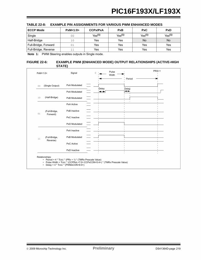
PIC16F193X/LF193X
TABLE 22-8: EXAMPLE PIN ASSIGNMENTS FOR VARIOUS PWM ENHANCED MODES
FIGURE 22-6: EXAMPLE PWM (ENHANCED MODE) OUTPUT RELATIONSHIPS (ACTIVE-HIGH STATE)
ECCP Mode PxM<1:0> CCPx/PxA PxB PxC PxD
Single 00 Yes(1) Yes(1) Yes(1) Yes(1)
Half-Bridge 10 Yes Yes No No
Full-Bridge, Forward 01 Yes Yes Yes Yes
Full-Bridge, Reverse 11 Yes Yes Yes Yes
Note 1: PWM Steering enables outputs in Single mode.
0
Period
00
10
01
11
SignalPRX+1
PxM<1:0>
PxA Modulated
PxA Modulated
PxB Modulated
PxA Active
PxB Inactive
PxC Inactive
PxD Modulated
PxA Inactive
PxB Modulated
PxC Active
PxD Inactive
PulseWidth
(Single Output)
(Half-Bridge)
(Full-Bridge,Forward)
(Full-Bridge,Reverse)
Delay Delay
Relationships:• Period = 4 * TOSC * (PRx + 1) * (TMRx Prescale Value)• Pulse Width = TOSC * (CCPRxL<7:0>:CCPxCON<5:4>) * (TMRx Prescale Value)• Delay = 4 * TOSC * (PWMxCON<6:0>)
2009 Microchip Technology Inc. Preliminary DS41364D-page 219

PIC16F193X/LF193X
FIGURE 22-7: EXAMPLE ENHANCED PWM OUTPUT RELATIONSHIPS (ACTIVE-LOW STATE)
0
Period
00
10
01
11
SignalPRx+1
PxM<1:0>
PxA Modulated
PxA Modulated
PxB Modulated
PxA Active
PxB Inactive
PxC Inactive
PxD Modulated
PxA Inactive
PxB Modulated
PxC Active
PxD Inactive
Pulse
Width
(Single Output)
(Half-Bridge)
(Full-Bridge,
Forward)
(Full-Bridge,
Reverse)
Delay Delay
Relationships:• Period = 4 * TOSC * (PRx + 1) * (TMRx Prescale Value)• Pulse Width = TOSC * (CCPRxL<7:0>:CCPxCON<5:4>) * (TMRx Prescale Value)• Delay = 4 * TOSC * (PWMxCON<6:0>)
DS41364D-page 220 Preliminary 2009 Microchip Technology Inc.

PIC16F193X/LF193X
22.4.1 HALF-BRIDGE MODE
In Half-Bridge mode, two pins are used as outputs todrive push-pull loads. The PWM output signal is outputon the CCPx/PxA pin, while the complementary PWMoutput signal is output on the PxB pin (seeFigure 22-9). This mode can be used for Half-Bridgeapplications, as shown in Figure 22-9, or for Full-Bridgeapplications, where four power switches are beingmodulated with two PWM signals.
In Half-Bridge mode, the programmable dead-band delaycan be used to prevent shoot-through current inHalf-Bridge power devices. The value of the PDC<6:0>bits of the PWMxCON register sets the number ofinstruction cycles before the output is driven active. If thevalue is greater than the duty cycle, the correspondingoutput remains inactive during the entire cycle. SeeSection 22.4.5 “Programmable Dead-Band DelayMode” for more details of the dead-band delayoperations.
Since the PxA and PxB outputs are multiplexed with thePORT data latches, the associated TRIS bits must becleared to configure PxA and PxB as outputs.
FIGURE 22-8: EXAMPLE OF HALF-BRIDGE PWM OUTPUT
FIGURE 22-9: EXAMPLE OF HALF-BRIDGE APPLICATIONS
Period
Pulse Width
td
td
(1)
PxA(2)
PxB(2)
td = Dead-Band Delay
Period
(1) (1)
Note 1: At this time, the TMRx register is equal to thePRx register.
2: Output signals are shown as active-high.
PxA
PxB
FETDriver
FETDriver
Load
+
-
+
-
FETDriver
FETDriver
V+
Load
FETDriver
FETDriver
PxA
PxB
Standard Half-Bridge Circuit (“Push-Pull”)
Half-Bridge Output Driving a Full-Bridge Circuit
2009 Microchip Technology Inc. Preliminary DS41364D-page 221

PIC16F193X/LF193X
22.4.2 FULL-BRIDGE MODE
In Full-Bridge mode, all four pins are used as outputs.An example of Full-Bridge application is shown inFigure 22-10.
In the Forward mode, pin CCPx/PxA is driven to its activestate, pin PxD is modulated, while PxB and PxC will bedriven to their inactive state as shown in Figure 22-11.
In the Reverse mode, PxC is driven to its active state, pinPxB is modulated, while PxA and PxD will be driven totheir inactive state as shown Figure 22-11.
PxA, PxB, PxC and PxD outputs are multiplexed withthe PORT data latches. The associated TRIS bits mustbe cleared to configure the PxA, PxB, PxC and PxDpins as outputs.
FIGURE 22-10: EXAMPLE OF FULL-BRIDGE APPLICATION
PxA
PxC
FETDriver
FETDriver
V+
V-
Load
FETDriver
FETDriver
PxB
PxD
QA
QB QD
QC
DS41364D-page 222 Preliminary 2009 Microchip Technology Inc.
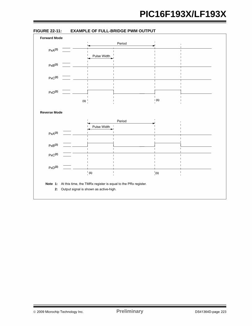
PIC16F193X/LF193X
FIGURE 22-11: EXAMPLE OF FULL-BRIDGE PWM OUTPUT
Period
Pulse Width
PxA(2)
PxB(2)
PxC(2)
PxD(2)
Forward Mode
(1)
Period
Pulse Width
PxA(2)
PxC(2)
PxD(2)
PxB(2)
Reverse Mode
(1)
(1)(1)
Note 1: At this time, the TMRx register is equal to the PRx register.
2: Output signal is shown as active-high.
2009 Microchip Technology Inc. Preliminary DS41364D-page 223

PIC16F193X/LF193X
22.4.2.1 Direction Change in Full-Bridge Mode
In the Full-Bridge mode, the PxM1 bit in the CCPxCONregister allows users to control the forward/reversedirection. When the application firmware changes thisdirection control bit, the module will change to the newdirection on the next PWM cycle.
A direction change is initiated in software by changingthe PxM1 bit of the CCPxCON register. The followingsequence occurs four Timer cycles prior to the end ofthe current PWM period:
• The modulated outputs (PxB and PxD) are placed in their inactive state.
• The associated unmodulated outputs (PxA and PxC) are switched to drive in the opposite direction.
• PWM modulation resumes at the beginning of the next period.
See Figure 22-12 for an illustration of this sequence.
The Full-Bridge mode does not provide dead-banddelay. As one output is modulated at a time, dead-banddelay is generally not required. There is a situationwhere dead-band delay is required. This situationoccurs when both of the following conditions are true:
1. The direction of the PWM output changes whenthe duty cycle of the output is at or near 100%.
2. The turn off time of the power switch, includingthe power device and driver circuit, is greaterthan the turn on time.
Figure 22-13 shows an example of the PWM directionchanging from forward to reverse, at a near 100% dutycycle. In this example, at time t1, the output PxA andPxD become inactive, while output PxC becomesactive. Since the turn off time of the power devices islonger than the turn on time, a shoot-through currentwill flow through power devices QC and QD (seeFigure 22-10) for the duration of ‘t’. The samephenomenon will occur to power devices QA and QBfor PWM direction change from reverse to forward.
If changing PWM direction at high duty cycle is requiredfor an application, two possible solutions for eliminatingthe shoot-through current are:
1. Reduce PWM duty cycle for one PWM periodbefore changing directions.
2. Use switch drivers that can drive the switches offfaster than they can drive them on.
Other options to prevent shoot-through current mayexist.
FIGURE 22-12: EXAMPLE OF PWM DIRECTION CHANGE
Pulse Width
Period(1)Signal
Note 1: The direction bit PxM1 of the CCPxCON register is written any time during the PWM cycle.
2: When changing directions, the PxA and PxC signals switch before the end of the current PWM cycle. Themodulated PxB and PxD signals are inactive at this time. The length of this time is four Timer counts.
Period
(2)
PxA (Active-High)
PxB (Active-High)
PxC (Active-High)
PxD (Active-High)
Pulse Width
DS41364D-page 224 Preliminary 2009 Microchip Technology Inc.
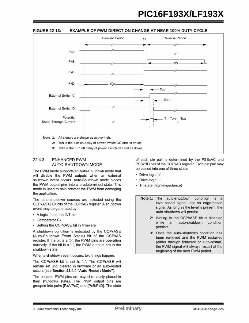
PIC16F193X/LF193X
FIGURE 22-13: EXAMPLE OF PWM DIRECTION CHANGE AT NEAR 100% DUTY CYCLE
22.4.3 ENHANCED PWM AUTO-SHUTDOWN MODE
The PWM mode supports an Auto-Shutdown mode thatwill disable the PWM outputs when an externalshutdown event occurs. Auto-Shutdown mode placesthe PWM output pins into a predetermined state. Thismode is used to help prevent the PWM from damagingthe application.
The auto-shutdown sources are selected using theCCPxAS<2:0> bits of the CCPxAS register. A shutdownevent may be generated by:
• A logic ‘0’ on the INT pin
• Comparator Cx
• Setting the CCPxASE bit in firmware
A shutdown condition is indicated by the CCPxASE(Auto-Shutdown Event Status) bit of the CCPxASregister. If the bit is a ‘0’, the PWM pins are operatingnormally. If the bit is a ‘1’, the PWM outputs are in theshutdown state.
When a shutdown event occurs, two things happen:
The CCPxASE bit is set to ‘1’. The CCPxASE willremain set until cleared in firmware or an auto-restartoccurs (see Section 22.4.4 “Auto-Restart Mode”).
The enabled PWM pins are asynchronously placed intheir shutdown states. The PWM output pins aregrouped into pairs [PxA/PxC] and [PxB/PxD]. The state
of each pin pair is determined by the PSSxAC andPSSxBD bits of the CCPxAS register. Each pin pair maybe placed into one of three states:
• Drive logic ‘1’
• Drive logic ‘0’
• Tri-state (high-impedance)
Forward Period Reverse Period
PxA
TON
TOFF
T = TOFF – TON
PxB
PxC
PxD
External Switch D
PotentialShoot-Through Current
Note 1: All signals are shown as active-high.
2: TON is the turn on delay of power switch QC and its driver.
3: TOFF is the turn off delay of power switch QD and its driver.
External Switch C
t1
PW
PW
Note 1: The auto-shutdown condition is alevel-based signal, not an edge-basedsignal. As long as the level is present, theauto-shutdown will persist.
2: Writing to the CCPxASE bit is disabledwhile an auto-shutdown conditionpersists.
3: Once the auto-shutdown condition hasbeen removed and the PWM restarted(either through firmware or auto-restart)the PWM signal will always restart at thebeginning of the next PWM period.
2009 Microchip Technology Inc. Preliminary DS41364D-page 225
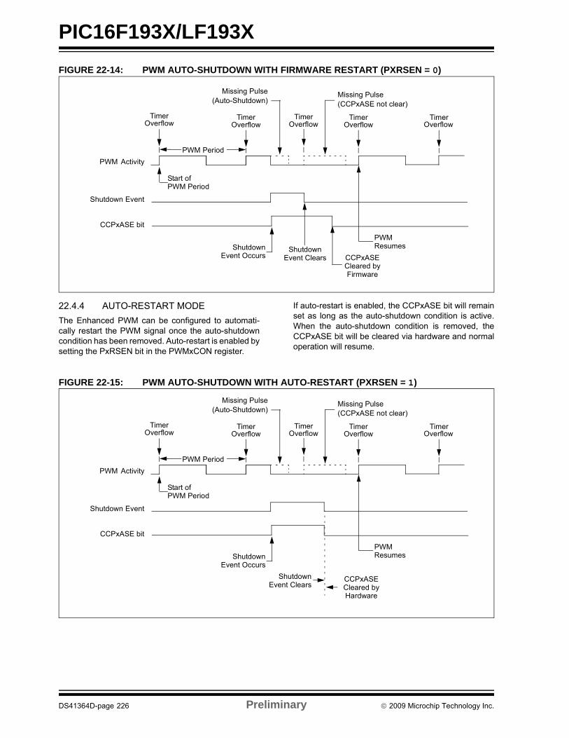
PIC16F193X/LF193X
FIGURE 22-14: PWM AUTO-SHUTDOWN WITH FIRMWARE RESTART (PXRSEN = 0)
22.4.4 AUTO-RESTART MODE
The Enhanced PWM can be configured to automati-cally restart the PWM signal once the auto-shutdowncondition has been removed. Auto-restart is enabled bysetting the PxRSEN bit in the PWMxCON register.
If auto-restart is enabled, the CCPxASE bit will remainset as long as the auto-shutdown condition is active.When the auto-shutdown condition is removed, theCCPxASE bit will be cleared via hardware and normaloperation will resume.
FIGURE 22-15: PWM AUTO-SHUTDOWN WITH AUTO-RESTART (PXRSEN = 1)
Shutdown
PWM
CCPxASE bit
Activity
Event
ShutdownEvent Occurs
ShutdownEvent Clears
PWMResumes
PWM Period
Start ofPWM Period
CCPxASECleared byFirmware
TimerOverflow
TimerOverflow
TimerOverflow
TimerOverflow
Missing Pulse(Auto-Shutdown)
Missing Pulse(CCPxASE not clear)
TimerOverflow
Shutdown
PWM
CCPxASE bit
Activity
Event
ShutdownEvent Occurs
ShutdownEvent Clears
PWM Period
Start ofPWM Period
CCPxASECleared byHardware
TimerOverflow
TimerOverflow
TimerOverflow
TimerOverflow
Missing Pulse(Auto-Shutdown)
Missing Pulse(CCPxASE not clear)
TimerOverflow
PWMResumes
DS41364D-page 226 Preliminary 2009 Microchip Technology Inc.

PIC16F193X/LF193X
22.4.5 PROGRAMMABLE DEAD-BAND DELAY MODE
In Half-Bridge applications where all power switchesare modulated at the PWM frequency, the powerswitches normally require more time to turn off than toturn on. If both the upper and lower power switches areswitched at the same time (one turned on, and theother turned off), both switches may be on for a shortperiod of time until one switch completely turns off.During this brief interval, a very high current(shoot-through current) will flow through both powerswitches, shorting the bridge supply. To avoid thispotentially destructive shoot-through current fromflowing during switching, turning on either of the powerswitches is normally delayed to allow the other switchto completely turn off.
In Half-Bridge mode, a digitally programmabledead-band delay is available to avoid shoot-throughcurrent from destroying the bridge power switches. Thedelay occurs at the signal transition from the non-activestate to the active state. See Figure 22-16 forillustration. The lower seven bits of the associatedPWMxCON register (Register 22-5) sets the delayperiod in terms of microcontroller instruction cycles(TCY or 4 TOSC).
FIGURE 22-16: EXAMPLE OF HALF-BRIDGE PWM OUTPUT
FIGURE 22-17: EXAMPLE OF HALF-BRIDGE APPLICATIONS
Period
Pulse Width
td
td
(1)
PxA(2)
PxB(2)
td = Dead-Band Delay
Period
(1) (1)
Note 1: At this time, the TMRx register is equal to thePRx register.
2: Output signals are shown as active-high.
PxA
PxB
FETDriver
FETDriver
V+
V-
Load
+V-
+V-
Standard Half-Bridge Circuit (“Push-Pull”)
2009 Microchip Technology Inc. Preliminary DS41364D-page 227
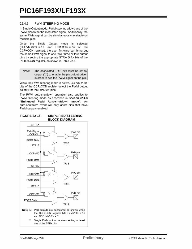
PIC16F193X/LF193X
22.4.6 PWM STEERING MODE
In Single Output mode, PWM steering allows any of thePWM pins to be the modulated signal. Additionally, thesame PWM signal can be simultaneously available onmultiple pins.
Once the Single Output mode is selected(CCPxM<3:2> = 11 and PxM<1:0> = 00 of theCCPxCON register), the user firmware can bring outthe same PWM signal to one, two, three or four outputpins by setting the appropriate STRx<D:A> bits of thePSTRxCON register, as shown in Table 22-8.
While the PWM Steering mode is active, CCPxM<1:0>bits of the CCPxCON register select the PWM outputpolarity for the Px<D:A> pins.
The PWM auto-shutdown operation also applies toPWM Steering mode as described in Section 22.4.3“Enhanced PWM Auto-shutdown mode”. Anauto-shutdown event will only affect pins that havePWM outputs enabled.
FIGURE 22-18: SIMPLIFIED STEERING BLOCK DIAGRAM
Note: The associated TRIS bits must be set tooutput (‘0’) to enable the pin output driverin order to see the PWM signal on the pin.
1
0TRIS
PxA pin
PORT Data
PxA Signal
STRxA
1
0TRIS
PxB pin
PORT Data
STRxB
1
0TRIS
PxC pin
PORT Data
STRxC
1
0TRIS
PxD pin
PORT Data
STRxD
Note 1: Port outputs are configured as shown whenthe CCPxCON register bits PxM<1:0> = 00and CCPxM<3:2> = 11.
2: Single PWM output requires setting at leastone of the STRx bits.
CCPxM1
CCPxM0
CCPxM1
CCPxM0
DS41364D-page 228 Preliminary 2009 Microchip Technology Inc.
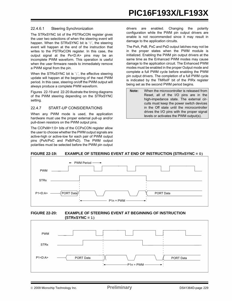
PIC16F193X/LF193X
22.4.6.1 Steering Synchronization
The STRxSYNC bit of the PSTRxCON register givesthe user two selections of when the steering event willhappen. When the STRxSYNC bit is ‘0’, the steeringevent will happen at the end of the instruction thatwrites to the PSTRxCON register. In this case, theoutput signal at the Px<D:A> pins may be anincomplete PWM waveform. This operation is usefulwhen the user firmware needs to immediately removea PWM signal from the pin.
When the STRxSYNC bit is ‘1’, the effective steeringupdate will happen at the beginning of the next PWMperiod. In this case, steering on/off the PWM output willalways produce a complete PWM waveform.
Figures 22-19 and 22-20 illustrate the timing diagramsof the PWM steering depending on the STRxSYNCsetting.
22.4.7 START-UP CONSIDERATIONS
When any PWM mode is used, the applicationhardware must use the proper external pull-up and/orpull-down resistors on the PWM output pins.
The CCPxM<1:0> bits of the CCPxCON register allowthe user to choose whether the PWM output signals areactive-high or active-low for each pair of PWM outputpins (PxA/PxC and PxB/PxD). The PWM outputpolarities must be selected before the PWM pin output
drivers are enabled. Changing the polarityconfiguration while the PWM pin output drivers areenable is not recommended since it may result indamage to the application circuits.
The PxA, PxB, PxC and PxD output latches may not bein the proper states when the PWM module isinitialized. Enabling the PWM pin output drivers at thesame time as the Enhanced PWM modes may causedamage to the application circuit. The Enhanced PWMmodes must be enabled in the proper Output mode andcomplete a full PWM cycle before enabling the PWMpin output drivers. The completion of a full PWM cycleis indicated by the TMRxIF bit of the PIRx registerbeing set as the second PWM period begins.
FIGURE 22-19: EXAMPLE OF STEERING EVENT AT END OF INSTRUCTION (STRxSYNC = 0)
FIGURE 22-20: EXAMPLE OF STEERING EVENT AT BEGINNING OF INSTRUCTION(STRxSYNC = 1)
Note: When the microcontroller is released fromReset, all of the I/O pins are in thehigh-impedance state. The external cir-cuits must keep the power switch devicesin the Off state until the microcontrollerdrives the I/O pins with the proper signallevels or activates the PWM output(s).
PWM
P1n = PWM
STRx
P1<D:A> PORT Data
PWM Period
PORT Data
PWM
PORT Data
P1n = PWM
STRx
P1<D:A> PORT Data
2009 Microchip Technology Inc. Preliminary DS41364D-page 229

PIC16F193X/LF193X
TABLE 22-9: SUMMARY OF REGISTERS ASSOCIATED WITH ENHANCED PWM
Name Bit 7 Bit 6 Bit 5 Bit 4 Bit 3 Bit 2 Bit 1 Bit 0Register on Page
CCPxCON PxM<1:0>(1) DCxB<1:0> CCPxM<3:0> 231
CCPxAS CCPxASE CCPxAS<2:0> PSSxAC<1:0> PSSxBD<1:0> 234
CCPTMRS0 C4TSEL<1:0> C3TSEL<1:0> C2TSEL<1:0> C1TSEL<1:0> 232
CCPTMRS1 — — — — — — C5TSEL<1:0> 233
INTCON GIE PEIE TMR0IE INTE IOCIE TMR0IF INTF IOCIF 99
PIE1 TMR1GIE ADIE RCIE TXIE SSPIE CCP1IE TMR2IE TMR1IE 100
PIE2 OSFIE C2IE C1IE EEIE BCLIE LCDIE — CCP2IE 101
PIE3 — CCP5IE CCP4IE CCP3IE TMR6IE — TMR4IE — 102
PIR1 TMR1GIF ADIF RCIF TXIF SSPIF CCP1IF TMR2IF TMR1IF 103
PIR2 OSFIF C2IF C1IF EEIF BCLIF LCDIF — CCP2IF 104
PIR3 — CCP5IF CCP4IF CCP3IF TMR6IF — TMR4IF — 105
PRx Timer2/4/6 Period Register 205*
PSTRxCON — — — STRxSYNC STRxD STRxC STRxB STRxA 236
PWMxCON PxRSEN PxDC<6:0> 235
TxCON — TxOUTPS<3:0> TMRxON TxCKPS<:0>1 207
TMRx Timer2/4/6 Module Register 205
TRISA TRISA7 TRISA6 TRISA5 TRISA4 TRISA3 TRISA2 TRISA1 TRISA0 216
TRISB TRISB7 TRISB6 TRISB5 TRISB4 TRISB3 TRISB2 TRISB1 TRISB0 216
TRISC TRISC7 TRISC6 TRISC5 TRISC4 TRISC3 TRISC2 TRISC1 TRISC0 216
TRISD(2) TRISD7 TRISD6 TRISD5 TRISD4 TRISD3 TRISD2 TRISD1 TRISD0 216
TRISE — — — — TRISE3 TRISE2(2) TRISE1(2) TRISE0(2) 216
Legend: — = Unimplemented location, read as ‘0’. Shaded cells are not used by the PWM.Note 1: Applies to ECCP modules only.
2: These registers/bits are not implemented on PIC16F1933/1936/1938/PIC16LF1933/1936/1938 devices, read as ‘0’.* Page provides register information.
DS41364D-page 230 Preliminary 2009 Microchip Technology Inc.
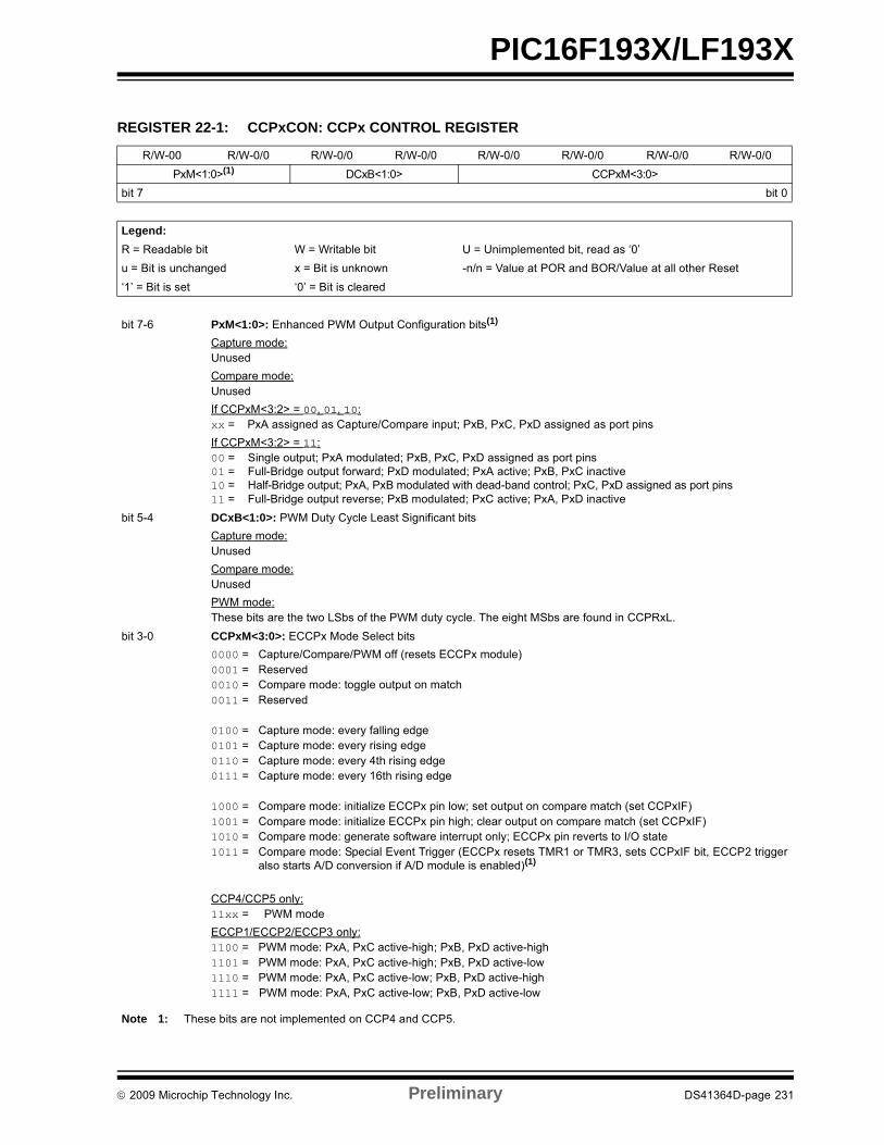
PIC16F193X/LF193X
REGISTER 22-1: CCPxCON: CCPx CONTROL REGISTER
R/W-00 R/W-0/0 R/W-0/0 R/W-0/0 R/W-0/0 R/W-0/0 R/W-0/0 R/W-0/0
PxM<1:0>(1) DCxB<1:0> CCPxM<3:0>
bit 7 bit 0
Legend:
R = Readable bit W = Writable bit U = Unimplemented bit, read as ‘0’
u = Bit is unchanged x = Bit is unknown -n/n = Value at POR and BOR/Value at all other Reset
‘1’ = Bit is set ‘0’ = Bit is cleared
bit 7-6 PxM<1:0>: Enhanced PWM Output Configuration bits(1)
Capture mode:Unused
Compare mode:Unused
If CCPxM<3:2> = 00, 01, 10:xx = PxA assigned as Capture/Compare input; PxB, PxC, PxD assigned as port pins
If CCPxM<3:2> = 11:00 = Single output; PxA modulated; PxB, PxC, PxD assigned as port pins01 = Full-Bridge output forward; PxD modulated; PxA active; PxB, PxC inactive10 = Half-Bridge output; PxA, PxB modulated with dead-band control; PxC, PxD assigned as port pins11 = Full-Bridge output reverse; PxB modulated; PxC active; PxA, PxD inactive
bit 5-4 DCxB<1:0>: PWM Duty Cycle Least Significant bits
Capture mode:Unused
Compare mode:Unused
PWM mode:These bits are the two LSbs of the PWM duty cycle. The eight MSbs are found in CCPRxL.
bit 3-0 CCPxM<3:0>: ECCPx Mode Select bits
0000 = Capture/Compare/PWM off (resets ECCPx module)0001 = Reserved 0010 = Compare mode: toggle output on match0011 = Reserved
0100 = Capture mode: every falling edge 0101 = Capture mode: every rising edge0110 = Capture mode: every 4th rising edge 0111 = Capture mode: every 16th rising edge
1000 = Compare mode: initialize ECCPx pin low; set output on compare match (set CCPxIF)1001 = Compare mode: initialize ECCPx pin high; clear output on compare match (set CCPxIF)1010 = Compare mode: generate software interrupt only; ECCPx pin reverts to I/O state1011 = Compare mode: Special Event Trigger (ECCPx resets TMR1 or TMR3, sets CCPxIF bit, ECCP2 trigger
also starts A/D conversion if A/D module is enabled)(1)
CCP4/CCP5 only:11xx = PWM mode
ECCP1/ECCP2/ECCP3 only:1100 = PWM mode: PxA, PxC active-high; PxB, PxD active-high1101 = PWM mode: PxA, PxC active-high; PxB, PxD active-low1110 = PWM mode: PxA, PxC active-low; PxB, PxD active-high1111 = PWM mode: PxA, PxC active-low; PxB, PxD active-low
Note 1: These bits are not implemented on CCP4 and CCP5.
2009 Microchip Technology Inc. Preliminary DS41364D-page 231
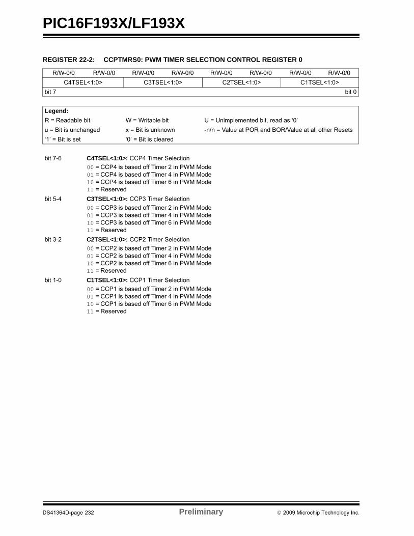
PIC16F193X/LF193X
REGISTER 22-2: CCPTMRS0: PWM TIMER SELECTION CONTROL REGISTER 0
R/W-0/0 R/W-0/0 R/W-0/0 R/W-0/0 R/W-0/0 R/W-0/0 R/W-0/0 R/W-0/0
C4TSEL<1:0> C3TSEL<1:0> C2TSEL<1:0> C1TSEL<1:0>
bit 7 bit 0
Legend:
R = Readable bit W = Writable bit U = Unimplemented bit, read as ‘0’
u = Bit is unchanged x = Bit is unknown -n/n = Value at POR and BOR/Value at all other Resets
‘1’ = Bit is set ‘0’ = Bit is cleared
bit 7-6 C4TSEL<1:0>: CCP4 Timer Selection
00 = CCP4 is based off Timer 2 in PWM Mode01 = CCP4 is based off Timer 4 in PWM Mode10 = CCP4 is based off Timer 6 in PWM Mode11 = Reserved
bit 5-4 C3TSEL<1:0>: CCP3 Timer Selection
00 = CCP3 is based off Timer 2 in PWM Mode01 = CCP3 is based off Timer 4 in PWM Mode10 = CCP3 is based off Timer 6 in PWM Mode11 = Reserved
bit 3-2 C2TSEL<1:0>: CCP2 Timer Selection
00 = CCP2 is based off Timer 2 in PWM Mode01 = CCP2 is based off Timer 4 in PWM Mode10 = CCP2 is based off Timer 6 in PWM Mode11 = Reserved
bit 1-0 C1TSEL<1:0>: CCP1 Timer Selection
00 = CCP1 is based off Timer 2 in PWM Mode01 = CCP1 is based off Timer 4 in PWM Mode10 = CCP1 is based off Timer 6 in PWM Mode11 = Reserved
DS41364D-page 232 Preliminary 2009 Microchip Technology Inc.
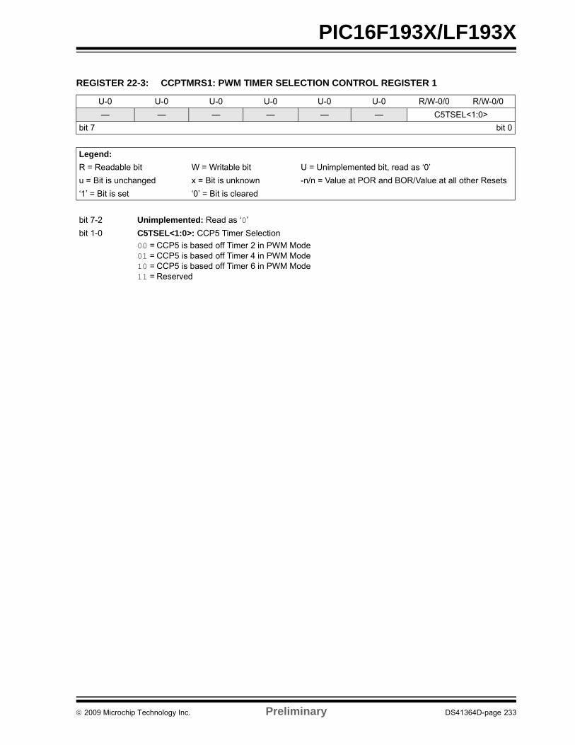
PIC16F193X/LF193X
REGISTER 22-3: CCPTMRS1: PWM TIMER SELECTION CONTROL REGISTER 1
U-0 U-0 U-0 U-0 U-0 U-0 R/W-0/0 R/W-0/0
— — — — — — C5TSEL<1:0>
bit 7 bit 0
Legend:
R = Readable bit W = Writable bit U = Unimplemented bit, read as ‘0’
u = Bit is unchanged x = Bit is unknown -n/n = Value at POR and BOR/Value at all other Resets
‘1’ = Bit is set ‘0’ = Bit is cleared
bit 7-2 Unimplemented: Read as ‘0’
bit 1-0 C5TSEL<1:0>: CCP5 Timer Selection
00 = CCP5 is based off Timer 2 in PWM Mode01 = CCP5 is based off Timer 4 in PWM Mode10 = CCP5 is based off Timer 6 in PWM Mode11 = Reserved
2009 Microchip Technology Inc. Preliminary DS41364D-page 233

PIC16F193X/LF193X
REGISTER 22-4: CCPxAS: CCPX AUTO-SHUTDOWN CONTROL REGISTER
R/W-0/0 R/W-0/0 R/W-0/0 R/W-0/0 R/W-0/0 R/W-0/0 R/W-0/0 R/W-0/0
CCPxASE CCPxAS<2:0> PSSxAC<1:0> PSSxBD<1:0>
bit 7 bit 0
Legend:
R = Readable bit W = Writable bit U = Unimplemented bit, read as ‘0’
u = Bit is unchanged x = Bit is unknown -n/n = Value at POR and BOR/Value at all other Resets
‘1’ = Bit is set ‘0’ = Bit is cleared
bit 7 CCPxASE: CCPx Auto-Shutdown Event Status bit
1 = A shutdown event has occurred; CCPx outputs are in shutdown state0 = CCPx outputs are operating
bit 6-4 CCxPAS<2:0>: CCPx Auto-Shutdown Source Select bits
000 = Auto-shutdown is disabled001 = Comparator C1 output low(1)
010 = Comparator C2 output low(1)
011 = Either Comparator C1 or C2 low(1)
100 = VIL on INT pin101 = VIL on INT pin or Comparator C1 low(1)
110 = VIL on INT pin or Comparator C2 low(1)
111 = VIL on INT pin or Comparator C1 or Comparator C2 low(1)
bit 3-2 PSSxAC<1:0>: Pins PxA and PxC Shutdown State Control bits
00 = Drive pins PxA and PxC to ‘0’01 = Drive pins PxA and PxC to ‘1’1x = Pins PxA and PxC tri-state
bit 1-0 PSSxBD<1:0>: Pins PxB and PxD Shutdown State Control bits
00 = Drive pins PxB and PxD to ‘0’01 = Drive pins PxB and PxD to ‘1’1x = Pins PxB and PxD tri-state
Note 1: If CxSYNC is enabled, the shutdown will be delayed by Timer1.
DS41364D-page 234 Preliminary 2009 Microchip Technology Inc.
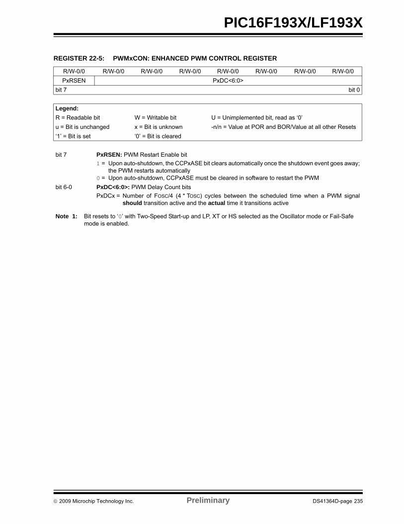
PIC16F193X/LF193X
REGISTER 22-5: PWMxCON: ENHANCED PWM CONTROL REGISTER
R/W-0/0 R/W-0/0 R/W-0/0 R/W-0/0 R/W-0/0 R/W-0/0 R/W-0/0 R/W-0/0
PxRSEN PxDC<6:0>
bit 7 bit 0
Legend:
R = Readable bit W = Writable bit U = Unimplemented bit, read as ‘0’
u = Bit is unchanged x = Bit is unknown -n/n = Value at POR and BOR/Value at all other Resets
‘1’ = Bit is set ‘0’ = Bit is cleared
bit 7 PxRSEN: PWM Restart Enable bit
1 = Upon auto-shutdown, the CCPxASE bit clears automatically once the shutdown event goes away;the PWM restarts automatically
0 = Upon auto-shutdown, CCPxASE must be cleared in software to restart the PWM
bit 6-0 PxDC<6:0>: PWM Delay Count bits
PxDCx = Number of FOSC/4 (4 * TOSC) cycles between the scheduled time when a PWM signalshould transition active and the actual time it transitions active
Note 1: Bit resets to ‘0’ with Two-Speed Start-up and LP, XT or HS selected as the Oscillator mode or Fail-Safe mode is enabled.
2009 Microchip Technology Inc. Preliminary DS41364D-page 235

PIC16F193X/LF193X
REGISTER 22-6: PSTRxCON: PWM STEERING CONTROL REGISTER(1)
U-0 U-0 U-0 R/W-0/0 R/W-0/0 R/W-0/0 R/W-0/0 R/W-1/1
— — — STRxSYNC STRxD STRxC STRxB STRxA
bit 7 bit 0
Legend:
R = Readable bit W = Writable bit U = Unimplemented bit, read as ‘0’
u = Bit is unchanged x = Bit is unknown -n/n = Value at POR and BOR/Value at all other Resets
‘1’ = Bit is set ‘0’ = Bit is cleared
bit 7-5 Unimplemented: Read as ‘0’
bit 4 STRxSYNC: Steering Sync bit
1 = Output steering update occurs on next PWM period0 = Output steering update occurs at the beginning of the instruction cycle boundary
bit 3 STRxD: Steering Enable bit D
1 = PxD pin has the PWM waveform with polarity control from CCPxM<1:0>
0 = PxD pin is assigned to port pin
bit 2 STRxC: Steering Enable bit C
1 = PxC pin has the PWM waveform with polarity control from CCPxM<1:0>
0 = PxC pin is assigned to port pin
bit 1 STRxB: Steering Enable bit B
1 = PxB pin has the PWM waveform with polarity control from CCPxM<1:0>
0 = PxB pin is assigned to port pin
bit 0 STRxA: Steering Enable bit A
1 = PxA pin has the PWM waveform with polarity control from CCPxM<1:0>
0 = PxA pin is assigned to port pin
Note 1: The PWM Steering mode is available only when the CCPxCON register bits CCPxM<3:2> = 11 and PxM<1:0> = 00.
DS41364D-page 236 Preliminary 2009 Microchip Technology Inc.
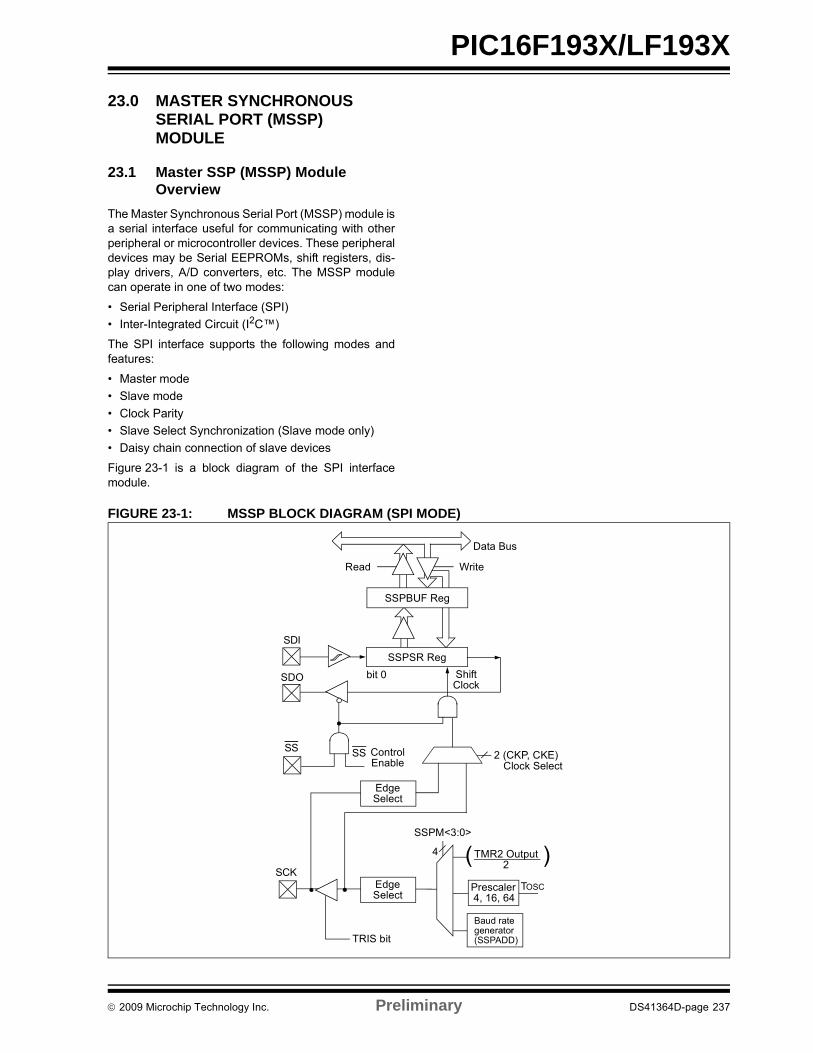
PIC16F193X/LF193X
23.0 MASTER SYNCHRONOUS SERIAL PORT (MSSP) MODULE
23.1 Master SSP (MSSP) Module Overview
The Master Synchronous Serial Port (MSSP) module isa serial interface useful for communicating with otherperipheral or microcontroller devices. These peripheraldevices may be Serial EEPROMs, shift registers, dis-play drivers, A/D converters, etc. The MSSP modulecan operate in one of two modes:
• Serial Peripheral Interface (SPI)
• Inter-Integrated Circuit (I2C™)
The SPI interface supports the following modes andfeatures:
• Master mode
• Slave mode
• Clock Parity
• Slave Select Synchronization (Slave mode only)
• Daisy chain connection of slave devices
Figure 23-1 is a block diagram of the SPI interfacemodule.
FIGURE 23-1: MSSP BLOCK DIAGRAM (SPI MODE)
( )
Read Write
Data Bus
SSPSR Reg
SSPM<3:0>
bit 0 ShiftClock
SS ControlEnable
EdgeSelect
Clock Select
TMR2 Output
TOSCPrescaler4, 16, 64
2
EdgeSelect
2 (CKP, CKE)
4
TRIS bit
SDO
SSPBUF Reg
SDI
SS
SCK
Baud rategenerator(SSPADD)
2009 Microchip Technology Inc. Preliminary DS41364D-page 237
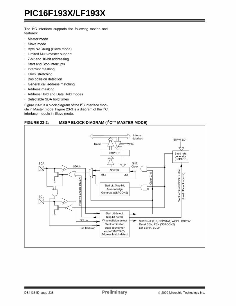
PIC16F193X/LF193X
The I2C interface supports the following modes andfeatures:
• Master mode
• Slave mode
• Byte NACKing (Slave mode)
• Limited Multi-master support
• 7-bit and 10-bit addressing
• Start and Stop interrupts
• Interrupt masking
• Clock stretching
• Bus collision detection
• General call address matching
• Address masking
• Address Hold and Data Hold modes
• Selectable SDA hold times
Figure 23-2 is a block diagram of the I2C interface mod-ule in Master mode. Figure 23-3 is a diagram of the I2Cinterface module in Slave mode.
FIGURE 23-2: MSSP BLOCK DIAGRAM (I2C™ MASTER MODE)
Read Write
SSPSR
Start bit, Stop bit,
Start bit detect,
SSPBUF
Internaldata bus
Set/Reset: S, P, SSPSTAT, WCOL, SSPOV
ShiftClock
MSb LSb
SDA
AcknowledgeGenerate (SSPCON2)
Stop bit detectWrite collision detect
Clock arbitrationState counter forend of XMIT/RCV
SCL
SCL in
Bus Collision
SDA in
Rec
eive
Ena
ble
(RC
EN
)
Clo
ck C
ntl
Clo
ck a
rbitr
ate/
BC
OL
de
tect
(Hol
d o
ff cl
ock
sou
rce
)
[SSPM 3:0]
Baud rate
Reset SEN, PEN (SSPCON2)
generator(SSPADD)
Address Match detect
Set SSPIF, BCLIF
DS41364D-page 238 Preliminary 2009 Microchip Technology Inc.
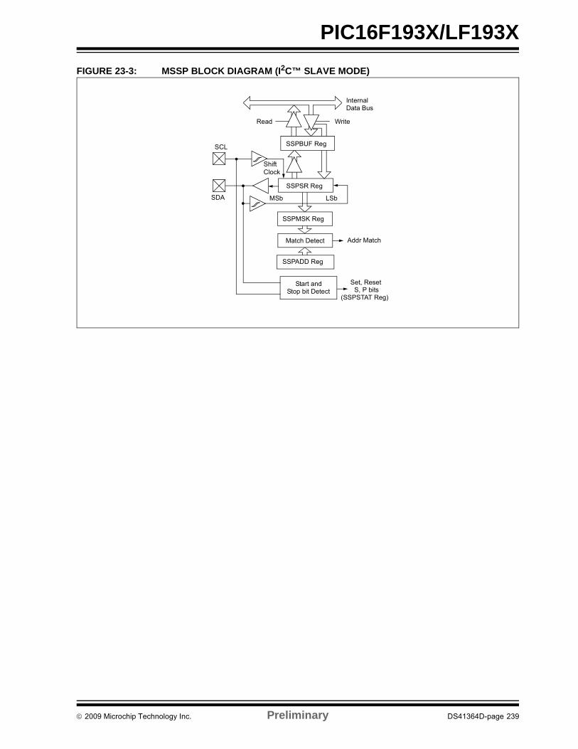
PIC16F193X/LF193X
FIGURE 23-3: MSSP BLOCK DIAGRAM (I2C™ SLAVE MODE)
Read Write
SSPSR Reg
Match Detect
SSPADD Reg
Start andStop bit Detect
SSPBUF Reg
InternalData Bus
Addr Match
Set, ResetS, P bits
(SSPSTAT Reg)
SCL
SDA
ShiftClock
MSb LSb
SSPMSK Reg
2009 Microchip Technology Inc. Preliminary DS41364D-page 239
PIC16F193X/LF193X
23.2 SPI Mode Overview
The Serial Peripheral Interface (SPI) bus is asynchronous serial data communication bus thatoperates in Full Duplex mode. Devices communicate ina master/slave environment where the master deviceinitiates the communication. A slave device iscontrolled through a chip select known as Slave Select.
The SPI bus specifies four signal connections:
• Serial Clock (SCK)
• Serial Data Out (SDO)
• Serial Data In (SDI)
• Slave Select (SS)
Figure 23-1 shows the block diagram of the MSSPmodule when operating in SPI Mode.
The SPI bus operates with a single master device andone or more slave devices. When multiple slavedevices are used, an independent Slave Select con-nection is required from the master device to eachslave device.
Figure 23-4 shows a typical connection between amaster device and multiple slave devices.
The master selects only one slave at a time. Most slavedevices have tri-state outputs so their output signalappears disconnected from the bus when they are notselected.
Transmissions involve two shift registers, eight bits insize, one in the master and one in the slave. With eitherthe master or the slave device, data is always shiftedout one bit at a time, with the Most Significant bit (MSb)shifted out first. At the same time, a new LeastSignificant bit (LSb) is shifted into the same register.
Figure 23-5 shows a typical connection between twoprocessors configured as master and slave devices.
Data is shifted out of both shift registers on the pro-grammed clock edge and latched on the opposite edgeof the clock.
The master device transmits information out on it’sSDO output pin which is connected to, and received by,the slave’s SDI input pin. The slave device transmitsinformation out on it’s SDO output pin, which is con-nected to, and received by, the master’s SDI input pin.
To begin communication, the master device first sendsout the clock signal. Both the master and the slavedevices should be configured for the same clock polar-ity.
The master device starts a transmission by sending outthe MSb from it’s shift register. The slave device readsthis bit from that same line and saves it into the LSbposition of it’s shift register.
During each SPI clock cycle, a full duplex datatransmission occurs. This means that while the masterdevice is sending out the MSb from it’s shift register (onit’s SDO pin) and the slave device is reading this bit and
saving it as the LSb of it’s shift register, that the slavedevice is also sending out the MSb from it’s shiftregister (on it’s SDO pin) and the master device isreading this bit and saving it as the LSb of it’s shiftregister.
After 8 bits have been shifted out, the master and slavehave exchanged register values.
If there is more data to exchange, the shift registers areloaded with new data and the process repeats itself.
Whether the data is meaningful or not (dummy data),depends on the application software. This leads tothree scenarios for data transmission:
• Master sends useful data and slave sends dummy data.
• Master sends useful data and slave sends useful data.
• Master sends dummy data and slave sends useful data.
Transmissions may involve any number of clockcycles. When there is no more data to be transmitted,the master stops sending the clock signal and it dese-lects the slave.
Every slave device connected to the bus that has notbeen selected through its slave select line must disre-gard the clock and transmission signals and must nottransmit out any data of it’s own.
DS41364D-page 240 Preliminary 2009 Microchip Technology Inc.

PIC16F193X/LF193X
FIGURE 23-4: SPI MASTER AND MULTIPLE SLAVE CONNECTION
23.2.1 SPI MODE REGISTERS
The MSSP module has five registers for SPI modeoperation. These are:
• MSSP STATUS register (SSPSTAT)
• MSSP Control Register 1 (SSPCON1)
• MSSP Control Register 3 (SSPCON3)
• MSSP Data Buffer register (SSPBUF)
• MSSP Address register (SSPADD)
• MSSP Shift register (SSPSR) (Not directly accessible)
SSPCON1 and SSPSTAT are the control and STATUSregisters in SPI mode operation. The SSPCON1 regis-ter is readable and writable. The lower 6 bits of theSSPSTAT are read-only. The upper two bits of theSSPSTAT are read/write.
In one SPI master mode, SSPADD can be loaded witha value used in the Baud Rate Generator. More infor-mation on the Baud Rate Generator is available inSection 23.7 “Baud Rate Generator”.
SSPSR is the shift register used for shifting data in andout. SSPBUF provides indirect access to the SSPSRregister. SSPBUF is the buffer register to which databytes are written, and from which data bytes are read.
In receive operations, SSPSR and SSPBUF togethercreate a buffered receiver. When SSPSR receives acomplete byte, it is transferred to SSPBUF and theSSPIF interrupt is set.
During transmission, the SSPBUF is not buffered. Awrite to SSPBUF will write to both SSPBUF andSSPSR.
SPI MasterSCK
SDO
SDI
General I/O
General I/O
General I/O
SCK
SDI
SDO
SS
SPI Slave#1
SCK
SDI
SDO
SS
SPI Slave#2
SCK
SDI
SDO
SS
SPI Slave#3
2009 Microchip Technology Inc. Preliminary DS41364D-page 241
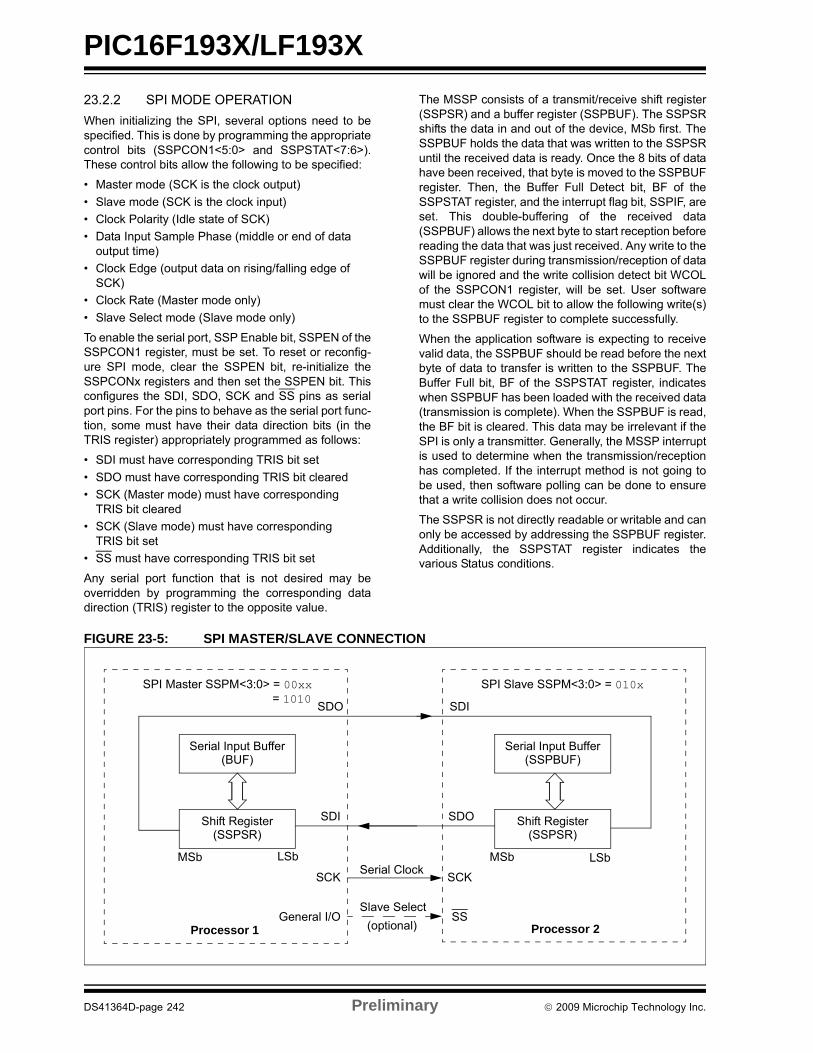
PIC16F193X/LF193X
23.2.2 SPI MODE OPERATION
When initializing the SPI, several options need to bespecified. This is done by programming the appropriatecontrol bits (SSPCON1<5:0> and SSPSTAT<7:6>).These control bits allow the following to be specified:
• Master mode (SCK is the clock output)
• Slave mode (SCK is the clock input)
• Clock Polarity (Idle state of SCK)
• Data Input Sample Phase (middle or end of data output time)
• Clock Edge (output data on rising/falling edge of SCK)
• Clock Rate (Master mode only)
• Slave Select mode (Slave mode only)
To enable the serial port, SSP Enable bit, SSPEN of theSSPCON1 register, must be set. To reset or reconfig-ure SPI mode, clear the SSPEN bit, re-initialize theSSPCONx registers and then set the SSPEN bit. Thisconfigures the SDI, SDO, SCK and SS pins as serialport pins. For the pins to behave as the serial port func-tion, some must have their data direction bits (in theTRIS register) appropriately programmed as follows:
• SDI must have corresponding TRIS bit set
• SDO must have corresponding TRIS bit cleared
• SCK (Master mode) must have corresponding TRIS bit cleared
• SCK (Slave mode) must have corresponding TRIS bit set
• SS must have corresponding TRIS bit set
Any serial port function that is not desired may beoverridden by programming the corresponding datadirection (TRIS) register to the opposite value.
The MSSP consists of a transmit/receive shift register(SSPSR) and a buffer register (SSPBUF). The SSPSRshifts the data in and out of the device, MSb first. TheSSPBUF holds the data that was written to the SSPSRuntil the received data is ready. Once the 8 bits of datahave been received, that byte is moved to the SSPBUFregister. Then, the Buffer Full Detect bit, BF of theSSPSTAT register, and the interrupt flag bit, SSPIF, areset. This double-buffering of the received data(SSPBUF) allows the next byte to start reception beforereading the data that was just received. Any write to theSSPBUF register during transmission/reception of datawill be ignored and the write collision detect bit WCOLof the SSPCON1 register, will be set. User softwaremust clear the WCOL bit to allow the following write(s)to the SSPBUF register to complete successfully.
When the application software is expecting to receivevalid data, the SSPBUF should be read before the nextbyte of data to transfer is written to the SSPBUF. TheBuffer Full bit, BF of the SSPSTAT register, indicateswhen SSPBUF has been loaded with the received data(transmission is complete). When the SSPBUF is read,the BF bit is cleared. This data may be irrelevant if theSPI is only a transmitter. Generally, the MSSP interruptis used to determine when the transmission/receptionhas completed. If the interrupt method is not going tobe used, then software polling can be done to ensurethat a write collision does not occur.
The SSPSR is not directly readable or writable and canonly be accessed by addressing the SSPBUF register.Additionally, the SSPSTAT register indicates thevarious Status conditions.
FIGURE 23-5: SPI MASTER/SLAVE CONNECTION
Serial Input Buffer(BUF)
Shift Register(SSPSR)
MSb LSb
SDO
SDI
Processor 1
SCK
SPI Master SSPM<3:0> = 00xx
Serial Input Buffer(SSPBUF)
Shift Register(SSPSR)
LSbMSb
SDI
SDO
Processor 2
SCK
SPI Slave SSPM<3:0> = 010x
Serial Clock
SSSlave Select
General I/O(optional)
= 1010
DS41364D-page 242 Preliminary 2009 Microchip Technology Inc.
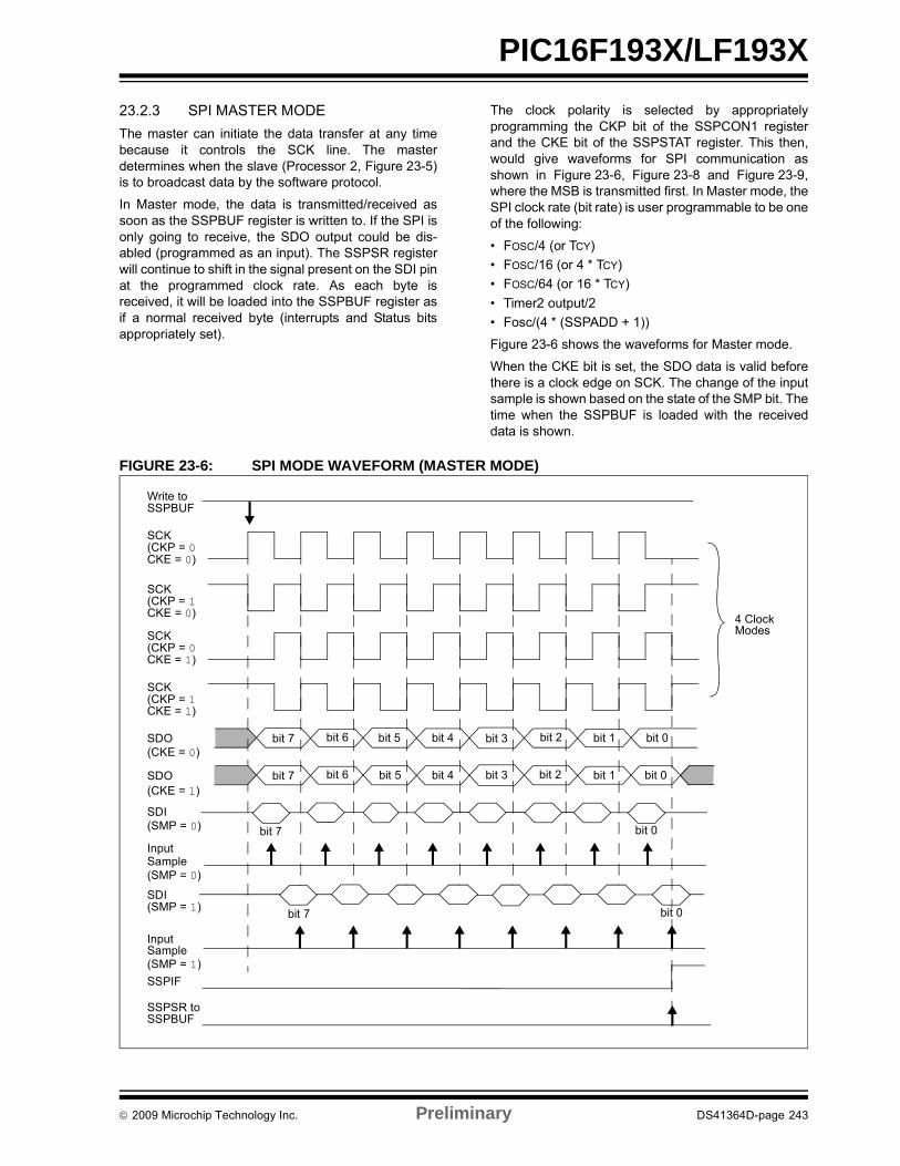
PIC16F193X/LF193X
23.2.3 SPI MASTER MODE
The master can initiate the data transfer at any timebecause it controls the SCK line. The masterdetermines when the slave (Processor 2, Figure 23-5)is to broadcast data by the software protocol.
In Master mode, the data is transmitted/received assoon as the SSPBUF register is written to. If the SPI isonly going to receive, the SDO output could be dis-abled (programmed as an input). The SSPSR registerwill continue to shift in the signal present on the SDI pinat the programmed clock rate. As each byte isreceived, it will be loaded into the SSPBUF register asif a normal received byte (interrupts and Status bitsappropriately set).
The clock polarity is selected by appropriatelyprogramming the CKP bit of the SSPCON1 registerand the CKE bit of the SSPSTAT register. This then,would give waveforms for SPI communication asshown in Figure 23-6, Figure 23-8 and Figure 23-9,where the MSB is transmitted first. In Master mode, theSPI clock rate (bit rate) is user programmable to be oneof the following:
• FOSC/4 (or TCY)
• FOSC/16 (or 4 * TCY)
• FOSC/64 (or 16 * TCY)
• Timer2 output/2
• Fosc/(4 * (SSPADD + 1))
Figure 23-6 shows the waveforms for Master mode.
When the CKE bit is set, the SDO data is valid beforethere is a clock edge on SCK. The change of the inputsample is shown based on the state of the SMP bit. Thetime when the SSPBUF is loaded with the receiveddata is shown.
FIGURE 23-6: SPI MODE WAVEFORM (MASTER MODE)
SCK(CKP = 0
SCK(CKP = 1
SCK(CKP = 0
SCK(CKP = 1
4 ClockModes
InputSample
InputSample
SDI
bit 7 bit 0
SDO bit 7 bit 6 bit 5 bit 4 bit 3 bit 2 bit 1 bit 0
bit 7
SDI
SSPIF
(SMP = 1)
(SMP = 0)
(SMP = 1)
CKE = 1)
CKE = 0)
CKE = 1)
CKE = 0)
(SMP = 0)
Write toSSPBUF
SSPSR toSSPBUF
SDO bit 7 bit 6 bit 5 bit 4 bit 3 bit 2 bit 1 bit 0
(CKE = 0)
(CKE = 1)
bit 0
2009 Microchip Technology Inc. Preliminary DS41364D-page 243
PIC16F193X/LF193X
23.2.4 SPI SLAVE MODE
In Slave mode, the data is transmitted and received asexternal clock pulses appear on SCK. When the lastbit is latched, the SSPIF interrupt flag bit is set.
Before enabling the module in SPI Slave mode, the clockline must match the proper Idle state. The clock line canbe observed by reading the SCK pin. The Idle state isdetermined by the CKP bit of the SSPCON1 register.
While in Slave mode, the external clock is supplied bythe external clock source on the SCK pin. This externalclock must meet the minimum high and low times asspecified in the electrical specifications.
While in Sleep mode, the slave can transmit/receivedata. The shift register is clocked from the SCK pininput and when a byte is received, the device will gen-erate an interrupt. If enabled, the device will wake-upfrom Sleep.
23.2.4.1 Daisy-Chain Configuration
The SPI bus can sometimes be connected in adaisy-chain configuration. The first slave output isconnected to the second slave input, the second slaveoutput is connected to the third slave input, and so on.The final slave output is connected to the master input.Each slave sends out, during a second group of clockpulses, an exact copy of what was received during thefirst group of clock pulses. The whole chain acts as onelarge communication shift register. The daisy-chainfeature only requires a single Slave Select line from themaster device.
Figure 23-7 shows the block diagram of a typicalDaisy-Chain connection when operating in SPI Mode.
In a daisy-chain configuration, only the most recentbyte on the bus is required by the slave. Setting theBOEN bit of the SSPCON3 register will enable writesto the SSPBUF register, even if the previous byte hasnot been read. This allows the software to ignore datathat may not apply to it.
23.2.5 SLAVE SELECT SYNCHRONIZATION
The Slave Select can also be used to synchronize com-munication. The Slave Select line is held high until themaster device is ready to communicate. When theSlave Select line is pulled low, the slave knows that anew transmission is starting.
If the slave fails to receive the communication properly,it will be reset at the end of the transmission, when theSlave Select line returns to a high state. The slave isthen ready to receive a new transmission when theSlave Select line is pulled low again. If the Slave Selectline is not used, there is a risk that the slave will even-tually become out of sync with the master. If the slavemisses a bit, it will always be one bit off in future trans-missions. Use of the Slave Select line allows the slaveand master to align themselves at the beginning ofeach transmission.
The SS pin allows a Synchronous Slave mode. TheSPI must be in Slave mode with SS pin control enabled(SSPCON1<3:0> = 0100).
When the SS pin is low, transmission and reception areenabled and the SDO pin is driven.
When the SS pin goes high, the SDO pin is no longerdriven, even if in the middle of a transmitted byte andbecomes a floating output. External pull-up/pull-downresistors may be desirable depending on the applica-tion.
When the SPI module resets, the bit counter is forcedto ‘0’. This can be done by either forcing the SS pin toa high level or clearing the SSPEN bit.
Note 1: When the SPI is in Slave mode with SS pincontrol enabled (SSPCON1<3:0> =0100), the SPI module will reset if the SSpin is set to VDD.
2: When the SPI is used in Slave mode withCKE set; the user must enable SS pincontrol.
3: While operated in SPI Slave mode theSMP bit of the SSPSTAT register mustremain clear.
DS41364D-page 244 Preliminary 2009 Microchip Technology Inc.
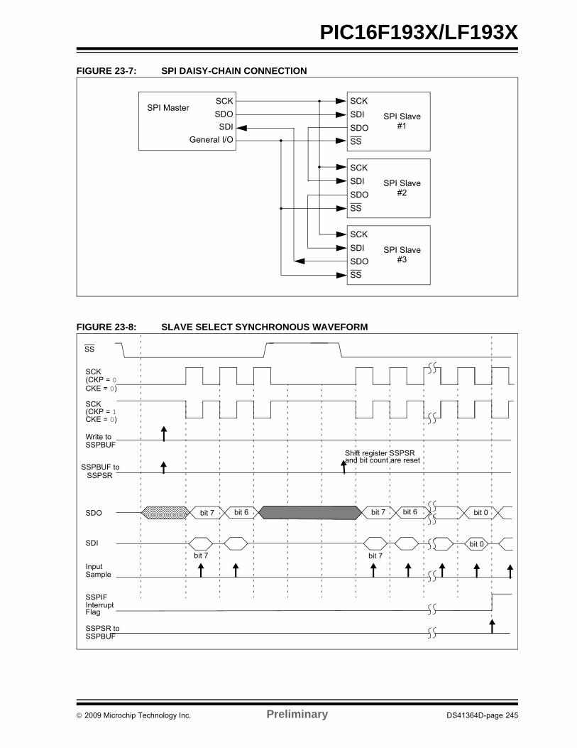
PIC16F193X/LF193X
FIGURE 23-7: SPI DAISY-CHAIN CONNECTION
FIGURE 23-8: SLAVE SELECT SYNCHRONOUS WAVEFORM
SPI MasterSCK
SDO
SDI
General I/O
SCK
SDI
SDO
SS
SPI Slave#1
SCK
SDI
SDO
SS
SPI Slave#2
SCK
SDI
SDO
SS
SPI Slave#3
SCK(CKP = 1
SCK(CKP = 0
InputSample
SDI
bit 7
SDO bit 7 bit 6 bit 7
SSPIFInterrupt
CKE = 0)
CKE = 0)
Write toSSPBUF
SSPSR toSSPBUF
SS
Flag
bit 0
bit 7
bit 0
bit 6
SSPBUF toSSPSR
Shift register SSPSRand bit count are reset
2009 Microchip Technology Inc. Preliminary DS41364D-page 245
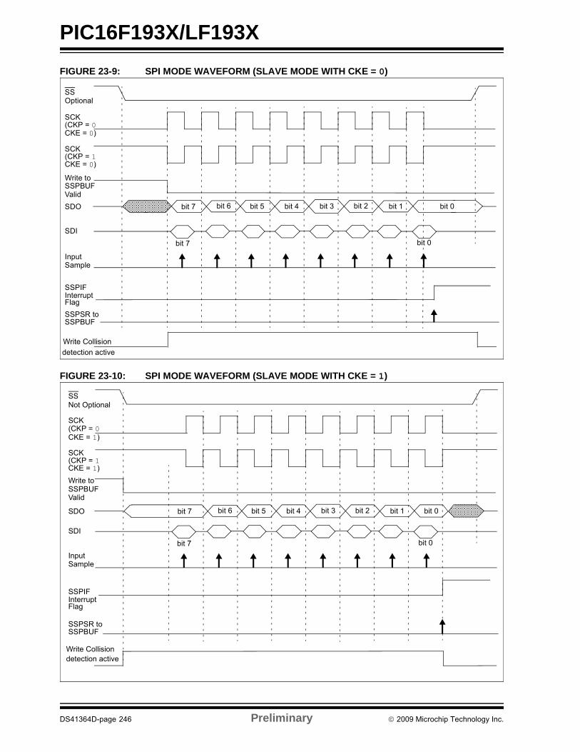
PIC16F193X/LF193X
FIGURE 23-9: SPI MODE WAVEFORM (SLAVE MODE WITH CKE = 0)
FIGURE 23-10: SPI MODE WAVEFORM (SLAVE MODE WITH CKE = 1)
SCK(CKP = 1
SCK(CKP = 0
InputSample
SDI
bit 7
SDO bit 7 bit 6 bit 5 bit 4 bit 3 bit 2 bit 1 bit 0
SSPIFInterrupt
CKE = 0)
CKE = 0)
Write toSSPBUF
SSPSR toSSPBUF
SS
Flag
Optional
bit 0
detection active
Write Collision
Valid
SCK(CKP = 1
SCK(CKP = 0
InputSample
SDI
bit 7 bit 0
SDO bit 7 bit 6 bit 5 bit 4 bit 3 bit 2 bit 1 bit 0
SSPIFInterrupt
CKE = 1)
CKE = 1)
Write toSSPBUF
SSPSR toSSPBUF
SS
Flag
Not Optional
Write Collisiondetection active
Valid
DS41364D-page 246 Preliminary 2009 Microchip Technology Inc.
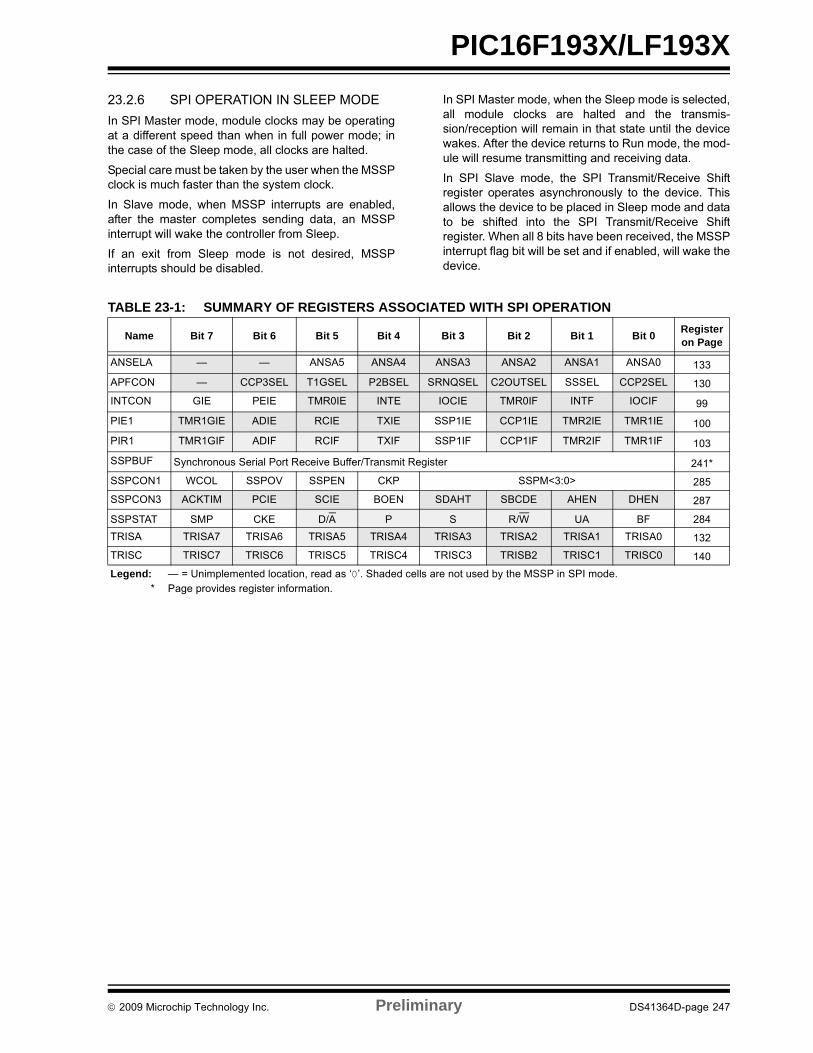
PIC16F193X/LF193X
23.2.6 SPI OPERATION IN SLEEP MODE
In SPI Master mode, module clocks may be operatingat a different speed than when in full power mode; inthe case of the Sleep mode, all clocks are halted.
Special care must be taken by the user when the MSSPclock is much faster than the system clock.
In Slave mode, when MSSP interrupts are enabled,after the master completes sending data, an MSSPinterrupt will wake the controller from Sleep.
If an exit from Sleep mode is not desired, MSSPinterrupts should be disabled.
In SPI Master mode, when the Sleep mode is selected,all module clocks are halted and the transmis-sion/reception will remain in that state until the devicewakes. After the device returns to Run mode, the mod-ule will resume transmitting and receiving data.
In SPI Slave mode, the SPI Transmit/Receive Shiftregister operates asynchronously to the device. Thisallows the device to be placed in Sleep mode and datato be shifted into the SPI Transmit/Receive Shiftregister. When all 8 bits have been received, the MSSPinterrupt flag bit will be set and if enabled, will wake thedevice.
TABLE 23-1: SUMMARY OF REGISTERS ASSOCIATED WITH SPI OPERATION
Name Bit 7 Bit 6 Bit 5 Bit 4 Bit 3 Bit 2 Bit 1 Bit 0Register on Page
ANSELA — — ANSA5 ANSA4 ANSA3 ANSA2 ANSA1 ANSA0 133
APFCON — CCP3SEL T1GSEL P2BSEL SRNQSEL C2OUTSEL SSSEL CCP2SEL 130
INTCON GIE PEIE TMR0IE INTE IOCIE TMR0IF INTF IOCIF 99
PIE1 TMR1GIE ADIE RCIE TXIE SSP1IE CCP1IE TMR2IE TMR1IE 100
PIR1 TMR1GIF ADIF RCIF TXIF SSP1IF CCP1IF TMR2IF TMR1IF 103
SSPBUF Synchronous Serial Port Receive Buffer/Transmit Register 241*
SSPCON1 WCOL SSPOV SSPEN CKP SSPM<3:0> 285
SSPCON3 ACKTIM PCIE SCIE BOEN SDAHT SBCDE AHEN DHEN 287
SSPSTAT SMP CKE D/A P S R/W UA BF 284
TRISA TRISA7 TRISA6 TRISA5 TRISA4 TRISA3 TRISA2 TRISA1 TRISA0 132
TRISC TRISC7 TRISC6 TRISC5 TRISC4 TRISC3 TRISB2 TRISC1 TRISC0 140
Legend: — = Unimplemented location, read as ‘0’. Shaded cells are not used by the MSSP in SPI mode.* Page provides register information.
2009 Microchip Technology Inc. Preliminary DS41364D-page 247

PIC16F193X/LF193X
23.3 I2C Mode Overview
The Inter-Integrated Circuit Bus (I²C) is a multi-masterserial data communication bus. Devices communicatein a master/slave environment where the masterdevices initiate the communication. A Slave device iscontrolled through addressing.
The I2C bus specifies two signal connections:
• Serial Clock (SCL)
• Serial Data (SDA)
Figure 23-11 shows the block diagram of the MSSPmodule when operating in I2C Mode.
Both the SCL and SDA connections are bidirectionalopen-drain lines, each requiring pull-up resistors for thesupply voltage. Pulling the line to ground is considereda logical zero and letting the line float is considered alogical one.
Figure 23-11 shows a typical connection between twoprocessors configured as master and slave devices.
The I2C bus can operate with one or more masterdevices and one or more slave devices.
There are four potential modes of operation for a givendevice:
• Master Transmit mode(master is transmitting data to a slave)
• Master Receive mode(master is receiving data from a slave)
• Slave Transmit mode(slave is transmitting data to a master)
• Slave Receive mode(slave is receiving data from the master)
To begin communication, a master device starts out inMaster Transmit mode. The master device sends out aStart bit followed by the address byte of the slave itintends to communicate with. This is followed by a sin-gle Read/Write bit, which determines whether the mas-ter intends to transmit to or receive data from the slavedevice.
If the requested slave exists on the bus, it will respondwith an Acknowledge bit, otherwise known as an ACK.The master then continues in either Transmit mode orReceive mode and the slave continues in the comple-ment, either in Receive mode or Transmit mode,respectively.
A Start bit is indicated by a high-to-low transition of theSDA line while the SCL line is held high. Address anddata bytes are sent out, Most Significant bit (MSb) first.The Read/Write bit is sent out as a logical one when themaster intends to read data from the slave, and is sentout as a logical zero when it intends to write data to theslave.
FIGURE 23-11: I2C MASTER/SLAVE CONNECTION
The Acknowledge bit (ACK) is an active-low signal,which holds the SDA line low to indicate to the transmit-ter that the slave device has received the transmitteddata and is ready to receive more.
The transition of a data bit is always performed whilethe SCL line is held low. Transitions that occur while theSCL line is held high are used to indicate Start and Stopbits.
If the master intends to write to the slave, then it repeat-edly sends out a byte of data, with the slave respondingafter each byte with an ACK bit. In this example, themaster device is in Master Transmit mode and theslave is in Slave Receive mode.
If the master intends to read from the slave, then itrepeatedly receives a byte of data from the slave, andresponds after each byte with an ACK bit. In this exam-ple, the master device is in Master Receive mode andthe slave is Slave Transmit mode.
On the last byte of data communicated, the masterdevice may end the transmission by sending a Stop bit.If the master device is in Receive mode, it sends theStop bit in place of the last ACK bit. A Stop bit is indi-cated by a low-to-high transition of the SDA line whilethe SCL line is held high.
In some cases, the master may want to maintain con-trol of the bus and re-initiate another transmission. Ifso, the master device may send another Start bit inplace of the Stop bit or last ACK bit when it is in receivemode.
The I2C bus specifies three message protocols;
• Single message where a master writes data to a slave.
• Single message where a master reads data from a slave.
• Combined message where a master initiates a minimum of two writes, or two reads, or a combination of writes and reads, to one or more slaves.
Master
SCL
SDA
SCL
SDA
SlaveVDD
VDD
DS41364D-page 248 Preliminary 2009 Microchip Technology Inc.
PIC16F193X/LF193X
When one device is transmitting a logical one, or lettingthe line float, and a second device is transmitting a log-ical zero, or holding the line low, the first device candetect that the line is not a logical one. This detection,when used on the SCL line, is called clock stretching.Clock stretching gives slave devices a mechanism tocontrol the flow of data. When this detection is used onthe SDA line, it is called arbitration. Arbitration ensuresthat there is only one master device communicating atany single time.
23.3.1 CLOCK STRETCHING
When a slave device has not completed processingdata, it can delay the transfer of more data through theprocess of Clock Stretching. An addressed slavedevice may hold the SCL clock line low after receivingor sending a bit, indicating that it is not yet ready to con-tinue. The master that is communicating with the slavewill attempt to raise the SCL line in order to transfer thenext bit, but will detect that the clock line has not yetbeen released. Because the SCL connection isopen-drain, the slave has the ability to hold that line lowuntil it is ready to continue communicating.
Clock stretching allows receivers that cannot keep upwith a transmitter to control the flow of incoming data.
23.3.2 ARBITRATION
Each master device must monitor the bus for Start andStop bits. If the device detects that the bus is busy, itcannot begin a new message until the bus returns to anIdle state.
However, two master devices may try to initiate a trans-mission on or about the same time. When this occurs,the process of arbitration begins. Each transmitterchecks the level of the SDA data line and compares itto the level that it expects to find. The first transmitter toobserve that the two levels don’t match, loses arbitra-tion, and must stop transmitting on the SDA line.
For example, if one transmitter holds the SDA line to alogical one (lets it float) and a second transmitter holdsit to a logical zero (pulls it low), the result is that theSDA line will be low. The first transmitter then observesthat the level of the line is different than expected andconcludes that another transmitter is communicating.
The first transmitter to notice this difference is the onethat loses arbitration and must stop driving the SDAline. If this transmitter is also a master device, it alsomust stop driving the SCL line. It then can monitor thelines for a Stop condition before trying to reissue itstransmission. In the meantime, the other device thathas not noticed any difference between the expectedand actual levels on the SDA line continues with it’soriginal transmission. It can do so without any compli-cations, because so far, the transmission appearsexactly as expected with no other transmitter disturbingthe message.
Slave Transmit mode can also be arbitrated, when amaster addresses multiple slaves, but this is less com-mon.
If two master devices are sending a message to two dif-ferent slave devices at the address stage, the mastersending the lower slave address always wins arbitra-tion. When two master devices send messages to thesame slave address, and addresses can sometimesrefer to multiple slaves, the arbitration process mustcontinue into the data stage.
Arbitration usually occurs very rarely, but it is a neces-sary process for proper multi-master support.
23.4 I2C™ Mode Operation
All MSSP I2C communication is byte oriented andshifted out MSb first. Six SFR registers and 2 interruptflags interface the module with the PIC® microcon-troller and user software. Two pins, SDA and SCL, areexercised by the module to communicate with otherexternal I2C devices.
23.4.1 BYTE FORMAT
All communication in I2C is done in 9-bit segments. Abyte is sent from a Master to a Slave or vice-versa, fol-lowed by an Acknowledge bit sent back. After the 8thfalling edge of the SCL line, the device outputting dataon the SDA changes that pin to an input and reads inan acknowledge value on the next clock pulse.
The clock signal, SCL, is provided by the master. Datais valid to change while the SCL signal is low, andsampled on the rising edge of the clock. Changes onthe SDA line while the SCL line is high define specialconditions on the bus, explained below.
23.4.2 DEFINITION OF I2C TERMINOLOGY
There is language and terminology in the descriptionof I2C communication that have definitions specific toI2C. That word usage is defined below and may beused in the rest of this document without explana-tion. This table was adapted from the Phillips I2Cspecification.
23.4.3 SDA AND SCL PINS
Selection of any I2C mode with the SSPEN bit set,forces the SCL and SDA pins to be open-drain. Thesepins should be set by the user to inputs by setting theappropriate TRIS bits.
23.4.4 SDA HOLD TIME
The hold time of the SDA pin is selected by the SDAHTbit of the SSPCON3 register. Hold time is the time SDAis held valid after the falling edge of SCL. Setting theSDAHT bit selects a longer 300 ns minimum hold timeand may help on buses with large capacitance.
Note: Data is tied to output zero when an I2C modeis enabled.
2009 Microchip Technology Inc. Preliminary DS41364D-page 249
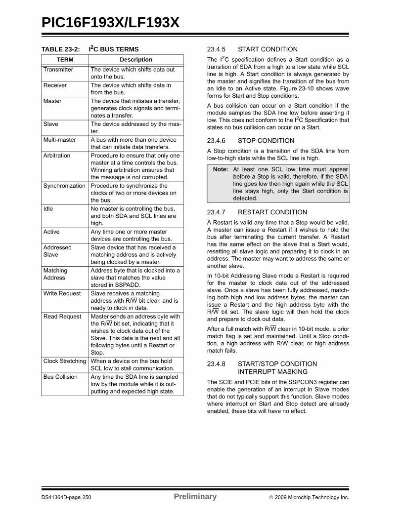
PIC16F193X/LF193X
TABLE 23-2: I2C BUS TERMS 23.4.5 START CONDITION
The I2C specification defines a Start condition as atransition of SDA from a high to a low state while SCLline is high. A Start condition is always generated bythe master and signifies the transition of the bus froman Idle to an Active state. Figure 23-10 shows waveforms for Start and Stop conditions.
A bus collision can occur on a Start condition if themodule samples the SDA line low before asserting itlow. This does not conform to the I2C Specification thatstates no bus collision can occur on a Start.
23.4.6 STOP CONDITION
A Stop condition is a transition of the SDA line fromlow-to-high state while the SCL line is high.
23.4.7 RESTART CONDITION
A Restart is valid any time that a Stop would be valid.A master can issue a Restart if it wishes to hold thebus after terminating the current transfer. A Restarthas the same effect on the slave that a Start would,resetting all slave logic and preparing it to clock in anaddress. The master may want to address the same oranother slave.
In 10-bit Addressing Slave mode a Restart is requiredfor the master to clock data out of the addressedslave. Once a slave has been fully addressed, match-ing both high and low address bytes, the master canissue a Restart and the high address byte with theR/W bit set. The slave logic will then hold the clockand prepare to clock out data.
After a full match with R/W clear in 10-bit mode, a priormatch flag is set and maintained. Until a Stop condi-tion, a high address with R/W clear, or high addressmatch fails.
23.4.8 START/STOP CONDITION INTERRUPT MASKING
The SCIE and PCIE bits of the SSPCON3 register canenable the generation of an interrupt in Slave modesthat do not typically support this function. Slave modeswhere interrupt on Start and Stop detect are alreadyenabled, these bits will have no effect.
TERM Description
Transmitter The device which shifts data out onto the bus.
Receiver The device which shifts data in from the bus.
Master The device that initiates a transfer, generates clock signals and termi-nates a transfer.
Slave The device addressed by the mas-ter.
Multi-master A bus with more than one device that can initiate data transfers.
Arbitration Procedure to ensure that only one master at a time controls the bus. Winning arbitration ensures that the message is not corrupted.
Synchronization Procedure to synchronize the clocks of two or more devices on the bus.
Idle No master is controlling the bus, and both SDA and SCL lines are high.
Active Any time one or more master devices are controlling the bus.
Addressed Slave
Slave device that has received a matching address and is actively being clocked by a master.
Matching Address
Address byte that is clocked into a slave that matches the value stored in SSPADD.
Write Request Slave receives a matching address with R/W bit clear, and is ready to clock in data.
Read Request Master sends an address byte with the R/W bit set, indicating that it wishes to clock data out of the Slave. This data is the next and all following bytes until a Restart or Stop.
Clock Stretching When a device on the bus hold SCL low to stall communication.
Bus Collision Any time the SDA line is sampled low by the module while it is out-putting and expected high state.
Note: At least one SCL low time must appearbefore a Stop is valid, therefore, if the SDAline goes low then high again while the SCLline stays high, only the Start condition isdetected.
DS41364D-page 250 Preliminary 2009 Microchip Technology Inc.

PIC16F193X/LF193X
FIGURE 23-12: I2C START AND STOP CONDITIONS
FIGURE 23-13: I2C RESTART CONDITION
SDA
SCL
P
Stop
Condition
S
Start
Condition
Change of
Data Allowed
Change of
Data Allowed
Restart
Condition
Sr
Change of
Data AllowedChange of
Data Allowed
2009 Microchip Technology Inc. Preliminary DS41364D-page 251

PIC16F193X/LF193X
23.4.9 ACKNOWLEDGE SEQUENCE
The 9th SCL pulse for any transferred byte in I2C isdedicated as an Acknowledge. It allows receivingdevices to respond back to the transmitter by pullingthe SDA line low. The transmitter must release controlof the line during this time to shift in the response. TheAcknowledge (ACK) is an active-low signal, pulling theSDA line low indicated to the transmitter that thedevice has received the transmitted data and is readyto receive more.
The result of an ACK is placed in the ACKSTAT bit ofthe SSPCON2 register.
Slave software, when the AHEN and DHEN bits areset, allow the user to set the ACK value sent back tothe transmitter. The ACKDT bit of the SSPCON2 regis-ter is set/cleared to determine the response.
Slave hardware will generate an ACK response if theAHEN and DHEN bits of the SSPCON3 register areclear.
There are certain conditions where an ACK will not besent by the slave. If the BF bit of the SSPSTAT registeror the SSPOV bit of the SSPCON1 register are setwhen a byte is received.
When the module is addressed, after the 8th fallingedge of SCL on the bus, the ACKTIM bit of theSSPCON3 register is set. The ACKTIM bit indicatesthe acknowledge time of the active bus. The ACKTIMStatus bit is only active when the AHEN bit or DHENbit is enabled.
23.5 I2C Slave Mode Operation
The MSSP Slave mode operates in one of four modesselected in the SSPM bits of SSPCON1 register. Themodes can be divided into 7-bit and 10-bit Addressingmode. 10-bit Addressing modes operate the same as7-bit with some additional overhead for handling thelarger addresses.
Modes with Start and Stop bit interrupts operated thesame as the other modes with SSPIF additionally get-ting set upon detection of a Start, Restart, or Stopcondition.
23.5.1 SLAVE MODE ADDRESSES
The SSPADD register (Register 23-6) contains theSlave mode address. The first byte received after aStart or Restart condition is compared against thevalue stored in this register. If the byte matches, thevalue is loaded into the SSPBUF register and an inter-rupt is generated. If the value does not match, themodule goes idle and no indication is given to the soft-ware that anything happened.
The SSP Mask register (Register 23-5) affects theaddress matching process. See Section 23.5.9 “SSPMask Register” for more information.
23.5.1.1 I2C Slave 7-bit Addressing Mode
In 7-bit Addressing mode, the LSb of the received databyte is ignored when determining if there is an addressmatch.
23.5.1.2 I2C Slave 10-bit Addressing Mode
In 10-bit Addressing mode, the first received byte iscompared to the binary value of ‘1 1 1 1 0 A9 A8 0’. A9and A8 are the two MSb of the 10-bit address andstored in bits 2 and 1 of the SSPADD register.
After the acknowledge of the high byte the UA bit is setand SCL is held low until the user updates SSPADDwith the low address. The low address byte is clockedin and all 8 bits are compared to the low address valuein SSPADD. Even if there is not an address match;SSPIF and UA are set, and SCL is held low untilSSPADD is updated to receive a high byte again.When SSPADD is updated the UA bit is cleared. Thisensures the module is ready to receive the highaddress byte on the next communication.
A high and low address match as a write request isrequired at the start of all 10-bit addressing communi-cation. A transmission can be initiated by issuing aRestart once the slave is addressed, and clocking inthe high address with the R/W bit set. The slave hard-ware will then acknowledge the read request and pre-pare to clock out data. This is only valid for a slaveafter it has received a complete high and low addressbyte match.
DS41364D-page 252 Preliminary 2009 Microchip Technology Inc.
PIC16F193X/LF193X
23.5.2 SLAVE RECEPTION
When the R/W bit of a matching received address byteis clear, the R/W bit of the SSPSTAT register is cleared.The received address is loaded into the SSPBUF reg-ister and acknowledged.
When the overflow condition exists for a receivedaddress, then not Acknowledge is given. An overflowcondition is defined as either bit BF bit of the SSPSTATregister is set, or bit SSPOV bit of the SSPCON1 reg-ister is set. The BOEN bit of the SSPCON3 registermodifies this operation. For more information seeRegister 23-4.
An MSSP interrupt is generated for each transferreddata byte. Flag bit, SSPIF, must be cleared by software.
When the SEN bit of the SSPCON2 register is set, SCLwill be held low (clock stretch) following each receivedbyte. The clock must be released by setting the CKPbit of the SSPCON1 register, except sometimes in10-bit mode. See Section 23.2.3 “SPI Master Mode”for more detail.
23.5.2.1 7-bit Addressing Reception
This section describes a standard sequence of eventsfor the MSSP module configured as an I2C Slave in7-bit Addressing mode. All decisions made by hard-ware or software and their effect on reception.Figure 23-13 and Figure 23-14 is used as a visualreference for this description.
This is a step by step process of what typically mustbe done to accomplish I2C communication.
1. Start bit detected.
2. S bit of SSPSTAT is set; SSPIF is set if interrupton Start detect is enabled.
3. Matching address with R/W bit clear is received.
4. The slave pulls SDA low sending an ACK to themaster, and sets SSPIF bit.
5. Software clears the SSPIF bit.
6. Software reads received address from SSPBUFclearing the BF flag.
7. If SEN = 1; Slave software sets CKP bit torelease the SCL line.
8. The master clocks out a data byte.
9. Slave drives SDA low sending an ACK to themaster, and sets SSPIF bit.
10. Software clears SSPIF.
11. Software reads the received byte from SSPBUFclearing BF.
12. Steps 8-12 are repeated for all received bytesfrom the Master.
13. Master sends Stop condition, setting P bit ofSSPSTAT, and the bus goes idle.
23.5.2.2 7-bit Reception with AHEN and DHEN
Slave device reception with AHEN and DHEN setoperate the same as without these options with extrainterrupts and clock stretching added after the 8th fall-ing edge of SCL. These additional interrupts allow theslave software to decide whether it wants to ACK thereceive address or data byte, rather than the hard-ware. This functionality adds support for PMBus™ thatwas not present on previous versions of this module.
This list describes the steps that need to be taken byslave software to use these options for I2C commun-cation. Figure 23-15 displays a module using bothaddress and data holding. Figure 23-16 includes theoperation with the SEN bit of the SSPCON2 registerset.
1. S bit of SSPSTAT is set; SSPIF is set if interrupton Start detect is enabled.
2. Matching address with R/W bit clear is clockedin. SSPIF is set and CKP cleared after the 8thfalling edge of SCL.
3. Slave clears the SSPIF.
4. Slave can look at the ACKTIM bit of theSSPCON3 register to determine if the SSPIFwas after or before the ACK.
5. Slave reads the address value from SSPBUF,clearing the BF flag.
6. Slave sets ACK value clocked out to the masterby setting ACKDT.
7. Slave releases the clock by setting CKP.
8. SSPIF is set after an ACK, not after a NACK.
9. If SEN = 1 the slave hardware will stretch theclock after the ACK.
10. Slave clears SSPIF.
11. SSPIF set and CKP cleared after 8th fallingedge of SCL for a received data byte.
12. Slave looks at ACKTIM bit of SSPCON3 todetermine the source of the interrupt.
13. Slave reads the received data from SSPBUFclearing BF.
14. Steps 7-14 are the same for each received databyte.
15. Communication is ended by either the slavesending an ACK = 1, or the master sending aStop condition. If a Stop is sent and Interrupt onStop Detect is disabled, the slave will only knowby polling the P bit of the SSTSTAT register.
Note: SSPIF is still set after the 9th falling edge ofSCL even if there is no clock stretching andBF has been cleared. Only if NACK is sent toMaster is SSPIF not set
2009 Microchip Technology Inc. Preliminary DS41364D-page 253

PIC16F193X/LF193X
FIGURE 23-14: I2C SLAVE, 7-BIT ADDRESS, RECEPTION (SEN = 0, AHEN = 0, DHEN = 0)
Rec
eivi
ng
Ad
dre
ss
AC
K
Rec
eiv
ing
Dat
a
AC
K
Rec
eiv
ing
Dat
aA
CK
=1
A7
A6
A5
A4
A3
A2
A1
D7
D6
D5
D4
D3
D2
D1
D0
D7
D6
D5
D4
D3
D2
D1
D0
SD
A
SC
L
SS
PIF
BF
SS
PO
V
12
34
56
78
12
34
56
78
12
34
56
78
99
9
AC
K is
no
t se
nt.
SS
PO
V s
et b
ecau
seS
SP
BU
F is
stil
l fu
ll.
Cle
are
d b
y so
ftwar
e
Firs
t by
te o
f da
ta is
ava
ilabl
e in
SS
PB
UF
SS
PB
UF
is r
ead
SS
PIF
set
on
9th
falli
ng e
dge
of
SC
LC
lea
red
by s
oftw
are
P
Bu
s M
ast
er
send
s S
top
cond
ition
S
Fro
m S
lave
to M
aste
r
DS41364D-page 254 Preliminary 2009 Microchip Technology Inc.
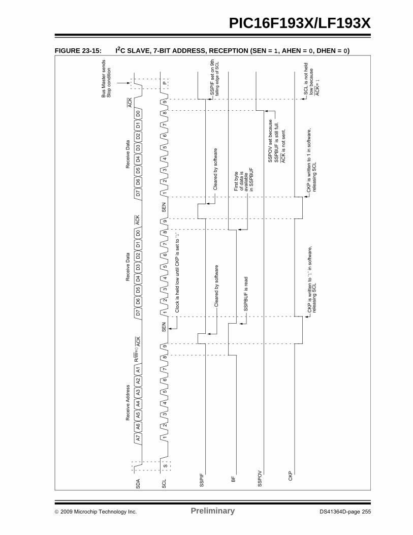
PIC16F193X/LF193X
FIGURE 23-15: I2C SLAVE, 7-BIT ADDRESS, RECEPTION (SEN = 1, AHEN = 0, DHEN = 0)
SE
NS
EN
A7
A6
A5
A4
A3
A2
A1
D7
D6
D5
D4
D3
D2
D1
D0
D7
D6
D5
D4
D3
D2
D1
D0
SD
A
SC
L1
23
45
67
89
12
34
56
78
91
23
45
67
89
P
SS
PIF
set
on
9th
SC
L is
not
hel
dC
KP
is w
ritte
n to
1 in
sof
twar
e,
CK
P is
writ
ten
to ‘1
’ in
sof
twar
e,
AC
K
low
bec
aus
e
falli
ng e
dge
of
SC
L
rele
asin
g S
CL A
CK
is n
ot s
ent.
Bus
Mas
ter
send
s
CK
P
SS
PO
V
BF
SS
PIF
SS
PO
V s
et b
eca
use
SS
PB
UF
is s
till f
ull.
Cle
are
d b
y so
ftwa
re
Firs
t byt
e o
f da
ta is
ava
ilabl
e in
SS
PB
UF
AC
K=1
Cle
ared
by
softw
are
SS
PB
UF
is r
ead
Clo
ck is
hel
d lo
w u
ntil
CK
P is
se
t to
‘1’
rele
asi
ng S
CL
Sto
p c
ondi
tion
S
AC
K
AC
KR
ecei
ve A
ddre
ssR
ecei
ve D
ata
Rec
eive
Dat
a
R/W
=0
2009 Microchip Technology Inc. Preliminary DS41364D-page 255

PIC16F193X/LF193X
FIGURE 23-16: I2C SLAVE, 7-BIT ADDRESS, RECEPTION (SEN = 0, AHEN = 1, DHEN = 1)
Rec
eiv
ing
Add
ress
Rec
eiv
ing
Dat
aR
ece
ive
d D
ata
P
A7
A6
A5
A4
A3
A2
A1
D7
D6
D5
D4
D3
D2
D1
D0
D7
D6
D5
D4
D3
D2
D1
D0
SD
A
SC
L
BF
CK
P S P
12
34
56
78
91
23
45
67
89
12
34
56
78
Ma
ster
sen
dsS
top
con
ditio
n
S
Da
ta is
re
ad f
rom
SS
PB
UF
Cle
are
d b
y so
ftwar
eS
SP
IF is
set
on
9th
falli
ng
edg
e o
f S
CL,
afte
r A
CK
CK
P s
et b
y so
ftwar
e,
SC
L is
rel
eas
ed
Sla
ve s
oftw
are
9
AC
KT
IM c
lear
ed b
yh
ard
war
e in
9th
ri
sing
edg
e o
f SC
L
sets
AC
KD
T to
not
AC
K
Whe
n D
HE
N=
1:C
KP
is c
lea
red
by
hard
wa
re o
n 8
th f
allin
ge
dge
of
SC
L
Sla
ve s
oftw
are
clea
rs A
CK
DT
to
AC
K t
he r
ecei
ved
byt
e
AC
KT
IM s
et b
y ha
rdw
are
on 8
th fa
llin
g e
dge
of
SC
L
Whe
n A
HE
N=
1:
CK
P is
cle
ared
by
har
dw
are
and
SC
L is
str
etc
hedAdd
ress
isre
ad fr
om
S
SB
UF
AC
KT
IM s
et b
y ha
rdw
are
on 8
th fa
lling
edg
e o
f SC
L
AC
K
Ma
ster
Rel
eas
es S
DA
to s
lave
for
AC
K s
equ
enc
e
No
inte
rru
pta
fter
not A
CK
from
Sla
ve
AC
K=
1A
CK
AC
KD
T
AC
KT
IM
SS
PIF
If A
HE
N=1
:S
SP
IF is
set
DS41364D-page 256 Preliminary 2009 Microchip Technology Inc.
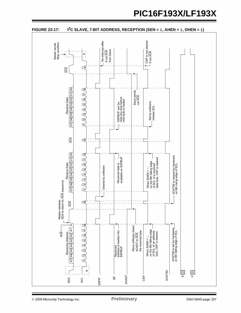
PIC16F193X/LF193X
FIGURE 23-17: I2C SLAVE, 7-BIT ADDRESS, RECEPTION (SEN = 1, AHEN = 1, DHEN = 1)
Re
ceiv
ing
Add
ress
Rec
eive
Da
taR
ece
ive
Dat
a
A7
A6
A5
A4
A3
A2
A1
D7
D6
D5
D4
D3
D2
D1
D0
D7
D6
D5
D4
D3
D2
D1
D0
SD
A
SC
L
SS
PIF B
F
AC
KD
T
CK
P S P
AC
K
S1
23
45
67
89
12
34
56
78
91
23
45
67
89
AC
K
AC
K
Cle
are
d b
y so
ftwar
e
AC
KT
IM is
cle
are
d b
y ha
rdw
are
SS
PB
UF
can
be
Set
by
softw
are
,
rea
d a
ny ti
me
bef
ore
nex
t by
te is
load
ed
rele
ase
SC
L
on 9
th r
isin
g e
dge
of
SC
L
Re
ceiv
ed
add
ress
is lo
ade
d in
to
SS
PB
UF
Sla
ve s
oftw
are
cle
ars
AC
KD
T t
o A
CK
R/W
= 0
Mas
ter
rele
ases
SD
A to
sla
ve fo
r A
CK
seq
uenc
e
the
re
ceiv
ed
byt
e
Whe
n A
HE
N=1
;on
the
8th
falli
ng
edg
eof
SC
L o
f an
add
ress
byte
, CK
P is
cle
are
d
AC
KT
IM is
set
by
har
dwar
eon
8th
fal
ling
ed
ge o
f SC
L
Whe
n D
HE
N =
1;
on t
he 8
th fa
llin
g e
dge
of S
CL
of
a re
ceiv
edda
ta b
yte,
CK
P is
cle
are
d
Re
ceiv
ed
dat
a is
ava
ilabl
e o
n S
SP
BU
F
Sla
ve s
end
sn
ot A
CK
CK
P is
not
cle
are
dif
not A
CK
P
Ma
ster
sen
dsS
top
con
ditio
n
No
inte
rru
pt a
fter
if no
t AC
Kfr
om S
lave
AC
KT
IM
2009 Microchip Technology Inc. Preliminary DS41364D-page 257

PIC16F193X/LF193X
23.5.3 SLAVE TRANSMISSION
When the R/W bit of the incoming address byte is setand an address match occurs, the R/W bit of theSSPSTAT register is set. The received address isloaded into the SSPBUF register, and an ACK pulse issent by the slave on the ninth bit.
Following the ACK, slave hardware clears the CKP bitand the SCL pin is held low (see Section 23.5.6“Clock Stretching” for more detail). By stretching theclock, the master will be unable to assert another clockpulse until the slave is done preparing the transmitdata.
The transmit data must be loaded into the SSPBUFregister which also loads the SSPSR register. Then theSCL pin should be released by setting the CKP bit ofthe SSPCON1 register. The eight data bits are shiftedout on the falling edge of the SCL input. This ensuresthat the SDA signal is valid during the SCL high time.
The ACK pulse from the master-receiver is latched onthe rising edge of the ninth SCL input pulse. This ACKvalue is copied to the ACKSTAT bit of the SSPCON2register. If ACKSTAT is set (not ACK), then the datatransfer is complete. In this case, when the not ACK islatched by the slave, the slave goes idle and waits foranother occurrence of the Start bit. If the SDA line waslow (ACK), the next transmit data must be loaded intothe SSPBUF register. Again, the SCL pin must bereleased by setting bit CKP.
An MSSP interrupt is generated for each data transferbyte. The SSPIF bit must be cleared by software andthe SSPSTAT register is used to determine the statusof the byte. The SSPIF bit is set on the falling edge ofthe ninth clock pulse.
23.5.3.1 Slave Mode Bus Collision
A slave receives a Read request and begins shiftingdata out on the SDA line. If a bus collision is detectedand the SBCDE bit of the SSPCON3 register is set, theBCLIF bit of the PIR register is set. Once a bus collisionis detected, the slave goes idle and waits to beaddressed again. User software can use the BCLIF bitto handle a slave bus collision.
23.5.3.2 7-bit Transmission
A master device can transmit a read request to aslave, and then clock data out of the slave. The listbelow outlines what software for a slave will need todo to accomplish a standard transmission.Figure 23-17 can be used as a reference to this list.
1. Master sends a Start condition on SDA andSCL.
2. S bit of SSPSTAT is set; SSPIF is set if interrupton Start detect is enabled.
3. Matching address with R/W bit set is received bythe Slave setting SSPIF bit.
4. Slave hardware generates an ACK and setsSSPIF.
5. SSPIF bit is cleared by user.
6. Software reads the received address fromSSPBUF, clearing BF.
7. R/W is set so CKP was automatically clearedafter the ACK.
8. The slave software loads the transmit data intoSSPBUF.
9. CKP bit is set releasing SCL, allowing themaster to clock the data out of the slave.
10. SSPIF is set after the ACK response from themaster is loaded into the ACKSTAT register.
11. SSPIF bit is cleared.
12. The slave software checks the ACKSTAT bit tosee if the master wants to clock out more data.
13. Steps 9-13 are repeated for each transmittedbyte.
14. If the master sends a not ACK; the clock is notheld, but SSPIF is still set.
15. The master sends a Restart condition or a Stop.
16. The slave is no longer addressed.
Note 1: If the master ACKs the clock will bestretched.
2: ACKSTAT is the only bit updated on therising edge of SCL (9th) rather than thefalling.
DS41364D-page 258 Preliminary 2009 Microchip Technology Inc.
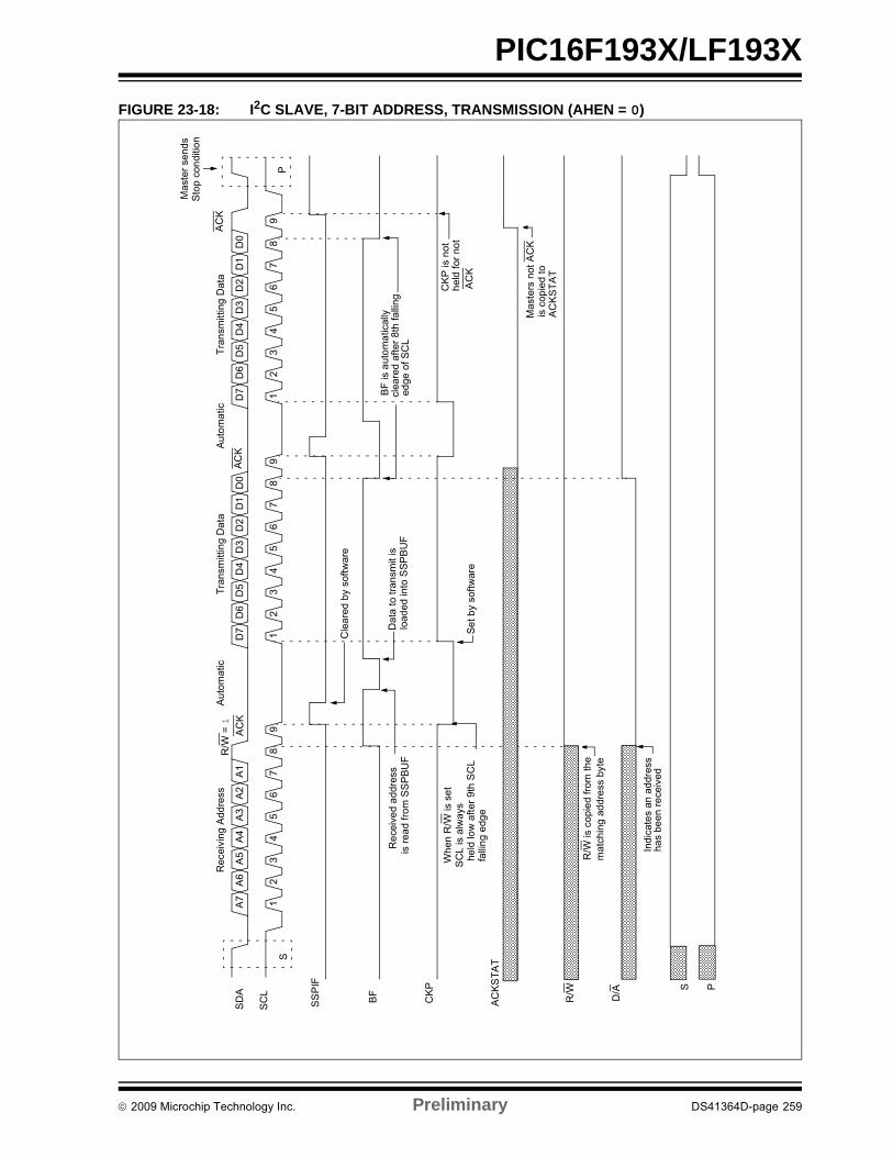
PIC16F193X/LF193X
FIGURE 23-18: I2C SLAVE, 7-BIT ADDRESS, TRANSMISSION (AHEN = 0)
Rec
eivi
ng A
ddre
ssA
uto
mat
icT
rans
mitt
ing
Da
taA
uto
ma
ticT
ran
smitt
ing
Dat
a
A7
A6
A5
A4
A3
A2
A1
D7
D6
D5
D4
D3
D2
D1
D0
D7
D6
D5
D4
D3
D2
D1
D0
12
34
56
78
91
23
45
67
89
12
34
56
78
9
SD
A
SC
L
SS
PIF
BF
CK
P
AC
KS
TA
T
R/W
D/A S P
Re
ceiv
ed
add
ress
Wh
en R
/W is
se
t
R/W
is c
opie
d fr
om th
e
Ind
icat
es
an a
ddr
ess
is r
ead
from
SS
PB
UF
SC
L is
alw
ays
held
low
aft
er 9
th S
CL
falli
ng
edg
e
mat
chin
g a
ddr
ess
byt
e
has
been
re
ceiv
ed
Mas
ters
not
AC
Kis
cop
ied
to
AC
KS
TA
T
CK
P is
not
h
eld
for
not
AC
K
BF
is a
uto
ma
tical
ly
clea
red
aft
er 8
th f
allin
ged
ge o
f S
CL
Dat
a to
tra
nsm
it is
load
ed in
to S
SP
BU
F
Se
t by
soft
war
e
Cle
are
d b
y so
ftw
are
AC
KA
CK
AC
KR
/W=1
SP
Mas
ter
send
sS
top
con
ditio
n
2009 Microchip Technology Inc. Preliminary DS41364D-page 259
PIC16F193X/LF193X
23.5.3.3 7-bit Transmission with Address Hold Enabled
Setting the AHEN bit of the SSPCON3 registerenables additional clock stretching and interruptgeneration after the 8th falling edge of a receivedmatching address. Once a matching address hasbeen clocked in, CKP is cleared and the SSPIFinterrupt is set.
Figure 23-18 displays a standard waveform of a 7-bitAddress Slave Transmission with AHEN enabled.
1. Bus starts Idle.
2. Master sends Start condition; the S bit ofSSPSTAT is set; SSPIF is set if interrupt on Startdetect is enabled.
3. Master sends matching address with R/W bitset. After the 8th falling edge of the SCL line theCKP bit is cleared and SSPIF interrupt is gener-ated.
4. Slave software clears SSPIF.
5. Slave software reads ACKTIM bit of SSPCON3register, and R/W and D/A of the SSPSTAT reg-ister to determine the source of the interrupt.
6. Slave reads the address value from theSSPBUF register clearing the BF bit.
7. Slave software decides from this information if itwishes to ACK or not ACK and sets ACKDT bitof the SSPCON2 register accordingly.
8. Slave sets the CKP bit releasing SCL.
9. Master clocks in the ACK value from the slave.
10. Slave hardware automatically clears the CKP bitand sets SSPIF after the ACK if the R/W bit isset.
11. Slave software clears SSPIF.
12. Slave loads value to transmit to the master intoSSPBUF setting the BF bit.
13. Slave sets CKP bit releasing the clock.
14. Master clocks out the data from the slave andsends an ACK value on the 9th SCL pulse.
15. Slave hardware copies the ACK value into theACKSTAT bit of the SSPCON2 register.
16. Steps 10-15 are repeated for each byte transmit-ted to the master from the slave.
17. If the master sends a not ACK the slavereleases the bus allowing the master to send aStop and end the communication.
Note: SSPBUF cannot be loaded until after theACK.
Note: Master must send a not ACK on the last byteto ensure that the slave releases the SCLline to receive a Stop.
DS41364D-page 260 Preliminary 2009 Microchip Technology Inc.

PIC16F193X/LF193X
FIGURE 23-19: I2C SLAVE, 7-BIT ADDRESS, TRANSMISSION (AHEN = 1)
Rec
eiv
ing
Ad
dres
sA
utom
atic
Tra
nsm
ittin
g D
ata
Aut
oma
ticT
rans
mitt
ing
Da
ta
A7
A6
A5
A4
A3
A2
A1
D7
D6
D5
D4
D3
D2
D1
D0
D7
D6
D5
D4
D3
D2
D1
D0
12
34
56
78
91
23
45
67
89
12
34
56
78
9
SD
A
SC
L
SS
PIF BF
AC
KD
T
AC
KS
TAT
CK
P
R/W D/A
Rec
eiv
ed a
ddr
ess
is r
ead
from
SS
PB
UF
BF
is a
utom
atic
ally
cl
eare
d a
fter
8th
falli
ng
edg
e o
f S
CL
Dat
a to
tra
nsm
it is
loa
ded
into
SS
PB
UF
Cle
ared
by
softw
are
Sla
ve c
lea
rs
AC
KD
T t
o A
CK
addr
ess
Ma
ster
’s A
CK
resp
onse
is c
opie
dto
SS
PS
TAT
CK
P n
ot c
lear
ed
afte
r no
t A
CK
Se
t by
softw
are,
rele
ase
s S
CL
AC
KT
IM is
cle
ared
on
9th
risi
ng e
dge
of S
CL
AC
KT
IM is
set
on
8th
fal
ling
edg
e of
SC
L
Whe
n A
HE
N =
1;
CK
P is
cle
ared
by
har
dwar
eaf
ter
rece
ivin
g m
atch
ing
add
ress
.
Whe
n R
/W =
1;
CK
P is
alw
ays
clea
red
afte
r A
CK
SP
Mas
ter
send
sS
top
cond
ition
AC
KR
/W=1M
ast
er r
ele
ases
SD
Ato
sla
ve f
or A
CK
seq
uen
ce
AC
KA
CK
AC
KT
IM
2009 Microchip Technology Inc. Preliminary DS41364D-page 261
PIC16F193X/LF193X
23.5.4 SLAVE MODE 10-BIT ADDRESS RECEPTION
This section describes a standard sequence of eventsfor the MSSP module configured as an I2C Slave in10-bit Addressing mode.
Figure 23-19 is used as a visual reference for thisdescription.
This is a step by step process of what must be done byslave software to accomplish I2C communication.
1. Bus starts Idle.
2. Master sends Start condition; S bit of SSPSTATis set; SSPIF is set if interrupt on Start detect isenabled.
3. Master sends matching high address with R/Wbit clear; UA bit of the SSPSTAT register is set.
4. Slave sends ACK and SSPIF is set.
5. Software clears the SSPIF bit.
6. Software reads received address from SSPBUFclearing the BF flag.
7. Slave loads low address into SSPADD,releasing SCL.
8. Master sends matching low address byte to theSlave; UA bit is set.
9. Slave sends ACK and SSPIF is set.
10. Slave clears SSPIF.
11. Slave reads the received matching addressfrom SSPBUF clearing BF.
12. Slave loads high address into SSPADD.
13. Master clocks a data byte to the slave andclocks out the slaves ACK on the 9th SCL pulse;SSPIF is set.
14. If SEN bit of SSPCON2 is set, CKP is cleared byhardware and the clock is stretched.
15. Slave clears SSPIF.
16. Slave reads the received byte from SSPBUFclearing BF.
17. If SEN is set the slave sets CKP to release theSCL.
18. Steps 13-17 repeat for each received byte.
19. Master sends Stop to end the transmission.
23.5.5 10-BIT ADDRESSING WITH ADDRESS OR DATA HOLD
Reception using 10-bit addressing with AHEN orDHEN set is the same as with 7-bit modes. The onlydifference is the need to update the SSPADD registerusing the UA bit. All functionality, specifically when theCKP bit is cleared and SCL line is held low are thesame. Figure 23-20 can be used as a reference of aslave in 10-bit addressing with AHEN set.
Figure 23-21 shows a standard waveform for a slavetransmitter in 10-bit Addressing mode.
Note: Updates to the SSPADD register are notallowed until after the ACK sequence.
Note: If the low address does not match, SSPIFand UA are still set so that the slave softwarecan set SSPADD back to the high address.BF is not set because there is no match.CKP is unaffected.
DS41364D-page 262 Preliminary 2009 Microchip Technology Inc.
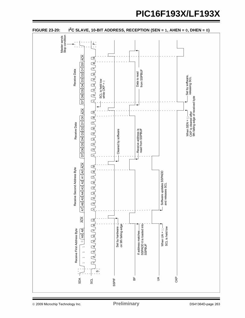
PIC16F193X/LF193X
FIGURE 23-20: I2C SLAVE, 10-BIT ADDRESS, RECEPTION (SEN = 1, AHEN = 0, DHEN = 0)
SS
PIF
Rec
eive
Firs
t Add
ress
Byt
e
AC
K
Rec
eive
Sec
ond
Add
ress
Byt
e AC
K
Rec
eive
Dat
a
AC
K
Rec
eive
Dat
a
AC
K1
11
10
A9
A8
A7
A6
A5
A4
A3
A2
A1
A0
D7
D6
D5
D4
D3
D2
D1
D0
D7
D6
D5
D4
D3
D2
D1
D0
SD
A
SC
L UA
CK
P
12
34
56
78
91
23
45
67
89
12
34
56
78
91
23
45
67
89
P
Mas
ter
send
sS
top
cond
ition
Cle
ared
by
softw
are
Rec
eive
add
ress
is
Sof
twar
e up
date
s S
SP
AD
D
Dat
a is
rea
d
SC
L is
hel
d lo
w
Set
by
softw
are,
whi
le C
KP
= 0
from
SS
PB
UF
rele
asin
g S
CL
Whe
n S
EN
= 1
;C
KP
is c
lear
ed a
fter
9th
falli
ng e
dge
of r
ecei
ved
byte
read
from
SS
PB
UF
and
rele
ases
SC
LW
hen
UA
= 1
;
If ad
dres
s m
atch
es
Set
by
hard
war
eon
9th
falli
ng e
dge
SS
PA
DD
it is
load
ed in
to
SS
PB
UF SC
L is
hel
d lo
w
S
BF
2009 Microchip Technology Inc. Preliminary DS41364D-page 263
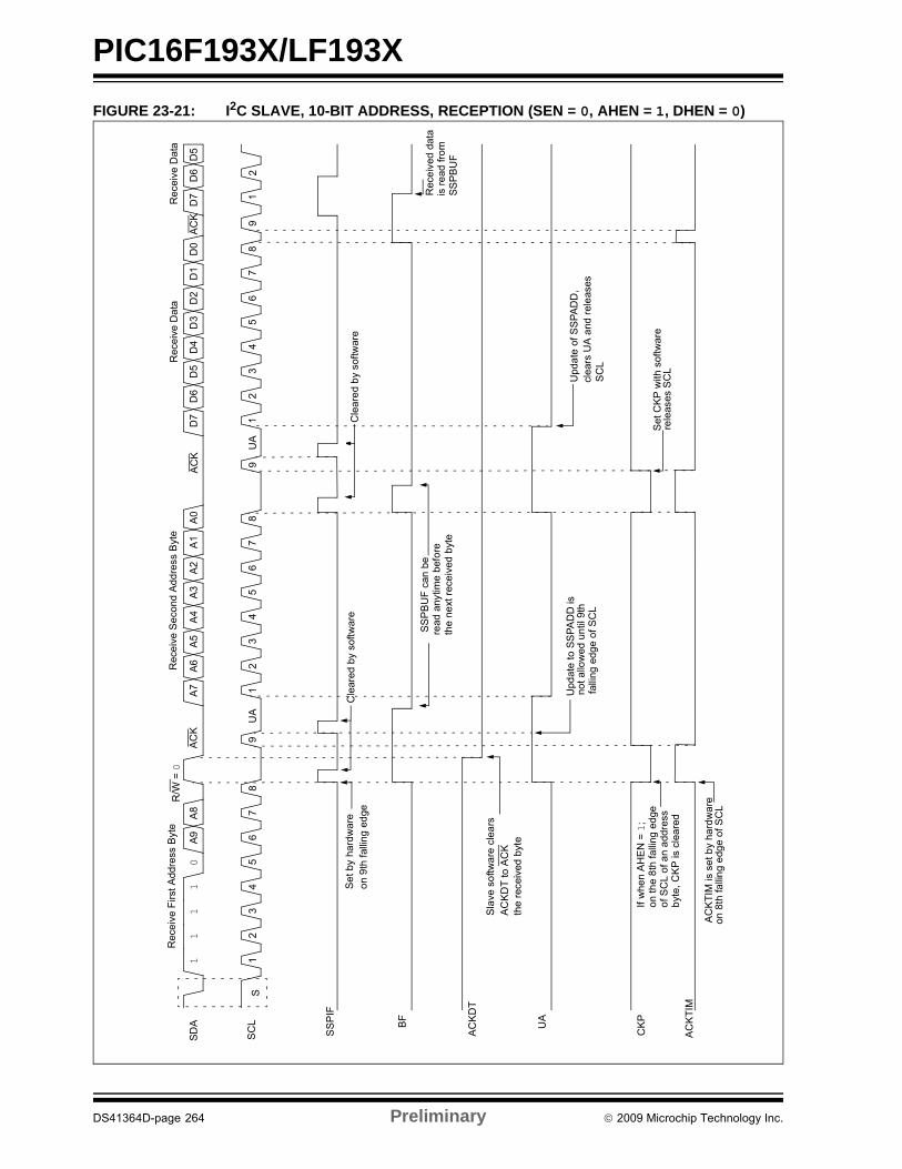
PIC16F193X/LF193X
FIGURE 23-21: I2C SLAVE, 10-BIT ADDRESS, RECEPTION (SEN = 0, AHEN = 1, DHEN = 0)
Rec
eiv
e F
irst
Add
ress
Byt
e
UA
Rec
eiv
e S
eco
nd A
ddre
ss B
yte
UA
Rec
eiv
e D
ata
AC
K
Rec
eive
Dat
a
11
11
0A
9A
8A
7A
6A
5A
4A
3A
2A
1A
0D
7D
6D
5D
4D
3D
2D
1D
0D
7D
6D
5S
DA
SC
L
SS
PIF
BF
AC
KD
T
UA
CK
P
AC
KT
IM
12
34
56
78
9S
AC
KA
CK
12
34
56
78
91
23
45
67
89
12
SS
PB
UF
is r
ead
fro
m
Rec
eiv
ed d
ata
SS
PB
UF
can
be
read
any
time
bef
ore
the
ne
xt r
ece
ived
byt
e
Cle
ared
by
softw
are
falli
ng e
dge
of S
CL
not a
llow
ed u
ntil
9th
Upd
ate
to S
SP
AD
D is
Set
CK
P w
ith s
oftw
are
rele
ases
SC
L
SC
Lcl
ears
UA
and
rel
eas
esU
pda
te o
f SS
PA
DD
,
Se
t by
hard
wa
reo
n 9
th f
allin
g e
dge
Sla
ve s
oftw
are
cle
ars
AC
KD
T to
AC
Kth
e re
ceiv
ed b
yte
If w
hen
AH
EN
=1
;o
n th
e 8
th f
allin
g e
dge
of S
CL
of a
n a
ddre
ssb
yte,
CK
P is
cle
are
d
AC
KT
IM is
se
t by
hard
wa
reon
8th
falli
ng
edg
e of
SC
L
Cle
are
d b
y so
ftwar
e
R/W
= 0
DS41364D-page 264 Preliminary 2009 Microchip Technology Inc.
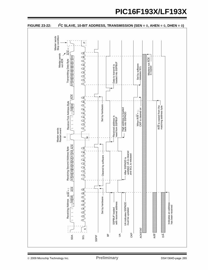
PIC16F193X/LF193X
FIGURE 23-22: I2C SLAVE, 10-BIT ADDRESS, TRANSMISSION (SEN = 0, AHEN = 0, DHEN = 0)
Rec
eivi
ng A
ddre
ss
AC
K
Rec
eiv
ing
Sec
ond
Ad
dre
ss B
yte
Sr
Re
ceiv
e F
irst
Add
ress
Byt
e
AC
K
Tra
nsm
ittin
g D
ata
Byt
e
11
11
0A
9A
8A
7A
6A
5A
4A
3A
2A
1A
01
11
10
A9
A8
D7
D6
D5
D4
D3
D2
D1
D0
SD
A
SC
L
SS
PIF B
F
UA
CK
P
R/W D/A
12
34
56
78
91
23
45
67
89
12
34
56
78
91
23
45
67
89AC
K =
1
P
Ma
ster
sen
ds
Sto
p c
ondi
tion
Ma
ste
r se
nds
not A
CK
Mas
ter
send
s R
esta
rt e
vent
AC
K
R/W
= 0
S
Cle
are
d b
y so
ftwar
e
Afte
r S
SP
AD
D is
upd
ate
d, U
A is
cle
ared
and
SC
L is
rel
eas
ed
Hig
h a
ddr
ess
is lo
ade
d
Rec
eive
d a
ddre
ss is
Dat
a to
tran
smit
is
Se
t by
softw
are
Indi
cate
s a
n a
ddre
ss
Whe
n R
/W =
1;
R/W
is c
opie
d fr
om th
e
Se
t by
hard
wa
re
UA
ind
icat
es
SS
PA
DD
SS
PB
UF
loa
ded
with
rec
eiv
ed a
ddr
ess
mus
t be
upd
ate
d
has
bee
n r
ece
ive
d
loa
ded
into
SS
PB
UF
rele
ase
s S
CL
Ma
ste
rs n
ot A
CK
is c
opi
ed
ma
tchi
ng
add
ress
byt
e
CK
P is
cle
are
d o
n9t
h fa
lling
ed
ge o
f SC
L
rea
d fr
om S
SP
BU
F
back
into
SS
PA
DD
AC
KS
TAT
Set
by
hard
wa
re
2009 Microchip Technology Inc. Preliminary DS41364D-page 265
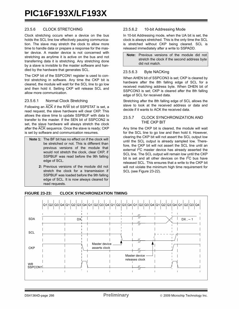
PIC16F193X/LF193X
23.5.6 CLOCK STRETCHING
Clock stretching occurs when a device on the busholds the SCL line low effectively pausing communica-tion. The slave may stretch the clock to allow moretime to handle data or prepare a response for the mas-ter device. A master device is not concerned withstretching as anytime it is active on the bus and nottransferring data it is stretching. Any stretching doneby a slave is invisible to the master software and han-dled by the hardware that generates SCL.
The CKP bit of the SSPCON1 register is used to con-trol stretching in software. Any time the CKP bit iscleared, the module will wait for the SCL line to go lowand then hold it. Setting CKP will release SCL andallow more communication.
23.5.6.1 Normal Clock Stretching
Following an ACK if the R/W bit of SSPSTAT is set, aread request, the slave hardware will clear CKP. Thisallows the slave time to update SSPBUF with data totransfer to the master. If the SEN bit of SSPCON2 isset, the slave hardware will always stretch the clockafter the ACK sequence. Once the slave is ready; CKPis set by software and communication resumes.
23.5.6.2 10-bit Addressing Mode
In 10-bit Addressing mode, when the UA bit is set, theclock is always stretched. This is the only time the SCLis stretched without CKP being cleared. SCL isreleased immediately after a write to SSPADD.
23.5.6.3 Byte NACKing
When AHEN bit of SSPCON3 is set; CKP is cleared byhardware after the 8th falling edge of SCL for areceived matching address byte. When DHEN bit ofSSPCON3 is set; CKP is cleared after the 8th fallingedge of SCL for received data.
Stretching after the 8th falling edge of SCL allows theslave to look at the received address or data anddecide if it wants to ACK the received data.
23.5.7 CLOCK SYNCHRONIZATION AND THE CKP BIT
Any time the CKP bit is cleared, the module will waitfor the SCL line to go low and then hold it. However,clearing the CKP bit will not assert the SCL output lowuntil the SCL output is already sampled low. There-fore, the CKP bit will not assert the SCL line until anexternal I2C master device has already asserted theSCL line. The SCL output will remain low until the CKPbit is set and all other devices on the I2C bus havereleased SCL. This ensures that a write to the CKP bitwill not violate the minimum high time requirement forSCL (see Figure 23-22).
FIGURE 23-23: CLOCK SYNCHRONIZATION TIMING
Note 1: The BF bit has no effect on if the clock willbe stretched or not. This is different thanprevious versions of the module thatwould not stretch the clock, clear CKP, ifSSPBUF was read before the 9th fallingedge of SCL.
2: Previous versions of the module did notstretch the clock for a transmission ifSSPBUF was loaded before the 9th fallingedge of SCL. It is now always cleared forread requests.
Note: Previous versions of the module did notstretch the clock if the second address bytedid not match.
SDA
SCL
DX ‚ – 1DX
WR
Q1 Q2 Q3 Q4 Q1 Q2 Q3 Q4 Q1 Q2 Q3 Q4 Q1 Q2 Q3 Q4 Q1 Q2 Q3 Q4 Q1 Q2 Q3 Q4 Q1 Q2 Q3 Q4
SSPCON1
CKP
Master devicereleases clock
Master deviceasserts clock
DS41364D-page 266 Preliminary 2009 Microchip Technology Inc.
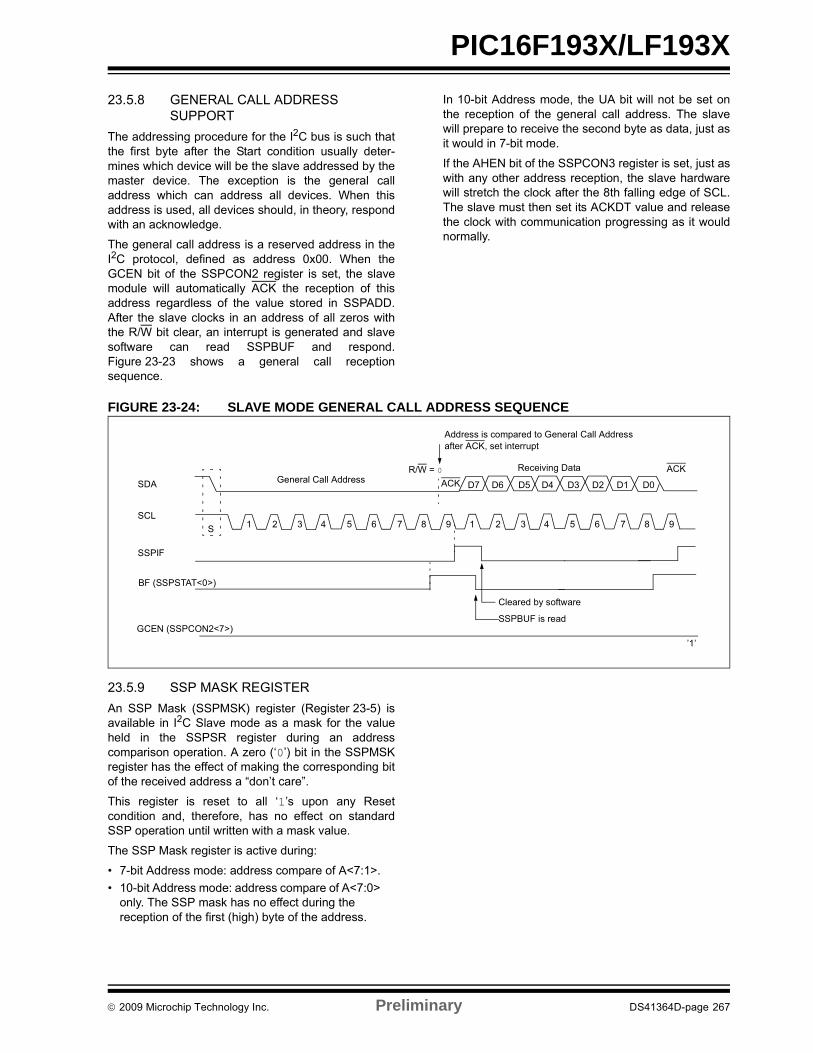
PIC16F193X/LF193X
23.5.8 GENERAL CALL ADDRESS SUPPORT
The addressing procedure for the I2C bus is such thatthe first byte after the Start condition usually deter-mines which device will be the slave addressed by themaster device. The exception is the general calladdress which can address all devices. When thisaddress is used, all devices should, in theory, respondwith an acknowledge.
The general call address is a reserved address in theI2C protocol, defined as address 0x00. When theGCEN bit of the SSPCON2 register is set, the slavemodule will automatically ACK the reception of thisaddress regardless of the value stored in SSPADD.After the slave clocks in an address of all zeros withthe R/W bit clear, an interrupt is generated and slavesoftware can read SSPBUF and respond.Figure 23-23 shows a general call receptionsequence.
In 10-bit Address mode, the UA bit will not be set onthe reception of the general call address. The slavewill prepare to receive the second byte as data, just asit would in 7-bit mode.
If the AHEN bit of the SSPCON3 register is set, just aswith any other address reception, the slave hardwarewill stretch the clock after the 8th falling edge of SCL.The slave must then set its ACKDT value and releasethe clock with communication progressing as it wouldnormally.
FIGURE 23-24: SLAVE MODE GENERAL CALL ADDRESS SEQUENCE
23.5.9 SSP MASK REGISTER
An SSP Mask (SSPMSK) register (Register 23-5) isavailable in I2C Slave mode as a mask for the valueheld in the SSPSR register during an addresscomparison operation. A zero (‘0’) bit in the SSPMSKregister has the effect of making the corresponding bitof the received address a “don’t care”.
This register is reset to all ‘1’s upon any Resetcondition and, therefore, has no effect on standardSSP operation until written with a mask value.
The SSP Mask register is active during:
• 7-bit Address mode: address compare of A<7:1>.
• 10-bit Address mode: address compare of A<7:0> only. The SSP mask has no effect during the reception of the first (high) byte of the address.
SDA
SCL
S
SSPIF
BF (SSPSTAT<0>)
Cleared by software
SSPBUF is read
R/W = 0
ACKGeneral Call Address
Address is compared to General Call Address
Receiving Data ACK
1 2 3 4 5 6 7 8 9 1 2 3 4 5 6 7 8 9
D7 D6 D5 D4 D3 D2 D1 D0
after ACK, set interrupt
GCEN (SSPCON2<7>)
’1’
2009 Microchip Technology Inc. Preliminary DS41364D-page 267
PIC16F193X/LF193X
23.6 I2C Master Mode
Master mode is enabled by setting and clearing theappropriate SSPM bits in the SSPCON1 register andby setting the SSPEN bit. In Master mode, the SCL andSDA lines are set as inputs and are manipulated by theMSSP hardware.
Master mode of operation is supported by interruptgeneration on the detection of the Start and Stop con-ditions. The Stop (P) and Start (S) bits are cleared froma Reset or when the MSSP module is disabled. Controlof the I2C bus may be taken when the P bit is set, or thebus is Idle.
In Firmware Controlled Master mode, user codeconducts all I2C bus operations based on Start andStop bit condition detection. Start and Stop conditiondetection is the only active circuitry in this mode. Allother communication is done by the user softwaredirectly manipulating the SDA and SCL lines.
The following events will cause the SSP Interrupt Flagbit, SSPIF, to be set (SSP interrupt, if enabled):
• Start condition detected
• Stop condition detected
• Data transfer byte transmitted/received
• Acknowledge transmitted/received
• Repeated Start generated
23.6.1 I2C MASTER MODE OPERATION
The master device generates all of the serial clockpulses and the Start and Stop conditions. A transfer isended with a Stop condition or with a Repeated Startcondition. Since the Repeated Start condition is alsothe beginning of the next serial transfer, the I2C bus willnot be released.
In Master Transmitter mode, serial data is outputthrough SDA, while SCL outputs the serial clock. Thefirst byte transmitted contains the slave address of thereceiving device (7 bits) and the Read/Write (R/W) bit.In this case, the R/W bit will be logic ‘0’. Serial data istransmitted 8 bits at a time. After each byte is transmit-ted, an Acknowledge bit is received. Start and Stopconditions are output to indicate the beginning and theend of a serial transfer.
In Master Receive mode, the first byte transmitted con-tains the slave address of the transmitting device(7 bits) and the R/W bit. In this case, the R/W bit will belogic ‘1’. Thus, the first byte transmitted is a 7-bit slaveaddress followed by a ‘1’ to indicate the receive bit.Serial data is received via SDA, while SCL outputs theserial clock. Serial data is received 8 bits at a time. Aftereach byte is received, an Acknowledge bit is transmit-ted. Start and Stop conditions indicate the beginningand end of transmission.
A Baud Rate Generator is used to set the clock fre-quency output on SCL. See Section 23.7 “Baud RateGenerator” for more detail.
Note 1: The MSSP module, when configured inI2C Master mode, does not allow queue-ing of events. For instance, the user is notallowed to initiate a Start condition andimmediately write the SSPBUF register toinitiate transmission before the Start con-dition is complete. In this case, theSSPBUF will not be written to and theWCOL bit will be set, indicating that a writeto the SSPBUF did not occur
2: When in Master mode, Start/Stop detec-tion is masked and an interrupt is gener-ated when the SEN/PEN bit is cleared andthe generation is complete.
DS41364D-page 268 Preliminary 2009 Microchip Technology Inc.

PIC16F193X/LF193X
23.6.2 CLOCK ARBITRATION
Clock arbitration occurs when the master, during anyreceive, transmit or Repeated Start/Stop condition,releases the SCL pin (SCL allowed to float high). Whenthe SCL pin is allowed to float high, the Baud Rate Gen-erator (BRG) is suspended from counting until the SCLpin is actually sampled high. When the SCL pin is sam-pled high, the Baud Rate Generator is reloaded withthe contents of SSPADD<7:0> and begins counting.This ensures that the SCL high time will always be atleast one BRG rollover count in the event that the clockis held low by an external device (Figure 23-25).
FIGURE 23-25: BAUD RATE GENERATOR TIMING WITH CLOCK ARBITRATION
23.6.3 WCOL STATUS FLAG
If the user writes the SSPBUF when a Start, Restart,Stop, Receive or Transmit sequence is in progress, theWCOL is set and the contents of the buffer areunchanged (the write doesn’t occur). Any time theWCOL bit is set it indicates that an action on SSPBUFwas attempted while the module was not idle.
SDA
SCL
SCL deasserted but slave holds
DX ‚ – 1DX
BRG
SCL is sampled high, reload takesplace and BRG starts its count
03h 02h 01h 00h (hold off) 03h 02h
Reload
BRGValue
SCL low (clock arbitration)SCL allowed to transition high
BRG decrements onQ2 and Q4 cycles
Note: Because queueing of events is notallowed, writing to the lower 5 bits ofSSPCON2 is disabled until the Startcondition is complete.
2009 Microchip Technology Inc. Preliminary DS41364D-page 269
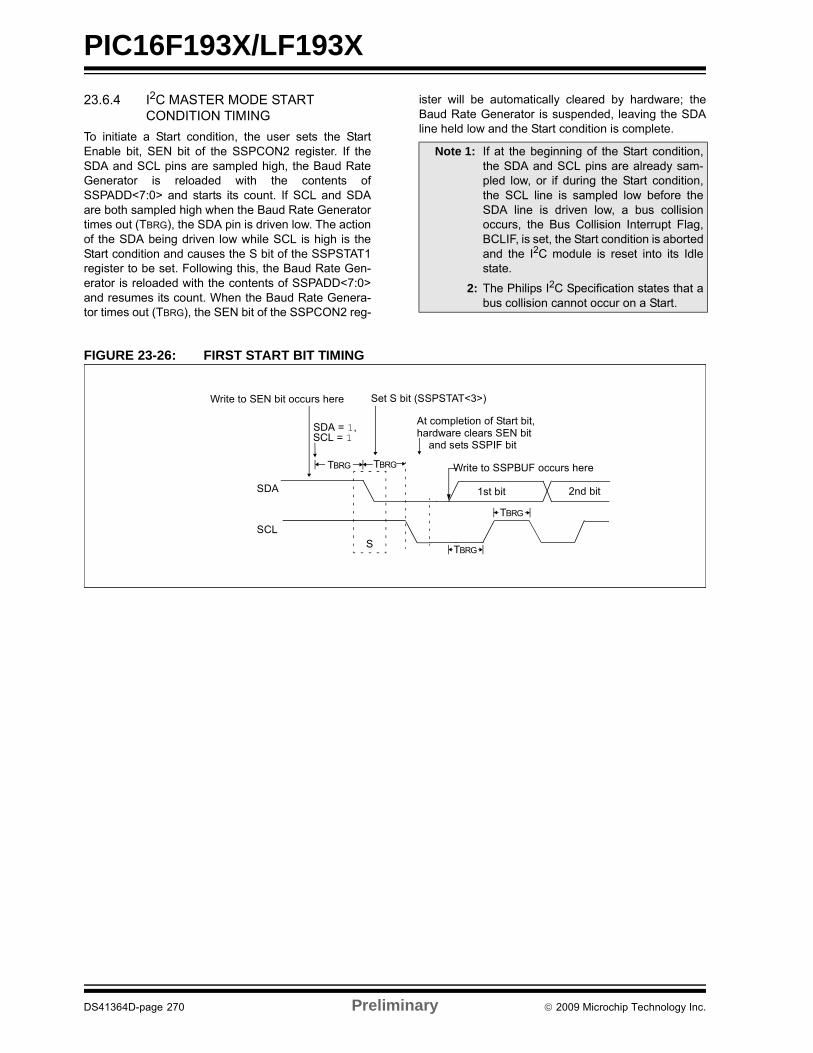
PIC16F193X/LF193X
23.6.4 I2C MASTER MODE START CONDITION TIMING
To initiate a Start condition, the user sets the StartEnable bit, SEN bit of the SSPCON2 register. If theSDA and SCL pins are sampled high, the Baud RateGenerator is reloaded with the contents ofSSPADD<7:0> and starts its count. If SCL and SDAare both sampled high when the Baud Rate Generatortimes out (TBRG), the SDA pin is driven low. The actionof the SDA being driven low while SCL is high is theStart condition and causes the S bit of the SSPSTAT1register to be set. Following this, the Baud Rate Gen-erator is reloaded with the contents of SSPADD<7:0>and resumes its count. When the Baud Rate Genera-tor times out (TBRG), the SEN bit of the SSPCON2 reg-
ister will be automatically cleared by hardware; theBaud Rate Generator is suspended, leaving the SDAline held low and the Start condition is complete.
FIGURE 23-26: FIRST START BIT TIMING
Note 1: If at the beginning of the Start condition,the SDA and SCL pins are already sam-pled low, or if during the Start condition,the SCL line is sampled low before theSDA line is driven low, a bus collisionoccurs, the Bus Collision Interrupt Flag,BCLIF, is set, the Start condition is abortedand the I2C module is reset into its Idlestate.
2: The Philips I2C Specification states that abus collision cannot occur on a Start.
SDA
SCLS
TBRG
1st bit 2nd bit
TBRG
SDA = 1, At completion of Start bit,
SCL = 1
Write to SSPBUF occurs hereTBRG
hardware clears SEN bit
TBRG
Write to SEN bit occurs here Set S bit (SSPSTAT<3>)
and sets SSPIF bit
DS41364D-page 270 Preliminary 2009 Microchip Technology Inc.
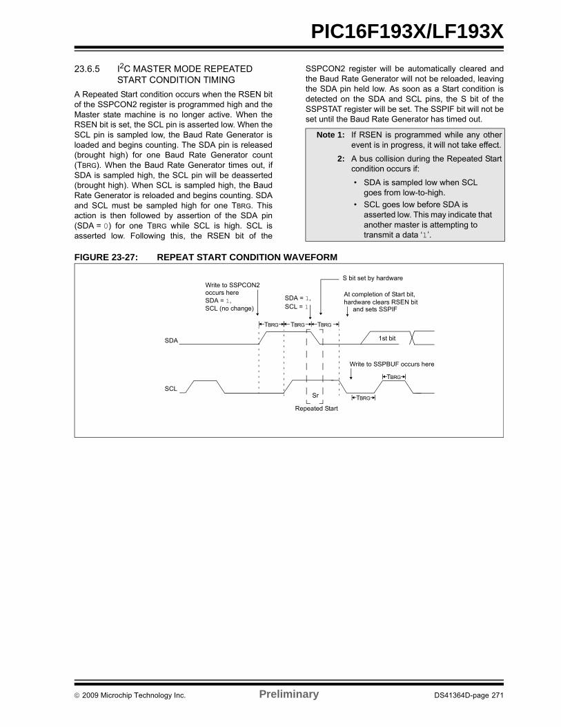
PIC16F193X/LF193X
23.6.5 I2C MASTER MODE REPEATED START CONDITION TIMING
A Repeated Start condition occurs when the RSEN bitof the SSPCON2 register is programmed high and theMaster state machine is no longer active. When theRSEN bit is set, the SCL pin is asserted low. When theSCL pin is sampled low, the Baud Rate Generator isloaded and begins counting. The SDA pin is released(brought high) for one Baud Rate Generator count(TBRG). When the Baud Rate Generator times out, ifSDA is sampled high, the SCL pin will be deasserted(brought high). When SCL is sampled high, the BaudRate Generator is reloaded and begins counting. SDAand SCL must be sampled high for one TBRG. Thisaction is then followed by assertion of the SDA pin(SDA = 0) for one TBRG while SCL is high. SCL isasserted low. Following this, the RSEN bit of the
SSPCON2 register will be automatically cleared andthe Baud Rate Generator will not be reloaded, leavingthe SDA pin held low. As soon as a Start condition isdetected on the SDA and SCL pins, the S bit of theSSPSTAT register will be set. The SSPIF bit will not beset until the Baud Rate Generator has timed out.
FIGURE 23-27: REPEAT START CONDITION WAVEFORM
Note 1: If RSEN is programmed while any otherevent is in progress, it will not take effect.
2: A bus collision during the Repeated Startcondition occurs if:
• SDA is sampled low when SCL goes from low-to-high.
• SCL goes low before SDA is asserted low. This may indicate that another master is attempting to transmit a data ‘1’.
SDA
SCL
Repeated Start
Write to SSPCON2
Write to SSPBUF occurs here
At completion of Start bit, hardware clears RSEN bit
1st bit
S bit set by hardware
TBRG
TBRG
SDA = 1, SDA = 1,
SCL (no change) SCL = 1
occurs here
TBRG TBRG TBRG
and sets SSPIF
Sr
2009 Microchip Technology Inc. Preliminary DS41364D-page 271

PIC16F193X/LF193X
23.6.6 I2C MASTER MODE TRANSMISSION
Transmission of a data byte, a 7-bit address or theother half of a 10-bit address is accomplished by simplywriting a value to the SSPBUF register. This action willset the Buffer Full flag bit, BF, and allow the Baud RateGenerator to begin counting and start the next trans-mission. Each bit of address/data will be shifted outonto the SDA pin after the falling edge of SCL isasserted. SCL is held low for one Baud Rate Generatorrollover count (TBRG). Data should be valid before SCLis released high. When the SCL pin is released high, itis held that way for TBRG. The data on the SDA pinmust remain stable for that duration and some holdtime after the next falling edge of SCL. After the eighthbit is shifted out (the falling edge of the eighth clock),the BF flag is cleared and the master releases SDA.This allows the slave device being addressed torespond with an ACK bit during the ninth bit time if anaddress match occurred, or if data was received prop-erly. The status of ACK is written into the ACKSTAT biton the rising edge of the ninth clock. If the masterreceives an Acknowledge, the Acknowledge Status bit,ACKSTAT, is cleared. If not, the bit is set. After the ninthclock, the SSPIF bit is set and the master clock (BaudRate Generator) is suspended until the next data byteis loaded into the SSPBUF, leaving SCL low and SDAunchanged (Figure 23-27).
After the write to the SSPBUF, each bit of the addresswill be shifted out on the falling edge of SCL until allseven address bits and the R/W bit are completed. Onthe falling edge of the eighth clock, the master willrelease the SDA pin, allowing the slave to respond withan Acknowledge. On the falling edge of the ninth clock,the master will sample the SDA pin to see if the addresswas recognized by a slave. The status of the ACK bit isloaded into the ACKSTAT Status bit of the SSPCON2register. Following the falling edge of the ninth clocktransmission of the address, the SSPIF is set, the BFflag is cleared and the Baud Rate Generator is turnedoff until another write to the SSPBUF takes place, hold-ing SCL low and allowing SDA to float.
23.6.6.1 BF Status Flag
In Transmit mode, the BF bit of the SSPSTAT registeris set when the CPU writes to SSPBUF and is clearedwhen all 8 bits are shifted out.
23.6.6.2 WCOL Status Flag
If the user writes the SSPBUF when a transmit isalready in progress (i.e., SSPSR is still shifting out adata byte), the WCOL is set and the contents of the buf-fer are unchanged (the write doesn’t occur).
WCOL must be cleared by software before the nexttransmission.
23.6.6.3 ACKSTAT Status Flag
In Transmit mode, the ACKSTAT bit of the SSPCON2register is cleared when the slave has sent an Acknowl-edge (ACK = 0) and is set when the slave does notAcknowledge (ACK = 1). A slave sends an Acknowl-edge when it has recognized its address (including ageneral call), or when the slave has properly receivedits data.
23.6.6.4 Typical transmit sequence:
1. The user generates a Start condition by settingthe SEN bit of the SSPCON2 register.
2. SSPIF is set by hardware on completion of theStart.
3. SSPIF is cleared by software.
4. The MSSP module will wait the required starttime before any other operation takes place.
5. The user loads the SSPBUF with the slaveaddress to transmit.
6. Address is shifted out the SDA pin until all 8 bitsare transmitted. Transmission begins as soonas SSPBUF is written to.
7. The MSSP module shifts in the ACK bit from theslave device and writes its value into theACKSTAT bit of the SSPCON2 register.
8. The MSSP module generates an interrupt at theend of the ninth clock cycle by setting the SSPIFbit.
9. The user loads the SSPBUF with eight bits ofdata.
10. Data is shifted out the SDA pin until all 8 bits aretransmitted.
11. The MSSP module shifts in the ACK bit from theslave device and writes its value into theACKSTAT bit of the SSPCON2 register.
12. Steps 8-11 are repeated for all transmitted databytes.
13. The user generates a Stop or Restart conditionby setting the PEN or RSEN bits of theSSPCON2 register. Interrupt is generated oncethe Stop/Restart condition is complete.
DS41364D-page 272 Preliminary 2009 Microchip Technology Inc.

PIC16F193X/LF193X
FIGURE 23-28: I2C MASTER MODE WAVEFORM (TRANSMISSION, 7 OR 10-BIT ADDRESS)
SD
A
SC
L
SS
PIF
BF
(S
SP
STA
T<
0>
)
SE
N
A7
A6
A5
A4
A3
A2
A1
AC
K =
0D
7D
6D
5D
4D
3D
2D
1D
0
AC
KT
ran
smitt
ing
Dat
a o
r S
eco
nd H
alf
R/W
= 0
Tra
nsm
it A
ddr
ess
to S
lave
12
34
56
78
91
23
45
67
89
P
Cle
are
d b
y so
ftwar
e se
rvic
e r
out
ine
SS
PB
UF
is w
ritte
n by
so
ftwa
re
from
SS
P in
terr
upt
Afte
r S
tart
co
nditi
on,
SE
N c
lear
ed b
y h
ardw
are
S
SS
PB
UF
wri
tten
with
7-b
it a
ddre
ss a
nd R
/Wst
art t
rans
mit
SC
L h
eld
low
whi
le C
PU
resp
ond
s to
SS
PIF
SE
N =
0
of 1
0-b
it A
ddre
ss
Wri
te S
SP
CO
N2
<0>
SE
N =
1S
tart
con
ditio
n b
egin
sF
rom
sla
ve,
clea
r A
CK
STA
T b
it S
SP
CO
N2<
6>
AC
KS
TAT
in
SS
PC
ON
2 =
1
Cle
ared
by
softw
are
SS
PB
UF
writ
ten
PE
N
R/W
Cle
are
d b
y so
ftwar
e
2009 Microchip Technology Inc. Preliminary DS41364D-page 273
PIC16F193X/LF193X
23.6.7 I2C MASTER MODE RECEPTION
Master mode reception is enabled by programming theReceive Enable bit, RCEN bit of the SSPCON2register.
The Baud Rate Generator begins counting and on eachrollover, the state of the SCL pin changes(high-to-low/low-to-high) and data is shifted into theSSPSR. After the falling edge of the eighth clock, thereceive enable flag is automatically cleared, the con-tents of the SSPSR are loaded into the SSPBUF, theBF flag bit is set, the SSPIF flag bit is set and the BaudRate Generator is suspended from counting, holdingSCL low. The MSSP is now in Idle state awaiting thenext command. When the buffer is read by the CPU,the BF flag bit is automatically cleared. The user canthen send an Acknowledge bit at the end of receptionby setting the Acknowledge Sequence Enable, ACKENbit of the SSPCON2 register.
23.6.7.1 BF Status Flag
In receive operation, the BF bit is set when an addressor data byte is loaded into SSPBUF from SSPSR. It iscleared when the SSPBUF register is read.
23.6.7.2 SSPOV Status Flag
In receive operation, the SSPOV bit is set when 8 bitsare received into the SSPSR and the BF flag bit isalready set from a previous reception.
23.6.7.3 WCOL Status Flag
If the user writes the SSPBUF when a receive isalready in progress (i.e., SSPSR is still shifting in a databyte), the WCOL bit is set and the contents of the bufferare unchanged (the write doesn’t occur).
23.6.7.4 Typical Receive Sequence:
1. The user generates a Start condition by settingthe SEN bit of the SSPCON2 register.
2. SSPIF is set by hardware on completion of theStart.
3. SSPIF is cleared by software.
4. User writes SSPBUF with the slave address totransmit and the R/W bit set.
5. Address is shifted out the SDA pin until all 8 bitsare transmitted. Transmission begins as soonas SSPBUF is written to.
6. The MSSP module shifts in the ACK bit from theslave device and writes its value into theACKSTAT bit of the SSPCON2 register.
7. The MSSP module generates an interrupt at theend of the ninth clock cycle by setting the SSPIFbit.
8. User sets the RCEN bit of the SSPCON2 registerand the Master clocks in a byte from the slave.
9. After the 8th falling edge of SCL, SSPIF and BFare set.
10. Master clears SSPIF and reads the receivedbyte from SSPUF, clears BF.
11. Master sets ACK value sent to slave in ACKDTbit of the SSPCON2 register and initiates theACK by setting the ACKEN bit.
12. Masters ACK is clocked out to the Slave andSSPIF is set.
13. User clears SSPIF.
14. Steps 8-13 are repeated for each received bytefrom the slave.
15. Master sends a not ACK or Stop to endcommunication.
Note: The MSSP module must be in an Idle statebefore the RCEN bit is set or the RCEN bitwill be disregarded.
DS41364D-page 274 Preliminary 2009 Microchip Technology Inc.
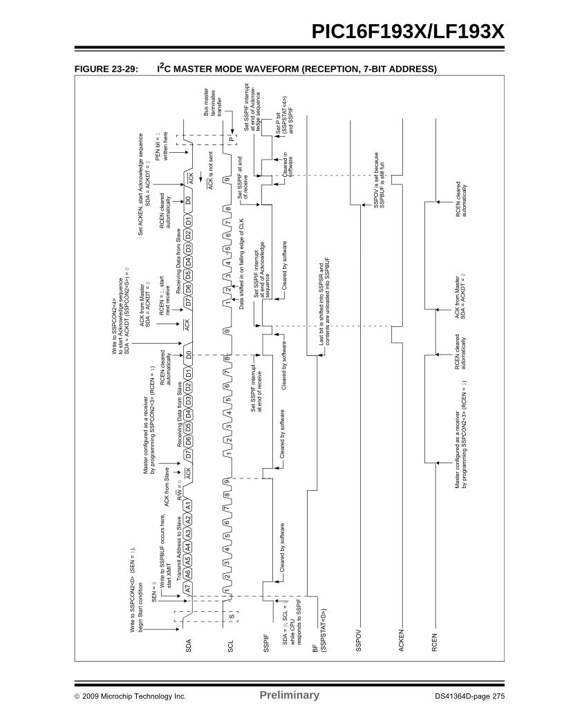
PIC16F193X/LF193X
FIGURE 23-29: I2C MASTER MODE WAVEFORM (RECEPTION, 7-BIT ADDRESS)
P9
87
65
D0
D1
D2
D3
D4
D5
D6
D7
S
A7
A6
A5
A4
A3
A2
A1
SD
A
SC
L1
23
45
67
89
12
34
56
78
91
23
4
Bu
s m
aste
rte
rmin
ate
str
ansf
er
AC
K
Re
ceiv
ing
Dat
a fr
om
Sla
veR
ece
ivin
g D
ata
from
Sla
ve
D0
D1
D2
D3
D4
D5
D6
D7
AC
K
R/W
= 0
Tra
nsm
it A
dd
ress
to
Sla
ve
SS
PIF
BF
AC
K is
no
t se
nt
Wri
te to
SS
PC
ON
2<
0>
(SE
N =
1),
Wri
te to
SS
PB
UF
occ
urs
he
re,
AC
K fr
om
Sla
veMa
ste
r co
nfig
ure
d a
s a
re
ceiv
er
by p
rog
ram
min
g S
SP
CO
N2
<3
> (
RC
EN
= 1
)P
EN
bit
= 1
wri
tten
he
re
Da
ta s
hifte
d in
on
falli
ng
edg
e o
f CL
K
Cle
are
d b
y so
ftwar
e
sta
rt X
MIT
SE
N =
0
SS
PO
V
SD
A =
0,
SC
L =
1w
hile
CP
U
(SS
PS
TAT
<0>
)
AC
K
Cle
are
d b
y so
ftwa
reC
lea
red
by
softw
are
Set
SS
PIF
inte
rru
pt
at
end
of
rece
ive
Se
t P
bit
(SS
PS
TAT
<4
>)
and
SS
PIF
Cle
are
d in
softw
are
AC
K f
rom
Mas
ter
Se
t S
SP
IF a
t e
nd
Se
t S
SP
IF in
terr
upt
at e
nd
of
Ack
no
wle
dg
ese
qu
en
ce
Se
t S
SP
IF in
terr
up
ta
t en
d o
f Ack
now
-le
dg
e se
qu
ence
of r
ece
ive
Se
t A
CK
EN
, st
art
Ack
no
wle
dge
se
que
nce
SS
PO
V is
se
t b
eca
use
SS
PB
UF
is s
till f
ull
SD
A =
AC
KD
T =
1
RC
EN
cle
are
dau
tom
atic
ally
RC
EN
= 1
, st
art
next
re
ceiv
e
Wri
te t
o S
SP
CO
N2
<4
>to
sta
rt A
ckno
wle
dge
sequ
ence
SD
A =
AC
KD
T (
SS
PC
ON
2<
5>
) =
0
RC
EN
cle
are
dau
tom
atic
ally
resp
on
ds
to S
SP
IF
AC
KE
Nbeg
in S
tart
co
nd
itio
n
Cle
are
d b
y so
ftwar
e
SD
A =
AC
KD
T =
0
Last
bit
is s
hifte
d in
to S
SP
SR
and
cont
en
ts a
re u
nlo
ade
d in
to S
SP
BU
F
RC
EN
Ma
ster
co
nfig
ure
d a
s a
re
ceiv
er
by
pro
gra
mm
ing
SS
PC
ON
2<
3>
(R
CE
N =
1)
RC
EN
cle
are
dau
tom
atic
ally
AC
K f
rom
Ma
ste
rS
DA
= A
CK
DT
= 0
R
CE
N c
lea
red
au
tom
atic
ally
2009 Microchip Technology Inc. Preliminary DS41364D-page 275
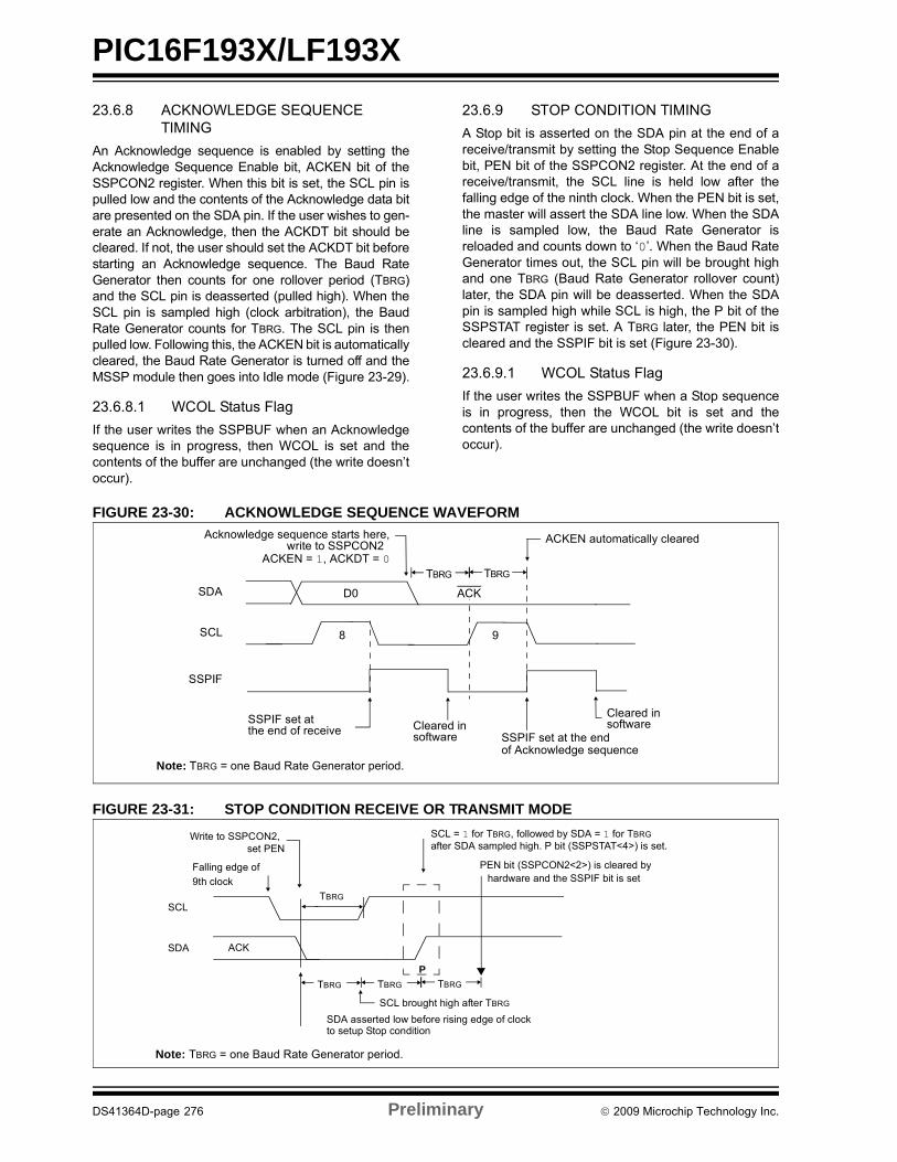
PIC16F193X/LF193X
23.6.8 ACKNOWLEDGE SEQUENCE TIMING
An Acknowledge sequence is enabled by setting theAcknowledge Sequence Enable bit, ACKEN bit of theSSPCON2 register. When this bit is set, the SCL pin ispulled low and the contents of the Acknowledge data bitare presented on the SDA pin. If the user wishes to gen-erate an Acknowledge, then the ACKDT bit should becleared. If not, the user should set the ACKDT bit beforestarting an Acknowledge sequence. The Baud RateGenerator then counts for one rollover period (TBRG)and the SCL pin is deasserted (pulled high). When theSCL pin is sampled high (clock arbitration), the BaudRate Generator counts for TBRG. The SCL pin is thenpulled low. Following this, the ACKEN bit is automaticallycleared, the Baud Rate Generator is turned off and theMSSP module then goes into Idle mode (Figure 23-29).
23.6.8.1 WCOL Status Flag
If the user writes the SSPBUF when an Acknowledgesequence is in progress, then WCOL is set and thecontents of the buffer are unchanged (the write doesn’toccur).
23.6.9 STOP CONDITION TIMING
A Stop bit is asserted on the SDA pin at the end of areceive/transmit by setting the Stop Sequence Enablebit, PEN bit of the SSPCON2 register. At the end of areceive/transmit, the SCL line is held low after thefalling edge of the ninth clock. When the PEN bit is set,the master will assert the SDA line low. When the SDAline is sampled low, the Baud Rate Generator isreloaded and counts down to ‘0’. When the Baud RateGenerator times out, the SCL pin will be brought highand one TBRG (Baud Rate Generator rollover count)later, the SDA pin will be deasserted. When the SDApin is sampled high while SCL is high, the P bit of theSSPSTAT register is set. A TBRG later, the PEN bit iscleared and the SSPIF bit is set (Figure 23-30).
23.6.9.1 WCOL Status Flag
If the user writes the SSPBUF when a Stop sequenceis in progress, then the WCOL bit is set and thecontents of the buffer are unchanged (the write doesn’toccur).
FIGURE 23-30: ACKNOWLEDGE SEQUENCE WAVEFORM
FIGURE 23-31: STOP CONDITION RECEIVE OR TRANSMIT MODE
Note: TBRG = one Baud Rate Generator period.
SDA
SCL
SSPIF set at
Acknowledge sequence starts here,write to SSPCON2
ACKEN automatically cleared
Cleared in
TBRG TBRG
the end of receive
8
ACKEN = 1, ACKDT = 0
D0
9
SSPIF
software SSPIF set at the endof Acknowledge sequence
Cleared insoftware
ACK
SCL
SDA
SDA asserted low before rising edge of clock
Write to SSPCON2,set PEN
Falling edge of
SCL = 1 for TBRG, followed by SDA = 1 for TBRG
9th clock
SCL brought high after TBRG
Note: TBRG = one Baud Rate Generator period.
TBRG TBRG
after SDA sampled high. P bit (SSPSTAT<4>) is set.
TBRG
to setup Stop condition
ACK
P
TBRG
PEN bit (SSPCON2<2>) is cleared by hardware and the SSPIF bit is set
DS41364D-page 276 Preliminary 2009 Microchip Technology Inc.

PIC16F193X/LF193X
23.6.10 SLEEP OPERATION
While in Sleep mode, the I2C slave module can receiveaddresses or data and when an address match orcomplete byte transfer occurs, wake the processorfrom Sleep (if the MSSP interrupt is enabled).
23.6.11 EFFECTS OF A RESET
A Reset disables the MSSP module and terminates thecurrent transfer.
23.6.12 MULTI-MASTER MODE
In Multi-Master mode, the interrupt generation on thedetection of the Start and Stop conditions allows thedetermination of when the bus is free. The Stop (P) andStart (S) bits are cleared from a Reset or when theMSSP module is disabled. Control of the I2C bus maybe taken when the P bit of the SSPSTAT register is set,or the bus is Idle, with both the S and P bits clear. Whenthe bus is busy, enabling the SSP interrupt will gener-ate the interrupt when the Stop condition occurs.
In multi-master operation, the SDA line must bemonitored for arbitration to see if the signal level is theexpected output level. This check is performed byhardware with the result placed in the BCLIF bit.
The states where arbitration can be lost are:
• Address Transfer
• Data Transfer
• A Start Condition
• A Repeated Start Condition
• An Acknowledge Condition
23.6.13 MULTI -MASTER COMMUNICATION, BUS COLLISION AND BUS ARBITRATION
Multi-Master mode support is achieved by bus arbitra-tion. When the master outputs address/data bits ontothe SDA pin, arbitration takes place when the masteroutputs a ‘1’ on SDA, by letting SDA float high andanother master asserts a ‘0’. When the SCL pin floatshigh, data should be stable. If the expected data onSDA is a ‘1’ and the data sampled on the SDA pin is ‘0’,then a bus collision has taken place. The master will setthe Bus Collision Interrupt Flag, BCLIF, and reset theI2C port to its Idle state (Figure 23-31).
If a transmit was in progress when the bus collisionoccurred, the transmission is halted, the BF flag iscleared, the SDA and SCL lines are deasserted and theSSPBUF can be written to. When the user services thebus collision Interrupt Service Routine and if the I2Cbus is free, the user can resume communication byasserting a Start condition.
If a Start, Repeated Start, Stop or Acknowledge condi-tion was in progress when the bus collision occurred, thecondition is aborted, the SDA and SCL lines are deas-serted and the respective control bits in the SSPCON2register are cleared. When the user services the bus col-lision Interrupt Service Routine and if the I2C bus is free,the user can resume communication by asserting a Startcondition.
The master will continue to monitor the SDA and SCLpins. If a Stop condition occurs, the SSPIF bit will be set.
A write to the SSPBUF will start the transmission ofdata at the first data bit, regardless of where thetransmitter left off when the bus collision occurred.
In Multi-Master mode, the interrupt generation on thedetection of Start and Stop conditions allows the deter-mination of when the bus is free. Control of the I2C buscan be taken when the P bit is set in the SSPSTATregister, or the bus is Idle and the S and P bits arecleared.
FIGURE 23-32: BUS COLLISION TIMING FOR TRANSMIT AND ACKNOWLEDGE
SDA
SCL
BCLIF
SDA released
SDA line pulled lowby another source
Sample SDA. While SCL is high,data doesn’t match what is driven
Bus collision has occurred.
Set bus collisioninterrupt (BCLIF)
by the master.
by master
Data changeswhile SCL = 0
2009 Microchip Technology Inc. Preliminary DS41364D-page 277
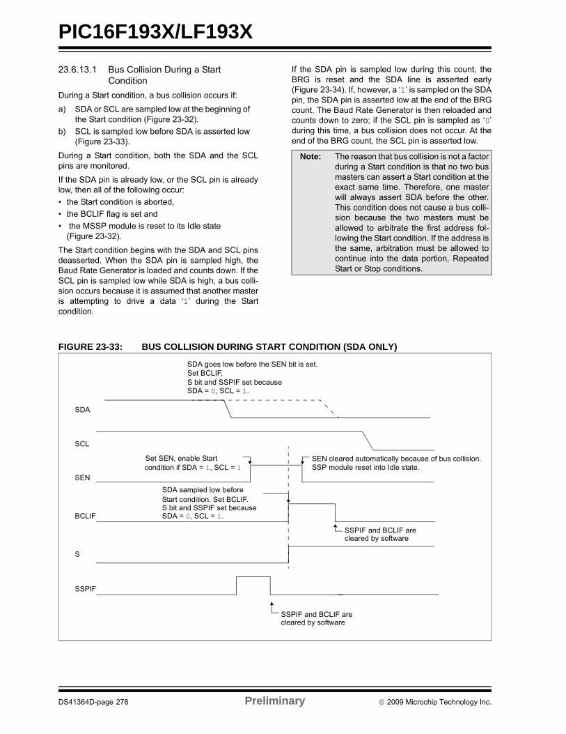
PIC16F193X/LF193X
23.6.13.1 Bus Collision During a Start Condition
During a Start condition, a bus collision occurs if:
a) SDA or SCL are sampled low at the beginning ofthe Start condition (Figure 23-32).
b) SCL is sampled low before SDA is asserted low(Figure 23-33).
During a Start condition, both the SDA and the SCLpins are monitored.
If the SDA pin is already low, or the SCL pin is alreadylow, then all of the following occur:
• the Start condition is aborted,
• the BCLIF flag is set and
• the MSSP module is reset to its Idle state (Figure 23-32).
The Start condition begins with the SDA and SCL pinsdeasserted. When the SDA pin is sampled high, theBaud Rate Generator is loaded and counts down. If theSCL pin is sampled low while SDA is high, a bus colli-sion occurs because it is assumed that another masteris attempting to drive a data ‘1’ during the Startcondition.
If the SDA pin is sampled low during this count, theBRG is reset and the SDA line is asserted early(Figure 23-34). If, however, a ‘1’ is sampled on the SDApin, the SDA pin is asserted low at the end of the BRGcount. The Baud Rate Generator is then reloaded andcounts down to zero; if the SCL pin is sampled as ‘0’during this time, a bus collision does not occur. At theend of the BRG count, the SCL pin is asserted low.
FIGURE 23-33: BUS COLLISION DURING START CONDITION (SDA ONLY)
Note: The reason that bus collision is not a factorduring a Start condition is that no two busmasters can assert a Start condition at theexact same time. Therefore, one masterwill always assert SDA before the other.This condition does not cause a bus colli-sion because the two masters must beallowed to arbitrate the first address fol-lowing the Start condition. If the address isthe same, arbitration must be allowed tocontinue into the data portion, RepeatedStart or Stop conditions.
SDA
SCL
SEN
SDA sampled low before
SDA goes low before the SEN bit is set.
S bit and SSPIF set because
SSP module reset into Idle state.SEN cleared automatically because of bus collision.
S bit and SSPIF set because
Set SEN, enable Startcondition if SDA = 1, SCL = 1
SDA = 0, SCL = 1.
BCLIF
S
SSPIF
SDA = 0, SCL = 1.
SSPIF and BCLIF arecleared by software
SSPIF and BCLIF arecleared by software
Set BCLIF,
Start condition. Set BCLIF.
DS41364D-page 278 Preliminary 2009 Microchip Technology Inc.

PIC16F193X/LF193X
FIGURE 23-34: BUS COLLISION DURING START CONDITION (SCL = 0)
FIGURE 23-35: BRG RESET DUE TO SDA ARBITRATION DURING START CONDITION
SDA
SCL
SENbus collision occurs. Set BCLIF.SCL = 0 before SDA = 0,
Set SEN, enable Startsequence if SDA = 1, SCL = 1
TBRG TBRG
SDA = 0, SCL = 1
BCLIF
S
SSPIF
Interrupt clearedby software
bus collision occurs. Set BCLIF.SCL = 0 before BRG time-out,
’0’ ’0’
’0’’0’
SDA
SCL
SEN
Set SLess than TBRG
TBRG
SDA = 0, SCL = 1
BCLIF
S
SSPIF
S
Interrupts clearedby softwareset SSPIF
SDA = 0, SCL = 1,
SCL pulled low after BRGtime-out
Set SSPIF
’0’
SDA pulled low by other master.Reset BRG and assert SDA.
Set SEN, enable Startsequence if SDA = 1, SCL = 1
2009 Microchip Technology Inc. Preliminary DS41364D-page 279
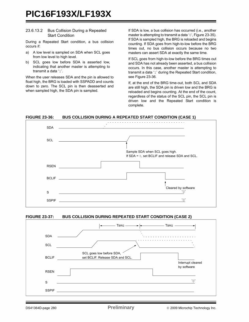
PIC16F193X/LF193X
23.6.13.2 Bus Collision During a Repeated Start Condition
During a Repeated Start condition, a bus collisionoccurs if:
a) A low level is sampled on SDA when SCL goesfrom low level to high level.
b) SCL goes low before SDA is asserted low,indicating that another master is attempting totransmit a data ‘1’.
When the user releases SDA and the pin is allowed tofloat high, the BRG is loaded with SSPADD and countsdown to zero. The SCL pin is then deasserted andwhen sampled high, the SDA pin is sampled.
If SDA is low, a bus collision has occurred (i.e., anothermaster is attempting to transmit a data ‘0’, Figure 23-35).If SDA is sampled high, the BRG is reloaded and beginscounting. If SDA goes from high-to-low before the BRGtimes out, no bus collision occurs because no twomasters can assert SDA at exactly the same time.
If SCL goes from high-to-low before the BRG times outand SDA has not already been asserted, a bus collisionoccurs. In this case, another master is attempting totransmit a data ‘1’ during the Repeated Start condition,see Figure 23-36.
If, at the end of the BRG time-out, both SCL and SDAare still high, the SDA pin is driven low and the BRG isreloaded and begins counting. At the end of the count,regardless of the status of the SCL pin, the SCL pin isdriven low and the Repeated Start condition iscomplete.
FIGURE 23-36: BUS COLLISION DURING A REPEATED START CONDITION (CASE 1)
FIGURE 23-37: BUS COLLISION DURING REPEATED START CONDITION (CASE 2)
SDA
SCL
RSEN
BCLIF
S
SSPIF
Sample SDA when SCL goes high.If SDA = 0, set BCLIF and release SDA and SCL.
Cleared by software
’0’
’0’
SDA
SCL
BCLIF
RSEN
S
SSPIF
Interrupt clearedby software
SCL goes low before SDA,set BCLIF. Release SDA and SCL.
TBRG TBRG
’0’
DS41364D-page 280 Preliminary 2009 Microchip Technology Inc.

PIC16F193X/LF193X
23.6.13.3 Bus Collision During a Stop Condition
Bus collision occurs during a Stop condition if:
a) After the SDA pin has been deasserted andallowed to float high, SDA is sampled low afterthe BRG has timed out.
b) After the SCL pin is deasserted, SCL is sampledlow before SDA goes high.
The Stop condition begins with SDA asserted low.When SDA is sampled low, the SCL pin is allowed tofloat. When the pin is sampled high (clock arbitration),the Baud Rate Generator is loaded with SSPADD andcounts down to 0. After the BRG times out, SDA issampled. If SDA is sampled low, a bus collision hasoccurred. This is due to another master attempting todrive a data ‘0’ (Figure 23-37). If the SCL pin is sampledlow before SDA is allowed to float high, a bus collisionoccurs. This is another case of another masterattempting to drive a data ‘0’ (Figure 23-38).
FIGURE 23-38: BUS COLLISION DURING A STOP CONDITION (CASE 1)
FIGURE 23-39: BUS COLLISION DURING A STOP CONDITION (CASE 2)
SDA
SCL
BCLIF
PEN
P
SSPIF
TBRG TBRG TBRG
SDA asserted low
SDA sampledlow after TBRG,set BCLIF
’0’
’0’
SDA
SCL
BCLIF
PEN
P
SSPIF
TBRG TBRG TBRG
Assert SDA SCL goes low before SDA goes high,set BCLIF
’0’
’0’
2009 Microchip Technology Inc. Preliminary DS41364D-page 281
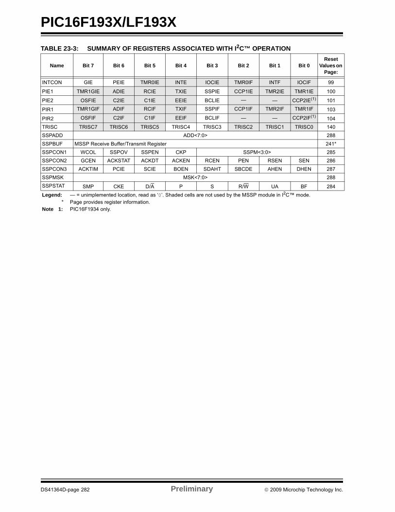
PIC16F193X/LF193X
TABLE 23-3: SUMMARY OF REGISTERS ASSOCIATED WITH I2C™ OPERATION
Name Bit 7 Bit 6 Bit 5 Bit 4 Bit 3 Bit 2 Bit 1 Bit 0Reset
Values on Page:
INTCON GIE PEIE TMR0IE INTE IOCIE TMR0IF INTF IOCIF 99
PIE1 TMR1GIE ADIE RCIE TXIE SSPIE CCP1IE TMR2IE TMR1IE 100
PIE2 OSFIE C2IE C1IE EEIE BCLIE — — CCP2IE(1) 101
PIR1 TMR1GIF ADIF RCIF TXIF SSPIF CCP1IF TMR2IF TMR1IF 103
PIR2 OSFIF C2IF C1IF EEIF BCLIF — — CCP2IF(1) 104
TRISC TRISC7 TRISC6 TRISC5 TRISC4 TRISC3 TRISC2 TRISC1 TRISC0 140
SSPADD ADD<7:0> 288
SSPBUF MSSP Receive Buffer/Transmit Register 241*
SSPCON1 WCOL SSPOV SSPEN CKP SSPM<3:0> 285
SSPCON2 GCEN ACKSTAT ACKDT ACKEN RCEN PEN RSEN SEN 286
SSPCON3 ACKTIM PCIE SCIE BOEN SDAHT SBCDE AHEN DHEN 287
SSPMSK MSK<7:0> 288
SSPSTAT SMP CKE D/A P S R/W UA BF 284
Legend: — = unimplemented location, read as ‘0’. Shaded cells are not used by the MSSP module in I2C™ mode.* Page provides register information.
Note 1: PIC16F1934 only.
DS41364D-page 282 Preliminary 2009 Microchip Technology Inc.
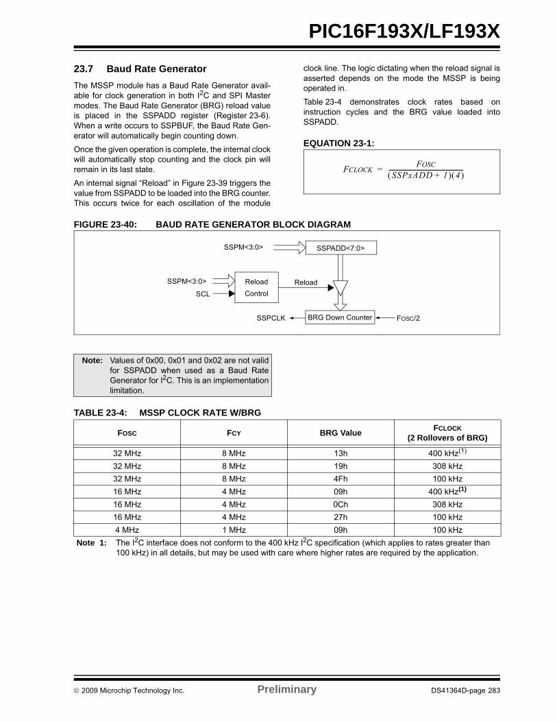
PIC16F193X/LF193X
23.7 Baud Rate Generator
The MSSP module has a Baud Rate Generator avail-able for clock generation in both I2C and SPI Mastermodes. The Baud Rate Generator (BRG) reload valueis placed in the SSPADD register (Register 23-6).When a write occurs to SSPBUF, the Baud Rate Gen-erator will automatically begin counting down.
Once the given operation is complete, the internal clockwill automatically stop counting and the clock pin willremain in its last state.
An internal signal “Reload” in Figure 23-39 triggers thevalue from SSPADD to be loaded into the BRG counter.This occurs twice for each oscillation of the module
clock line. The logic dictating when the reload signal isasserted depends on the mode the MSSP is beingoperated in.
Table 23-4 demonstrates clock rates based oninstruction cycles and the BRG value loaded intoSSPADD.
EQUATION 23-1:
FIGURE 23-40: BAUD RATE GENERATOR BLOCK DIAGRAM
TABLE 23-4: MSSP CLOCK RATE W/BRG
FCLOCKFOSC
SSPxADD 1+ 4 -------------------------------------------------=
Note: Values of 0x00, 0x01 and 0x02 are not validfor SSPADD when used as a Baud RateGenerator for I2C. This is an implementationlimitation.
FOSC FCY BRG ValueFCLOCK
(2 Rollovers of BRG)
32 MHz 8 MHz 13h 400 kHz(1)
32 MHz 8 MHz 19h 308 kHz
32 MHz 8 MHz 4Fh 100 kHz
16 MHz 4 MHz 09h 400 kHz(1)
16 MHz 4 MHz 0Ch 308 kHz
16 MHz 4 MHz 27h 100 kHz
4 MHz 1 MHz 09h 100 kHz
Note 1: The I2C interface does not conform to the 400 kHz I2C specification (which applies to rates greater than 100 kHz) in all details, but may be used with care where higher rates are required by the application.
SSPM<3:0>
BRG Down CounterSSPCLK FOSC/2
SSPADD<7:0>
SSPM<3:0>
SCL
Reload
Control
Reload
2009 Microchip Technology Inc. Preliminary DS41364D-page 283
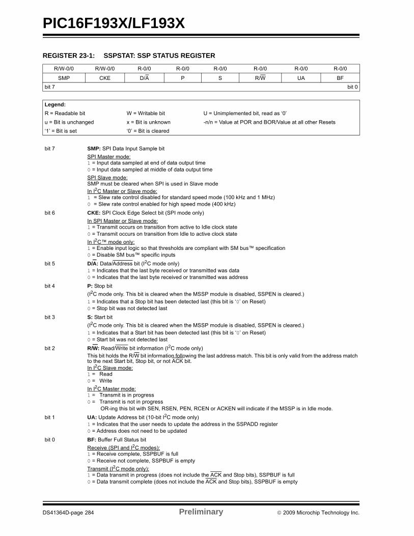
PIC16F193X/LF193X
REGISTER 23-1: SSPSTAT: SSP STATUS REGISTER
R/W-0/0 R/W-0/0 R-0/0 R-0/0 R-0/0 R-0/0 R-0/0 R-0/0
SMP CKE D/A P S R/W UA BF
bit 7 bit 0
Legend:
R = Readable bit W = Writable bit U = Unimplemented bit, read as ‘0’
u = Bit is unchanged x = Bit is unknown -n/n = Value at POR and BOR/Value at all other Resets
‘1’ = Bit is set ‘0’ = Bit is cleared
bit 7 SMP: SPI Data Input Sample bit
SPI Master mode:1 = Input data sampled at end of data output time0 = Input data sampled at middle of data output time
SPI Slave mode:SMP must be cleared when SPI is used in Slave modeIn I2 C Master or Slave mode: 1 = Slew rate control disabled for standard speed mode (100 kHz and 1 MHz)0 = Slew rate control enabled for high speed mode (400 kHz)
bit 6 CKE: SPI Clock Edge Select bit (SPI mode only)
In SPI Master or Slave mode:1 = Transmit occurs on transition from active to Idle clock state0 = Transmit occurs on transition from Idle to active clock state
In I2 C™ mode only: 1 = Enable input logic so that thresholds are compliant with SM bus™ specification0 = Disable SM bus™ specific inputs
bit 5 D/A: Data/Address bit (I2C mode only) 1 = Indicates that the last byte received or transmitted was data0 = Indicates that the last byte received or transmitted was address
bit 4 P: Stop bit
(I2C mode only. This bit is cleared when the MSSP module is disabled, SSPEN is cleared.)1 = Indicates that a Stop bit has been detected last (this bit is ‘0’ on Reset)0 = Stop bit was not detected last
bit 3 S: Start bit
(I2C mode only. This bit is cleared when the MSSP module is disabled, SSPEN is cleared.)1 = Indicates that a Start bit has been detected last (this bit is ‘0’ on Reset)0 = Start bit was not detected last
bit 2 R/W: Read/Write bit information (I2C mode only)This bit holds the R/W bit information following the last address match. This bit is only valid from the address matchto the next Start bit, Stop bit, or not ACK bit.In I2 C Slave mode:1 = Read0 = Write
In I2 C Master mode:1 = Transmit is in progress0 = Transmit is not in progress
OR-ing this bit with SEN, RSEN, PEN, RCEN or ACKEN will indicate if the MSSP is in Idle mode.
bit 1 UA: Update Address bit (10-bit I2C mode only)1 = Indicates that the user needs to update the address in the SSPADD register0 = Address does not need to be updated
bit 0 BF: Buffer Full Status bit
Receive (SPI and I2 C modes):1 = Receive complete, SSPBUF is full0 = Receive not complete, SSPBUF is empty
Transmit (I2 C mode only):1 = Data transmit in progress (does not include the ACK and Stop bits), SSPBUF is full0 = Data transmit complete (does not include the ACK and Stop bits), SSPBUF is empty
DS41364D-page 284 Preliminary 2009 Microchip Technology Inc.
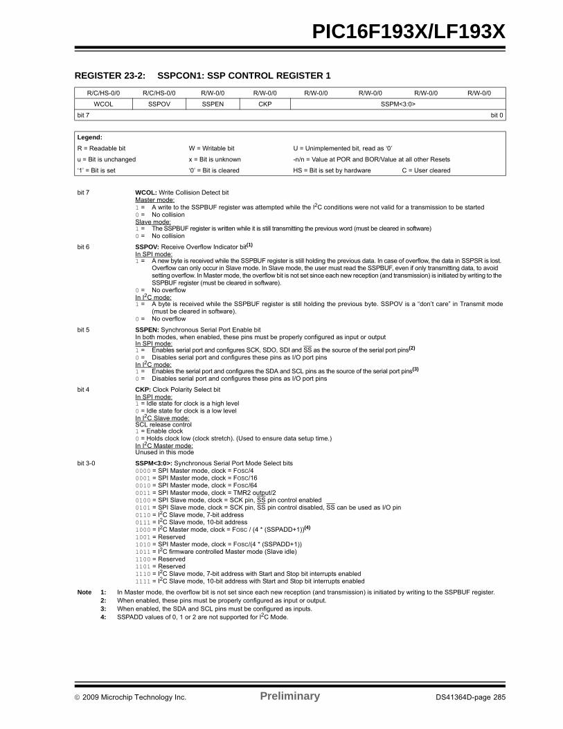
PIC16F193X/LF193X
REGISTER 23-2: SSPCON1: SSP CONTROL REGISTER 1
R/C/HS-0/0 R/C/HS-0/0 R/W-0/0 R/W-0/0 R/W-0/0 R/W-0/0 R/W-0/0 R/W-0/0
WCOL SSPOV SSPEN CKP SSPM<3:0>
bit 7 bit 0
Legend:
R = Readable bit W = Writable bit U = Unimplemented bit, read as ‘0’
u = Bit is unchanged x = Bit is unknown -n/n = Value at POR and BOR/Value at all other Resets
‘1’ = Bit is set ‘0’ = Bit is cleared HS = Bit is set by hardware C = User cleared
bit 7 WCOL: Write Collision Detect bitMaster mode:1 = A write to the SSPBUF register was attempted while the I2C conditions were not valid for a transmission to be started0 = No collisionSlave mode:1 = The SSPBUF register is written while it is still transmitting the previous word (must be cleared in software)0 = No collision
bit 6 SSPOV: Receive Overflow Indicator bit(1)
In SPI mode:1 = A new byte is received while the SSPBUF register is still holding the previous data. In case of overflow, the data in SSPSR is lost.
Overflow can only occur in Slave mode. In Slave mode, the user must read the SSPBUF, even if only transmitting data, to avoid setting overflow. In Master mode, the overflow bit is not set since each new reception (and transmission) is initiated by writing to the SSPBUF register (must be cleared in software).
0 = No overflowIn I2 C mode:1 = A byte is received while the SSPBUF register is still holding the previous byte. SSPOV is a “don’t care” in Transmit mode
(must be cleared in software). 0 = No overflow
bit 5 SSPEN: Synchronous Serial Port Enable bitIn both modes, when enabled, these pins must be properly configured as input or outputIn SPI mode:1 = Enables serial port and configures SCK, SDO, SDI and SS as the source of the serial port pins(2)
0 = Disables serial port and configures these pins as I/O port pinsIn I2 C mode:1 = Enables the serial port and configures the SDA and SCL pins as the source of the serial port pins(3)
0 = Disables serial port and configures these pins as I/O port pins
bit 4 CKP: Clock Polarity Select bit In SPI mode:1 = Idle state for clock is a high level 0 = Idle state for clock is a low levelIn I2 C Slave mode:SCL release control1 = Enable clock 0 = Holds clock low (clock stretch). (Used to ensure data setup time.)In I2 C Master mode:Unused in this mode
bit 3-0 SSPM<3:0>: Synchronous Serial Port Mode Select bits0000 = SPI Master mode, clock = FOSC/40001 = SPI Master mode, clock = FOSC/16 0010 = SPI Master mode, clock = FOSC/64 0011 = SPI Master mode, clock = TMR2 output/2 0100 = SPI Slave mode, clock = SCK pin, SS pin control enabled 0101 = SPI Slave mode, clock = SCK pin, SS pin control disabled, SS can be used as I/O pin0110 = I2C Slave mode, 7-bit address 0111 = I2C Slave mode, 10-bit address 1000 = I2C Master mode, clock = FOSC / (4 * (SSPADD+1))(4)
1001 = Reserved1010 = SPI Master mode, clock = FOSC/(4 * (SSPADD+1))1011 = I2C firmware controlled Master mode (Slave idle) 1100 = Reserved 1101 = Reserved 1110 = I2C Slave mode, 7-bit address with Start and Stop bit interrupts enabled 1111 = I2C Slave mode, 10-bit address with Start and Stop bit interrupts enabled
Note 1: In Master mode, the overflow bit is not set since each new reception (and transmission) is initiated by writing to the SSPBUF register.2: When enabled, these pins must be properly configured as input or output.3: When enabled, the SDA and SCL pins must be configured as inputs.4: SSPADD values of 0, 1 or 2 are not supported for I2C Mode.
2009 Microchip Technology Inc. Preliminary DS41364D-page 285
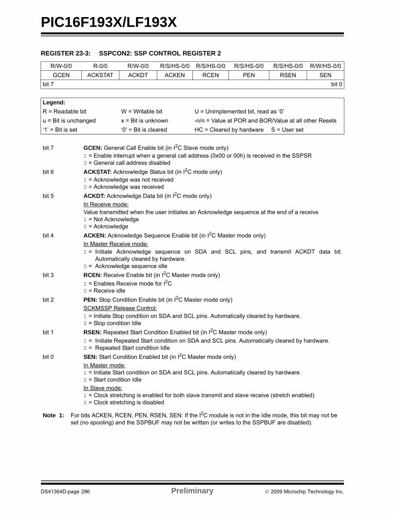
PIC16F193X/LF193X
REGISTER 23-3: SSPCON2: SSP CONTROL REGISTER 2
R/W-0/0 R-0/0 R/W-0/0 R/S/HS-0/0 R/S/HS-0/0 R/S/HS-0/0 R/S/HS-0/0 R/W/HS-0/0
GCEN ACKSTAT ACKDT ACKEN RCEN PEN RSEN SEN
bit 7 bit 0
Legend:
R = Readable bit W = Writable bit U = Unimplemented bit, read as ‘0’
u = Bit is unchanged x = Bit is unknown -n/n = Value at POR and BOR/Value at all other Resets
‘1’ = Bit is set ‘0’ = Bit is cleared HC = Cleared by hardware S = User set
bit 7 GCEN: General Call Enable bit (in I2C Slave mode only)1 = Enable interrupt when a general call address (0x00 or 00h) is received in the SSPSR0 = General call address disabled
bit 6 ACKSTAT: Acknowledge Status bit (in I2C mode only)1 = Acknowledge was not received0 = Acknowledge was received
bit 5 ACKDT: Acknowledge Data bit (in I2C mode only)
In Receive mode:Value transmitted when the user initiates an Acknowledge sequence at the end of a receive1 = Not Acknowledge0 = Acknowledge
bit 4 ACKEN: Acknowledge Sequence Enable bit (in I2C Master mode only)
In Master Receive mode:1 = Initiate Acknowledge sequence on SDA and SCL pins, and transmit ACKDT data bit.
Automatically cleared by hardware.0 = Acknowledge sequence idle
bit 3 RCEN: Receive Enable bit (in I2C Master mode only)
1 = Enables Receive mode for I2C0 = Receive idle
bit 2 PEN: Stop Condition Enable bit (in I2C Master mode only)
SCKMSSP Release Control:1 = Initiate Stop condition on SDA and SCL pins. Automatically cleared by hardware.0 = Stop condition Idle
bit 1 RSEN: Repeated Start Condition Enabled bit (in I2C Master mode only)
1 = Initiate Repeated Start condition on SDA and SCL pins. Automatically cleared by hardware.0 = Repeated Start condition Idle
bit 0 SEN: Start Condition Enabled bit (in I2C Master mode only)
In Master mode:1 = Initiate Start condition on SDA and SCL pins. Automatically cleared by hardware.0 = Start condition Idle
In Slave mode:1 = Clock stretching is enabled for both slave transmit and slave receive (stretch enabled)0 = Clock stretching is disabled
Note 1: For bits ACKEN, RCEN, PEN, RSEN, SEN: If the I2C module is not in the Idle mode, this bit may not be set (no spooling) and the SSPBUF may not be written (or writes to the SSPBUF are disabled).
DS41364D-page 286 Preliminary 2009 Microchip Technology Inc.
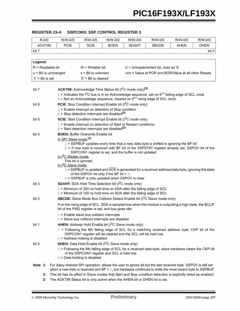
PIC16F193X/LF193X
REGISTER 23-4: SSPCON3: SSP CONTROL REGISTER 3
R-0/0 R/W-0/0 R/W-0/0 R/W-0/0 R/W-0/0 R/W-0/0 R/W-0/0 R/W-0/0
ACKTIM PCIE SCIE BOEN SDAHT SBCDE AHEN DHEN
bit 7 bit 0
Legend:
R = Readable bit W = Writable bit U = Unimplemented bit, read as ‘0’
u = Bit is unchanged x = Bit is unknown -n/n = Value at POR and BOR/Value at all other Resets
‘1’ = Bit is set ‘0’ = Bit is cleared
bit 7 ACKTIM: Acknowledge Time Status bit (I2C mode only)(3)
1 = Indicates the I2C bus is in an Acknowledge sequence, set on 8TH falling edge of SCL clock0 = Not an Acknowledge sequence, cleared on 9TH rising edge of SCL clock
bit 6 PCIE: Stop Condition Interrupt Enable bit (I2C mode only)
1 = Enable interrupt on detection of Stop condition0 = Stop detection interrupts are disabled(2)
bit 5 SCIE: Start Condition Interrupt Enable bit (I2C mode only)
1 = Enable interrupt on detection of Start or Restart conditions0 = Start detection interrupts are disabled(2)
bit 4 BOEN: Buffer Overwrite Enable bit
In SPI Slave mode:(1)
1 = SSPBUF updates every time that a new data byte is shifted in ignoring the BF bit0 = If new byte is received with BF bit of the SSPSTAT register already set, SSPOV bit of the
SSPCON1 register is set, and the buffer is not updatedIn I2C Master mode:
This bit is ignored.In I2C Slave mode:
1 = SSPBUF is updated and ACK is generated for a received address/data byte, ignoring the stateof the SSPOV bit only if the BF bit = 0.
0 = SSPBUF is only updated when SSPOV is clear
bit 3 SDAHT: SDA Hold Time Selection bit (I2C mode only)
1 = Minimum of 300 ns hold time on SDA after the falling edge of SCL0 = Minimum of 100 ns hold time on SDA after the falling edge of SCL
bit 2 SBCDE: Slave Mode Bus Collision Detect Enable bit (I2C Slave mode only)
If on the rising edge of SCL, SDA is sampled low when the module is outputting a high state, the BCLIFbit of the PIR2 register is set, and bus goes idle
1 = Enable slave bus collision interrupts0 = Slave bus collision interrupts are disabled
bit 1 AHEN: Address Hold Enable bit (I2C Slave mode only)
1 = Following the 8th falling edge of SCL for a matching received address byte; CKP bit of theSSPCON1 register will be cleared and the SCL will be held low.
0 = Address holding is disabled
bit 0 DHEN: Data Hold Enable bit (I2C Slave mode only)
1 = Following the 8th falling edge of SCL for a received data byte; slave hardware clears the CKP bitof the SSPCON1 register and SCL is held low.
0 = Data holding is disabled
Note 1: For daisy-chained SPI operation; allows the user to ignore all but the last received byte. SSPOV is still set when a new byte is received and BF = 1, but hardware continues to write the most recent byte to SSPBUF.
2: This bit has no effect in Slave modes that Start and Stop condition detection is explicitly listed as enabled.
3: The ACKTIM Status bit is only active when the AHEN bit or DHEN bit is set.
2009 Microchip Technology Inc. Preliminary DS41364D-page 287

PIC16F193X/LF193X
REGISTER 23-5: SSPMSK: SSP MASK REGISTER
R/W-1/1 R/W-1/1 R/W-1/1 R/W-1/1 R/W-1/1 R/W-1/1 R/W-1/1 R/W-1/1
MSK<7:0>
bit 7 bit 0
Legend:
R = Readable bit W = Writable bit U = Unimplemented bit, read as ‘0’
u = Bit is unchanged x = Bit is unknown -n/n = Value at POR and BOR/Value at all other Resets
‘1’ = Bit is set ‘0’ = Bit is cleared
bit 7-1 MSK<7:1>: Mask bits1 = The received address bit n is compared to SSPADD<n> to detect I2C address match0 = The received address bit n is not used to detect I2C address match
bit 0 MSK<0>: Mask bit for I2C Slave mode, 10-bit AddressI2C Slave mode, 10-bit address (SSPM<3:0> = 0111 or 1111):1 = The received address bit 0 is compared to SSPADD<0> to detect I2C address match0 = The received address bit 0 is not used to detect I2C address matchI2C Slave mode, 7-bit address, the bit is ignored
REGISTER 23-6: SSPADD: MSSP ADDRESS AND BAUD RATE REGISTER (I2C MODE)
R/W-0/0 R/W-0/0 R/W-0/0 R/W-0/0 R/W-0/0 R/W-0/0 R/W-0/0 R/W-0/0
ADD<7:0>
bit 7 bit 0
Legend:
R = Readable bit W = Writable bit U = Unimplemented bit, read as ‘0’
u = Bit is unchanged x = Bit is unknown -n/n = Value at POR and BOR/Value at all other Resets
‘1’ = Bit is set ‘0’ = Bit is cleared
Master mode:
bit 7-0 ADD<7:0>: Baud Rate Clock Divider bitsSCL pin clock period = ((ADD<7:0> + 1) *4)/FOSC
10-Bit Slave mode — Most Significant Address byte:
bit 7-3 Not used: Unused for Most Significant Address byte. Bit state of this register is a “don’t care”. Bit pat-tern sent by master is fixed by I2C specification and must be equal to ‘11110’. However, those bits are compared by hardware and are not affected by the value in this register.
bit 2-1 ADD<2:1>: Two Most Significant bits of 10-bit address
bit 0 Not used: Unused in this mode. Bit state is a “don’t care”.
10-Bit Slave mode — Least Significant Address byte:
bit 7-0 ADD<7:0>: Eight Least Significant bits of 10-bit address
7-Bit Slave mode:
bit 7-1 ADD<7:1>: 7-bit address
bit 0 Not used: Unused in this mode. Bit state is a “don’t care”.
DS41364D-page 288 Preliminary 2009 Microchip Technology Inc.
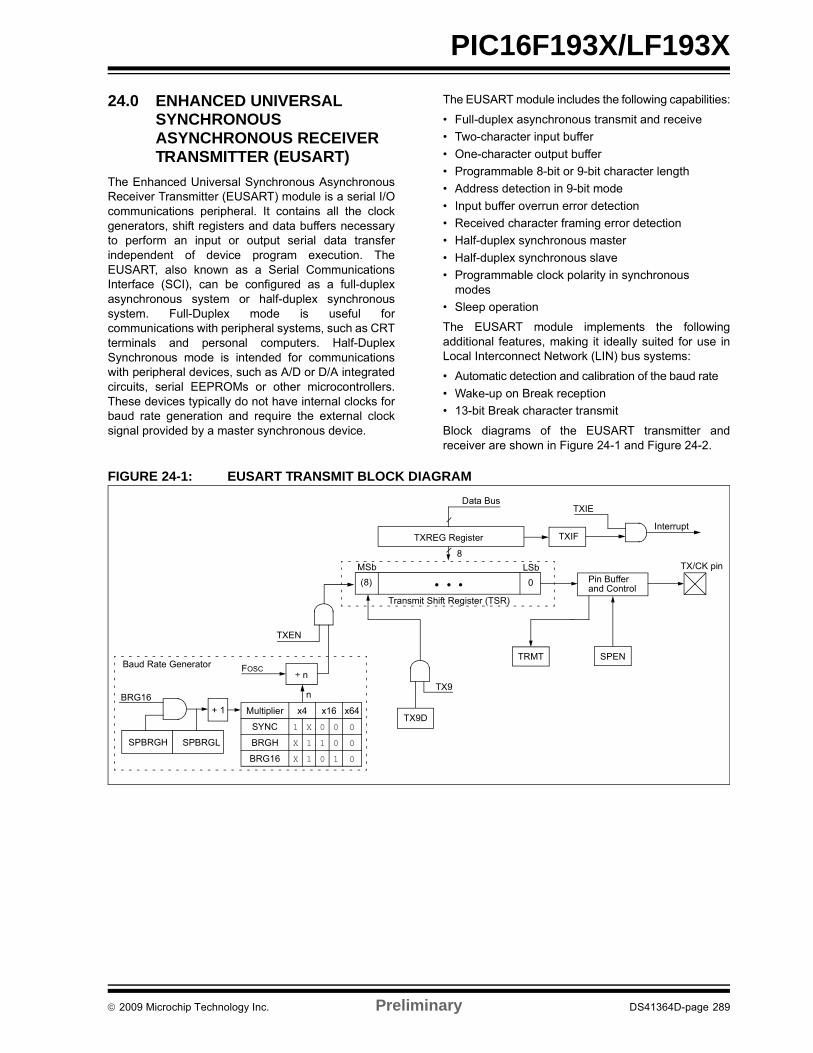
PIC16F193X/LF193X
24.0 ENHANCED UNIVERSAL SYNCHRONOUS ASYNCHRONOUS RECEIVER TRANSMITTER (EUSART)
The Enhanced Universal Synchronous AsynchronousReceiver Transmitter (EUSART) module is a serial I/Ocommunications peripheral. It contains all the clockgenerators, shift registers and data buffers necessaryto perform an input or output serial data transferindependent of device program execution. TheEUSART, also known as a Serial CommunicationsInterface (SCI), can be configured as a full-duplexasynchronous system or half-duplex synchronoussystem. Full-Duplex mode is useful forcommunications with peripheral systems, such as CRTterminals and personal computers. Half-DuplexSynchronous mode is intended for communicationswith peripheral devices, such as A/D or D/A integratedcircuits, serial EEPROMs or other microcontrollers.These devices typically do not have internal clocks forbaud rate generation and require the external clocksignal provided by a master synchronous device.
The EUSART module includes the following capabilities:
• Full-duplex asynchronous transmit and receive
• Two-character input buffer
• One-character output buffer
• Programmable 8-bit or 9-bit character length
• Address detection in 9-bit mode
• Input buffer overrun error detection
• Received character framing error detection
• Half-duplex synchronous master
• Half-duplex synchronous slave
• Programmable clock polarity in synchronous modes
• Sleep operation
The EUSART module implements the followingadditional features, making it ideally suited for use inLocal Interconnect Network (LIN) bus systems:
• Automatic detection and calibration of the baud rate
• Wake-up on Break reception
• 13-bit Break character transmit
Block diagrams of the EUSART transmitter andreceiver are shown in Figure 24-1 and Figure 24-2.
FIGURE 24-1: EUSART TRANSMIT BLOCK DIAGRAM
TXIF
TXIE
Interrupt
TXEN
TX9D
MSb LSb
Data Bus
TXREG Register
Transmit Shift Register (TSR)
(8) 0
TX9
TRMT SPEN
TX/CK pin
Pin Bufferand Control
8
SPBRGLSPBRGH
BRG16
FOSC÷ n
n
+ 1 Multiplier x4 x16 x64
SYNC 1 X 0 0 0
BRGH X 1 1 0 0
BRG16 X 1 0 1 0
Baud Rate Generator
• • •
2009 Microchip Technology Inc. Preliminary DS41364D-page 289

PIC16F193X/LF193X
FIGURE 24-2: EUSART RECEIVE BLOCK DIAGRAM
The operation of the EUSART module is controlledthrough three registers:
• Transmit Status and Control (TXSTA)
• Receive Status and Control (RCSTA)
• Baud Rate Control (BAUDCON)
These registers are detailed in Register 24-1,Register 24-2 and Register 24-3, respectively.
When the receiver or transmitter section is not enabledthen the corresponding RX or TX pin may be used forgeneral purpose input and output.
RX/DT pin
Pin Bufferand Control
SPEN
DataRecovery
CREN OERR
FERR
RSR RegisterMSb LSb
RX9D RCREG RegisterFIFO
InterruptRCIFRCIE
Data Bus8
Stop START(8) 7 1 0
RX9
• • •
SPBRGLSPBRGH
BRG16
RCIDL
FOSC÷ n
n+ 1 Multiplier x4 x16 x64
SYNC 1 X 0 0 0
BRGH X 1 1 0 0
BRG16 X 1 0 1 0
Baud Rate Generator
DS41364D-page 290 Preliminary 2009 Microchip Technology Inc.

PIC16F193X/LF193X
24.1 EUSART Asynchronous Mode
The EUSART transmits and receives data using thestandard non-return-to-zero (NRZ) format. NRZ isimplemented with two levels: a VOH mark state whichrepresents a ‘1’ data bit, and a VOL space state whichrepresents a ‘0’ data bit. NRZ refers to the fact thatconsecutively transmitted data bits of the same valuestay at the output level of that bit without returning to aneutral level between each bit transmission. An NRZtransmission port idles in the mark state. Each charactertransmission consists of one Start bit followed by eightor nine data bits and is always terminated by one ormore Stop bits. The Start bit is always a space and theStop bits are always marks. The most common dataformat is 8 bits. Each transmitted bit persists for a periodof 1/(Baud Rate). An on-chip dedicated 8-bit/16-bit BaudRate Generator is used to derive standard baud ratefrequencies from the system oscillator. See Table 24-5for examples of baud rate configurations.
The EUSART transmits and receives the LSb first. TheEUSART’s transmitter and receiver are functionallyindependent, but share the same data format and baudrate. Parity is not supported by the hardware, but canbe implemented in software and stored as the ninthdata bit.
24.1.1 EUSART ASYNCHRONOUS TRANSMITTER
The EUSART transmitter block diagram is shown inFigure 24-1. The heart of the transmitter is the serialTransmit Shift Register (TSR), which is not directlyaccessible by software. The TSR obtains its data fromthe transmit buffer, which is the TXREG register.
24.1.1.1 Enabling the Transmitter
The EUSART transmitter is enabled for asynchronousoperations by configuring the following three controlbits:
• TXEN = 1
• SYNC = 0
• SPEN = 1
All other EUSART control bits are assumed to be intheir default state.
Setting the TXEN bit of the TXSTA register enables thetransmitter circuitry of the EUSART. Clearing the SYNCbit of the TXSTA register configures the EUSART forasynchronous operation. Setting the SPEN bit of theRCSTA register enables the EUSART and automaticallyconfigures the TX/CK I/O pin as an output.
24.1.1.2 Transmitting Data
A transmission is initiated by writing a character to theTXREG register. If this is the first character, or theprevious character has been completely flushed fromthe TSR, the data in the TXREG is immediatelytransferred to the TSR register. If the TSR still containsall or part of a previous character, the new characterdata is held in the TXREG until the Stop bit of theprevious character has been transmitted. The pendingcharacter in the TXREG is then transferred to the TSRin one TCY immediately following the Stop bittransmission. The transmission of the Start bit, data bitsand Stop bit sequence commences immediatelyfollowing the transfer of the data to the TSR from theTXREG.
24.1.1.3 Transmit Interrupt Flag
The TXIF interrupt flag bit of the PIR1 register is setwhenever the EUSART transmitter is enabled and nocharacter is being held for transmission in the TXREG.In other words, the TXIF bit is only clear when the TSRis busy with a character and a new character has beenqueued for transmission in the TXREG. The TXIF flag bitis not cleared immediately upon writing TXREG. TXIFbecomes valid in the second instruction cycle followingthe write execution. Polling TXIF immediately followingthe TXREG write will return invalid results. The TXIF bitis read-only, it cannot be set or cleared by software.
The TXIF interrupt can be enabled by setting the TXIEinterrupt enable bit of the PIE1 register. However, theTXIF flag bit will be set whenever the TXREG is empty,regardless of the state of TXIE enable bit.
To use interrupts when transmitting data, set the TXIEbit only when there is more data to send. Clear theTXIE interrupt enable bit upon writing the last characterof the transmission to the TXREG.
Note 1: The TXIF Transmitter Interrupt flag is setwhen the TXEN enable bit is set.
2009 Microchip Technology Inc. Preliminary DS41364D-page 291

PIC16F193X/LF193X
24.1.1.4 TSR Status
The TRMT bit of the TXSTA register indicates thestatus of the TSR register. This is a read-only bit. TheTRMT bit is set when the TSR register is empty and iscleared when a character is transferred to the TSRregister from the TXREG. The TRMT bit remains clearuntil all bits have been shifted out of the TSR register.No interrupt logic is tied to this bit, so the user has topoll this bit to determine the TSR status.
24.1.1.5 Transmitting 9-Bit Characters
The EUSART supports 9-bit character transmissions.When the TX9 bit of the TXSTA register is set, theEUSART will shift 9 bits out for each character transmit-ted. The TX9D bit of the TXSTA register is the ninth,and Most Significant, data bit. When transmitting 9-bitdata, the TX9D data bit must be written before writingthe 8 Least Significant bits into the TXREG. All nine bitsof data will be transferred to the TSR shift registerimmediately after the TXREG is written.
A special 9-bit Address mode is available for use withmultiple receivers. See Section 24.1.2.7 “AddressDetection” for more information on the address mode.
24.1.1.6 Asynchronous Transmission Set-up:
1. Initialize the SPBRGH, SPBRGL register pair andthe BRGH and BRG16 bits to achieve the desiredbaud rate (see Section 24.3 “EUSART BaudRate Generator (BRG)”).
2. Enable the asynchronous serial port by clearingthe SYNC bit and setting the SPEN bit.
3. If 9-bit transmission is desired, set the TX9 con-trol bit. A set ninth data bit will indicate that the 8Least Significant data bits are an address whenthe receiver is set for address detection.
4. Enable the transmission by setting the TXENcontrol bit. This will cause the TXIF interrupt bitto be set.
5. If interrupts are desired, set the TXIE interruptenable bit of the PIE1 register. An interrupt willoccur immediately provided that the GIE andPEIE bits of the INTCON register are also set.
6. If 9-bit transmission is selected, the ninth bitshould be loaded into the TX9D data bit.
7. Load 8-bit data into the TXREG register. Thiswill start the transmission.
FIGURE 24-3: ASYNCHRONOUS TRANSMISSION
FIGURE 24-4: ASYNCHRONOUS TRANSMISSION (BACK-TO-BACK)
Note: The TSR register is not mapped in datamemory, so it is not available to the user.
Word 1Stop bit
Word 1Transmit Shift Reg.
Start bit bit 0 bit 1 bit 7/8
Write to TXREGWord 1
BRG Output(Shift Clock)
TX/CK
TXIF bit(Transmit Buffer
Reg. Empty Flag)
TRMT bit(Transmit Shift
Reg. Empty Flag)
1 TCY
pin
Transmit Shift Reg.
Write to TXREG
BRG Output(Shift Clock)
TX/CK
TRMT bit(Transmit Shift
Reg. Empty Flag)
Word 1 Word 2
Word 1 Word 2
Start bit Stop bit Start bit
Transmit Shift Reg.
Word 1 Word 2bit 0 bit 1 bit 7/8 bit 0
Note: This timing diagram shows two consecutive transmissions.
1 TCY
1 TCY
pin
TXIF bit(Transmit Buffer
Reg. Empty Flag)
DS41364D-page 292 Preliminary 2009 Microchip Technology Inc.

PIC16F193X/LF193X
TABLE 24-1: SUMMARY OF REGISTERS ASSOCIATED WITH ASYNCHRONOUS TRANSMISSION
Name Bit 7 Bit 6 Bit 5 Bit 4 Bit 3 Bit 2 Bit 1 Bit 0Register on Page
BAUDCON ABDOVF RCIDL — SCKP BRG16 — WUE ABDEN 300
INTCON GIE PEIE TMR0IE INTE IOCIE TMR0IF INTF IOCIF 99
PIE1 TMR1GIE ADIE RCIE TXIE SSPIE CCP1IE TMR2IE TMR1IE 100
PIR1 TMR1GIF ADIF RCIF TXIF SSPIF CCP1IF TMR2IF TMR1IF 103
RCSTA SPEN RX9 SREN CREN ADDEN FERR OERR RX9D 299
SPBRGL BRG<7:0> 301*
SPBRGH BRG<15:8> 301*
TRISC TRISC7 TRISC6 TRISC5 TRISC4 TRISC3 TRISC2 TRISC1 TRISC0 140
TXREG EUSART Transmit Data Register 291*
TXSTA CSRC TX9 TXEN SYNC SENDB BRGH TRMT TX9D 298
Legend: x = unknown, - = unimplemented read as ‘0’. Shaded cells are not used for Asynchronous Transmission.
* Page provides register information.
2009 Microchip Technology Inc. Preliminary DS41364D-page 293

PIC16F193X/LF193X
24.1.2 EUSART ASYNCHRONOUS RECEIVER
The Asynchronous mode is typically used in RS-232systems. The receiver block diagram is shown inFigure 24-2. The data is received on the RX/DT pin anddrives the data recovery block. The data recovery blockis actually a high-speed shifter operating at 16 timesthe baud rate, whereas the serial Receive ShiftRegister (RSR) operates at the bit rate. When all 8 or 9bits of the character have been shifted in, they areimmediately transferred to a two characterFirst-In-First-Out (FIFO) memory. The FIFO bufferingallows reception of two complete characters and thestart of a third character before software must startservicing the EUSART receiver. The FIFO and RSRregisters are not directly accessible by software.Access to the received data is via the RCREG register.
24.1.2.1 Enabling the Receiver
The EUSART receiver is enabled for asynchronousoperation by configuring the following three control bits:
• CREN = 1
• SYNC = 0
• SPEN = 1
All other EUSART control bits are assumed to be intheir default state.
Setting the CREN bit of the RCSTA register enables thereceiver circuitry of the EUSART. Clearing the SYNC bitof the TXSTA register configures the EUSART forasynchronous operation. Setting the SPEN bit of theRCSTA register enables the EUSART and automaticallyconfigures the RX/DT I/O pin as an input.
24.1.2.2 Receiving Data
The receiver data recovery circuit initiates characterreception on the falling edge of the first bit. The first bit,also known as the Start bit, is always a zero. The datarecovery circuit counts one-half bit time to the center ofthe Start bit and verifies that the bit is still a zero. If it isnot a zero then the data recovery circuit abortscharacter reception, without generating an error, andresumes looking for the falling edge of the Start bit. Ifthe Start bit zero verification succeeds then the datarecovery circuit counts a full bit time to the center of thenext bit. The bit is then sampled by a majority detectcircuit and the resulting ‘0’ or ‘1’ is shifted into the RSR.This repeats until all data bits have been sampled andshifted into the RSR. One final bit time is measured andthe level sampled. This is the Stop bit, which is alwaysa ‘1’. If the data recovery circuit samples a ‘0’ in theStop bit position then a framing error is set for thischaracter, otherwise the framing error is cleared for thischaracter. See Section 24.1.2.4 “Receive FramingError” for more information on framing errors.
Immediately after all data bits and the Stop bit havebeen received, the character in the RSR is transferredto the EUSART receive FIFO and the RCIF interruptflag bit of the PIR1 register is set. The top character inthe FIFO is transferred out of the FIFO by reading theRCREG register.
24.1.2.3 Receive Interrupts
The RCIF interrupt flag bit of the PIR1 register is setwhenever the EUSART receiver is enabled and there isan unread character in the receive FIFO. The RCIFinterrupt flag bit is read-only, it cannot be set or clearedby software.
RCIF interrupts are enabled by setting all of thefollowing bits:
• RCIE interrupt enable bit of the PIE1 register
• PEIE peripheral interrupt enable bit of the INTCON register
• GIE global interrupt enable bit of the INTCON register
The RCIF interrupt flag bit will be set when there is anunread character in the FIFO, regardless of the state ofinterrupt enable bits.
Note 1: When the SPEN bit is set the TX/CK I/Opin is automatically configured as anoutput, regardless of the state of thecorresponding TRIS bit and whether or notthe EUSART transmitter is enabled. ThePORT latch is disconnected from theoutput driver so it is not possible to use theTX/CK pin as a general purpose output.
2: If the RX/DT function is on an analog pin,the corresponding ANSEL bit must becleared for the receiver to function.
Note: If the receive FIFO is overrun, no additionalcharacters will be received until the overruncondition is cleared. See Section 24.1.2.5“Receive Overrun Error” for moreinformation on overrun errors.
DS41364D-page 294 Preliminary 2009 Microchip Technology Inc.
PIC16F193X/LF193X
24.1.2.4 Receive Framing Error
Each character in the receive FIFO buffer has acorresponding framing error Status bit. A framing errorindicates that a Stop bit was not seen at the expectedtime. The framing error status is accessed via theFERR bit of the RCSTA register. The FERR bitrepresents the status of the top unread character in thereceive FIFO. Therefore, the FERR bit must be readbefore reading the RCREG.
The FERR bit is read-only and only applies to the topunread character in the receive FIFO. A framing error(FERR = 1) does not preclude reception of additionalcharacters. It is not necessary to clear the FERR bit.Reading the next character from the FIFO buffer willadvance the FIFO to the next character and the nextcorresponding framing error.
The FERR bit can be forced clear by clearing the SPENbit of the RCSTA register which resets the EUSART.Clearing the CREN bit of the RCSTA register does notaffect the FERR bit. A framing error by itself does notgenerate an interrupt.
24.1.2.5 Receive Overrun Error
The receive FIFO buffer can hold two characters. Anoverrun error will be generated if a third character, in itsentirety, is received before the FIFO is accessed. Whenthis happens the OERR bit of the RCSTA register is set.The characters already in the FIFO buffer can be readbut no additional characters will be received until theerror is cleared. The error must be cleared by eitherclearing the CREN bit of the RCSTA register or byresetting the EUSART by clearing the SPEN bit of theRCSTA register.
24.1.2.6 Receiving 9-bit Characters
The EUSART supports 9-bit character reception. Whenthe RX9 bit of the RCSTA register is set the EUSARTwill shift 9 bits into the RSR for each characterreceived. The RX9D bit of the RCSTA register is theninth and Most Significant data bit of the top unreadcharacter in the receive FIFO. When reading 9-bit datafrom the receive FIFO buffer, the RX9D data bit mustbe read before reading the 8 Least Significant bits fromthe RCREG.
24.1.2.7 Address Detection
A special Address Detection mode is available for usewhen multiple receivers share the same transmissionline, such as in RS-485 systems. Address detection isenabled by setting the ADDEN bit of the RCSTAregister.
Address detection requires 9-bit character reception.When address detection is enabled, only characterswith the ninth data bit set will be transferred to thereceive FIFO buffer, thereby setting the RCIF interruptbit. All other characters will be ignored.
Upon receiving an address character, user softwaredetermines if the address matches its own. Uponaddress match, user software must disable addressdetection by clearing the ADDEN bit before the nextStop bit occurs. When user software detects the end ofthe message, determined by the message protocolused, software places the receiver back into theAddress Detection mode by setting the ADDEN bit.
Note: If all receive characters in the receiveFIFO have framing errors, repeated readsof the RCREG will not clear the FERR bit.
2009 Microchip Technology Inc. Preliminary DS41364D-page 295
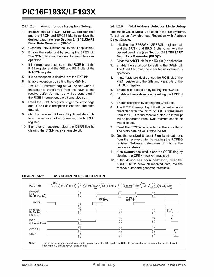
PIC16F193X/LF193X
24.1.2.8 Asynchronous Reception Set-up:
1. Initialize the SPBRGH, SPBRGL register pairand the BRGH and BRG16 bits to achieve thedesired baud rate (see Section 24.3 “EUSARTBaud Rate Generator (BRG)”).
2. Clear the ANSEL bit for the RX pin (if applicable).
3. Enable the serial port by setting the SPEN bit.The SYNC bit must be clear for asynchronousoperation.
4. If interrupts are desired, set the RCIE bit of thePIE1 register and the GIE and PEIE bits of theINTCON register.
5. If 9-bit reception is desired, set the RX9 bit.
6. Enable reception by setting the CREN bit.
7. The RCIF interrupt flag bit will be set when acharacter is transferred from the RSR to thereceive buffer. An interrupt will be generated ifthe RCIE interrupt enable bit was also set.
8. Read the RCSTA register to get the error flagsand, if 9-bit data reception is enabled, the ninthdata bit.
9. Get the received 8 Least Significant data bitsfrom the receive buffer by reading the RCREGregister.
10. If an overrun occurred, clear the OERR flag byclearing the CREN receiver enable bit.
24.1.2.9 9-bit Address Detection Mode Set-up
This mode would typically be used in RS-485 systems.To set up an Asynchronous Reception with AddressDetect Enable:
1. Initialize the SPBRGH, SPBRGL register pairand the BRGH and BRG16 bits to achieve thedesired baud rate (see Section 24.3 “EUSARTBaud Rate Generator (BRG)”).
2. Clear the ANSEL bit for the RX pin (if applicable).
3. Enable the serial port by setting the SPEN bit.The SYNC bit must be clear for asynchronousoperation.
4. If interrupts are desired, set the RCIE bit of thePIE1 register and the GIE and PEIE bits of theINTCON register.
5. Enable 9-bit reception by setting the RX9 bit.
6. Enable address detection by setting the ADDENbit.
7. Enable reception by setting the CREN bit.
8. The RCIF interrupt flag bit will be set when acharacter with the ninth bit set is transferredfrom the RSR to the receive buffer. An interruptwill be generated if the RCIE interrupt enable bitwas also set.
9. Read the RCSTA register to get the error flags.The ninth data bit will always be set.
10. Get the received 8 Least Significant data bitsfrom the receive buffer by reading the RCREGregister. Software determines if this is thedevice’s address.
11. If an overrun occurred, clear the OERR flag byclearing the CREN receiver enable bit.
12. If the device has been addressed, clear theADDEN bit to allow all received data into thereceive buffer and generate interrupts.
FIGURE 24-5: ASYNCHRONOUS RECEPTION
Startbit bit 7/8bit 1bit 0 bit 7/8 bit 0Stop
bit
Startbit
Startbitbit 7/8 Stop
bitRX/DT pin
RegRcv Buffer Reg.
Rcv Shift
Read RcvBuffer Reg.RCREG
RCIF(Interrupt Flag)
OERR bit
CREN
Word 1RCREG
Word 2RCREG
Stopbit
Note: This timing diagram shows three words appearing on the RX input. The RCREG (receive buffer) is read after the third word,causing the OERR (overrun) bit to be set.
RCIDL
DS41364D-page 296 Preliminary 2009 Microchip Technology Inc.
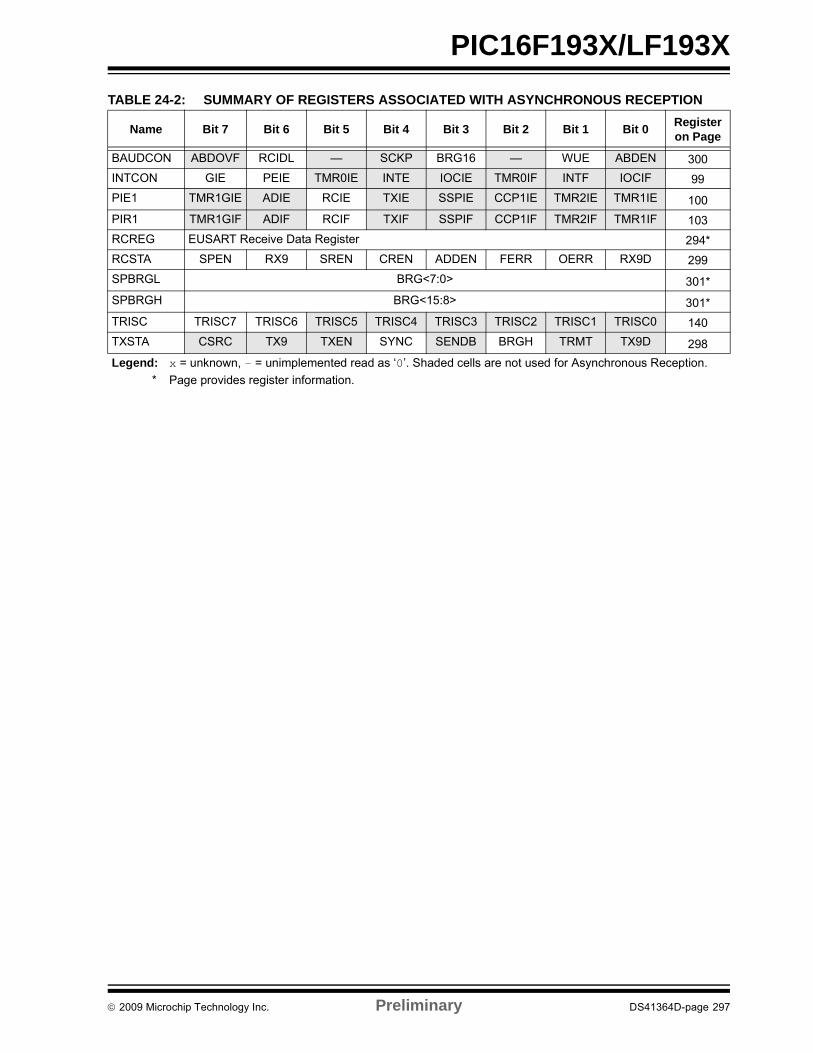
PIC16F193X/LF193X
TABLE 24-2: SUMMARY OF REGISTERS ASSOCIATED WITH ASYNCHRONOUS RECEPTION
Name Bit 7 Bit 6 Bit 5 Bit 4 Bit 3 Bit 2 Bit 1 Bit 0Register on Page
BAUDCON ABDOVF RCIDL — SCKP BRG16 — WUE ABDEN 300
INTCON GIE PEIE TMR0IE INTE IOCIE TMR0IF INTF IOCIF 99
PIE1 TMR1GIE ADIE RCIE TXIE SSPIE CCP1IE TMR2IE TMR1IE 100
PIR1 TMR1GIF ADIF RCIF TXIF SSPIF CCP1IF TMR2IF TMR1IF 103
RCREG EUSART Receive Data Register 294*
RCSTA SPEN RX9 SREN CREN ADDEN FERR OERR RX9D 299
SPBRGL BRG<7:0> 301*
SPBRGH BRG<15:8> 301*
TRISC TRISC7 TRISC6 TRISC5 TRISC4 TRISC3 TRISC2 TRISC1 TRISC0 140
TXSTA CSRC TX9 TXEN SYNC SENDB BRGH TRMT TX9D 298
Legend: x = unknown, - = unimplemented read as ‘0’. Shaded cells are not used for Asynchronous Reception.
* Page provides register information.
2009 Microchip Technology Inc. Preliminary DS41364D-page 297

PIC16F193X/LF193X
24.2 Clock Accuracy with Asynchronous Operation
The factory calibrates the internal oscillator block out-put (INTOSC). However, the INTOSC frequency maydrift as VDD or temperature changes, and this directlyaffects the asynchronous baud rate. Two methods maybe used to adjust the baud rate clock, but both requirea reference clock source of some kind.
The first (preferred) method uses the OSCTUNEregister to adjust the INTOSC output. Adjusting thevalue in the OSCTUNE register allows for fine resolutionchanges to the system clock source. See Section 5.2.2“Internal Clock Sources” for more information.
The other method adjusts the value in the Baud RateGenerator. This can be done automatically with theAuto-Baud Detect feature (see Section 24.3.1“Auto-Baud Detect”). There may not be fine enoughresolution when adjusting the Baud Rate Generator tocompensate for a gradual change in the peripheralclock frequency.
REGISTER 24-1: TXSTA: TRANSMIT STATUS AND CONTROL REGISTER
R/W-/0 R/W-0/0 R/W-0/0 R/W-0/0 R/W-0/0 R/W-0/0 R-1/1 R/W-0/0
CSRC TX9 TXEN(1) SYNC SENDB BRGH TRMT TX9D
bit 7 bit 0
Legend:
R = Readable bit W = Writable bit U = Unimplemented bit, read as ‘0’
u = Bit is unchanged x = Bit is unknown -n/n = Value at POR and BOR/Value at all other Resets
‘1’ = Bit is set ‘0’ = Bit is cleared
bit 7 CSRC: Clock Source Select bitAsynchronous mode: Don’t careSynchronous mode: 1 = Master mode (clock generated internally from BRG)0 = Slave mode (clock from external source)
bit 6 TX9: 9-bit Transmit Enable bit1 = Selects 9-bit transmission0 = Selects 8-bit transmission
bit 5 TXEN: Transmit Enable bit(1)
1 = Transmit enabled0 = Transmit disabled
bit 4 SYNC: EUSART Mode Select bit 1 = Synchronous mode 0 = Asynchronous mode
bit 3 SENDB: Send Break Character bitAsynchronous mode:1 = Send Sync Break on next transmission (cleared by hardware upon completion)0 = Sync Break transmission completedSynchronous mode:Don’t care
bit 2 BRGH: High Baud Rate Select bitAsynchronous mode: 1 = High speed 0 = Low speedSynchronous mode: Unused in this mode
bit 1 TRMT: Transmit Shift Register Status bit1 = TSR empty 0 = TSR full
bit 0 TX9D: Ninth bit of Transmit DataCan be address/data bit or a parity bit.
Note 1: SREN/CREN overrides TXEN in Sync mode.
DS41364D-page 298 Preliminary 2009 Microchip Technology Inc.

PIC16F193X/LF193X
REGISTER 24-2: RCSTA: RECEIVE STATUS AND CONTROL REGISTER(1)
R/W-0/0 R/W-0/0 R/W-0/0 R/W-0/0 R/W-0/0 R-0/0 R-0/0 R-x/x
SPEN RX9 SREN CREN ADDEN FERR OERR RX9D
bit 7 bit 0
Legend:
R = Readable bit W = Writable bit U = Unimplemented bit, read as ‘0’
u = Bit is unchanged x = Bit is unknown -n/n = Value at POR and BOR/Value at all other Resets
‘1’ = Bit is set ‘0’ = Bit is cleared
bit 7 SPEN: Serial Port Enable bit
1 = Serial port enabled (configures RX/DT and TX/CK pins as serial port pins)0 = Serial port disabled (held in Reset)
bit 6 RX9: 9-bit Receive Enable bit
1 = Selects 9-bit reception0 = Selects 8-bit reception
bit 5 SREN: Single Receive Enable bit
Asynchronous mode:
Don’t careSynchronous mode – Master:
1 = Enables single receive0 = Disables single receiveThis bit is cleared after reception is complete.Synchronous mode – Slave
Don’t care
bit 4 CREN: Continuous Receive Enable bit
Asynchronous mode:
1 = Enables receiver0 = Disables receiverSynchronous mode:
1 = Enables continuous receive until enable bit CREN is cleared (CREN overrides SREN)0 = Disables continuous receive
bit 3 ADDEN: Address Detect Enable bit
Asynchronous mode 9-bit (RX9 = 1):
1 = Enables address detection, enable interrupt and load the receive buffer when RSR<8> is set0 = Disables address detection, all bytes are received and ninth bit can be used as parity bitAsynchronous mode 8-bit (RX9 = 0):
Don’t care
bit 2 FERR: Framing Error bit
1 = Framing error (can be updated by reading RCREG register and receive next valid byte)0 = No framing error
bit 1 OERR: Overrun Error bit
1 = Overrun error (can be cleared by clearing bit CREN) 0 = No overrun error
bit 0 RX9D: Ninth bit of Received Data
This can be address/data bit or a parity bit and must be calculated by user firmware.
2009 Microchip Technology Inc. Preliminary DS41364D-page 299
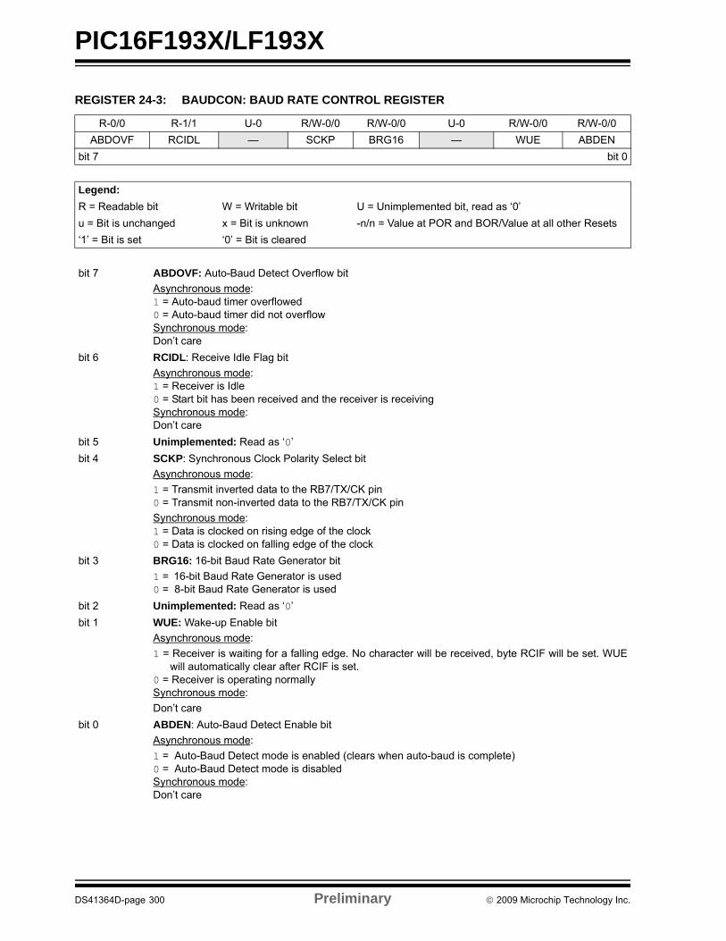
PIC16F193X/LF193X
REGISTER 24-3: BAUDCON: BAUD RATE CONTROL REGISTER
R-0/0 R-1/1 U-0 R/W-0/0 R/W-0/0 U-0 R/W-0/0 R/W-0/0
ABDOVF RCIDL — SCKP BRG16 — WUE ABDEN
bit 7 bit 0
Legend:
R = Readable bit W = Writable bit U = Unimplemented bit, read as ‘0’
u = Bit is unchanged x = Bit is unknown -n/n = Value at POR and BOR/Value at all other Resets
‘1’ = Bit is set ‘0’ = Bit is cleared
bit 7 ABDOVF: Auto-Baud Detect Overflow bit
Asynchronous mode:1 = Auto-baud timer overflowed0 = Auto-baud timer did not overflowSynchronous mode:Don’t care
bit 6 RCIDL: Receive Idle Flag bit
Asynchronous mode:1 = Receiver is Idle0 = Start bit has been received and the receiver is receivingSynchronous mode:Don’t care
bit 5 Unimplemented: Read as ‘0’
bit 4 SCKP: Synchronous Clock Polarity Select bit
Asynchronous mode:
1 = Transmit inverted data to the RB7/TX/CK pin0 = Transmit non-inverted data to the RB7/TX/CK pin
Synchronous mode:1 = Data is clocked on rising edge of the clock0 = Data is clocked on falling edge of the clock
bit 3 BRG16: 16-bit Baud Rate Generator bit
1 = 16-bit Baud Rate Generator is used0 = 8-bit Baud Rate Generator is used
bit 2 Unimplemented: Read as ‘0’
bit 1 WUE: Wake-up Enable bit
Asynchronous mode:
1 = Receiver is waiting for a falling edge. No character will be received, byte RCIF will be set. WUEwill automatically clear after RCIF is set.
0 = Receiver is operating normallySynchronous mode:
Don’t care
bit 0 ABDEN: Auto-Baud Detect Enable bit
Asynchronous mode:
1 = Auto-Baud Detect mode is enabled (clears when auto-baud is complete)0 = Auto-Baud Detect mode is disabledSynchronous mode:Don’t care
DS41364D-page 300 Preliminary 2009 Microchip Technology Inc.

PIC16F193X/LF193X
24.3 EUSART Baud Rate Generator (BRG)
The Baud Rate Generator (BRG) is an 8-bit or 16-bittimer that is dedicated to the support of both theasynchronous and synchronous EUSART operation.By default, the BRG operates in 8-bit mode. Setting theBRG16 bit of the BAUDCON register selects 16-bitmode.
The SPBRGH, SPBRGL register pair determines theperiod of the free running baud rate timer. InAsynchronous mode the multiplier of the baud rateperiod is determined by both the BRGH bit of the TXSTAregister and the BRG16 bit of the BAUDCON register. InSynchronous mode, the BRGH bit is ignored.
Table 24-3 contains the formulas for determining thebaud rate. Example 24-1 provides a sample calculationfor determining the baud rate and baud rate error.
Typical baud rates and error values for variousasynchronous modes have been computed for yourconvenience and are shown in Table 24-3. It may beadvantageous to use the high baud rate (BRGH = 1),or the 16-bit BRG (BRG16 = 1) to reduce the baud rateerror. The 16-bit BRG mode is used to achieve slowbaud rates for fast oscillator frequencies.
Writing a new value to the SPBRGH, SPBRGL registerpair causes the BRG timer to be reset (or cleared). Thisensures that the BRG does not wait for a timer overflowbefore outputting the new baud rate.
If the system clock is changed during an active receiveoperation, a receive error or data loss may result. Toavoid this problem, check the status of the RCIDL bit tomake sure that the receive operation is Idle beforechanging the system clock.
EXAMPLE 24-1: CALCULATING BAUD RATE ERROR
For a device with FOSC of 16 MHz, desired baud rateof 9600, Asynchronous mode, 8-bit BRG:
Solving for SPBRGH:SPBRGL:
X
FOSC
Desired Baud Rate---------------------------------------------
64--------------------------------------------- 1–=
Desired Baud Rate FOSC
64 [SPBRGH:SPBRG] 1+ ---------------------------------------------------------------------=
160000009600
------------------------
64------------------------ 1–=
25.042 25= =
Calculated Baud Rate 16000000
64 25 1+ ---------------------------=
9615=
ErrorCalc. Baud Rate Desired Baud Rate –
Desired Baud Rate --------------------------------------------------------------------------------------------=
9615 9600–
9600---------------------------------- 0.16%= =
2009 Microchip Technology Inc. Preliminary DS41364D-page 301

PIC16F193X/LF193X
TABLE 24-3: BAUD RATE FORMULAS
TABLE 24-4: SUMMARY OF REGISTERS ASSOCIATED WITH THE BAUD RATE GENERATOR
Configuration BitsBRG/EUSART Mode Baud Rate Formula
SYNC BRG16 BRGH
0 0 0 8-bit/Asynchronous FOSC/[64 (n+1)]
0 0 1 8-bit/AsynchronousFOSC/[16 (n+1)]
0 1 0 16-bit/Asynchronous
0 1 1 16-bit/Asynchronous
FOSC/[4 (n+1)]1 0 x 8-bit/Synchronous
1 1 x 16-bit/Synchronous
Legend: x = Don’t care, n = value of SPBRGH, SPBRGL register pair
Name Bit 7 Bit 6 Bit 5 Bit 4 Bit 3 Bit 2 Bit 1 Bit 0Register on Page
BAUDCON ABDOVF RCIDL — SCKP BRG16 — WUE ABDEN 300
RCSTA SPEN RX9 SREN CREN ADDEN FERR OERR RX9D 299
SPBRGL BRG<7:0> 301*
SPBRGH BRG<15:8> 301*
TXSTA CSRC TX9 TXEN SYNC SENDB BRGH TRMT TX9D 298
Legend: x = unknown, - = unimplemented read as ‘0’. Shaded cells are not used for the Baud Rate Generator.
* Page provides register information.
DS41364D-page 302 Preliminary 2009 Microchip Technology Inc.
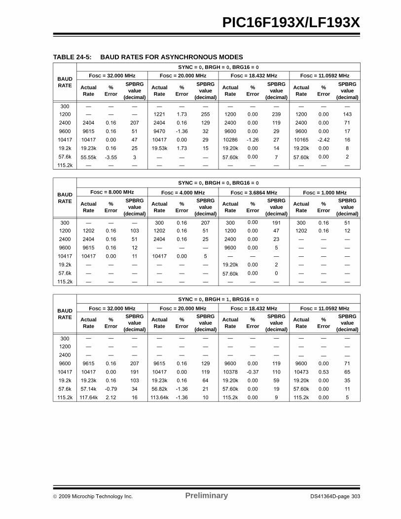
PIC16F193X/LF193X
TABLE 24-5: BAUD RATES FOR ASYNCHRONOUS MODES
BAUDRATE
SYNC = 0, BRGH = 0, BRG16 = 0
FOSC = 32.000 MHz FOSC = 20.000 MHz FOSC = 18.432 MHz FOSC = 11.0592 MHz
ActualRate
%Error
SPBRGvalue
(decimal)
ActualRate
%Error
SPBRGvalue
(decimal)
ActualRate
%Error
SPBRGvalue
(decimal)
ActualRate
%Error
SPBRGvalue
(decimal)
300 — — — — — — — — — — — —
1200 — — — 1221 1.73 255 1200 0.00 239 1200 0.00 143
2400 2404 0.16 207 2404 0.16 129 2400 0.00 119 2400 0.00 71
9600 9615 0.16 51 9470 -1.36 32 9600 0.00 29 9600 0.00 17
10417 10417 0.00 47 10417 0.00 29 10286 -1.26 27 10165 -2.42 16
19.2k 19.23k 0.16 25 19.53k 1.73 15 19.20k 0.00 14 19.20k 0.00 8
57.6k 55.55k -3.55 3 — — — 57.60k 0.00 7 57.60k 0.00 2
115.2k — — — — — — — — — — — —
BAUDRATE
SYNC = 0, BRGH = 0, BRG16 = 0
FOSC = 8.000 MHz FOSC = 4.000 MHz FOSC = 3.6864 MHz FOSC = 1.000 MHz
ActualRate
%Error
SPBRGvalue
(decimal)
ActualRate
%Error
SPBRGvalue
(decimal)
ActualRate
%Error
SPBRGvalue
(decimal)
ActualRate
%Error
SPBRGvalue
(decimal)
300 — — — 300 0.16 207 300 0.00 191 300 0.16 51
1200 1202 0.16 103 1202 0.16 51 1200 0.00 47 1202 0.16 12
2400 2404 0.16 51 2404 0.16 25 2400 0.00 23 — — —
9600 9615 0.16 12 — — — 9600 0.00 5 — — —
10417 10417 0.00 11 10417 0.00 5 — — — — — —
19.2k — — — — — — 19.20k 0.00 2 — — —
57.6k — — — — — — 57.60k 0.00 0 — — —
115.2k — — — — — — — — — — — —
BAUDRATE
SYNC = 0, BRGH = 1, BRG16 = 0
FOSC = 32.000 MHz FOSC = 20.000 MHz FOSC = 18.432 MHz FOSC = 11.0592 MHz
ActualRate
%Error
SPBRGvalue
(decimal)
ActualRate
%Error
SPBRGvalue
(decimal)
ActualRate
%Error
SPBRGvalue
(decimal)
ActualRate
%Error
SPBRGvalue
(decimal)
300 — — — — — — — — — — — —
1200 — — — — — — — — — — — —
2400 — — — — — — — — — — — —
9600 9615 0.16 207 9615 0.16 129 9600 0.00 119 9600 0.00 71
10417 10417 0.00 191 10417 0.00 119 10378 -0.37 110 10473 0.53 65
19.2k 19.23k 0.16 103 19.23k 0.16 64 19.20k 0.00 59 19.20k 0.00 35
57.6k 57.14k -0.79 34 56.82k -1.36 21 57.60k 0.00 19 57.60k 0.00 11
115.2k 117.64k 2.12 16 113.64k -1.36 10 115.2k 0.00 9 115.2k 0.00 5
2009 Microchip Technology Inc. Preliminary DS41364D-page 303

PIC16F193X/LF193X
BAUDRATE
SYNC = 0, BRGH = 1, BRG16 = 0
FOSC = 8.000 MHz FOSC = 4.000 MHz FOSC = 3.6864 MHz FOSC = 1.000 MHz
ActualRate
%Error
SPBRGvalue
(decimal)
ActualRate
%Error
SPBRGvalue
(decimal)
ActualRate
%Error
SPBRGvalue
(decimal)
ActualRate
%Error
SPBRGvalue
(decimal)
300 — — — — — — — — — 300 0.16 207
1200 — — — 1202 0.16 207 1200 0.00 191 1202 0.16 51
2400 2404 0.16 207 2404 0.16 103 2400 0.00 95 2404 0.16 25
9600 9615 0.16 51 9615 0.16 25 9600 0.00 23 — — —
10417 10417 0.00 47 10417 0.00 23 10473 0.53 21 10417 0.00 5
19.2k 19231 0.16 25 19.23k 0.16 12 19.2k 0.00 11 — — —
57.6k 55556 -3.55 8 — — — 57.60k 0.00 3 — — —
115.2k — — — — — — 115.2k 0.00 1 — — —
BAUDRATE
SYNC = 0, BRGH = 0, BRG16 = 1
FOSC = 32.000 MHz FOSC = 20.000 MHz FOSC = 18.432 MHz FOSC = 11.0592 MHz
ActualRate
%Error
SPBRGvalue
(decimal)
ActualRate
%Error
SPBRGvalue
(decimal)
ActualRate
%Error
SPBRGvalue
(decimal)
ActualRate
%Error
SPBRGvalue
(decimal)
300 300.0 0.00 6666 300.0 -0.01 4166 300.0 0.00 3839 300.0 0.00 2303
1200 1200 -0.02 3332 1200 -0.03 1041 1200 0.00 959 1200 0.00 575
2400 2401 -0.04 832 2399 -0.03 520 2400 0.00 479 2400 0.00 287
9600 9615 0.16 207 9615 0.16 129 9600 0.00 119 9600 0.00 71
10417 10417 0.00 191 10417 0.00 119 10378 -0.37 110 10473 0.53 65
19.2k 19.23k 0.16 103 19.23k 0.16 64 19.20k 0.00 59 19.20k 0.00 35
57.6k 57.14k -0.79 34 56.818 -1.36 21 57.60k 0.00 19 57.60k 0.00 11
115.2k 117.6k 2.12 16 113.636 -1.36 10 115.2k 0.00 9 115.2k 0.00 5
BAUDRATE
SYNC = 0, BRGH = 0, BRG16 = 1
FOSC = 8.000 MHz FOSC = 4.000 MHz FOSC = 3.6864 MHz FOSC = 1.000 MHz
ActualRate
%Error
SPBRGvalue
(decimal)
ActualRate
%Error
SPBRGvalue
(decimal)
ActualRate
%Error
SPBRGvalue
(decimal)
ActualRate
%Error
SPBRGvalue
(decimal)
300 299.9 -0.02 1666 300.1 0.04 832 300.0 0.00 767 300.5 0.16 207
1200 1199 -0.08 416 1202 0.16 207 1200 0.00 191 1202 0.16 51
2400 2404 0.16 207 2404 0.16 103 2400 0.00 95 2404 0.16 25
9600 9615 0.16 51 9615 0.16 25 9600 0.00 23 — — —
10417 10417 0.00 47 10417 0.00 23 10473 0.53 21 10417 0.00 5
19.2k 19.23k 0.16 25 19.23k 0.16 12 19.20k 0.00 11 — — —
57.6k 55556 -3.55 8 — — — 57.60k 0.00 3 — — —
115.2k — — — — — — 115.2k 0.00 1 — — —
TABLE 24-5: BAUD RATES FOR ASYNCHRONOUS MODES (CONTINUED)
DS41364D-page 304 Preliminary 2009 Microchip Technology Inc.

PIC16F193X/LF193X
BAUDRATE
SYNC = 0, BRGH = 1, BRG16 = 1 or SYNC = 1, BRG16 = 1
FOSC = 32.000 MHz FOSC = 20.000 MHz FOSC = 18.432 MHz FOSC = 11.0592 MHz
ActualRate
%Error
SPBRGvalue
(decimal)
ActualRate
%Error
SPBRGvalue
(decimal)
ActualRate
%Error
SPBRGvalue
(decimal)
ActualRate
%Error
SPBRGvalue
(decimal)
300 300.0 0.00 26666 300.0 0.00 16665 300.0 0.00 15359 300.0 0.00 9215
1200 1200 0.00 6666 1200 -0.01 4166 1200 0.00 3839 1200 0.00 2303
2400 2400 0.01 3332 2400 0.02 2082 2400 0.00 1919 2400 0.00 1151
9600 9604 0.04 832 9597 -0.03 520 9600 0.00 479 9600 0.00 287
10417 10417 0.00 767 10417 0.00 479 10425 0.08 441 10433 0.16 264
19.2k 19.18k -0.08 416 19.23k 0.16 259 19.20k 0.00 239 19.20k 0.00 143
57.6k 57.55k -0.08 138 57.47k -0.22 86 57.60k 0.00 79 57.60k 0.00 47
115.2k 115.9k 0.64 68 116.3k 0.94 42 115.2k 0.00 39 115.2k 0.00 23
BAUDRATE
SYNC = 0, BRGH = 1, BRG16 = 1 or SYNC = 1, BRG16 = 1
FOSC = 8.000 MHz FOSC = 4.000 MHz FOSC = 3.6864 MHz FOSC = 1.000 MHz
ActualRate
%Error
SPBRGvalue
(decimal)
ActualRate
%Error
SPBRGvalue
(decimal)
ActualRate
%Error
SPBRGvalue
(decimal)
ActualRate
%Error
SPBRGvalue
(decimal)
300 300.0 0.00 6666 300.0 0.01 3332 300.0 0.00 3071 300.1 0.04 832
1200 1200 -0.02 1666 1200 0.04 832 1200 0.00 767 1202 0.16 207
2400 2401 0.04 832 2398 0.08 416 2400 0.00 383 2404 0.16 103
9600 9615 0.16 207 9615 0.16 103 9600 0.00 95 9615 0.16 25
10417 10417 0 191 10417 0.00 95 10473 0.53 87 10417 0.00 23
19.2k 19.23k 0.16 103 19.23k 0.16 51 19.20k 0.00 47 19.23k 0.16 12
57.6k 57.14k -0.79 34 58.82k 2.12 16 57.60k 0.00 15 — — —
115.2k 117.6k 2.12 16 111.1k -3.55 8 115.2k 0.00 7 — — —
TABLE 24-5: BAUD RATES FOR ASYNCHRONOUS MODES (CONTINUED)
2009 Microchip Technology Inc. Preliminary DS41364D-page 305

PIC16F193X/LF193X
24.3.1 AUTO-BAUD DETECT
The EUSART module supports automatic detectionand calibration of the baud rate.
In the Auto-Baud Detect (ABD) mode, the clock to theBRG is reversed. Rather than the BRG clocking theincoming RX signal, the RX signal is timing the BRG.The Baud Rate Generator is used to time the period ofa received 55h (ASCII “U”) which is the Sync characterfor the LIN bus. The unique feature of this character isthat it has five rising edges including the Stop bit edge.
Setting the ABDEN bit of the BAUDCON register startsthe auto-baud calibration sequence (Figure 24-6).While the ABD sequence takes place, the EUSARTstate machine is held in Idle. On the first rising edge ofthe receive line, after the Start bit, the SPBRG beginscounting up using the BRG counter clock as shown inTable 24-6. The fifth rising edge will occur on the RX pinat the end of the eighth bit period. At that time, anaccumulated value totaling the proper BRG period isleft in the SPBRGH, SPBRGL register pair, the ABDENbit is automatically cleared and the RCIF interrupt flagis set. The value in the RCREG needs to be read toclear the RCIF interrupt. RCREG content should bediscarded. When calibrating for modes that do not usethe SPBRGH register the user can verify that theSPBRGL register did not overflow by checking for 00hin the SPBRGH register.
The BRG auto-baud clock is determined by the BRG16and BRGH bits as shown in Table 24-6. During ABD,both the SPBRGH and SPBRGL registers are used asa 16-bit counter, independent of the BRG16 bit setting.While calibrating the baud rate period, the SPBRGH
and SPBRGL registers are clocked at 1/8th the BRGbase clock rate. The resulting byte measurement is theaverage bit time when clocked at full speed.
TABLE 24-6: BRG COUNTER CLOCK RATES
FIGURE 24-6: AUTOMATIC BAUD RATE CALIBRATION
Note 1: If the WUE bit is set with the ABDEN bit,auto-baud detection will occur on the bytefollowing the Break character (seeSection 24.3.3 “Auto-Wake-up onBreak”).
2: It is up to the user to determine that theincoming character baud rate is within therange of the selected BRG clock source.Some combinations of oscillator frequencyand EUSART baud rates are not possible.
3: During the auto-baud process, theauto-baud counter starts counting at 1.Upon completion of the auto-baudsequence, to achieve maximum accuracy,subtract 1 from the SPBRGH:SPBRGLregister pair.
BRG16 BRGHBRG Base
ClockBRG ABD
Clock
0 0 FOSC/64 FOSC/512
0 1 FOSC/16 FOSC/128
1 0 FOSC/16 FOSC/128
1 1 FOSC/4 FOSC/32
Note: During the ABD sequence, SPBRGL andSPBRGH registers are both used as a 16-bitcounter, independent of BRG16 setting.
BRG Value
RX pin
ABDEN bit
RCIF bit
bit 0 bit 1
(Interrupt)
ReadRCREG
BRG Clock
Start
Auto ClearedSet by User
XXXXh 0000h
Edge #1
bit 2 bit 3Edge #2
bit 4 bit 5Edge #3
bit 6 bit 7Edge #4
Stop bit
Edge #5
001Ch
Note 1: The ABD sequence requires the EUSART module to be configured in Asynchronous mode.
SPBRGL XXh 1Ch
SPBRGH XXh 00h
RCIDL
DS41364D-page 306 Preliminary 2009 Microchip Technology Inc.

PIC16F193X/LF193X
24.3.2 AUTO-BAUD OVERFLOW
During the course of automatic baud detection, theABDOVF bit of the BAUDCON register will be set if thebaud rate counter overflows before the fifth rising edgeis detected on the RX pin. The ABDOVF bit indicatesthat the counter has exceeded the maximum count thatcan fit in the 16 bits of the SPBRGH:SPBRGL registerpair. After the ABDOVF has been set, the counter con-tinues to count until the fifth rising edge is detected onthe RX pin. Upon detecting the fifth RX edge, the hard-ware will set the RCIF interrupt flag and clear theABDEN bit of the BAUDCON register. The RCIF flagcan be subsequently cleared by reading the RCREGregister. The ABDOVF flag of the BAUDCON registercan be cleared by software directly.
To terminate the auto-baud process before the RCIFflag is set, clear the ABDEN bit then clear the ABDOVFbit of the BAUDCON register. The ABDOVF bit willremain set if the ABDEN bit is not cleared first.
24.3.3 AUTO-WAKE-UP ON BREAK
During Sleep mode, all clocks to the EUSART aresuspended. Because of this, the Baud Rate Generatoris inactive and a proper character reception cannot beperformed. The Auto-Wake-up feature allows thecontroller to wake-up due to activity on the RX/DT line.This feature is available only in Asynchronous mode.
The Auto-Wake-up feature is enabled by setting theWUE bit of the BAUDCON register. Once set, the normalreceive sequence on RX/DT is disabled, and theEUSART remains in an Idle state, monitoring for awake-up event independent of the CPU mode. Awake-up event consists of a high-to-low transition on theRX/DT line. (This coincides with the start of a Sync Breakor a wake-up signal character for the LIN protocol.)
The EUSART module generates an RCIF interruptcoincident with the wake-up event. The interrupt isgenerated synchronously to the Q clocks in normal CPUoperating modes (Figure 24-7), and asynchronously ifthe device is in Sleep mode (Figure 24-8). The interruptcondition is cleared by reading the RCREG register.
The WUE bit is automatically cleared by the low-to-hightransition on the RX line at the end of the Break. Thissignals to the user that the Break event is over. At thispoint, the EUSART module is in Idle mode waiting toreceive the next character.
24.3.3.1 Special Considerations
Break Character
To avoid character errors or character fragments duringa wake-up event, the wake-up character must be allzeros.
When the wake-up is enabled the function worksindependent of the low time on the data stream. If theWUE bit is set and a valid non-zero character isreceived, the low time from the Start bit to the first risingedge will be interpreted as the wake-up event. Theremaining bits in the character will be received as afragmented character and subsequent characters canresult in framing or overrun errors.
Therefore, the initial character in the transmission mustbe all ‘0’s. This must be 10 or more bit times, 13-bittimes recommended for LIN bus, or any number of bittimes for standard RS-232 devices.
Oscillator Start-up Time
Oscillator start-up time must be considered, especiallyin applications using oscillators with longer start-upintervals (i.e., LP, XT or HS/PLL mode). The SyncBreak (or wake-up signal) character must be ofsufficient length, and be followed by a sufficientinterval, to allow enough time for the selected oscillatorto start and provide proper initialization of the EUSART.
WUE Bit
The wake-up event causes a receive interrupt bysetting the RCIF bit. The WUE bit is cleared inhardware by a rising edge on RX/DT. The interruptcondition is then cleared in software by reading theRCREG register and discarding its contents.
To ensure that no actual data is lost, check the RCIDLbit to verify that a receive operation is not in processbefore setting the WUE bit. If a receive operation is notoccurring, the WUE bit may then be set just prior toentering the Sleep mode.
2009 Microchip Technology Inc. Preliminary DS41364D-page 307

PIC16F193X/LF193X
FIGURE 24-7: AUTO-WAKE-UP BIT (WUE) TIMING DURING NORMAL OPERATION
FIGURE 24-8: AUTO-WAKE-UP BIT (WUE) TIMINGS DURING SLEEP
Q1 Q2 Q3 Q4 Q1 Q2 Q3Q4 Q1Q2 Q3 Q4 Q1Q2 Q3 Q4 Q1Q2 Q3 Q4 Q1Q2 Q3 Q4 Q1 Q2 Q3 Q4 Q1Q2 Q3 Q4 Q1 Q2 Q3 Q4 Q1Q2 Q3 Q4
OSC1
WUE bit
RX/DT Line
RCIF
Bit set by user Auto Cleared
Cleared due to User Read of RCREG
Note 1: The EUSART remains in Idle while the WUE bit is set.
Q1Q2Q3 Q4 Q1Q2 Q3 Q4 Q1Q2 Q3 Q4 Q1 Q2 Q3 Q4 Q1Q2 Q3 Q4 Q1Q2 Q3 Q4 Q1Q2 Q3 Q4 Q1Q2 Q3 Q4
OSC1
WUE bit
RX/DT Line
RCIF
Bit Set by User Auto Cleared
Cleared due to User Read of RCREGSleep Command Executed
Note 1
Note 1: If the wake-up event requires long oscillator warm-up time, the automatic clearing of the WUE bit can occur while the stposc signal isstill active. This sequence should not depend on the presence of Q clocks.
2: The EUSART remains in Idle while the WUE bit is set.
Sleep Ends
DS41364D-page 308 Preliminary 2009 Microchip Technology Inc.
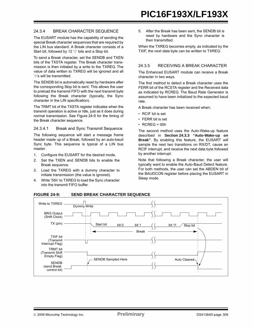
PIC16F193X/LF193X
24.3.4 BREAK CHARACTER SEQUENCE
The EUSART module has the capability of sending thespecial Break character sequences that are required bythe LIN bus standard. A Break character consists of aStart bit, followed by 12 ‘0’ bits and a Stop bit.
To send a Break character, set the SENDB and TXENbits of the TXSTA register. The Break character trans-mission is then initiated by a write to the TXREG. Thevalue of data written to TXREG will be ignored and all‘0’s will be transmitted.
The SENDB bit is automatically reset by hardware afterthe corresponding Stop bit is sent. This allows the userto preload the transmit FIFO with the next transmit bytefollowing the Break character (typically, the Synccharacter in the LIN specification).
The TRMT bit of the TXSTA register indicates when thetransmit operation is active or Idle, just as it does duringnormal transmission. See Figure 24-9 for the timing ofthe Break character sequence.
24.3.4.1 Break and Sync Transmit Sequence
The following sequence will start a message frameheader made up of a Break, followed by an auto-baudSync byte. This sequence is typical of a LIN busmaster.
1. Configure the EUSART for the desired mode.
2. Set the TXEN and SENDB bits to enable theBreak sequence.
3. Load the TXREG with a dummy character toinitiate transmission (the value is ignored).
4. Write ‘55h’ to TXREG to load the Sync characterinto the transmit FIFO buffer.
5. After the Break has been sent, the SENDB bit isreset by hardware and the Sync character isthen transmitted.
When the TXREG becomes empty, as indicated by theTXIF, the next data byte can be written to TXREG.
24.3.5 RECEIVING A BREAK CHARACTER
The Enhanced EUSART module can receive a Breakcharacter in two ways.
The first method to detect a Break character uses theFERR bit of the RCSTA register and the Received dataas indicated by RCREG. The Baud Rate Generator isassumed to have been initialized to the expected baudrate.
A Break character has been received when;
• RCIF bit is set
• FERR bit is set
• RCREG = 00h
The second method uses the Auto-Wake-up featuredescribed in Section 24.3.3 “Auto-Wake-up onBreak”. By enabling this feature, the EUSART willsample the next two transitions on RX/DT, cause anRCIF interrupt, and receive the next data byte followedby another interrupt.
Note that following a Break character, the user willtypically want to enable the Auto-Baud Detect feature.For both methods, the user can set the ABDEN bit ofthe BAUDCON register before placing the EUSART inSleep mode.
FIGURE 24-9: SEND BREAK CHARACTER SEQUENCE
Write to TXREGDummy Write
BRG Output(Shift Clock)
Start bit bit 0 bit 1 bit 11 Stop bit
Break
TXIF bit(Transmit
Interrupt Flag)
TX (pin)
TRMT bit(Transmit Shift
Empty Flag)
SENDB(send Break
control bit)
SENDB Sampled Here Auto Cleared
2009 Microchip Technology Inc. Preliminary DS41364D-page 309
PIC16F193X/LF193X
24.4 EUSART Synchronous Mode
Synchronous serial communications are typically usedin systems with a single master and one or moreslaves. The master device contains the necessary cir-cuitry for baud rate generation and supplies the clockfor all devices in the system. Slave devices can takeadvantage of the master clock by eliminating the inter-nal clock generation circuitry.
There are two signal lines in Synchronous mode: a bidi-rectional data line and a clock line. Slaves use theexternal clock supplied by the master to shift the serialdata into and out of their respective receive and trans-mit shift registers. Since the data line is bidirectional,synchronous operation is half-duplex only. Half-duplexrefers to the fact that master and slave devices canreceive and transmit data but not both simultaneously.The EUSART can operate as either a master or slavedevice.
Start and Stop bits are not used in synchronous trans-missions.
24.4.1 SYNCHRONOUS MASTER MODE
The following bits are used to configure the EUSARTfor Synchronous Master operation:
• SYNC = 1
• CSRC = 1
• SREN = 0 (for transmit); SREN = 1 (for receive)
• CREN = 0 (for transmit); CREN = 1 (for receive)
• SPEN = 1
Setting the SYNC bit of the TXSTA register configuresthe device for synchronous operation. Setting the CSRCbit of the TXSTA register configures the device as amaster. Clearing the SREN and CREN bits of the RCSTAregister ensures that the device is in the Transmit mode,otherwise the device will be configured to receive. Settingthe SPEN bit of the RCSTA register enables theEUSART.
24.4.1.1 Master Clock
Synchronous data transfers use a separate clock line,which is synchronous with the data. A device config-ured as a master transmits the clock on the TX/CK line.The TX/CK pin output driver is automatically enabledwhen the EUSART is configured for synchronoustransmit or receive operation. Serial data bits changeon the leading edge to ensure they are valid at the trail-ing edge of each clock. One clock cycle is generatedfor each data bit. Only as many clock cycles are gener-ated as there are data bits.
24.4.1.2 Clock Polarity
A clock polarity option is provided for Microwirecompatibility. Clock polarity is selected with the SCKPbit of the BAUDCON register. Setting the SCKP bit setsthe clock Idle state as high. When the SCKP bit is set,the data changes on the falling edge of each clock.
Clearing the SCKP bit sets the Idle state as low. Whenthe SCKP bit is cleared, the data changes on the risingedge of each clock.
24.4.1.3 Synchronous Master Transmission
Data is transferred out of the device on the RX/DT pin.The RX/DT and TX/CK pin output drivers are automat-ically enabled when the EUSART is configured for syn-chronous master transmit operation.
A transmission is initiated by writing a character to theTXREG register. If the TSR still contains all or part of aprevious character the new character data is held in theTXREG until the last bit of the previous character hasbeen transmitted. If this is the first character, or the pre-vious character has been completely flushed from theTSR, the data in the TXREG is immediately transferredto the TSR. The transmission of the character com-mences immediately following the transfer of the datato the TSR from the TXREG.
Each data bit changes on the leading edge of the mas-ter clock and remains valid until the subsequent leadingclock edge.
24.4.1.4 Synchronous Master Transmission Set-up:
1. Initialize the SPBRGH, SPBRGL register pairand the BRGH and BRG16 bits to achieve thedesired baud rate (see Section 24.3 “EUSARTBaud Rate Generator (BRG)”).
2. Enable the synchronous master serial port bysetting bits SYNC, SPEN and CSRC.
3. Disable Receive mode by clearing bits SRENand CREN.
4. Enable Transmit mode by setting the TXEN bit.
5. If 9-bit transmission is desired, set the TX9 bit.
6. If interrupts are desired, set the TXIE bit of thePIE1 register and the GIE and PEIE bits of theINTCON register.
7. If 9-bit transmission is selected, the ninth bitshould be loaded in the TX9D bit.
8. Start transmission by loading data to the TXREGregister.
Note: The TSR register is not mapped in datamemory, so it is not available to the user.
DS41364D-page 310 Preliminary 2009 Microchip Technology Inc.

PIC16F193X/LF193X
FIGURE 24-10: SYNCHRONOUS TRANSMISSION
FIGURE 24-11: SYNCHRONOUS TRANSMISSION (THROUGH TXEN)
TABLE 24-7: SUMMARY OF REGISTERS ASSOCIATED WITH SYNCHRONOUS MASTER TRANSMISSION
Name Bit 7 Bit 6 Bit 5 Bit 4 Bit 3 Bit 2 Bit 1 Bit 0Register on Page
BAUDCON ABDOVF RCIDL — SCKP BRG16 — WUE ABDEN 300
INTCON GIE PEIE TMR0IE INTE IOCIE TMR0IF INTF IOCIF 99
PIE1 TMR1GIE ADIE RCIE TXIE SSPIE CCP1IE TMR2IE TMR1IE 100
PIR1 TMR1GIF ADIF RCIF TXIF SSPIF CCP1IF TMR2IF TMR1IF 103
RCSTA SPEN RX9 SREN CREN ADDEN FERR OERR RX9D 299
SPBRGL BRG<7:0> 301*
SPBRGH BRG<15:8> 301*
TRISC TRISC7 TRISC6 TRISC5 TRISC4 TRISC3 TRISC2 TRISC1 TRISC0 140
TXREG EUSART Transmit Data Register 291*
TXSTA CSRC TX9 TXEN SYNC SENDB BRGH TRMT TX9D 298
Legend: x = unknown, - = unimplemented read as ‘0’. Shaded cells are not used for Synchronous Master Transmission.* Page provides register information.
bit 0 bit 1 bit 7
Word 1
bit 2 bit 0 bit 1 bit 7RX/DT
Write toTXREG Reg
TXIF bit(Interrupt Flag)
TXEN bit‘1’ ‘1’
Word 2
TRMT bit
Write Word 1 Write Word 2
Note: Sync Master mode, SPBRGL = 0, continuous transmission of two 8-bit words.
pin
TX/CK pin
TX/CK pin
(SCKP = 0)
(SCKP = 1)
RX/DT pin
TX/CK pin
Write toTXREG reg
TXIF bit
TRMT bit
bit 0 bit 1 bit 2 bit 6 bit 7
TXEN bit
2009 Microchip Technology Inc. Preliminary DS41364D-page 311

PIC16F193X/LF193X
24.4.1.5 Synchronous Master Reception
Data is received at the RX/DT pin. The RX/DT pinoutput driver is automatically disabled when theEUSART is configured for synchronous master receiveoperation.
In Synchronous mode, reception is enabled by settingeither the Single Receive Enable bit (SREN of theRCSTA register) or the Continuous Receive Enable bit(CREN of the RCSTA register).
When SREN is set and CREN is clear, only as manyclock cycles are generated as there are data bits in asingle character. The SREN bit is automatically clearedat the completion of one character. When CREN is set,clocks are continuously generated until CREN iscleared. If CREN is cleared in the middle of a characterthe CK clock stops immediately and the partial charac-ter is discarded. If SREN and CREN are both set, thenSREN is cleared at the completion of the first characterand CREN takes precedence.
To initiate reception, set either SREN or CREN. Data issampled at the RX/DT pin on the trailing edge of theTX/CK clock pin and is shifted into the Receive ShiftRegister (RSR). When a complete character isreceived into the RSR, the RCIF bit is set and the char-acter is automatically transferred to the two characterreceive FIFO. The Least Significant eight bits of the topcharacter in the receive FIFO are available in RCREG.The RCIF bit remains set as long as there are unreadcharacters in the receive FIFO.
24.4.1.6 Slave Clock
Synchronous data transfers use a separate clock line,which is synchronous with the data. A device configuredas a slave receives the clock on the TX/CK line. TheTX/CK pin output driver is automatically disabled whenthe device is configured for synchronous slave transmitor receive operation. Serial data bits change on theleading edge to ensure they are valid at the trailing edgeof each clock. One data bit is transferred for each clockcycle. Only as many clock cycles should be received asthere are data bits.
24.4.1.7 Receive Overrun Error
The receive FIFO buffer can hold two characters. Anoverrun error will be generated if a third character, in itsentirety, is received before RCREG is read to accessthe FIFO. When this happens the OERR bit of theRCSTA register is set. Previous data in the FIFO willnot be overwritten. The two characters in the FIFObuffer can be read, however, no additional characterswill be received until the error is cleared. The OERR bitcan only be cleared by clearing the overrun condition.If the overrun error occurred when the SREN bit is setand CREN is clear then the error is cleared by readingRCREG. If the overrun occurred when the CREN bit is
set then the error condition is cleared by either clearingthe CREN bit of the RCSTA register or by clearing theSPEN bit which resets the EUSART.
24.4.1.8 Receiving 9-bit Characters
The EUSART supports 9-bit character reception. Whenthe RX9 bit of the RCSTA register is set the EUSARTwill shift 9-bits into the RSR for each characterreceived. The RX9D bit of the RCSTA register is theninth, and Most Significant, data bit of the top unreadcharacter in the receive FIFO. When reading 9-bit datafrom the receive FIFO buffer, the RX9D data bit mustbe read before reading the 8 Least Significant bits fromthe RCREG.
24.4.1.9 Synchronous Master Reception Set-up:
1. Initialize the SPBRGH, SPBRGL register pair forthe appropriate baud rate. Set or clear theBRGH and BRG16 bits, as required, to achievethe desired baud rate.
2. Clear the ANSEL bit for the RX pin (if applicable).
3. Enable the synchronous master serial port bysetting bits SYNC, SPEN and CSRC.
4. Ensure bits CREN and SREN are clear.
5. If interrupts are desired, set the RCIE bit of thePIE1 register and the GIE and PEIE bits of theINTCON register.
6. If 9-bit reception is desired, set bit RX9.
7. Start reception by setting the SREN bit or forcontinuous reception, set the CREN bit.
8. Interrupt flag bit RCIF will be set when receptionof a character is complete. An interrupt will begenerated if the enable bit RCIE was set.
9. Read the RCSTA register to get the ninth bit (ifenabled) and determine if any error occurredduring reception.
10. Read the 8-bit received data by reading theRCREG register.
11. If an overrun error occurs, clear the error byeither clearing the CREN bit of the RCSTAregister or by clearing the SPEN bit which resetsthe EUSART.
DS41364D-page 312 Preliminary 2009 Microchip Technology Inc.
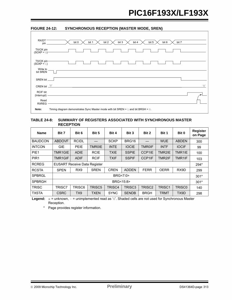
PIC16F193X/LF193X
FIGURE 24-12: SYNCHRONOUS RECEPTION (MASTER MODE, SREN)
TABLE 24-8: SUMMARY OF REGISTERS ASSOCIATED WITH SYNCHRONOUS MASTER RECEPTION
Name Bit 7 Bit 6 Bit 5 Bit 4 Bit 3 Bit 2 Bit 1 Bit 0Register on Page
BAUDCON ABDOVF RCIDL — SCKP BRG16 — WUE ABDEN 300
INTCON GIE PEIE TMR0IE INTE IOCIE TMR0IF INTF IOCIF 99
PIE1 TMR1GIE ADIE RCIE TXIE SSPIE CCP1IE TMR2IE TMR1IE 100
PIR1 TMR1GIF ADIF RCIF TXIF SSPIF CCP1IF TMR2IF TMR1IF 103
RCREG EUSART Receive Data Register 294*
RCSTA SPEN RX9 SREN CREN ADDEN FERR OERR RX9D 299
SPBRGL BRG<7:0> 301*
SPBRGH BRG<15:8> 301*
TRISC TRISC7 TRISC6 TRISC5 TRISC4 TRISC3 TRISC2 TRISC1 TRISC0 140
TXSTA CSRC TX9 TXEN SYNC SENDB BRGH TRMT TX9D 298
Legend: x = unknown, - = unimplemented read as ‘0’. Shaded cells are not used for Synchronous Master Reception.
* Page provides register information.
CREN bit
RX/DT
Write tobit SREN
SREN bit
RCIF bit(Interrupt)
ReadRXREG
‘0’
bit 0 bit 1 bit 2 bit 3 bit 4 bit 5 bit 6 bit 7
‘0’
Note: Timing diagram demonstrates Sync Master mode with bit SREN = 1 and bit BRGH = 0.
TX/CK pin
TX/CK pin
pin
(SCKP = 0)
(SCKP = 1)
2009 Microchip Technology Inc. Preliminary DS41364D-page 313

PIC16F193X/LF193X
24.4.2 SYNCHRONOUS SLAVE MODE
The following bits are used to configure the EUSARTfor Synchronous slave operation:
• SYNC = 1
• CSRC = 0
• SREN = 0 (for transmit); SREN = 1 (for receive)
• CREN = 0 (for transmit); CREN = 1 (for receive)
• SPEN = 1
Setting the SYNC bit of the TXSTA register configures thedevice for synchronous operation. Clearing the CSRC bitof the TXSTA register configures the device as a slave.Clearing the SREN and CREN bits of the RCSTA registerensures that the device is in the Transmit mode,otherwise the device will be configured to receive. Settingthe SPEN bit of the RCSTA register enables theEUSART.
24.4.2.1 EUSART Synchronous Slave Transmit
The operation of the Synchronous Master and Slavemodes are identical (see Section 24.4.1.3“Synchronous Master Transmission”), except in thecase of the Sleep mode.
If two words are written to the TXREG and then theSLEEP instruction is executed, the following will occur:
1. The first character will immediately transfer tothe TSR register and transmit.
2. The second word will remain in TXREG register.
3. The TXIF bit will not be set.
4. After the first character has been shifted out ofTSR, the TXREG register will transfer the secondcharacter to the TSR and the TXIF bit will now beset.
5. If the PEIE and TXIE bits are set, the interruptwill wake the device from Sleep and execute thenext instruction. If the GIE bit is also set, theprogram will call the Interrupt Service Routine.
24.4.2.2 Synchronous Slave Transmission Set-up:
1. Set the SYNC and SPEN bits and clear theCSRC bit.
2. Clear the ANSEL bit for the RX pin (if applicable).
3. Clear the CREN and SREN bits.
4. If interrupts are desired, set the TXIE bit of thePIE1 register and the GIE and PEIE bits of theINTCON register.
5. If 9-bit transmission is desired, set the TX9 bit.
6. Enable transmission by setting the TXEN bit.
7. If 9-bit transmission is selected, insert the MostSignificant bit into the TX9D bit.
8. Start transmission by writing the LeastSignificant 8 bits to the TXREG register.
TABLE 24-9: SUMMARY OF REGISTERS ASSOCIATED WITH SYNCHRONOUS SLAVE TRANSMISSION
Name Bit 7 Bit 6 Bit 5 Bit 4 Bit 3 Bit 2 Bit 1 Bit 0Register on Page
BAUDCON ABDOVF RCIDL — SCKP BRG16 — WUE ABDEN 300
INTCON GIE PEIE TMR0IE INTE IOCIE TMR0IF INTF IOCIF 99
PIE1 TMR1GIE ADIE RCIE TXIE SSPIE CCP1IE TMR2IE TMR1IE 100
PIR1 TMR1GIF ADIF RCIF TXIF SSPIF CCP1IF TMR2IF TMR1IF 103
RCSTA SPEN RX9 SREN CREN ADDEN FERR OERR RX9D 299
TRISC TRISC7 TRISC6 TRISC5 TRISC4 TRISC3 TRISC2 TRISC1 TRISC0 140
TXREG EUSART Transmit Data Register 291*
TXSTA CSRC TX9 TXEN SYNC SENDB BRGH TRMT TX9D 298
Legend: - = unimplemented read as ‘0’. Shaded cells are not used for Synchronous Slave Transmission.
* Page provides register information.
DS41364D-page 314 Preliminary 2009 Microchip Technology Inc.

PIC16F193X/LF193X
24.4.2.3 EUSART Synchronous Slave Reception
The operation of the Synchronous Master and Slavemodes is identical (Section 24.4.1.5 “SynchronousMaster Reception”), with the following exceptions:
• Sleep
• CREN bit is always set, therefore the receiver is never Idle
• SREN bit, which is a “don’t care” in Slave mode
A character may be received while in Sleep mode bysetting the CREN bit prior to entering Sleep. Once theword is received, the RSR register will transfer the datato the RCREG register. If the RCIE enable bit is set, theinterrupt generated will wake the device from Sleepand execute the next instruction. If the GIE bit is alsoset, the program will branch to the interrupt vector.
24.4.2.4 Synchronous Slave Reception Set-up:
1. Set the SYNC and SPEN bits and clear theCSRC bit.
2. Clear the ANSEL bit for both the CK and DT pins(if applicable).
3. If interrupts are desired, set the RCIE bit of thePIE1 register and the GIE and PEIE bits of theINTCON register.
4. If 9-bit reception is desired, set the RX9 bit.
5. Set the CREN bit to enable reception.
6. The RCIF bit will be set when reception iscomplete. An interrupt will be generated if theRCIE bit was set.
7. If 9-bit mode is enabled, retrieve the MostSignificant bit from the RX9D bit of the RCSTAregister.
8. Retrieve the 8 Least Significant bits from thereceive FIFO by reading the RCREG register.
9. If an overrun error occurs, clear the error byeither clearing the CREN bit of the RCSTAregister or by clearing the SPEN bit which resetsthe EUSART.
TABLE 24-10: SUMMARY OF REGISTERS ASSOCIATED WITH SYNCHRONOUS SLAVE RECEPTION
Name Bit 7 Bit 6 Bit 5 Bit 4 Bit 3 Bit 2 Bit 1 Bit 0Register on Page
BAUDCON ABDOVF RCIDL — SCKP BRG16 — WUE ABDEN 300
INTCON GIE PEIE TMR0IE INTE IOCIE TMR0IF INTF IOCIF 99
PIE1 TMR1GIE ADIE RCIE TXIE SSPIE CCP1IE TMR2IE TMR1IE 100
PIR1 TMR1GIF ADIF RCIF TXIF SSPIF CCP1IF TMR2IF TMR1IF 103
RCREG EUSART Receive Data Register 294*
RCSTA SPEN RX9 SREN CREN ADDEN FERR OERR RX9D 299
TRISC TRISC7 TRISC6 TRISC5 TRISC4 TRISC3 TRISC2 TRISC1 TRISC0 140
TXSTA CSRC TX9 TXEN SYNC SENDB BRGH TRMT TX9D 298
Legend: x = unknown, - = unimplemented read as ‘0’. Shaded cells are not used for Synchronous Slave Reception.
* Page provides register information.
2009 Microchip Technology Inc. Preliminary DS41364D-page 315
PIC16F193X/LF193X
24.5 EUSART Operation During Sleep
The EUSART will remain active during Sleep only in theSynchronous Slave mode. All other modes require thesystem clock and therefore cannot generate the neces-sary signals to run the Transmit or Receive Shift regis-ters during Sleep.
Synchronous Slave mode uses an externally generatedclock to run the Transmit and Receive Shift registers.
24.5.1 SYNCHRONOUS RECEIVE DURING SLEEP
To receive during Sleep, all the following conditionsmust be met before entering Sleep mode:
• RCSTA and TXSTA Control registers must be configured for Synchronous Slave Reception (see Section 24.4.2.4 “Synchronous Slave Reception Set-up:”).
• If interrupts are desired, set the RCIE bit of the PIE1 register and the GIE and PEIE bits of the INTCON register.
• The RCIF interrupt flag must be cleared by read-ing RCREG to unload any pending characters in the receive buffer.
Upon entering Sleep mode, the device will be ready toaccept data and clocks on the RX/DT and TX/CK pins,respectively. When the data word has been completelyclocked in by the external device, the RCIF interruptflag bit of the PIR1 register will be set. Thereby, wakingthe processor from Sleep.
Upon waking from Sleep, the instruction following theSLEEP instruction will be executed. If the GIE globalinterrupt enable bit of the INTCON register is also set,then the Interrupt Service Routine at address 004h willbe called.
24.5.2 SYNCHRONOUS TRANSMIT DURING SLEEP
To transmit during Sleep, all the following conditionsmust be met before entering Sleep mode:
• RCSTA and TXSTA Control registers must be configured for Synchronous Slave Transmission (see Section 24.4.2.2 “Synchronous Slave Transmission Set-up:”).
• The TXIF interrupt flag must be cleared by writing the output data to the TXREG, thereby filling the TSR and transmit buffer.
• If interrupts are desired, set the TXIE bit of the PIE1 register and the PEIE bit of the INTCON reg-ister.
• Interrupt enable bits TXIE of the PIE1 register and PEIE of the INTCON register must set.
Upon entering Sleep mode, the device will be ready toaccept clocks on TX/CK pin and transmit data on theRX/DT pin. When the data word in the TSR has beencompletely clocked out by the external device, thepending byte in the TXREG will transfer to the TSR andthe TXIF flag will be set. Thereby, waking the processorfrom Sleep. At this point, the TXREG is available toaccept another character for transmission, which willclear the TXIF flag.
Upon waking from Sleep, the instruction following theSLEEP instruction will be executed. If the GlobalInterrupt Enable (GIE) bit is also set then the InterruptService Routine at address 0004h will be called.
DS41364D-page 316 Preliminary 2009 Microchip Technology Inc.

PIC16F193X/LF193X
25.0 CAPACITIVE SENSING MODULE
The capacitive sensing module allows for an interactionwith an end user without a mechanical interface. In atypical application, the capacitive sensing module isattached to a pad on a Printed Circuit Board (PCB),which is electrically isolated from the end user. When theend user places their finger over the PCB pad, acapacitive load is added, causing a frequency shift in thecapacitive sensing module. The capacitive sensingmodule requires software and at least one timerresource to determine the change in frequency. Keyfeatures of this module include:
• Analog MUX for monitoring multiple inputs
• Capacitive sensing oscillator
• Multiple Power modes
• High power range with variable voltage references (PIC16F/LF1933/1938/1939 only)
• Multiple timer resources
• Software control
• Operation during Sleep
FIGURE 25-1: CAPACITIVE SENSING BLOCK DIAGRAM
TMR0CS
CPS0
CPS1
CPS2
CPS3
CPS4
CPS5
CPS6
CPS7
CPS8(1)
CPS9(1)
CPS10(1)
CPSCH<3:0>(2)
Capacitive Sensing
Oscillator
CPSOSC
CPSON
CPSRNG<1:0>
TMR00
1
SetTMR0IF
Overflow
T0XCS
0
1
T0CKI
CPSOUT
CPS11(1)
CPS12(1)
CPS13(1)
CPS14(1)
CPS15(1)
CPSCLK
Note 1: Reference CPSCON1 register (Register 25-2) for channels implemented on each device.2: CPSCH3 is not implemented on PIC16F1933/1936/1938/PIC16LF1933/1936/1938.3: If CPSON = 0, disabling capacitive sensing, no channel is selected.4: Variable Voltage Reference selection is implemented on PIC16F/LF1934/1936/1937 only.
FOSC/4
Timer0 Module
CPSON(3)
T1CS<1:0>
T1OSC/T1CKI
TMR1H:TMR1LEN
T1GSEL<1:0>
Timer1 GateControl Logic
T1G
FOSC
FOSC/4
Timer1 Module
SYNCC1OUT
SYNCC2OUT
0
1
Int.Ref.
FVR(4)
DAC(4)
Ref+
Ref-
CPSRM(4)
0
1
2009 Microchip Technology Inc. Preliminary DS41364D-page 317

PIC16F193X/LF193X
FIGURE 25-2: CAPACITIVE SENSING OSCILLATOR BLOCK DIAGRAM
0
1
VDD
CPSCLK
Oscillator Module
CPSxS Q
R
+
-
+
-
Note 1: Module Enable and Power mode selections are not shown.2: Comparators remain active in Noise Detection mode on PIC16F/LF1933/1938/1939 only.3: Variable Voltage Reference selection is implemented on PIC16F/LF1933/1938/1939 only.
(2)(1)
(1) (2)
0
1
InternalReferences
FVR(3)DAC(3)
CPSRM(3)
Analog Pin
Ref- Ref+
DS41364D-page 318 Preliminary 2009 Microchip Technology Inc.
PIC16F193X/LF193X
25.1 Analog MUX
The capacitive sensing module can monitor up to 16inputs. The capacitive sensing inputs are defined asCPS<15:0>. To determine if a frequency change hasoccurred the user must:
• Select the appropriate CPS pin by setting the CPSCH<3:0> bits of the CPSCON1 register.
• Set the corresponding ANSEL bit.
• Set the corresponding TRIS bit.
• Run the software algorithm.
Selection of the CPSx pin while the module is enabledwill cause the capacitive sensing oscillator to be on theCPSx pin. Failure to set the corresponding ANSEL andTRIS bits can cause the capacitive sensing oscillator tostop, leading to false frequency readings.
25.2 Capacitive Sensing Oscillator
The capacitive sensing oscillator consists of a constantcurrent source and a constant current sink, to producea triangle waveform. The CPSOUT bit of theCPSCON0 register shows the status of the capacitivesensing oscillator, whether it is a sinking or sourcingcurrent. The oscillator is designed to drive a capacitiveload (single PCB pad) and at the same time, be a clocksource to either Timer0 or Timer1. The oscillator hasthree different current settings as defined byCPSRNG<1:0> of the CPSCON0 register. The differentcurrent settings for the oscillator serve two purposes:
• Maximize the number of counts in a timer for a fixed time base.
• Maximize the count differential in the timer during a change in frequency.
25.3 Voltage References
The capacitive sensing oscillator uses voltage refer-ences to provide two voltage thresholds for oscillation.The upper voltage threshold is referred to as Ref+ andthe lower voltage threshold is referred to as Ref-.
The user can elect to use fixed voltage references,which are internal to the capacitive sensing oscillator,or variable voltage references, which are supplied bythe Fixed Voltage Reference (FVR) module and theDigital-to-Analog Converter (DAC) module.
When the fixed voltage references are used, the VSS
voltage determines the lower threshold level (Ref-) andthe VDD voltage determines the upper threshold level(Ref+).
When the variable voltage references are used, theDAC voltage determines the lower threshold level(Ref-) and the FVR voltage determines the upperthreshold level (Ref+). An advantage of using these ref-erence sources is that oscillation frequency remainsconstant with changes in VDD.
Different oscillation frequencies can be obtainedthrough the use of these variable voltage references.The more the upper voltage reference level is loweredand the more the lower voltage reference level israised, the higher the capacitive sensing oscillator fre-quency becomes.
Selection between the voltage references is controlledby the CPSRM bit of the CPSCON0 register. Settingthis bit selects the variable voltage references andclearing this bit selects the fixed voltage references.
Please see Section 14.0 “Fixed Voltage Reference(FVR)” and Section 16.0 “Digital-to-Analog Con-verter (DAC) Module” for more information on config-uring the variable voltage levels.
Note: The variable Voltage References featureis only available on thePIC16F/LF1933/1938/1939 devices.
2009 Microchip Technology Inc. Preliminary DS41364D-page 319
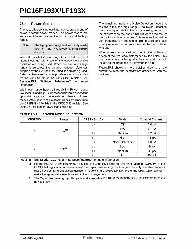
PIC16F193X/LF193X
25.4 Power Modes
The capacitive sensing oscillator can operate in one ofseven different power modes. The power modes areseparated into two ranges; the low range and the highrange.
When the oscillator’s low range is selected, the fixedinternal voltage references of the capacitive sensingoscillator are being used. When the oscillator’s highrange is selected, the variable voltage referencessupplied by the FVR and DAC modules are being used.Selection between the voltage references is controlledby the CPSRM bit of the CPSCON0 register. SeeSection 25.3 “Voltage References” for moreinformation.
Within each range there are three distinct Power modes;low, medium and high. Current consumption is dependentupon the range and mode selected. Selecting Powermodes within each range is accomplished by configuringthe CPSRNG <1:0> bits in the CPSCON0 register. SeeTable 25-1 for proper Power mode selection.
The remaining mode is a Noise Detection mode thatresides within the high range. The Noise Detectionmode is unique in that it disables the sinking and sourc-ing of current on the analog pin but leaves the rest ofthe oscillator circuitry active. This reduces the oscilla-tion frequency on the analog pin to zero and alsogreatly reduces the current consumed by the oscillatormodule.
When noise is introduced onto the pin, the oscillator isdriven at the frequency determined by the noise. Thisproduces a detectable signal at the comparator output,indicating the presence of activity on the pin.
Figure 25-2 shows a more detailed drawing of thecurrent sources and comparators associated with theoscillator.
TABLE 25-1: POWER MODE SELECTION
Note: The high power range feature is only avail-able on the PIC16F/LF1933/1938/1939devices.
CPSRM(2) Range CPSRNG<1:0> Mode Nominal Current(1)
0 Low(2)
00 Off 0.0 A
01 Low 0.1 A
10 Medium 1.2 A
11 High 18 A
1 High(3)
00 Noise Detection 0.0 A
01 Low 9 A
10 Medium 30 A
11 High 100 A
Note 1: See Section 29.0 “Electrical Specifications” for more information.
2: For the PIC16F/LF1934/1936/1937 devices, the Capacitive Sensing Reference Mode bit (CPSRM) of the CPSCON0 register is not available and the Capacitive Sensing Low Range is the only operable range for these devices. Different bit configurations made with the CPSRNG<1:0> bits of the CPSCON0 register make the appropriate selections within the low range only.
3: The Capacitive Sensing High Range is available on the PIC16F1933/1938/1939/PIC16LF1933/1938/1939 devices only.
DS41364D-page 320 Preliminary 2009 Microchip Technology Inc.
PIC16F193X/LF193X
25.5 Timer Resources
To measure the change in frequency of the capacitivesensing oscillator, a fixed time base is required. For theperiod of the fixed time base, the capacitive sensingoscillator is used to clock either Timer0 or Timer1. Thefrequency of the capacitive sensing oscillator is equalto the number of counts in the timer divided by theperiod of the fixed time base.
25.6 Fixed Time Base
To measure the frequency of the capacitive sensingoscillator, a fixed time base is required. Any timerresource or software loop can be used to establish thefixed time base. It is up to the end user to determine themethod in which the fixed time base is generated.
25.6.1 TIMER0
To select Timer0 as the timer resource for the capacitivesensing module:
• Set the T0XCS bit of the CPSCON0 register.
• Clear the TMR0CS bit of the OPTION register.
When Timer0 is chosen as the timer resource, thecapacitive sensing oscillator will be the clock source forTimer0. Refer to Section 19.0 “Timer0 Module” foradditional information.
25.6.2 TIMER1
To select Timer1 as the timer resource for thecapacitive sensing module, set the TMR1CS<1:0> ofthe T1CON register to ‘11’. When Timer1 is chosen asthe timer resource, the capacitive sensing oscillator willbe the clock source for Timer1. Because the Timer1module has a gate control, developing a time base forthe frequency measurement can be simplified by usingthe Timer0 overflow flag.
It is recommend that the Timer0 overflow flag, in con-junction with the Toggle mode of the Timer1 Gate, beused to develop the fixed time base required by thesoftware portion of the capacitive sensing module.Refer to Section 20.12 “Timer1 Gate Control Regis-ter” for additional information.
TABLE 25-2: TIMER1 ENABLE FUNCTION
25.7 Software Control
The software portion of the capacitive sensing moduleis required to determine the change in frequency of thecapacitive sensing oscillator. This is accomplished bythe following:
• Setting a fixed time base to acquire counts on Timer0 or Timer1.
• Establishing the nominal frequency for the capacitive sensing oscillator.
• Establishing the reduced frequency for the capacitive sensing oscillator due to an additional capacitive load.
• Set the frequency threshold.
25.7.1 NOMINAL FREQUENCY(NO CAPACITIVE LOAD)
To determine the nominal frequency of the capacitivesensing oscillator:
• Remove any extra capacitive load on the selected CPSx pin.
• At the start of the fixed time base, clear the timer resource.
• At the end of the fixed time base save the value in the timer resource.
The value of the timer resource is the number ofoscillations of the capacitive sensing oscillator for thegiven time base. The frequency of the capacitivesensing oscillator is equal to the number of counts onin the timer divided by the period of the fixed time base.
25.7.2 REDUCED FREQUENCY (ADDITIONAL CAPACITIVE LOAD)
The extra capacitive load will cause the frequency of thecapacitive sensing oscillator to decrease. To determinethe reduced frequency of the capacitive sensingoscillator:
• Add a typical capacitive load on the selected CPSx pin.
• Use the same fixed time base as the nominal frequency measurement.
• At the start of the fixed time base, clear the timer resource.
• At the end of the fixed time base save the value in the timer resource.
The value of the timer resource is the number of oscil-lations of the capacitive sensing oscillator with an addi-tional capacitive load. The frequency of the capacitivesensing oscillator is equal to the number of counts onin the timer divided by the period of the fixed time base.This frequency should be less than the value obtainedduring the nominal frequency measurement.
Note: The fixed time base can not be generatedby the timer resource that the capacitivesensing oscillator is clocking.
TMR1ON TMR1GE Timer1 Operation
0 0 Off
0 1 Off
1 0 On
1 1 Count Enabled by input
2009 Microchip Technology Inc. Preliminary DS41364D-page 321
PIC16F193X/LF193X
25.7.3 FREQUENCY THRESHOLD
The frequency threshold should be placed midwaybetween the value of nominal frequency and thereduced frequency of the capacitive sensing oscillator.Refer to Application Note AN1103, “Software Handlingfor Capacitive Sensing” (DS01103) for more detailedinformation on the software required for capacitivesensing module.
25.8 Operation during Sleep
The capacitive sensing oscillator will continue to run aslong as the module is enabled, independent of the partbeing in Sleep. In order for the software to determine ifa frequency change has occurred, the part must beawake. However, the part does not have to be awakewhen the timer resource is acquiring counts.
Note: For more information on general capacitivesensing refer to Application Notes:
• AN1101, “Introduction to Capacitive Sensing” (DS01101)
• AN1102, “Layout and Physical Design Guidelines for Capacitive Sensing” (DS01102)
Note: Timer0 does not operate when in Sleep,and therefore cannot be used forcapacitive sense measurements in Sleep.
DS41364D-page 322 Preliminary 2009 Microchip Technology Inc.

PIC16F193X/LF193X
REGISTER 25-1: CPSCON0: CAPACITIVE SENSING CONTROL REGISTER 0
R/W-0/0 R/W-0/0 U-0 U-0 R/W-0/0 R/W-0/0 R-0/0 R/W-0/0
CPSON CPSRM(1) — — CPSRNG<1:0> CPSOUT T0XCS
bit 7 bit 0
Legend:
R = Readable bit W = Writable bit U = Unimplemented bit, read as ‘0’
u = Bit is unchanged x = Bit is unknown -n/n = Value at POR and BOR/Value at all other Resets
‘1’ = Bit is set ‘0’ = Bit is cleared
bit 7 CPSON: Capacitive Sensing Module Enable bit1 = Capacitive sensing module is enabled0 = Capacitive sensing module is disabled
bit 6 CPSRM: Capacitive Sensing Reference Mode bit(1)
1 = Capacitive Sensing module is in high range. DAC and FVR provide oscillator voltage references.0 = Capacitive Sensing module is in the low range. Internal oscillator voltage references are used.
bit 5-4 Unimplemented: Read as ‘0’
bit 3-2 CPSRNG<1:0>: Capacitive Sensing Current RangeIf CPSRM = 0 (low range):(1)
00 = Oscillator is off01 = Oscillator is in Low Range. Charge/Discharge Current is nominally 0.1 µA10 = Oscillator is in Medium Range. Charge/Discharge Current is nominally 1.2 µA11 = Oscillator is in High Range. Charge/Discharge Current is nominally 18 µA
If CPSRM = 1 (high range):(2)
00 = Oscillator is on. Noise Detection mode. No Charge/Discharge current is supplied.01 = Oscillator is in Low Range. Charge/Discharge Current is nominally 9 µA10 = Oscillator is in Medium Range. Charge/Discharge Current is nominally 30 µA11 = Oscillator is in High Range. Charge/Discharge Current is nominally 100 µA
bit 1 CPSOUT: Capacitive Sensing Oscillator Status bit1 = Oscillator is sourcing current (Current flowing out of the pin)0 = Oscillator is sinking current (Current flowing into the pin)
bit 0 T0XCS: Timer0 External Clock Source Select bitIf TMR0CS = 1: The T0XCS bit controls which clock external to the core/Timer0 module supplies Timer0:1 = Timer0 clock source is the capacitive sensing oscillator0 = Timer0 clock source is the T0CKI pinIf TMR0CS = 0:Timer0 clock source is controlled by the core/Timer0 module and is FOSC/4
Note 1: For the PIC16F/LF1934/1936/1937 devices, the Capacitive Sensing Reference Mode bit (CPSRM) is not available and the Capacitive Sensing Low Range is the only operable range for these devices. Different bit configurations made with the CPSRNG<1:0> bits of the CPSCON0 register make the appropriate selections within the low range only.
2: The Capacitive Sensing High Range is available on the PIC16F/LF1933/1938/1939 devices only.
2009 Microchip Technology Inc. Preliminary DS41364D-page 323
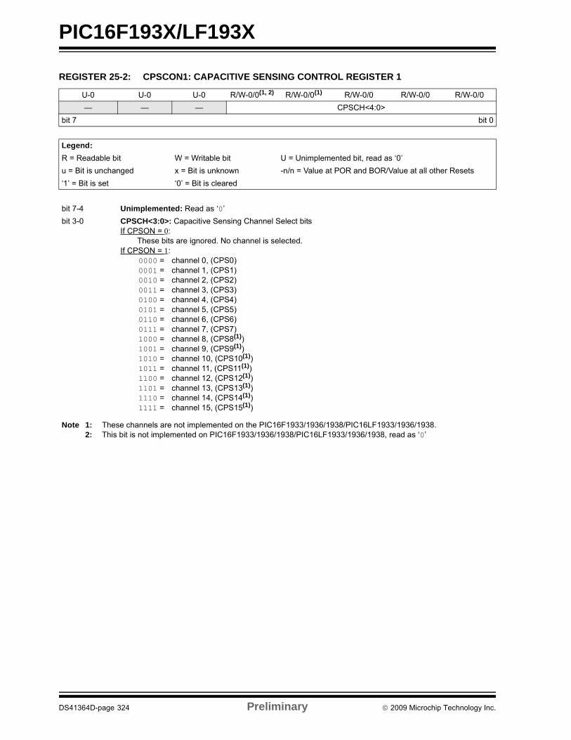
PIC16F193X/LF193X
REGISTER 25-2: CPSCON1: CAPACITIVE SENSING CONTROL REGISTER 1
U-0 U-0 U-0 R/W-0/0(1, 2) R/W-0/0(1) R/W-0/0 R/W-0/0 R/W-0/0
— — — CPSCH<4:0>
bit 7 bit 0
Legend:
R = Readable bit W = Writable bit U = Unimplemented bit, read as ‘0’
u = Bit is unchanged x = Bit is unknown -n/n = Value at POR and BOR/Value at all other Resets
‘1’ = Bit is set ‘0’ = Bit is cleared
bit 7-4 Unimplemented: Read as ‘0’
bit 3-0 CPSCH<3:0>: Capacitive Sensing Channel Select bitsIf CPSON = 0:
These bits are ignored. No channel is selected.If CPSON = 1:
0000 = channel 0, (CPS0)0001 = channel 1, (CPS1)0010 = channel 2, (CPS2)0011 = channel 3, (CPS3)0100 = channel 4, (CPS4)0101 = channel 5, (CPS5)0110 = channel 6, (CPS6)0111 = channel 7, (CPS7)1000 = channel 8, (CPS8(1))1001 = channel 9, (CPS9(1))1010 = channel 10, (CPS10(1))1011 = channel 11, (CPS11(1))1100 = channel 12, (CPS12(1))1101 = channel 13, (CPS13(1))1110 = channel 14, (CPS14(1))1111 = channel 15, (CPS15(1))
Note 1: These channels are not implemented on the PIC16F1933/1936/1938/PIC16LF1933/1936/1938.2: This bit is not implemented on PIC16F1933/1936/1938/PIC16LF1933/1936/1938, read as ‘0’
DS41364D-page 324 Preliminary 2009 Microchip Technology Inc.
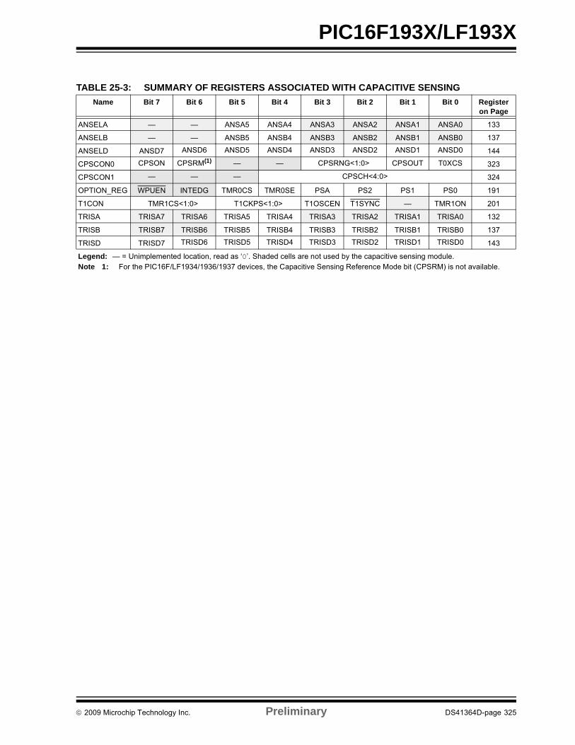
PIC16F193X/LF193X
TABLE 25-3: SUMMARY OF REGISTERS ASSOCIATED WITH CAPACITIVE SENSING Name Bit 7 Bit 6 Bit 5 Bit 4 Bit 3 Bit 2 Bit 1 Bit 0 Register
on Page
ANSELA — — ANSA5 ANSA4 ANSA3 ANSA2 ANSA1 ANSA0 133
ANSELB — — ANSB5 ANSB4 ANSB3 ANSB2 ANSB1 ANSB0 137
ANSELD ANSD7 ANSD6 ANSD5 ANSD4 ANSD3 ANSD2 ANSD1 ANSD0 144
CPSCON0 CPSON CPSRM(1) — — CPSRNG<1:0> CPSOUT T0XCS 323
CPSCON1 — — — CPSCH<4:0> 324
OPTION_REG WPUEN INTEDG TMR0CS TMR0SE PSA PS2 PS1 PS0 191
T1CON TMR1CS<1:0> T1CKPS<1:0> T1OSCEN T1SYNC — TMR1ON 201
TRISA TRISA7 TRISA6 TRISA5 TRISA4 TRISA3 TRISA2 TRISA1 TRISA0 132
TRISB TRISB7 TRISB6 TRISB5 TRISB4 TRISB3 TRISB2 TRISB1 TRISB0 137
TRISD TRISD7 TRISD6 TRISD5 TRISD4 TRISD3 TRISD2 TRISD1 TRISD0 143
Legend: — = Unimplemented location, read as ‘0’. Shaded cells are not used by the capacitive sensing module.Note 1: For the PIC16F/LF1934/1936/1937 devices, the Capacitive Sensing Reference Mode bit (CPSRM) is not available.
2009 Microchip Technology Inc. Preliminary DS41364D-page 325

PIC16F193X/LF193X
NOTES:
DS41364D-page 326 Preliminary 2009 Microchip Technology Inc.

PIC16F193X/LF193X
26.0 LIQUID CRYSTAL DISPLAY (LCD) DRIVER MODULE
The Liquid Crystal Display (LCD) driver modulegenerates the timing control to drive a static ormultiplexed LCD panel. In the PIC16F193X/LF193Xdevice, the module drives the panels of up to fourcommons and up to 24 segments. The LCD modulealso provides control of the LCD pixel data.
The LCD driver module supports:
• Direct driving of LCD panel
• Three LCD clock sources with selectable prescaler
• Up to four common pins:
- Static (1 common)
- 1/2 multiplex (2 commons)
- 1/3 multiplex (3 commons)
- 1/4 multiplex (4 commons)
• Segment pins up to:
- 16 (PIC16F1933/1936/1938/PIC16LF1933/1936/1938)
- 24 (PIC16F1934/1937/1939/PIC16LF1934/1937/1939)
• Static, 1/2 or 1/3 LCD Bias
FIGURE 26-1: LCD DRIVER MODULE BLOCK DIAGRAM
Note: COM3 and SEG15 share the same physicalpin on the PIC16F1933/1936/1938/PIC16LF1933/1936/1938, therefore SEG15is not available when using 1/4 multiplexdisplays.
Data BusSEG<23:0>(1, 3)
To I/O Pads(1)LCDDATAx
Registers
Note 1: These are not directly connected to the I/O pads, but may be tri-stated, depending on the configuration of the LCD module.
2: SEG<23:0> on PIC16F1934/1937/1939, SEG<15:0> on PIC16F1933/1936/1938/ PIC16LF1933/1936/1938.
3: COM3 and SEG15 share the same physical pin on the PIC16F1933/1936/1938/PIC16LF1933/1936/1938, therefore SEG15 is not available when using 1/4 multiplex displays.
COM<3:0>(3)
Clock Source
Timing Control
Select andPrescaler
LFINTOSC
FOSC/256
T1OSC
To I/O Pads(1)
LCDCON
LCDPS
LCDSEn
MUX
2009 Microchip Technology Inc. Preliminary DS41364D-page 327

PIC16F193X/LF193X
26.1 LCD Registers
The module contains the following registers:
• LCD Control register (LCDCON)
• LCD Phase register (LCDPS)
• LCD Reference Ladder register (LCDRL)
• LCD Contrast Control register (LCDCST)
• LCD Reference Voltage Control register (LCDREF)
• Up to 3 LCD Segment Enable registers (LCDSEn)
• Up to 12 LCD data registers (LCDDATAn)
TABLE 26-1: LCD SEGMENT AND DATA REGISTERS
The LCDCON register (Register 26-1) controls theoperation of the LCD driver module. The LCDPS regis-ter (Register 26-2) configures the LCD clock sourceprescaler and the type of waveform; Type-A or Type-B.The LCDSEn registers (Register 26-5) configure thefunctions of the port pins.
The following LCDSEn registers are available:
• LCDSE0 SE<7:0>• LCDSE1 SE<15:8>• LCDSE2 SE<23:16>(1)
Once the module is initialized for the LCD panel, theindividual bits of the LCDDATAn registers arecleared/set to represent a clear/dark pixel, respectively:
• LCDDATA0 SEG<7:0>COM0• LCDDATA1 SEG<15:8>COM0• LCDDATA2 SEG<23:16>COM0(1)
• LCDDATA3 SEG<7:0>COM1• LCDDATA4 SEG<15:8>COM1• LCDDATA5 SEG<23:16>COM1(1)
• LCDDATA6 SEG<7:0>COM2• LCDDATA7 SEG<15:8>COM2• LCDDATA8 SEG<23:16>COM2(1)
• LCDDATA9 SEG<7:0>COM3• LCDDATA10 SEG<15:8>COM3• LCDDATA11 SEG<23:16>COM3(1)
As an example, LCDDATAn is detailed inRegister 26-6.
Once the module is configured, the LCDEN bit of theLCDCON register is used to enable or disable the LCDmodule. The LCD panel can also operate during Sleepby clearing the SLPEN bit of the LCDCON register.
Device# of LCD Registers
SegmentEnable
Data
PIC16F1933/1936/1938/PIC16LF1933/1936/1938
2 8
PIC16F1934/1937/1939/PIC16LF1934/1937/1939
3 12
Note 1: PIC16F1934/1937/1939/PIC16LF1934/1937/1939 only.
Note 1: PIC16F1934/1937/1939/PIC16LF1934/1937/1939 only.
DS41364D-page 328 Preliminary 2009 Microchip Technology Inc.
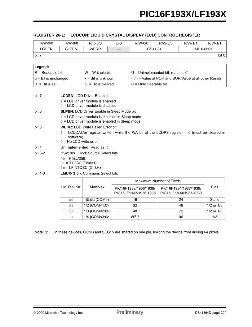
PIC16F193X/LF193X
REGISTER 26-1: LCDCON: LIQUID CRYSTAL DISPLAY (LCD) CONTROL REGISTER
R/W-0/0 R/W-0/0 R/C-0/0 U-0 R/W-0/0 R/W-0/0 R/W-1/1 R/W-1/1
LCDEN SLPEN WERR — CS<1:0> LMUX<1:0>
bit 7 bit 0
Legend:
R = Readable bit W = Writable bit U = Unimplemented bit, read as ‘0’
u = Bit is unchanged x = Bit is unknown -n/n = Value at POR and BOR/Value at all other Resets
‘1’ = Bit is set ‘0’ = Bit is cleared C = Only clearable bit
bit 7 LCDEN: LCD Driver Enable bit
1 = LCD driver module is enabled 0 = LCD driver module is disabled
bit 6 SLPEN: LCD Driver Enable in Sleep Mode bit
1 = LCD driver module is disabled in Sleep mode0 = LCD driver module is enabled in Sleep mode
bit 5 WERR: LCD Write Failed Error bit
1 = LCDDATAn register written while the WA bit of the LCDPS register = 0 (must be cleared insoftware)
0 = No LCD write error
bit 4 Unimplemented: Read as ‘0’
bit 3-2 CS<1:0>: Clock Source Select bits
00 = FOSC/25601 = T1OSC (Timer1)1x = LFINTOSC (31 kHz)
bit 1-0 LMUX<1:0>: Commons Select bits
Note 1: On these devices, COM3 and SEG15 are shared on one pin, limiting the device from driving 64 pixels.
LMUX<1:0> Multiplex
Maximum Number of Pixels
BiasPIC16F1933/1936/1938/PIC16LF1933/1936/1938
PIC16F1934/1937/1939/PIC16LF1934/1937/1939
00 Static (COM0) 16 24 Static
01 1/2 (COM<1:0>) 32 48 1/2 or 1/3
10 1/3 (COM<2:0>) 48 72 1/2 or 1/3
11 1/4 (COM<3:0>) 60(1) 96 1/3
2009 Microchip Technology Inc. Preliminary DS41364D-page 329

PIC16F193X/LF193X
REGISTER 26-2: LCDPS: LCD PHASE REGISTER
R/W-0/0 R/W-0/0 R-0/0 R-0/0 R/W-0/0 R/W-0/0 R/W-1/1 R/W-1/1
WFT BIASMD LCDA WA LP<3:0>
bit 7 bit 0
Legend:
R = Readable bit W = Writable bit U = Unimplemented bit, read as ‘0’
u = Bit is unchanged x = Bit is unknown -n/n = Value at POR and BOR/Value at all other Resets
‘1’ = Bit is set ‘0’ = Bit is cleared C = Only clearable bit
bit 7 WFT: Waveform Type bit
1 = Type-B phase changes on each frame boundary0 = Type-A phase changes within each common type
bit 6 BIASMD: Bias Mode Select bit
When LMUX<1:0> = 00:
0 = Static Bias mode (do not set this bit to ‘1’)When LMUX<1:0> = 01:
1 = 1/2 Bias mode0 = 1/3 Bias modeWhen LMUX<1:0> = 10:
1 = 1/2 Bias mode0 = 1/3 Bias modeWhen LMUX<1:0> = 11:
0 = 1/3 Bias mode (do not set this bit to ‘1’)
bit 5 LCDA: LCD Active Status bit
1 = LCD driver module is active0 = LCD driver module is inactive
bit 4 WA: LCD Write Allow Status bit
1 = Writing to the LCDDATAn registers is allowed0 = Writing to the LCDDATAn registers is not allowed
bit 3-0 LP<3:0>: LCD Prescaler Selection bits
1111 = 1:161110 = 1:151101 = 1:141100 = 1:131011 = 1:121010 = 1:111001 = 1:101000 = 1:90111 = 1:80110 = 1:70101 = 1:60100 = 1:50011 = 1:40010 = 1:30001 = 1:20000 = 1:1
DS41364D-page 330 Preliminary 2009 Microchip Technology Inc.

PIC16F193X/LF193X
REGISTER 26-3: LCDREF: LCD REFERENCE VOLTAGE CONTROL REGISTER
R/W-0/0 R/W-0/0 R/W-0/0 U-0 R/W-0/0 R/W-0/0 R/W-0/0 U-0
LCDIRE LCDIRS LCDIRI — VLCD3PE VLCD2PE VLCD1PE —
bit 7 bit 0
Legend:
R = Readable bit W = Writable bit U = Unimplemented bit, read as ‘0’
u = Bit is unchanged x = Bit is unknown -n/n = Value at POR and BOR/Value at all other Resets
‘1’ = Bit is set ‘0’ = Bit is cleared C = Only clearable bit
bit 7 LCDIRE: LCD Internal Reference Enable bit
1 = Internal LCD Reference is enabled and connected to the Internal Contrast Control circuit0 = Internal LCD Reference is disabled
bit 6 LCDIRS: LCD Internal Reference Source bit
If LCDIRE = 1:0 = Internal LCD Contrast Control is powered by VDD
1 = Internal LCD Contrast Control is powered by a 3.072V output of the FVR.If LCDIRE = 0:Internal LCD Contrast Control is unconnected. LCD bandgap buffer is disabled.
bit 5 LCDIRI: LCD Internal Reference Ladder Idle Enable bit
Allows the Internal FVR buffer to shut down when the LCD Reference Ladder is in power mode ‘B’1 = When the LCD Reference Ladder is in power mode ‘B’, the LCD Internal FVR buffer is disabled.0 = The LCD Internal FVR Buffer ignores the LCD Reference Ladder Power mode.
bit 4 Unimplemented: Read as ‘0’
bit 3 VLCD3PE: VLCD3 Pin Enable bit
1 = The VLCD3 pin is connected to the internal bias voltage LCDBIAS3(1)
0 = The VLCD3 pin is not connected
bit 2 VLCD2PE: VLCD2 Pin Enable bit
1 = The VLCD2 pin is connected to the internal bias voltage LCDBIAS2(1)
0 = The VLCD2 pin is not connected
bit 1 VLCD1PE: VLCD1 Pin Enable bit
1 = The VLCD1 pin is connected to the internal bias voltage LCDBIAS1(1)
0 = The VLCD1 pin is not connected
bit 0 Unimplemented: Read as ‘0’
Note 1: Normal pin controls of TRISx and ANSELx are unaffected.
2009 Microchip Technology Inc. Preliminary DS41364D-page 331
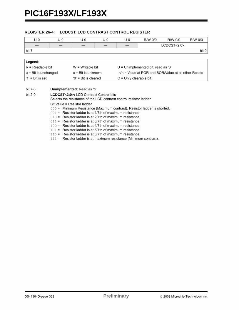
PIC16F193X/LF193X
REGISTER 26-4: LCDCST: LCD CONTRAST CONTROL REGISTER
U-0 U-0 U-0 U-0 U-0 R/W-0/0 R/W-0/0 R/W-0/0
— — — — — LCDCST<2:0>
bit 7 bit 0
Legend:
R = Readable bit W = Writable bit U = Unimplemented bit, read as ‘0’
u = Bit is unchanged x = Bit is unknown -n/n = Value at POR and BOR/Value at all other Resets
‘1’ = Bit is set ‘0’ = Bit is cleared C = Only clearable bit
bit 7-3 Unimplemented: Read as ‘0’
bit 2-0 LCDCST<2:0>: LCD Contrast Control bits Selects the resistance of the LCD contrast control resistor ladder
Bit Value = Resistor ladder000 = Minimum Resistance (Maximum contrast). Resistor ladder is shorted.001 = Resistor ladder is at 1/7th of maximum resistance010 = Resistor ladder is at 2/7th of maximum resistance011 = Resistor ladder is at 3/7th of maximum resistance100 = Resistor ladder is at 4/7th of maximum resistance101 = Resistor ladder is at 5/7th of maximum resistance110 = Resistor ladder is at 6/7th of maximum resistance111 = Resistor ladder is at maximum resistance (Minimum contrast).
DS41364D-page 332 Preliminary 2009 Microchip Technology Inc.
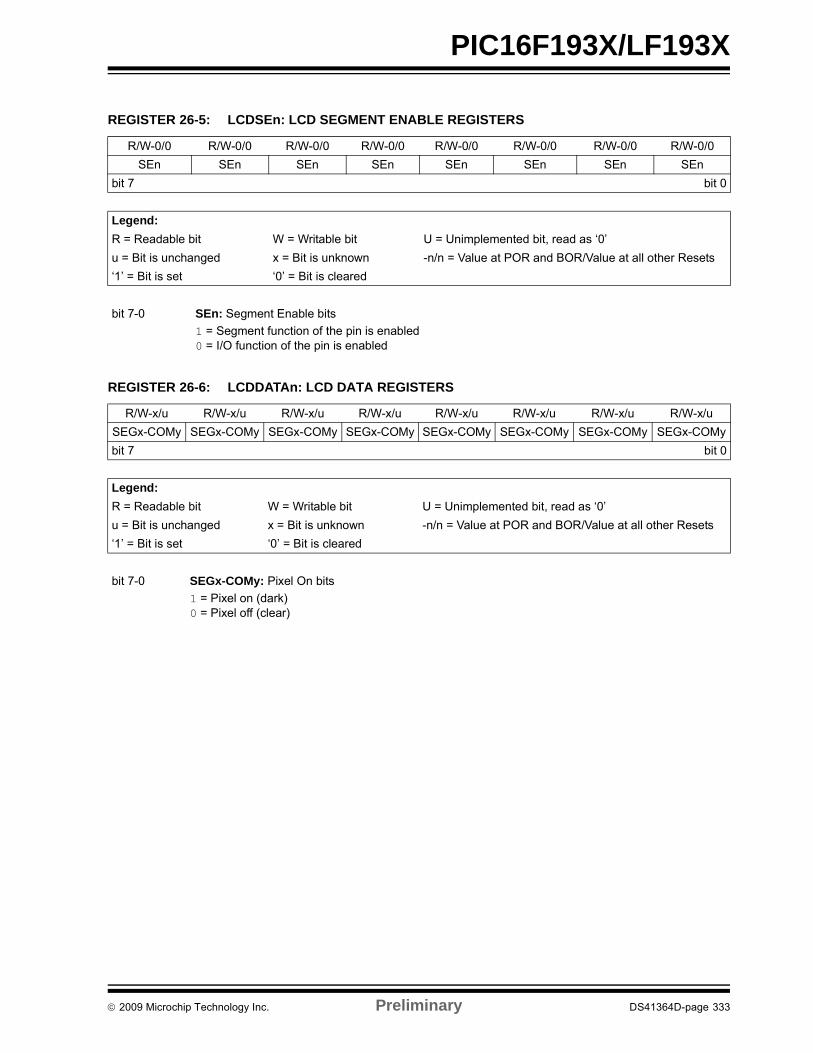
PIC16F193X/LF193X
REGISTER 26-5: LCDSEn: LCD SEGMENT ENABLE REGISTERS
R/W-0/0 R/W-0/0 R/W-0/0 R/W-0/0 R/W-0/0 R/W-0/0 R/W-0/0 R/W-0/0
SEn SEn SEn SEn SEn SEn SEn SEn
bit 7 bit 0
Legend:
R = Readable bit W = Writable bit U = Unimplemented bit, read as ‘0’
u = Bit is unchanged x = Bit is unknown -n/n = Value at POR and BOR/Value at all other Resets
‘1’ = Bit is set ‘0’ = Bit is cleared
bit 7-0 SEn: Segment Enable bits
1 = Segment function of the pin is enabled0 = I/O function of the pin is enabled
REGISTER 26-6: LCDDATAn: LCD DATA REGISTERS
R/W-x/u R/W-x/u R/W-x/u R/W-x/u R/W-x/u R/W-x/u R/W-x/u R/W-x/u
SEGx-COMy SEGx-COMy SEGx-COMy SEGx-COMy SEGx-COMy SEGx-COMy SEGx-COMy SEGx-COMy
bit 7 bit 0
Legend:
R = Readable bit W = Writable bit U = Unimplemented bit, read as ‘0’
u = Bit is unchanged x = Bit is unknown -n/n = Value at POR and BOR/Value at all other Resets
‘1’ = Bit is set ‘0’ = Bit is cleared
bit 7-0 SEGx-COMy: Pixel On bits
1 = Pixel on (dark)0 = Pixel off (clear)
2009 Microchip Technology Inc. Preliminary DS41364D-page 333

PIC16F193X/LF193X
26.2 LCD Clock Source Selection
The LCD module has 3 possible clock sources:
• FOSC/256
• T1OSC
• LFINTOSC
The first clock source is the system clock divided by256 (FOSC/256). This divider ratio is chosen to provideabout 1 kHz output when the system clock is 8 MHz.The divider is not programmable. Instead, the LCDprescaler bits LP<3:0> of the LCDPS register are usedto set the LCD frame clock rate.
The second clock source is the T1OSC. This also givesabout 1 kHz when a 32.768 kHz crystal is used with theTimer1 oscillator. To use the Timer1 oscillator as aclock source, the T1OSCEN bit of the T1CON registershould be set.
The third clock source is the 31 kHz LFINTOSC, whichprovides approximately 1 kHz output.
The second and third clock sources may be used tocontinue running the LCD while the processor is inSleep.
Using bits CS<1:0> of the LCDCON register can selectany of these clock sources.
26.2.1 LCD PRESCALER
A 4-bit counter is available as a prescaler for the LCDclock. The prescaler is not directly readable or writable;its value is set by the LP<3:0> bits of the LCDPS register,which determine the prescaler assignment and prescaleratio.
The prescale values are selectable from 1:1 through1:16.
FIGURE 26-2: LCD CLOCK GENERATION
CS<1:0>
T1OSC 32 kHzCrystal Osc.
LFINTOSCNominal = 31 kHz
Static
1/2
1/3,1/4
÷4
LMUX<1:0>
4-bit Prog ÷1, 2, 3, 4Ring Counter
CO
M0
CO
M1
CO
M2
CO
M3
÷256FOSC
÷2 ÷ 32
LP<3:0>
Prescaler
To Ladder Power Control
Segment
ClockCounter
DS41364D-page 334 Preliminary 2009 Microchip Technology Inc.

PIC16F193X/LF193X
26.3 LCD Bias Voltage Generation
The LCD module can be configured for one of threebias types:
• Static Bias (2 voltage levels: VSS and VLCD)
• 1/2 Bias (3 voltage levels: VSS, 1/2 VLCD and VLCD)
• 1/3 Bias (4 voltage levels: VSS, 1/3 VLCD, 2/3 VLCD and VLCD)
TABLE 26-2: LCD BIAS VOLTAGES
So that the user is not forced to place external compo-nents and use up to three pins for bias voltage generation,internal contrast control and an internal reference ladderare provided internally to the PIC16F193X/LF193X. Bothof these features may be used in conjunction with theexternal VLCD<3:1> pins, to provide maximum flexibility.Refer to Figure 26-3.
FIGURE 26-3: LCD BIAS VOLTAGE GENERATION BLOCK DIAGRAM
Static Bias 1/2 Bias 1/3 Bias
LCD Bias 0 VSS VSS VSS
LCD Bias 1 — 1/2 VDD 1/3 VDD
LCD Bias 2 — 1/2 VDD 2/3 VDD
LCD Bias 3 VLCD3 VLCD3 VLCD3
VDDLCDIRE
x 33.072V
1.024V fromFVR
VLCD3
LCDIRS
LCDIRELCDIRS
LCDCST<2:0>
VLCD3PE
VLCD2
VLCD2PE
VLCD1
VLCD1PE
LCDRLP1
BIASMD
lcdbias3
lcdbias2
lcdbias1
lcdbias0
LCDA
LCDA
LCDA
LCDRLP0
2009 Microchip Technology Inc. Preliminary DS41364D-page 335

PIC16F193X/LF193X
26.4 LCD Bias Internal Reference Ladder
The internal reference ladder can be used to divide theLCD bias voltage two or three equally spaced voltagesthat will be supplied to the LCD segment pins. To createthis, the reference ladder consists of three matchedresistors. Refer to Figure 26-3.
26.4.1 BIAS MODE INTERACTION
When in 1/2 Bias mode (BIASMD = 1), then the middleresistor of the ladder is shorted out so that only twovoltages are generated. The current consumption of theladder is higher in this mode, with the one resistorremoved.
TABLE 26-3: LCD INTERNAL LADDER POWER MODES (1/3 BIAS)
26.4.2 POWER MODES
The internal reference ladder may be operated in one ofthree power modes. This allows the user to trade off LCDcontrast for power in the specific application. The largerthe LCD glass, the more capacitance is present on aphysical LCD segment, requiring more current tomaintain the same contrast level.
Three different power modes are available, LP, MP andHP. The internal reference ladder can also be turned offfor applications that wish to provide an external ladderor to minimize power consumption. Disabling theinternal reference ladder results in all of the laddersbeing disconnected, allowing external voltages to besupplied.
Whenever the LCD module is inactive (LCDA = 0), theinternal reference ladder will be turned off.
Power Mode
Nominal Resistance of Entire Ladder
Nominal IDD
Low 3 Mohm 1 µA
Medium 300 kohm 10 µA
High 30 kohm 100 µA
DS41364D-page 336 Preliminary 2009 Microchip Technology Inc.

PIC16F193X/LF193X
26.4.3 AUTOMATIC POWER MODE SWITCHING
As an LCD segment is electrically only a capacitor, cur-rent is drawn only during the interval where the voltageis switching. To minimize total device current, the LCDinternal reference ladder can be operated in a differentpower mode for the transition portion of the duration.This is controlled by the LCDRL Register(Register 26-7).
The LCDRL register allows switching between twopower modes, designated ‘A’ and ‘B’. ‘A’ Power modeis active for a programmable time, beginning at thetime when the LCD segments transition. ‘B’ Powermode is the remaining time before the segments orcommons change again. The LRLAT<2:0> bits selecthow long, if any, that the ‘A’ Power mode is active.Refer to Figure 26-4.
To implement this, the 5-bit prescaler used to dividethe 32 kHz clock down to the LCD controller’s 1 kHzbase rate is used to select the power mode.
FIGURE 26-4: LCD INTERNAL REFERENCE LADDER POWER MODE SWITCHING DIAGRAM – TYPE A
Single Segment Time
‘H00 ‘H01 ‘H02 ‘H03 ‘H04 ‘H05 ‘H06 ‘H07 ‘H0E ‘H0F ‘H00 ‘H01
‘H3
Power Mode A Power Mode B Mode A
LRLAT<2:0>
32kHz Clock
Ladder Power
Segment Clock
LRLAT<2:0>
Segment Data
Power Mode
COM0
SEG0
COM0-SEG0
Control
V0
V1
V0
V1
V0
V1
-V1
2009 Microchip Technology Inc. Preliminary DS41364D-page 337
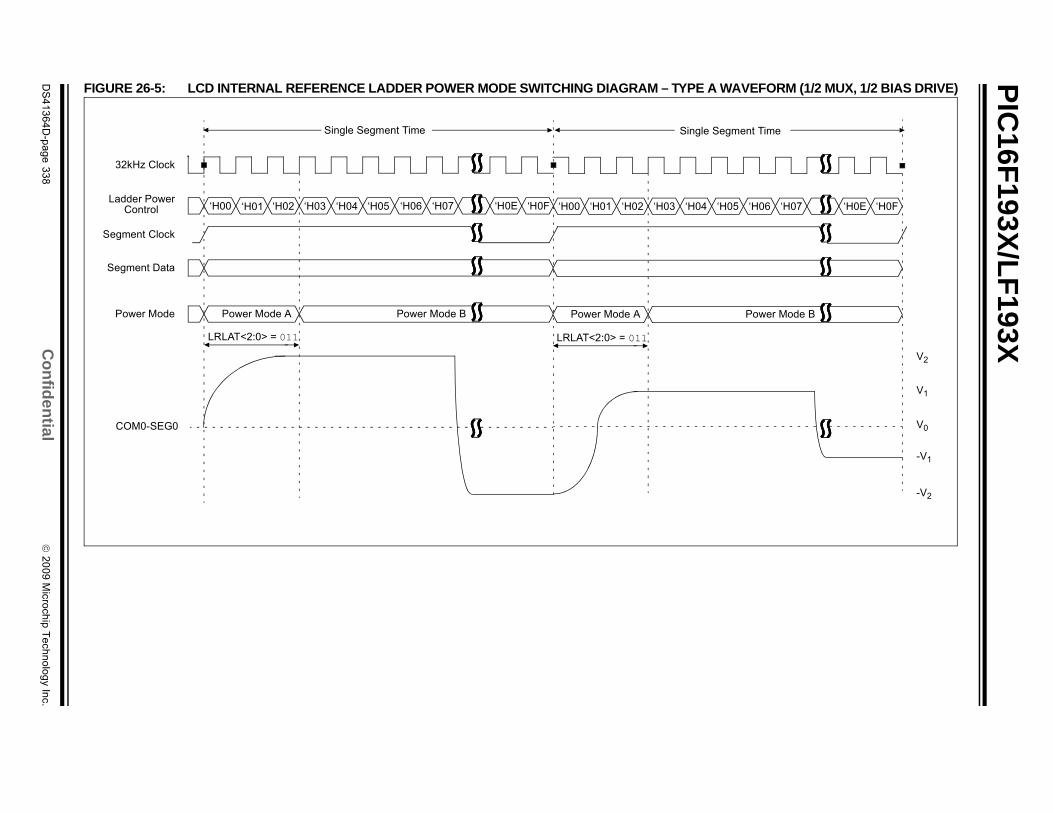
PIC
16F193X
/LF
193X
DS
41
36
4D
-pa
ge
33
8C
on
fiden
tial
2
00
9 M
icroch
ip T
ech
no
log
y Inc.
WAVEFORM (1/2 MUX, 1/2 BIAS DRIVE)
V1
V2
V0
-V2
-V1
egment Time
H05 ‘H06 ‘H07 ‘H0F
Power Mode B
‘H0E
FIGURE 26-5: LCD INTERNAL REFERENCE LADDER POWER MODE SWITCHING DIAGRAM – TYPE A
Single Segment Time
‘H00 ‘H01 ‘H02 ‘H03 ‘H04 ‘H05 ‘H06 ‘H07 ‘H0F
Power Mode A Power Mode B
LRLAT<2:0> = 011
32kHz Clock
Ladder Power
Segment Clock
Segment Data
Power Mode
COM0-SEG0
Control
Single S
‘H00 ‘H01 ‘H02 ‘H03 ‘H04 ‘
Power Mode A
‘H0E
LRLAT<2:0> = 011

2
00
9 M
icroch
ip T
ech
no
log
y Inc.
Co
nfid
entia
lD
S4
13
64
D-p
ag
e 3
39
PIC
16F193X
/LF
193X
FIG EFORM (1/2 MUX, 1/2 BIAS DRIVE)
V1
V2
V0
-V2
-V1
Single Segment Time
‘H11 ‘H12 ‘H13 ‘H1F
er Mode A Power Mode B
‘H1E
T<2:0> = 011
URE 26-6: LCD INTERNAL REFERENCE LADDER POWER MODE SWITCHING DIAGRAM – TYPE B WAV
Single Segment Time
‘H00 ‘H01 ‘H02 ‘H03 ‘H0F
Power Mode A Power Mode B
32kHz Clock
Ladder Power
Segment Clock
Segment Data
Power Mode
COM0-SEG0
Control ‘H0E
Single Segment Time
‘H10 ‘H11 ‘H12 ‘H13 ‘H1F
Power Mode A Power Mode B
‘H1E
Single Segment Time
‘H00 ‘H01 ‘H02 ‘H03 ‘H0F
Power Mode A Power Mode B
‘H0E ‘H10
Pow
LRLAT<2:0> = 011 LRLAT<2:0> = 011 LRLAT<2:0> = 011 LRLA
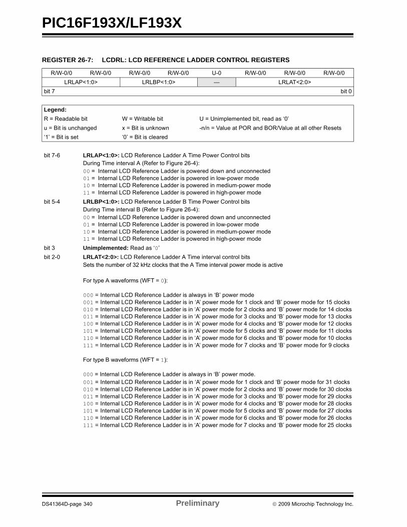
PIC16F193X/LF193X
REGISTER 26-7: LCDRL: LCD REFERENCE LADDER CONTROL REGISTERS
R/W-0/0 R/W-0/0 R/W-0/0 R/W-0/0 U-0 R/W-0/0 R/W-0/0 R/W-0/0
LRLAP<1:0> LRLBP<1:0> — LRLAT<2:0>
bit 7 bit 0
Legend:
R = Readable bit W = Writable bit U = Unimplemented bit, read as ‘0’
u = Bit is unchanged x = Bit is unknown -n/n = Value at POR and BOR/Value at all other Resets
‘1’ = Bit is set ‘0’ = Bit is cleared
bit 7-6 LRLAP<1:0>: LCD Reference Ladder A Time Power Control bitsDuring Time interval A (Refer to Figure 26-4):00 = Internal LCD Reference Ladder is powered down and unconnected01 = Internal LCD Reference Ladder is powered in low-power mode10 = Internal LCD Reference Ladder is powered in medium-power mode 11 = Internal LCD Reference Ladder is powered in high-power mode
bit 5-4 LRLBP<1:0>: LCD Reference Ladder B Time Power Control bitsDuring Time interval B (Refer to Figure 26-4):00 = Internal LCD Reference Ladder is powered down and unconnected01 = Internal LCD Reference Ladder is powered in low-power mode10 = Internal LCD Reference Ladder is powered in medium-power mode11 = Internal LCD Reference Ladder is powered in high-power mode
bit 3 Unimplemented: Read as ‘0’
bit 2-0 LRLAT<2:0>: LCD Reference Ladder A Time interval control bitsSets the number of 32 kHz clocks that the A Time interval power mode is active
For type A waveforms (WFT = 0):
000 = Internal LCD Reference Ladder is always in ‘B’ power mode001 = Internal LCD Reference Ladder is in ‘A’ power mode for 1 clock and ‘B’ power mode for 15 clocks010 = Internal LCD Reference Ladder is in ‘A’ power mode for 2 clocks and ‘B’ power mode for 14 clocks011 = Internal LCD Reference Ladder is in ‘A’ power mode for 3 clocks and ‘B’ power mode for 13 clocks100 = Internal LCD Reference Ladder is in ‘A’ power mode for 4 clocks and ‘B’ power mode for 12 clocks101 = Internal LCD Reference Ladder is in ‘A’ power mode for 5 clocks and ‘B’ power mode for 11 clocks110 = Internal LCD Reference Ladder is in ‘A’ power mode for 6 clocks and ‘B’ power mode for 10 clocks111 = Internal LCD Reference Ladder is in ‘A’ power mode for 7 clocks and ‘B’ power mode for 9 clocks
For type B waveforms (WFT = 1):
000 = Internal LCD Reference Ladder is always in ‘B’ power mode.001 = Internal LCD Reference Ladder is in ‘A’ power mode for 1 clock and ‘B’ power mode for 31 clocks010 = Internal LCD Reference Ladder is in ‘A’ power mode for 2 clocks and ‘B’ power mode for 30 clocks011 = Internal LCD Reference Ladder is in ‘A’ power mode for 3 clocks and ‘B’ power mode for 29 clocks100 = Internal LCD Reference Ladder is in ‘A’ power mode for 4 clocks and ‘B’ power mode for 28 clocks101 = Internal LCD Reference Ladder is in ‘A’ power mode for 5 clocks and ‘B’ power mode for 27 clocks110 = Internal LCD Reference Ladder is in ‘A’ power mode for 6 clocks and ‘B’ power mode for 26 clocks111 = Internal LCD Reference Ladder is in ‘A’ power mode for 7 clocks and ‘B’ power mode for 25 clocks
DS41364D-page 340 Preliminary 2009 Microchip Technology Inc.

PIC16F193X/LF193X
26.4.4 CONTRAST CONTROL
The LCD contrast control circuit consists of aseven-tap resistor ladder, controlled by the LCDCSTbits. Refer to Figure 26-7.
The contrast control circuit is used to decrease theoutput voltage of the signal source by a total ofapproximately 10%, when LCDCST = 111.
Whenever the LCD module is inactive (LCDA = 0), thecontrast control ladder will be turned off (open).
FIGURE 26-7: INTERNAL REFERENCE AND CONTRAST CONTROL BLOCK DIAGRAM
26.4.5 INTERNAL REFERENCE
Under firmware control, an internal reference for theLCD bias voltages can be enabled. When enabled, thesource of this voltage can be either VDDIO or a voltage3 times the main fixed voltage reference (3.072V).When no internal reference is selected, the LCD con-trast control circuit is disabled and LCD bias must beprovided externally.
Whenever the LCD module is inactive (LCDA = 0), theinternal reference will be turned off.
When the internal reference is enabled and the FixedVoltage Reference is selected, the LCDIRI bit can beused to minimize power consumption by tieing into theLCD reference ladder automatic power mode switch-ing. When LCDIRI = 1 and the LCD reference ladder isin power mode ‘B’, the LCD internal FVR buffer isdisabled.
.
26.4.6 VLCD<3:1> PINS
The VLCD<3:1> pins provide the ability for an externalLCD bias network to be used instead of the internal lad-der. Use of the VLCD<3:1> pins does not prevent useof the internal ladder. Each VLCD pin has an indepen-dent control in the LCDREF register (Register 26-3),allowing access to any or all of the LCD Bias signals.This architecture allows for maximum flexibility in differ-ent applications
For example, the VLCD<3:1> pins may be used to addcapacitors to the internal reference ladder, increasingthe drive capacity.
For applications where the internal contrast control isinsufficient, the firmware can choose to only enable theVLCD3 pin, allowing an external contrast control circuitto use the internal reference divider.
LCDCST<2:0>
Analog
R R R R
7 Stages
MUX
To top of Reference Ladder
7
0
3
3.072V
VDDIO
From FVRBuffer
Internal Reference Contrast control
Note: The LCD module automatically turns on thefixed voltage reference when needed.
2009 Microchip Technology Inc. Preliminary DS41364D-page 341

PIC16F193X/LF193X
26.5 LCD Multiplex Types
The LCD driver module can be configured into one offour multiplex types:
• Static (only COM0 is used)
• 1/2 multiplex (COM<1:0> are used)
• 1/3 multiplex (COM<2:0> are used)
• 1/4 multiplex (COM<3:0> are used)
The LMUX<1:0> bit setting of the LCDCON registerdecides which of the LCD common pins are used (seeTable 26-4 for details).
If the pin is a digital I/O, the corresponding TRIS bitcontrols the data direction. If the pin is a COM drive,then the TRIS setting of that pin is overridden.
TABLE 26-4: COMMON PIN USAGE
26.6 Segment Enables
The LCDSEn registers are used to select the pinfunction for each segment pin. The selection allowseach pin to operate as either an LCD segment driver oras one of the pin’s alternate functions. To configure thepin as a segment pin, the corresponding bits in theLCDSEn registers must be set to ‘1’.
If the pin is a digital I/O, the corresponding TRIS bitcontrols the data direction. Any bit set in the LCDSEnregisters overrides any bit settings in the correspondingTRIS register.
26.7 Pixel Control
The LCDDATAx registers contain bits which define thestate of each pixel. Each bit defines one unique pixel.
Register 26-6 shows the correlation of each bit in theLCDDATAx registers to the respective common andsegment signals.
Any LCD pixel location not being used for display canbe used as general purpose RAM.
26.8 LCD Frame Frequency
The rate at which the COM and SEG outputs change iscalled the LCD frame frequency.
TABLE 26-5: FRAME FREQUENCY FORMULAS
TABLE 26-6: APPROXIMATE FRAME FREQUENCY (IN Hz) USING FOSC @ 8 MHz, TIMER1 @ 32.768 kHz OR LFINTOSC
MultiplexLMUX<1:0>
COM3 COM2 COM1
Static 00 Unused Unused Unused
1/2 01 Unused Unused Active
1/3 10 Unused Active Active
1/4 11 Active Active Active
Note: On a Power-on Reset, these pins areconfigured as normal I/O, not LCD pins.
Multiplex Frame Frequency =
Static Clock source/(4 x 1 x (LP<3:0> + 1))
1/2 Clock source/(2 x 2 x (LP<3:0> + 1))
1/3 Clock source/(1 x 3 x (LP<3:0> + 1))
1/4 Clock source/(1 x 4 x (LP<3:0> + 1))
Note: Clock source is FOSC/256, T1OSC orLFINTOSC.
LP<3:0> Static 1/2 1/3 1/4
2 85 85 114 85
3 64 64 85 64
4 51 51 68 51
5 43 43 57 43
6 37 37 49 37
7 32 32 43 32
DS41364D-page 342 Preliminary 2009 Microchip Technology Inc.

PIC16F193X/LF193X
TABLE 26-7: LCD SEGMENT MAPPING WORKSHEET
LCDFunction
COM0 COM1 COM2 COM3
LCDDATAxAddress
LCDSegment
LCDDATAxAddress
LCDSegment
LCDDATAxAddress
LCDSegment
LCDDATAxAddress
LCDSegment
SEG0 LCDDATA0, 0 LCDDATA3, 0 LCDDATA6, 0 LCDDATA9, 0
SEG1 LCDDATA0, 1 LCDDATA3, 1 LCDDATA6, 1 LCDDATA9, 1
SEG2 LCDDATA0, 2 LCDDATA3, 2 LCDDATA6, 2 LCDDATA9, 2
SEG3 LCDDATA0, 3 LCDDATA3, 3 LCDDATA6, 3 LCDDATA9, 3
SEG4 LCDDATA0, 4 LCDDATA3, 4 LCDDATA6, 4 LCDDATA9, 4
SEG5 LCDDATA0, 5 LCDDATA3, 5 LCDDATA6, 5 LCDDATA9, 5
SEG6 LCDDATA0, 6 LCDDATA3, 6 LCDDATA6, 6 LCDDATA9, 6
SEG7 LCDDATA0, 7 LCDDATA3, 7 LCDDATA6, 7 LCDDATA9, 7
SEG8 LCDDATA1, 0 LCDDATA4, 0 LCDDATA7, 0 LCDDATA10, 0
SEG9 LCDDATA1, 1 LCDDATA4, 1 LCDDATA7, 1 LCDDATA10, 1
SEG10 LCDDATA1, 2 LCDDATA4, 2 LCDDATA7, 2 LCDDATA10, 2
SEG11 LCDDATA1, 3 LCDDATA4, 3 LCDDATA7, 3 LCDDATA10, 3
SEG12 LCDDATA1, 4 LCDDATA4, 4 LCDDATA7, 4 LCDDATA10, 4
SEG13 LCDDATA1, 5 LCDDATA4, 5 LCDDATA7, 5 LCDDATA10, 5
SEG14 LCDDATA1, 6 LCDDATA4, 6 LCDDATA7, 6 LCDDATA10, 6
SEG15 LCDDATA1, 7 LCDDATA4, 7 LCDDATA7, 7 LCDDATA10, 7
SEG16 LCDDATA2, 0 LCDDATA5, 0 LCDDATA8, 0 LCDDATA11, 0
SEG17 LCDDATA2, 1 LCDDATA5, 1 LCDDATA8, 1 LCDDATA11, 1
SEG18 LCDDATA2, 2 LCDDATA5, 2 LCDDATA8, 2 LCDDATA11, 2
SEG19 LCDDATA2, 3 LCDDATA5, 3 LCDDATA8, 3 LCDDATA11, 3
SEG20 LCDDATA2, 4 LCDDATA5, 4 LCDDATA8, 4 LCDDATA11, 4
SEG21 LCDDATA2, 5 LCDDATA5, 5 LCDDATA8, 5 LCDDATA11, 5
SEG22 LCDDATA2, 6 LCDDATA5, 6 LCDDATA8, 6 LCDDATA11, 6
SEG23 LCDDATA2, 7 LCDDATA5, 7 LCDDATA8, 7 LCDDATA11, 7
2009 Microchip Technology Inc. Preliminary DS41364D-page 343

PIC16F193X/LF193X
26.9 LCD Waveform Generation
LCD waveforms are generated so that the net ACvoltage across the dark pixel should be maximized andthe net AC voltage across the clear pixel should beminimized. The net DC voltage across any pixel shouldbe zero.
The COM signal represents the time slice for eachcommon, while the SEG contains the pixel data.
The pixel signal (COM-SEG) will have no DCcomponent and it can take only one of the two RMSvalues. The higher RMS value will create a dark pixeland a lower RMS value will create a clear pixel.
As the number of commons increases, the deltabetween the two RMS values decreases. The deltarepresents the maximum contrast that the display canhave.
The LCDs can be driven by two types of waveform:Type-A and Type-B. In Type-A waveform, the phasechanges within each common type, whereas in Type-Bwaveform, the phase changes on each frameboundary. Thus, Type-A waveform maintains 0 VDC
over a single frame, whereas Type-B waveform takestwo frames.
Figure 26-8 through Figure 26-18 provide waveformsfor static, half-multiplex, 1/3-multiplex and 1/4-multiplexdrives for Type-A and Type-B waveforms.
FIGURE 26-8: TYPE-A/TYPE-B WAVEFORMS IN STATIC DRIVE
Note 1: If Sleep has to be executed with LCDSleep disabled (LCDCON<SLPEN> is‘1’), then care must be taken to executeSleep only when VDC on all the pixels is‘0’.
2: When the LCD clock source is FOSC/256,if Sleep is executed, irrespective of theLCDCON<SLPEN> setting, the LCDimmediately goes into Sleep. Thus, takecare to see that VDC on all pixels is ‘0’when Sleep is executed.
V1
V0COM0 pin
SEG0 pin
COM0-SEG0
COM0-SEG1
SEG1 pin
V1
V0
V1
V0
V0
V1
-V1
V0
1 Frame
COM0
SE
G0
SE
G1
SE
G2
SE
G3
SE
G4
SE
G5
SE
G6
SE
G7
segment voltage(active)
segment voltage(inactive)
DS41364D-page 344 Preliminary 2009 Microchip Technology Inc.

PIC16F193X/LF193X
FIGURE 26-9: TYPE-A WAVEFORMS IN 1/2 MUX, 1/2 BIAS DRIVE
V2
V1
V0
V2
V1
V0
V2
V1
V0
V2
V1
V0
V2
V1
V0
-V2
-V1
V2
V1
V0
-V2
-V1
COM0 pin
COM1 pin
SEG0 pin
SEG1 pin
COM0-SEG0
COM0-SEG1
1 Frame
COM1
COM0
SE
G0
SE
G1
SE
G2
SE
G3
1 Segment Time
Note: 1 Frame = 2 single segment times.
segment voltage
segment voltage
(active)
(inactive)
2009 Microchip Technology Inc. Preliminary DS41364D-page 345

PIC16F193X/LF193X
FIGURE 26-10: TYPE-B WAVEFORMS IN 1/2 MUX, 1/2 BIAS DRIVE
V2
V1
V0
V2
V1
V0
V2
V1
V0
V2
V1
V0
V2
V1
V0
-V2
-V1
V2
V1
V0
-V2
-V1
COM0 pin
COM1 pin
SEG0 pin
SEG1 pin
COM0-SEG0
COM0-SEG1
COM1
COM0
SE
G2
SE
G3
2 Frames
Note: 1 Frame = 2 single segment times.
1 Segment Time
segment voltage(active)
segment voltage(inactive)
SE
G0
SE
G1
DS41364D-page 346 Preliminary 2009 Microchip Technology Inc.
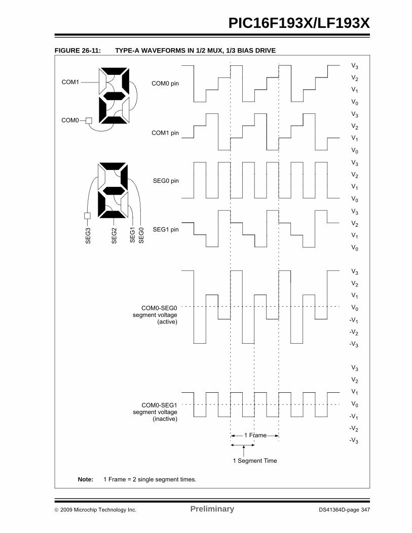
PIC16F193X/LF193X
FIGURE 26-11: TYPE-A WAVEFORMS IN 1/2 MUX, 1/3 BIAS DRIVE
V3
V2
V1
V0
V3
V2
V1
V0
V3
V2
V1
V0
V3
V2
V1
V0
V3
V2
V1
V0
-V3
-V2
-V1
V3
V2
V1
V0
-V3
-V2
-V1
COM0 pin
COM1 pin
SEG0 pin
SEG1 pin
COM0-SEG0
COM0-SEG1
1 Frame
COM1
COM0S
EG
2
SE
G3
segment voltage(active)
segment voltage(inactive)
SE
G0
SE
G1
1 Segment Time
Note: 1 Frame = 2 single segment times.
2009 Microchip Technology Inc. Preliminary DS41364D-page 347

PIC16F193X/LF193X
FIGURE 26-12: TYPE-B WAVEFORMS IN 1/2 MUX, 1/3 BIAS DRIVE
V3
V2
V1
V0
V3
V2
V1
V0
V3
V2
V1
V0
V3
V2
V1
V0
V3
V2
V1
V0
-V3
-V2
-V1
V3
V2
V1
V0
-V3
-V2
-V1
COM0 pin
COM1 pin
SEG0 pin
SEG1 pin
COM0-SEG0
COM0-SEG1
COM1
COM0
SE
G2
SE
G3
segment voltage(active)
segment voltage(inactive)
SE
G0
SE
G1
2 Frames
Note: 1 Frame = 2 single segment times.
1 Segment Time
DS41364D-page 348 Preliminary 2009 Microchip Technology Inc.

PIC16F193X/LF193X
FIGURE 26-13: TYPE-A WAVEFORMS IN 1/3 MUX, 1/2 BIAS DRIVE
V2
V1
V0
V2
V1
V0
V2
V1
V0
V2
V1
V0
V2
V1
V0
V2
V1
V0
-V2
-V1
V2
V1
V0
-V2
-V1
COM0 pin
COM1 pin
COM2 pin
SEG0 and
SEG1 pin
COM0-SEG0
COM0-SEG1
COM2
COM1
COM0S
EG
0
SE
G1
SE
G2
SEG2 pins
segment voltage(inactive)
segment voltage(active)
1 Frame
1 Segment Time
Note: 1 Frame = 2 single segment times.
2009 Microchip Technology Inc. Preliminary DS41364D-page 349

PIC16F193X/LF193X
FIGURE 26-14: TYPE-B WAVEFORMS IN 1/3 MUX, 1/2 BIAS DRIVE
V2
V1
V0
V2
V1
V0
V2
V1
V0
V2
V1
V0
V2
V1
V0
V2
V1
V0
-V2
-V1
V2
V1
V0
-V2
-V1
COM0 pin
COM1 pin
COM2 pin
SEG0 pin
SEG1 pin
COM0-SEG0
COM0-SEG1
COM2
COM1
COM0
SE
G0
SE
G1
SE
G2
segment voltage(inactive)
segment voltage(active)
2 Frames
Note: 1 Frame = 2 single segment times.
1 Segment Time
DS41364D-page 350 Preliminary 2009 Microchip Technology Inc.

PIC16F193X/LF193X
FIGURE 26-15: TYPE-A WAVEFORMS IN 1/3 MUX, 1/3 BIAS DRIVE
V3
V2
V1
V0
V3
V2
V1
V0
V3
V2
V1
V0
V3
V2
V1
V0
V3
V2
V1
V0
V3
V2
V1
V0
-V3
-V2
-V1
V3
V2
V1
V0
-V3
-V2
-V1
COM0 pin
COM1 pin
COM2 pin
SEG0 and
SEG1 pin
COM0-SEG0
COM0-SEG1
COM2
COM1
COM0S
EG
0
SE
G1
SE
G2
SEG2 pins
segment voltage(inactive)
segment voltage(active)
1 Frame
1 Segment Time
Note: 1 Frame = 2 single segment times.
2009 Microchip Technology Inc. Preliminary DS41364D-page 351

PIC16F193X/LF193X
FIGURE 26-16: TYPE-B WAVEFORMS IN 1/3 MUX, 1/3 BIAS DRIVE
V3
V2
V1
V0
V3
V2
V1
V0
V3
V2
V1
V0
V3
V2
V1
V0
V3
V2
V1
V0
V3
V2
V1
V0
-V3
-V2
-V1
V3
V2
V1
V0
-V3
-V2
-V1
COM0 pin
COM1 pin
COM2 pin
SEG0 pin
SEG1 pin
COM0-SEG0
COM0-SEG1
COM2
COM1
COM0
SE
G0
SE
G1
SE
G2
segment voltage(inactive)
segment voltage(active)
2 Frames
Note: 1 Frame = 2 single segment times.
1 Segment Time
DS41364D-page 352 Preliminary 2009 Microchip Technology Inc.

PIC16F193X/LF193X
FIGURE 26-17: TYPE-A WAVEFORMS IN 1/4 MUX, 1/3 BIAS DRIVE
V3V2V1V0
V3V2V1V0
V3V2V1V0
V3V2V1V0
V3V2V1V0
V3V2V1V0
V3V2V1V0
-V3
-V2
-V1
V3V2V1V0
-V3
-V2
-V1
COM0 pin
COM1 pin
COM2 pin
COM3 pin
SEG0 pin
SEG1 pin
COM0-SEG0
COM0-SEG1
COM3
COM2
COM1
COM0
SE
G0
SE
G1
segment voltage(active)
segment voltage(inactive)
1 Frame
1 Segment Time
Note: 1 Frame = 2 single segment times.
2009 Microchip Technology Inc. Preliminary DS41364D-page 353

PIC16F193X/LF193X
FIGURE 26-18: TYPE-B WAVEFORMS IN 1/4 MUX, 1/3 BIAS DRIVE
V3V2V1V0
V3V2V1V0
V3V2V1V0
V3V2V1V0
V3V2V1V0
V3V2V1V0
V3V2V1V0
-V3
-V2
-V1
V3V2V1V0
-V3
-V2
-V1
COM0 pin
COM1 pin
COM2 pin
COM3 pin
SEG0 pin
SEG1 pin
COM0-SEG0
COM0-SEG1
COM2
COM1
COM0
SE
G0
SE
G1
COM3
segment voltage(active)
segment voltage(inactive)
2 Frames
Note: 1 Frame = 2 single segment times.
1 Segment Time
DS41364D-page 354 Preliminary 2009 Microchip Technology Inc.

PIC16F193X/LF193X
26.10 LCD Interrupts
The LCD module provides an interrupt in two cases. Aninterrupt when the LCD controller goes from active toinactive controller. An interrupt also provides unframeboundaries for Type B waveform. The LCD timing gen-eration provides an interrupt that defines the LCDframe timing.
26.10.1 LCD INTERRUPT ON MODULE SHUTDOWN
An LCD interrupt is generated when the module com-pletes shutting down (LCDA goes from ‘1’ to ‘0’).
26.10.2 LCD FRAME INTERRUPTS
A new frame is defined to begin at the leading edge ofthe COM0 common signal. The interrupt will be setimmediately after the LCD controller completes access-ing all pixel data required for a frame. This will occur ata fixed interval before the frame boundary (TFINT), asshown in Figure 26-19. The LCD controller will begin toaccess data for the next frame within the interval fromthe interrupt to when the controller begins to accessdata after the interrupt (TFWR). New data must be writ-ten within TFWR, as this is when the LCD controller willbegin to access the data for the next frame.
When the LCD driver is running with Type-B waveformsand the LMUX<1:0> bits are not equal to ‘00’ (staticdrive), there are some additional issues that must beaddressed. Since the DC voltage on the pixel takes twoframes to maintain zero volts, the pixel data must notchange between subsequent frames. If the pixel datawere allowed to change, the waveform for the oddframes would not necessarily be the complement of thewaveform generated in the even frames and a DCcomponent would be introduced into the panel.Therefore, when using Type-B waveforms, the usermust synchronize the LCD pixel updates to occur withina subframe after the frame interrupt.
To correctly sequence writing while in Type-B, theinterrupt will only occur on complete phase intervals. Ifthe user attempts to write when the write is disabled,the WERR bit of the LCDCON register is set and thewrite does not occur.
Note: The LCD frame interrupt is not generatedwhen the Type-A waveform is selected andwhen the Type-B with no multiplex (static)is selected.
2009 Microchip Technology Inc. Preliminary DS41364D-page 355
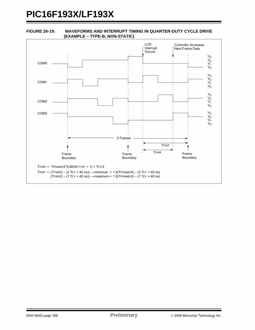
PIC16F193X/LF193X
FIGURE 26-19: WAVEFORMS AND INTERRUPT TIMING IN QUARTER-DUTY CYCLE DRIVE (EXAMPLE – TYPE-B, NON-STATIC)
FrameBoundary
FrameBoundary
LCDInterruptOccurs
Controller AccessesNext Frame Data
TFINT
TFWR
TFWR = TFRAME/2*(LMUX<1:0> + 1) + TCY/2
TFINT = (TFWR/2 – (2 TCY + 40 ns)) minimum = 1.5(TFRAME/4) – (2 TCY + 40 ns)(TFWR/2 – (1 TCY + 40 ns)) maximum = 1.5(TFRAME/4) – (1 TCY + 40 ns)
FrameBoundary
V3V2V1V0
V3V2V1V0
V3V2V1V0
V3V2V1V0
COM0
COM1
COM2
COM3
2 Frames
DS41364D-page 356 Preliminary 2009 Microchip Technology Inc.
PIC16F193X/LF193X
26.11 Operation During Sleep
The LCD module can operate during Sleep. Theselection is controlled by bit SLPEN of the LCDCONregister. Setting the SLPEN bit allows the LCD moduleto go to Sleep. Clearing the SLPEN bit allows themodule to continue to operate during Sleep.
If a SLEEP instruction is executed and SLPEN = 1, theLCD module will cease all functions and go into a verylow-current Consumption mode. The module will stopoperation immediately and drive the minimum LCDvoltage on both segment and common lines.Figure 26-20 shows this operation.
The LCD module can be configured to operate duringSleep. The selection is controlled by bit SLPEN of theLCDCON register. Clearing SLPEN and correctly con-figuring the LCD module clock will allow the LCD mod-ule to operate during Sleep. Setting SLPEN andcorrectly executing the LCD module shutdown will dis-able the LCD module during Sleep and save power.
If a SLEEP instruction is executed and SLPEN = 1, theLCD module will immediately cease all functions, drivethe outputs to Vss and go into a very low-current mode.The SLEEP instruction should only be executed afterthe LCD module has been disabled and the currentcycle completed, thus ensuring that there are no DCvoltages on the glass. To disable the LCD module,clear the LCDEN bit. The LCD module will complete thedisabling process after the current frame, clear theLCDA bit and optionally cause an interrupt.
The steps required to properly enter Sleep with theLCD disabled are:
• Clear LCDEN
• Wait for LCDA = 0 either by polling or by interrupt
• Execute SLEEP
If SLPEN = 0 and SLEEP is executed while the LCDmodule clock source is FOSC/4, then the LCD modulewill halt with the pin driving the last LCD voltage pat-tern. Prolonged exposure to a fixed LCD voltage pat-tern will cause damage to the LCD glass. To preventLCD glass damage, either perform the proper LCDmodule shutdown prior to Sleep, or change the LCDmodule clock to allow the LCD module to continueoperation during Sleep.
If a SLEEP instruction is executed and SLPEN = 0 andthe LCD module clock is either T1OSC or LFINTOSC,the module will continue to display the current contentsof the LCDDATA registers. While in Sleep, the LCDdata cannot be changed. If the LCDIE bit is set, thedevice will wake from Sleep on the next LCD frameboundary. The LCD module current consumption willnot decrease in this mode; however, the overall devicepower consumption will be lower due to the shutdownof the CPU and other peripherals.
Table 26-8 shows the status of the LCD module duringa Sleep while using each of the three available clocksources.
If a SLEEP instruction is executed and SLPEN = 0, themodule will continue to display the current contents ofthe LCDDATA registers. To allow the module tocontinue operation while in Sleep, the clock sourcemust be either the LFINTOSC or T1OSC externaloscillator. While in Sleep, the LCD data cannot bechanged. The LCD module current consumption willnot decrease in this mode; however, the overallconsumption of the device will be lower due to shutdown of the core and other peripheral functions.
Table 26-8 shows the status of the LCD module duringSleep while using each of the three available clocksources:
TABLE 26-8: LCD MODULE STATUS DURING SLEEP
If LCD interrupts are being generated (Type-B wave-form with a multiplex mode not static) and LCDIE = 1,the device will awaken from Sleep on the next frameboundary.
Note: When the LCDEN bit is cleared, the LCDmodule will be disabled at the completionof frame. At this time, the port pins willrevert to digital functionality. To minimizepower consumption due to floating digitalinputs, the LCD pins should be driven lowusing the PORT and TRIS registers.
Clock Source SLPENOperational
During Sleep
T1OSC0 Yes
1 No
LFINTOSC0 Yes
1 No
FOSC/40 No
1 No
Note: The LFINTOSC or external T1OSCoscillator must be used to operate the LCDmodule during Sleep.
2009 Microchip Technology Inc. Preliminary DS41364D-page 357

PIC16F193X/LF193X
FIGURE 26-20: SLEEP ENTRY/EXIT WHEN SLPEN = 1
SLEEP Instruction Execution Wake-up
2 Frames
V3
V2
V1
V0
V3
V2
V1
V0
V3
V2
V1
V0
V3
V2
V1
V0
COM0
COM1
COM2
SEG0
DS41364D-page 358 Preliminary 2009 Microchip Technology Inc.
PIC16F193X/LF193X
26.12 Configuring the LCD Module
The following is the sequence of steps to configure theLCD module.
1. Select the frame clock prescale using bitsLP<3:0> of the LCDPS register.
2. Configure the appropriate pins to function assegment drivers using the LCDSEn registers.
3. Configure the LCD module for the followingusing the LCDCON register:
- Multiplex and Bias mode, bits LMUX<1:0>
- Timing source, bits CS<1:0>
- Sleep mode, bit SLPEN
4. Write initial values to pixel data registers,LCDDATA0 through LCDDATA11 (LCDDATA23on PIC16F1938).
5. Clear LCD Interrupt Flag, LCDIF bit of the PIR2register and if desired, enable the interrupt bysetting bit LCDIE of the PIE2 register.
6. Configure bias voltages by setting the LCDRL, LCDREF and the associated ANSELx registers as needed.
7. Enable the LCD module by setting bit LCDEN ofthe LCDCON register.
26.13 Disabling the LCD Module
To disable the LCD module, write all ‘0’s to theLCDCON register.
26.14 LCD Current Consumption
When using the LCD module the current consumptionconsists of the following three factors:
• Oscillator Selection
• LCD Bias Source
• Capacitance of the LCD segments
The current consumption of just the LCD module canbe considered negligible compared to these otherfactors.
26.14.1 OSCILLATOR SELECTION
The current consumed by the clock source selectedmust be considered when using the LCD module. SeeSection 29.0 “Electrical Specifications” for oscillatorcurrent consumption information.
26.14.2 LCD BIAS SOURCE
The LCD bias source, internal or external, can contrib-ute significantly to the current consumption. Use thehighest possible resistor values while maintainingcontrast to minimize current.
26.14.3 CAPACITANCE OF THE LCD SEGMENTS
The LCD segments which can be modeled as capaci-tors which must be both charged and discharged everyframe. The size of the LCD segment and its technologydetermines the segment’s capacitance.
2009 Microchip Technology Inc. Preliminary DS41364D-page 359

PIC16F193X/LF193X
TABLE 26-9: SUMMARY OF REGISTERS ASSOCIATED WITH LCD OPERATION
Name Bit 7 Bit 6 Bit 5 Bit 4 Bit 3 Bit 2 Bit 1 Bit 0Register on Page
INTCON GIE PEIE TMR0IE INTE IOCIE TMR0IF INTF IOCIF 99
LCDCON LCDEN SLPEN WERR — CS<1:0> LMUX<1:0> 329
LCDCST — — — — — LCDCST<2:0> 332
LCDDATA0 SEG7COM0
SEG6COM0
SEG5COM0
SEG4COM0
SEG3COM0
SEG2COM0
SEG1COM0
SEG0COM0
333
LCDDATA1 SEG15COM0
SEG14COM0
SEG13COM0
SEG12COM0
SEG11COM0
SEG10COM0
SEG9COM0
SEG8COM0
333
LCDDATA2 SEG23COM0
SEG22COM0
SEG21COM0
SEG20COM0
SEG19COM0
SEG18COM0
SEG17COM0
SEG16COM0
333
LCDDATA3 SEG7COM1
SEG6COM1
SEG5COM1
SEG4COM1
SEG3COM1
SEG2COM1
SEG1COM1
SEG0COM1
333
LCDDATA4 SEG15COM1
SEG14COM1
SEG13COM1
SEG12COM1
SEG11COM1
SEG10COM1
SEG9COM1
SEG8COM1
333
LCDDATA5 SEG23COM1
SEG22COM1
SEG21COM1
SEG20COM1
SEG19COM1
SEG18COM1
SEG17COM1
SEG16COM1
333
LCDDATA6 SEG7COM2
SEG6COM2
SEG5COM2
SEG4COM2
SEG3COM2
SEG2COM2
SEG1COM2
SEG0COM2
333
LCDDATA7 SEG15COM2
SEG14COM2
SEG13COM2
SEG12COM2
SEG11COM2
SEG10COM2
SEG9COM2
SEG8COM2
333
LCDDATA8 SEG23COM2
SEG22COM2
SEG21COM2
SEG20COM2
SEG19COM2
SEG18COM2
SEG17COM2
SEG16COM2
333
LCDDATA9 SEG7COM3
SEG6COM3
SEG5COM3
SEG4COM3
SEG3COM3
SEG2COM3
SEG1COM3
SEG0COM3
333
LCDDATA10 SEG15COM3
SEG14COM3
SEG13COM3
SEG12COM3
SEG11COM3
SEG10COM3
SEG9COM3
SEG8COM3
333
LCDDATA11 SEG23COM3
SEG22COM3
SEG21COM3
SEG20COM3
SEG19COM3
SEG18COM3
SEG17COM3
SEG16COM3
333
LCDPS WFT BIASMD LCDA WA LP<3:0> 330
LCDREF LCDIRE LCDIRS LCDIRI — VLCD3PE VLCD2PE VLCD1PE — 331
LCDRL LRLAP<1:0> LRLBP<1:0> — LRLAT<2:0> 340
LCDSE0 SE<7:0> 333
LCDSE1 SE<15:8> 333
LCDSE2 SE<23:16> 333
PIE2 OSFIE C2IE C1IE EEIE BCLIE LCDIE — CCP2IE 101
PIR2 OSFIF C2IF C1IF EEIF BCLIF LCDIF — CCP2IF 104
T1CON TMR1CS<1:0> T1CKPS<1:0> T1OSCEN T1SYNC — TMR1ON 201
Legend: — = unimplemented location, read as ‘0’. Shaded cells are not used by the LCD module.
DS41364D-page 360 Preliminary 2009 Microchip Technology Inc.

PIC16F193X/LF193X
27.0 IN-CIRCUIT SERIAL PROGRAMMING™ (ICSP™)
ICSP™ programming allows customers to manufacturecircuit boards with unprogrammed devices. Programmingcan be done after the assembly process allowing thedevice to be programmed with the most recent firmwareor a custom firmware. Five pins are needed for ICSP™programming:
• ICSPCLK
• ICSPDAT
• MCLR/VPP
• VDD
• VSS
In Program/Verify mode the Program Memory, User IDsand the Configuration Words are programmed throughserial communications. The ICSPDAT pin is a bidirec-tional I/O used for transferring the serial data and theICSPCLK pin is the clock input. For more information onICSP™ refer to the “PIC16193X/PIC16LF193X MemoryProgramming Specification” (DS41360A).
27.1 High-Voltage Programming Entry Mode
The device is placed into High-Voltage ProgrammingEntry mode by holding the ICSPCLK and ICSPDATpins low then raising the voltage on MCLR/VPP to VIHH.
Some programmers produce VPP greater than VIHH
(9.0V), an external circuit is required to limit the VPP
voltage. See Figure 27-1 for example circuit.
FIGURE 27-1: VPP LIMITER EXAMPLE CIRCUIT
VREF
VPP
VDD
VSS
ICSP_DATAICSP_CLOCK
NC
RJ11-6PIN
RJ11-6PIN
R1
270 Ohm
To MPLAB® ICD 2 To Target Board
123456 1
23456
R2 R3
10k 1% 24k 1%
U1
LM431BCMX
A2367
8
AAA
K
NCNC
1
45
Note: The ICD 2 produces a VPP voltage greaterthan the maximum VPP specification of thePIC16F193X/LF193X.
2009 Microchip Technology Inc. Preliminary DS41364D-page 361

PIC16F193X/LF193X
27.2 Low-Voltage Programming Entry Mode
The Low-Voltage Programming Entry mode allows thePIC16F193X/LF193X devices to be programmed usingVDD only, without high voltage. When the LVP bit ofConfiguration Word 2 is set to ‘1’, the low-voltage ICSPprogramming entry is enabled. To disable theLow-Voltage ICSP mode, the LVP bit must beprogrammed to ‘0’.
Entry into the Low-Voltage Programming Entry moderequires the following steps:
1. MCLR is brought to VIL.
2. A 32-bit key sequence is presented onICSPDAT, while clocking ICSPCLK.
Once the key sequence is complete, MCLR must beheld at VIL for as long as Program/Verify mode is to bemaintained.
If low-voltage programming is enabled (LVP = 1), theMCLR Reset function is automatically enabled andcannot be disabled. See Section 6.3 “MCLR” for moreinformation.
The LVP bit can only be reprogrammed to ‘0’ by usingthe High-Voltage Programming mode.
27.3 Common Programming Interfaces
Connection to a target device is typically done throughan ICSP™ header. A commonly found connector ondevelopment tools is the RJ-11 in the 6P6C (6 pin, 6connector) configuration. See Figure 27-2.
FIGURE 27-2: ICD RJ-11 STYLE CONNECTOR INTERFACE
Another connector often found in use with the PICkit™programmers is a standard 6-pin header with 0.1 inchspacing. Refer to Figure 27-3.
FIGURE 27-3: PICKIT™ STYLE CONNECTOR INTERFACE
1
2
3
4
5
6
Target
Bottom SidePC BoardVPP/MCLR VSS
ICSPCLKVDD
ICSPDATNC
Pin Description*
1 = VPP/MCLR
2 = VDD Target
3 = VSS (ground)
4 = ICSPDAT
5 = ICSPCLK
6 = No Connect
123456
* The 6-pin header (0.100" spacing) accepts 0.025" square pins.
Pin Description*
1 = VPP/MCLR
2 = VDD Target
3 = VSS (ground)
4 = ICSPDAT
5 = ICSPCLK
6 = No Connect
Pin 1 Indicator
DS41364D-page 362 Preliminary 2009 Microchip Technology Inc.

PIC16F193X/LF193X
For additional interface recommendations, refer to yourspecific device programmer manual prior to PCBdesign.
It is recommended that isolation devices be used toseparate the programming pins from other circuitry.The type of isolation is highly dependent on the specificapplication and may include devices such as resistors,diodes, or even jumpers. See Figure 27-4 for moreinformation.
FIGURE 27-4: TYPICAL CONNECTION FOR ICSP™ PROGRAMMING
VDD
VPP
VSS
ExternalDevice to be
Data
Clock
VDD
MCLR/VPP
VSS
ICSPDAT
ICSPCLK
* **
To Normal Connections
* Isolation devices (as required).
Programming Signals Programmed
VDD
2009 Microchip Technology Inc. Preliminary DS41364D-page 363

PIC16F193X/LF193X
NOTES:
DS41364D-page 364 Preliminary 2009 Microchip Technology Inc.

PIC16F193X/LF193X
28.0 INSTRUCTION SET SUMMARY
Each PIC16 instruction is a 14-bit word containing theoperation code (opcode) and all required operands.The opcodes are broken into three broad categories.
• Byte Oriented
• Bit Oriented
• Literal and Control
The literal and control category contains the most var-ied instruction word format.
Table 28-3 lists the instructions recognized by theMPASMTM assembler.
All instructions are executed within a single instructioncycle, with the following exceptions, which may taketwo or three cycles:
• Subroutine takes two cycles (CALL, CALLW)• Returns from interrupts or subroutines take two
cycles (RETURN, RETLW, RETFIE)• Program branching takes two cycles (GOTO, BRA, BRW, BTFSS, BTFSC, DECFSZ, INCSFZ)
• One additional instruction cycle will be used when any instruction references an indirect file register and the file select register is pointing to program memory.
One instruction cycle consists of 4 oscillator cycles; foran oscillator frequency of 4 MHz, this gives a nominalinstruction execution rate of 1 MHz.
All instruction examples use the format ‘0xhh’ torepresent a hexadecimal number, where ‘h’ signifies ahexadecimal digit.
28.1 Read-Modify-Write Operations
Any instruction that specifies a file register as part ofthe instruction performs a Read-Modify-Write (R-M-W)operation. The register is read, the data is modified,and the result is stored according to either the instruc-tion, or the destination designator ‘d’. A read operationis performed on a register even if the instruction writesto that register.
TABLE 28-1: OPCODE FIELD DESCRIPTIONS
TABLE 28-2: ABBREVIATION DESCRIPTIONS
Field Description
f Register file address (0x00 to 0x7F)
W Working register (accumulator)
b Bit address within an 8-bit file register
k Literal field, constant data or label
x Don’t care location (= 0 or 1). The assembler will generate code with x = 0. It is the recommended form of use for compatibility with all Microchip software tools.
d Destination select; d = 0: store result in W,d = 1: store result in file register f. Default is d = 1.
n FSR or INDF number. (0-1)
mm Pre-post increment-decrement mode selection
Field Description
PC Program Counter
TO Time-out bit
C Carry bit
DC Digit carry bit
Z Zero bit
PD Power-down bit
2009 Microchip Technology Inc. Preliminary DS41364D-page 365

PIC16F193X/LF193X
FIGURE 28-1: GENERAL FORMAT FOR INSTRUCTIONS
Byte-oriented file register operations13 8 7 6 0
d = 0 for destination W
OPCODE d f (FILE #)
d = 1 for destination ff = 7-bit file register address
Bit-oriented file register operations13 10 9 7 6 0
OPCODE b (BIT #) f (FILE #)
b = 3-bit bit addressf = 7-bit file register address
Literal and control operations
13 8 7 0
OPCODE k (literal)
k = 8-bit immediate value
13 11 10 0
OPCODE k (literal)
k = 11-bit immediate value
General
CALL and GOTO instructions only
MOVLP instruction only
13 5 4 0
OPCODE k (literal)
k = 5-bit immediate value
MOVLB instruction only
13 9 8 0
OPCODE k (literal)
k = 9-bit immediate value
BRA instruction only
FSR Offset instructions
13 7 6 5 0
OPCODE n k (literal)
n = appropriate FSR
FSR Increment instructions
13 7 6 0
OPCODE k (literal)
k = 7-bit immediate value
13 3 2 1 0
OPCODE n m (mode)
n = appropriate FSRm = 2-bit mode value
k = 6-bit immediate value
13 0
OPCODE
OPCODE only
DS41364D-page 366 Preliminary 2009 Microchip Technology Inc.

PIC16F193X/LF193X
TABLE 28-3: PIC16F193X/LF193X ENHANCED INSTRUCTION SET
Mnemonic,Operands
Description Cycles14-Bit Opcode Status
AffectedNotes
MSb LSb
BYTE-ORIENTED FILE REGISTER OPERATIONS
ADDWFADDWFCANDWFASRFLSLFLSRFCLRFCLRWCOMFDECFINCFIORWFMOVFMOVWFRLFRRFSUBWFSUBWFBSWAPFXORWF
f, df, df, df, df, df, df–f, df, df, df, df, dff, df, df, df, df, df, d
Add W and fAdd with Carry W and fAND W with fArithmetic Right ShiftLogical Left ShiftLogical Right ShiftClear fClear WComplement fDecrement fIncrement fInclusive OR W with fMove fMove W to fRotate Left f through CarryRotate Right f through CarrySubtract W from fSubtract with Borrow W from fSwap nibbles in fExclusive OR W with f
11111111111111111111
0011001111110000000000000000000000110000
01111101010101110101011000010001100100111010010010000000110111000010101111100110
dfffdfffdfffdfffdfffdffflfff0000dfffdfffdfffdfffdfff1fffdfffdfffdfffdfffdfffdfff
ffffffffffffffffffffffffffff00xxffffffffffffffffffffffffffffffffffffffffffffffff
C, DC, ZC, DC, ZZC, ZC, ZC, ZZZZZZZZ
CCC, DC, ZC, DC, Z
Z
2222222
222222222222
BYTE ORIENTED SKIP OPERATIONS
DECFSZINCFSZ
f, df, d
Decrement f, Skip if 0Increment f, Skip if 0
1(2)1(2)
0000
10111111
dfffdfff
ffffffff
1, 21, 2
BIT-ORIENTED FILE REGISTER OPERATIONS
BCFBSF
f, bf, b
Bit Clear fBit Set f
11
0101
00bb01bb
bfffbfff
ffffffff
22
BIT-ORIENTED SKIP OPERATIONS
BTFSCBTFSS
f, bf, b
Bit Test f, Skip if ClearBit Test f, Skip if Set
1 (2)1 (2)
0101
10bb11bb
bfff bfff
ffffffff
1, 21, 2
LITERAL OPERATIONS
ADDLWANDLWIORLWMOVLBMOVLPMOVLWSUBLWXORLW
kkkkkkkk
Add literal and WAND literal with WInclusive OR literal with WMove literal to BSRMove literal to PCLATHMove literal to WSubtract W from literalExclusive OR literal with W
11111111
1111110011111111
11101001100000000001000011001010
kkkkkkkkkkkk001k1kkkkkkkkkkkkkkk
kkkkkkkkkkkkkkkkkkkkkkkkkkkkkkkk
C, DC, ZZZ
C, DC, ZZ
Note 1: If the Program Counter (PC) is modified, or a conditional test is true, the instruction requires two cycles. The second cycle is executed as a NOP.
2: If this instruction addresses an INDF register and the MSb of the corresponding FSR is set, this instruction will require one additional instruction cycle.
2009 Microchip Technology Inc. Preliminary DS41364D-page 367
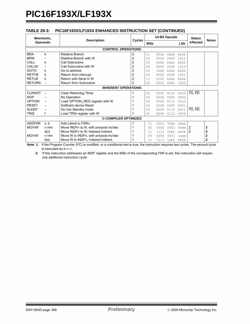
PIC16F193X/LF193X
TABLE 28-3: PIC16F193X/LF193X ENHANCED INSTRUCTION SET (CONTINUED)
Mnemonic,Operands
Description Cycles14-Bit Opcode Status
AffectedNotes
MSb LSb
CONTROL OPERATIONS
BRABRWCALLCALLWGOTORETFIERETLWRETURN
k–k–kkk–
Relative BranchRelative Branch with WCall SubroutineCall Subroutine with WGo to addressReturn from interruptReturn with literal in WReturn from Subroutine
22222222
1100100010001100
001k00000kkk00001kkk000001000000
kkkk0000kkkk0000kkkk0000kkkk0000
kkkk1011kkkk1010kkkk1001kkkk1000
INHERENT OPERATIONS
CLRWDTNOPOPTIONRESETSLEEPTRIS
–––––f
Clear Watchdog TimerNo OperationLoad OPTION_REG register with WSoftware device ResetGo into Standby modeLoad TRIS register with W
111111
000000000000
000000000000000000000000
011000000110000001100110
010000000010000100110fff
TO, PD
TO, PD
C-COMPILER OPTIMIZED
ADDFSRMOVIW
MOVWI
n, kn mmk[n]n mmk[n]
Add Literal to FSRnMove INDFn to W, with pre/post inc/dec Move INDFn to W, Indexed Indirect.Move W to INDFn, with pre/post inc/dec Move W to INDFn, Indexed Indirect.
11111
1100110011
00010000111100001111
0nkk00010nkk00011nkk
kkkk0nmmkkkk1nmmkkkk
ZZ
2222
Note 1: If the Program Counter (PC) is modified, or a conditional test is true, the instruction requires two cycles. The second cycle is executed as a NOP.
2: If this instruction addresses an INDF register and the MSb of the corresponding FSR is set, this instruction will require one additional instruction cycle.
DS41364D-page 368 Preliminary 2009 Microchip Technology Inc.
PIC16F193X/LF193X
28.2 Instruction Descriptions
ADDFSR Add Literal to FSRn
Syntax: [ label ] ADDFSR FSRn, k
Operands: -32 k 31n [ 0, 1]
Operation: FSR(n) + k FSR(n)
Status Affected: None
Description: The signed 6-bit literal ‘k’ is added to the contents of the FSRnH:FSRnL register pair.
FSRn is limited to the range 0000h - FFFFh. Moving beyond these bounds will cause the FSR to wrap around.
ADDLW Add literal and W
Syntax: [ label ] ADDLW k
Operands: 0 k 255
Operation: (W) + k (W)
Status Affected: C, DC, Z
Description: The contents of the W register are added to the eight-bit literal ‘k’ and the result is placed in the W register.
ADDWF Add W and f
Syntax: [ label ] ADDWF f,d
Operands: 0 f 127d 0,1
Operation: (W) + (f) (destination)
Status Affected: C, DC, Z
Description: Add the contents of the W register with register ‘f’. If ‘d’ is ‘0’, the result is stored in the W register. If ‘d’ is ‘1’, the result is stored back in register ‘f’.
ADDWFC ADD W and CARRY bit to f
Syntax: [ label ] ADDWFC f {,d}
Operands: 0 f 127d [0,1]
Operation: (W) + (f) + (C) dest
Status Affected: C, DC, Z
Description: Add W, the Carry flag and data mem-ory location ‘f’. If ‘d’ is ‘0’, the result is placed in W. If ‘d’ is ‘1’, the result is placed in data memory location ‘f’.
ANDLW AND literal with W
Syntax: [ label ] ANDLW k
Operands: 0 k 255
Operation: (W) .AND. (k) (W)
Status Affected: Z
Description: The contents of W register are AND’ed with the eight-bit literal ‘k’. The result is placed in the W register.
ANDWF AND W with f
Syntax: [ label ] ANDWF f,d
Operands: 0 f 127d 0,1
Operation: (W) .AND. (f) (destination)
Status Affected: Z
Description: AND the W register with register ‘f’. If ‘d’ is ‘0’, the result is stored in the W register. If ‘d’ is ‘1’, the result is stored back in register ‘f’.
ASRF Arithmetic Right Shift
Syntax: [ label ] ASRF f {,d}
Operands: 0 f 127d [0,1]
Operation: (f<7>) dest<7>(f<7:1>) dest<6:0>,(f<0>) C,
Status Affected: C, Z
Description: The contents of register ‘f’ are shifted one bit to the right through the Carry flag. The MSb remains unchanged. If ‘d’ is ‘0’, the result is placed in W. If ‘d’ is ‘1’, the result is stored back in reg-ister ‘f’.
register f C
2009 Microchip Technology Inc. Preliminary DS41364D-page 369

PIC16F193X/LF193X
BCF Bit Clear f
Syntax: [ label ] BCF f,b
Operands: 0 f 1270 b 7
Operation: 0 (f<b>)
Status Affected: None
Description: Bit ‘b’ in register ‘f’ is cleared.
BRA Relative Branch
Syntax: [ label ] BRA label [ label ] BRA $+k
Operands: -256 label - PC + 1 255-256 k 255
Operation: (PC) + 1 + k PC
Status Affected: None
Description: Add the signed 9-bit literal ‘k’ to the PC. Since the PC will have incre-mented to fetch the next instruction, the new address will be PC + 1 + k. This instruction is a two-cycle instruc-tion. This branch has a limited range.
BRW Relative Branch with W
Syntax: [ label ] BRW
Operands: None
Operation: (PC) + (W) PC
Status Affected: None
Description: Add the contents of W (unsigned) to the PC. Since the PC will have incre-mented to fetch the next instruction, the new address will be PC + 1 + (W). This instruction is a two-cycle instruc-tion.
BSF Bit Set f
Syntax: [ label ] BSF f,b
Operands: 0 f 1270 b 7
Operation: 1 (f<b>)
Status Affected: None
Description: Bit ‘b’ in register ‘f’ is set.
BTFSC Bit Test f, Skip if Clear
Syntax: [ label ] BTFSC f,b
Operands: 0 f 1270 b 7
Operation: skip if (f<b>) = 0
Status Affected: None
Description: If bit ‘b’ in register ‘f’ is ‘1’, the next instruction is executed.If bit ‘b’, in register ‘f’, is ‘0’, the next instruction is discarded, and a NOP is executed instead, making this a 2-cycle instruction.
BTFSS Bit Test f, Skip if Set
Syntax: [ label ] BTFSS f,b
Operands: 0 f 1270 b < 7
Operation: skip if (f<b>) = 1
Status Affected: None
Description: If bit ‘b’ in register ‘f’ is ‘0’, the next instruction is executed.If bit ‘b’ is ‘1’, then the nextinstruction is discarded and a NOP is executed instead, making this a 2-cycle instruction.
DS41364D-page 370 Preliminary 2009 Microchip Technology Inc.
PIC16F193X/LF193X
CALL Call Subroutine
Syntax: [ label ] CALL k
Operands: 0 k 2047
Operation: (PC)+ 1 TOS,k PC<10:0>,(PCLATH<4:3>) PC<12:11>
Status Affected: None
Description: Call Subroutine. First, return address (PC + 1) is pushed onto the stack. The eleven-bit immediate address is loaded into PC bits <10:0>. The upper bits of the PC are loaded from PCLATH. CALL is a two-cycle instruc-tion.
CALLW Subroutine Call With W
Syntax: [ label ] CALLW
Operands: None
Operation: (PC) +1 TOS,(W) PC<7:0>,(PCLATH<6:0>) PC<14:8>
Status Affected: None
Description: Subroutine call with W. First, the return address (PC + 1) is pushed onto the return stack. Then, the con-tents of W is loaded into PC<7:0>, and the contents of PCLATH into PC<14:8>. CALLW is a two-cycle instruction.
CLRF Clear f
Syntax: [ label ] CLRF f
Operands: 0 f 127
Operation: 00h (f)1 Z
Status Affected: Z
Description: The contents of register ‘f’ are cleared and the Z bit is set.
CLRW Clear W
Syntax: [ label ] CLRW
Operands: None
Operation: 00h (W)1 Z
Status Affected: Z
Description: W register is cleared. Zero bit (Z) is set.
CLRWDT Clear Watchdog Timer
Syntax: [ label ] CLRWDT
Operands: None
Operation: 00h WDT0 WDT prescaler,1 TO1 PD
Status Affected: TO, PD
Description: CLRWDT instruction resets the Watch-dog Timer. It also resets the prescaler of the WDT. Status bits TO and PD are set.
COMF Complement f
Syntax: [ label ] COMF f,d
Operands: 0 f 127d [0,1]
Operation: (f) (destination)
Status Affected: Z
Description: The contents of register ‘f’ are com-plemented. If ‘d’ is ‘0’, the result is stored in W. If ‘d’ is ‘1’, the result is stored back in register ‘f’.
DECF Decrement f
Syntax: [ label ] DECF f,d
Operands: 0 f 127d [0,1]
Operation: (f) - 1 (destination)
Status Affected: Z
Description: Decrement register ‘f’. If ‘d’ is ‘0’, the result is stored in the W register. If ‘d’ is ‘1’, the result is stored back in register ‘f’.
2009 Microchip Technology Inc. Preliminary DS41364D-page 371
PIC16F193X/LF193X
DECFSZ Decrement f, Skip if 0
Syntax: [ label ] DECFSZ f,d
Operands: 0 f 127d [0,1]
Operation: (f) - 1 (destination); skip if result = 0
Status Affected: None
Description: The contents of register ‘f’ are decre-mented. If ‘d’ is ‘0’, the result is placed in the W register. If ‘d’ is ‘1’, the result is placed back in register ‘f’. If the result is ‘1’, the next instruction is executed. If the result is ‘0’, then a NOP is executed instead, making it a 2-cycle instruction.
GOTO Unconditional Branch
Syntax: [ label ] GOTO k
Operands: 0 k 2047
Operation: k PC<10:0>PCLATH<4:3> PC<12:11>
Status Affected: None
Description: GOTO is an unconditional branch. The eleven-bit immediate value is loaded into PC bits <10:0>. The upper bits of PC are loaded from PCLATH<4:3>. GOTO is a two-cycle instruction.
INCF Increment f
Syntax: [ label ] INCF f,d
Operands: 0 f 127d [0,1]
Operation: (f) + 1 (destination)
Status Affected: Z
Description: The contents of register ‘f’ are incre-mented. If ‘d’ is ‘0’, the result is placed in the W register. If ‘d’ is ‘1’, the result is placed back in register ‘f’.
INCFSZ Increment f, Skip if 0
Syntax: [ label ] INCFSZ f,d
Operands: 0 f 127d [0,1]
Operation: (f) + 1 (destination), skip if result = 0
Status Affected: None
Description: The contents of register ‘f’ are incre-mented. If ‘d’ is ‘0’, the result is placed in the W register. If ‘d’ is ‘1’, the result is placed back in register ‘f’.If the result is ‘1’, the next instruction is executed. If the result is ‘0’, a NOP is executed instead, making it a 2-cycle instruction.
IORLW Inclusive OR literal with W
Syntax: [ label ] IORLW k
Operands: 0 k 255
Operation: (W) .OR. k (W)
Status Affected: Z
Description: The contents of the W register are OR’ed with the eight-bit literal ‘k’. The result is placed in the W register.
IORWF Inclusive OR W with f
Syntax: [ label ] IORWF f,d
Operands: 0 f 127d [0,1]
Operation: (W) .OR. (f) (destination)
Status Affected: Z
Description: Inclusive OR the W register with regis-ter ‘f’. If ‘d’ is ‘0’, the result is placed in the W register. If ‘d’ is ‘1’, the result is placed back in register ‘f’.
DS41364D-page 372 Preliminary 2009 Microchip Technology Inc.

PIC16F193X/LF193X
LSLF Logical Left Shift
Syntax: [ label ] LSLF f {,d}
Operands: 0 f 127d [0,1]
Operation: (f<7>) C(f<6:0>) dest<7:1>0 dest<0>
Status Affected: C, Z
Description: The contents of register ‘f’ are shifted one bit to the left through the Carry flag. A ‘0’ is shifted into the LSb. If ‘d’ is ‘0’, the result is placed in W. If ‘d’ is ‘1’, the result is stored back in register ‘f’.
LSRF Logical Right Shift
Syntax: [ label ] LSLF f {,d}
Operands: 0 f 127d [0,1]
Operation: 0 dest<7>(f<7:1>) dest<6:0>,(f<0>) C,
Status Affected: C, Z
Description: The contents of register ‘f’ are shifted one bit to the right through the Carry flag. A ‘0’ is shifted into the MSb. If ‘d’ is ‘0’, the result is placed in W. If ‘d’ is ‘1’, the result is stored back in register ‘f’.
register f 0C
register f C0
MOVF Move f
Syntax: [ label ] MOVF f,d
Operands: 0 f 127d [0,1]
Operation: (f) (dest)
Status Affected: Z
Description: The contents of register f is moved to a destination dependent upon the status of d. If d = 0,destination is W register. If d = 1, the destination is file register f itself. d = 1 is useful to test a file register since status flag Z is affected.
Words: 1
Cycles: 1
Example: MOVF FSR, 0
After InstructionW = value in FSR registerZ = 1
2009 Microchip Technology Inc. Preliminary DS41364D-page 373
PIC16F193X/LF193X
MOVIW Move INDFn to W
Syntax: [ label ] MOVIW ++INDFn[ label ] MOVIW --INDFn[ label ] MOVIW INDFn++[ label ] MOVIW INDFn--[ label ] MOVIW k[INDFn][ label ] MOVIW INDFn
Operands: n [0,1]mm [00, 01, 10, 11].-32 k 31If not present, k = 0.
Operation: INDFn WEffective address is determined by• FSR + 1 (preincrement)• FSR - 1 (predecrement)• FSR + k (relative offset)After the Move, the FSR value will be either:• FSR + 1 (all increments)• FSR - 1 (all decrements)• Unchanged
Status Affected: Z
mm Mode Syntax
00 Preincrement ++INDFn
01 Predecrement --INDFn
10 Postincrement INDFn++
11 Postdecrement INDFn--
Description: This instruction is used to move data between W and one of the indirect registers (INDFn). Before/after this move, the pointer (FSRn) is updated by pre/post incrementing/decrementing it.
Note: The INDFn registers are not physical registers. Any instruction that accesses an INDFn register actually accesses the register at the address specified by the FSRn.
FSRn is limited to the range 0000h - FFFFh. Incrementing/decrementing it beyond these bounds will cause it to wrap around.
The increment/decrement operation on FSRn WILL NOT affect any Status bits.
MOVLB Move literal to BSR
Syntax: [ label ] MOVLB k
Operands: 0 k 15
Operation: k BSR
Status Affected: None
Description: The five-bit literal ‘k’ is loaded into the Bank Select Register (BSR).
MOVLP Move literal to PCLATH
Syntax: [ label ] MOVLP k
Operands: 0 k 127
Operation: k PCLATH
Status Affected: None
Description: The seven-bit literal ‘k’ is loaded into the PCLATH register.
MOVLW Move literal to W
Syntax: [ label ] MOVLW k
Operands: 0 k 255
Operation: k (W)
Status Affected: None
Description: The eight-bit literal ‘k’ is loaded into W register. The “don’t cares” will assem-ble as ‘0’s.
Words: 1
Cycles: 1
Example: MOVLW 0x5A
After InstructionW = 0x5A
MOVWF Move W to f
Syntax: [ label ] MOVWF f
Operands: 0 f 127
Operation: (W) (f)
Status Affected: None
Description: Move data from W register to register ‘f’.
Words: 1
Cycles: 1
Example: MOVWF OPTION
Before InstructionOPTION = 0xFFW = 0x4F
After InstructionOPTION = 0x4FW = 0x4F
DS41364D-page 374 Preliminary 2009 Microchip Technology Inc.
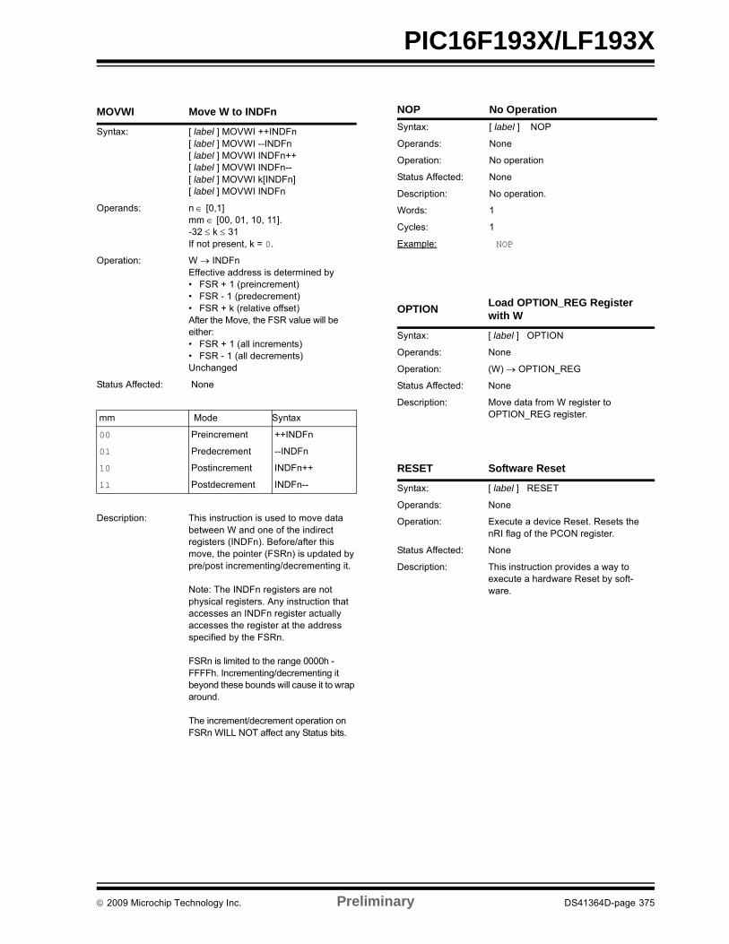
PIC16F193X/LF193X
MOVWI Move W to INDFn
Syntax: [ label ] MOVWI ++INDFn[ label ] MOVWI --INDFn[ label ] MOVWI INDFn++[ label ] MOVWI INDFn--[ label ] MOVWI k[INDFn][ label ] MOVWI INDFn
Operands: n [0,1]mm [00, 01, 10, 11].-32 k 31If not present, k = 0.
Operation: W INDFnEffective address is determined by• FSR + 1 (preincrement)• FSR - 1 (predecrement)• FSR + k (relative offset)After the Move, the FSR value will be either:• FSR + 1 (all increments)• FSR - 1 (all decrements)Unchanged
Status Affected: None
mm Mode Syntax
00 Preincrement ++INDFn
01 Predecrement --INDFn
10 Postincrement INDFn++
11 Postdecrement INDFn--
Description: This instruction is used to move data between W and one of the indirect registers (INDFn). Before/after this move, the pointer (FSRn) is updated by pre/post incrementing/decrementing it.
Note: The INDFn registers are not physical registers. Any instruction that accesses an INDFn register actually accesses the register at the address specified by the FSRn.
FSRn is limited to the range 0000h - FFFFh. Incrementing/decrementing it beyond these bounds will cause it to wrap around.
The increment/decrement operation on FSRn WILL NOT affect any Status bits.
NOP No Operation
Syntax: [ label ] NOP
Operands: None
Operation: No operation
Status Affected: None
Description: No operation.
Words: 1
Cycles: 1
Example: NOP
OPTIONLoad OPTION_REG Register with W
Syntax: [ label ] OPTION
Operands: None
Operation: (W) OPTION_REG
Status Affected: None
Description: Move data from W register to OPTION_REG register.
RESET Software Reset
Syntax: [ label ] RESET
Operands: None
Operation: Execute a device Reset. Resets the nRI flag of the PCON register.
Status Affected: None
Description: This instruction provides a way to execute a hardware Reset by soft-ware.
2009 Microchip Technology Inc. Preliminary DS41364D-page 375
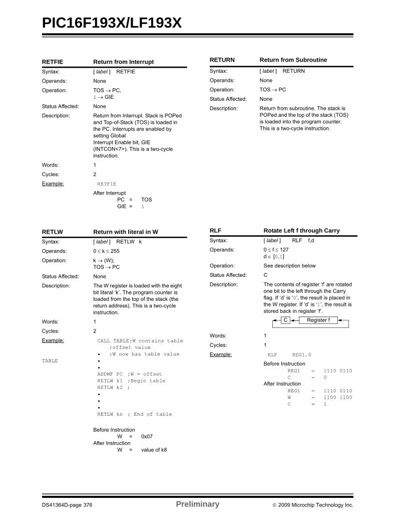
PIC16F193X/LF193X
RETFIE Return from Interrupt
Syntax: [ label ] RETFIE
Operands: None
Operation: TOS PC,1 GIE
Status Affected: None
Description: Return from Interrupt. Stack is POPed and Top-of-Stack (TOS) is loaded in the PC. Interrupts are enabled by setting GlobalInterrupt Enable bit, GIE (INTCON<7>). This is a two-cycle instruction.
Words: 1
Cycles: 2
Example: RETFIE
After InterruptPC = TOSGIE = 1
RETLW Return with literal in W
Syntax: [ label ] RETLW k
Operands: 0 k 255
Operation: k (W); TOS PC
Status Affected: None
Description: The W register is loaded with the eight bit literal ‘k’. The program counter is loaded from the top of the stack (the return address). This is a two-cycle instruction.
Words: 1
Cycles: 2
Example:
TABLE
CALL TABLE;W contains table;offset value
• ;W now has table value••ADDWF PC ;W = offsetRETLW k1 ;Begin tableRETLW k2 ;•••RETLW kn ; End of table
Before InstructionW = 0x07
After InstructionW = value of k8
RETURN Return from Subroutine
Syntax: [ label ] RETURN
Operands: None
Operation: TOS PC
Status Affected: None
Description: Return from subroutine. The stack is POPed and the top of the stack (TOS) is loaded into the program counter. This is a two-cycle instruction.
RLF Rotate Left f through Carry
Syntax: [ label ] RLF f,d
Operands: 0 f 127d [0,1]
Operation: See description below
Status Affected: C
Description: The contents of register ‘f’ are rotated one bit to the left through the Carry flag. If ‘d’ is ‘0’, the result is placed in the W register. If ‘d’ is ‘1’, the result is stored back in register ‘f’.
Words: 1
Cycles: 1
Example: RLF REG1,0
Before InstructionREG1 = 1110 0110C = 0
After InstructionREG1 = 1110 0110W = 1100 1100C = 1
Register fC
DS41364D-page 376 Preliminary 2009 Microchip Technology Inc.
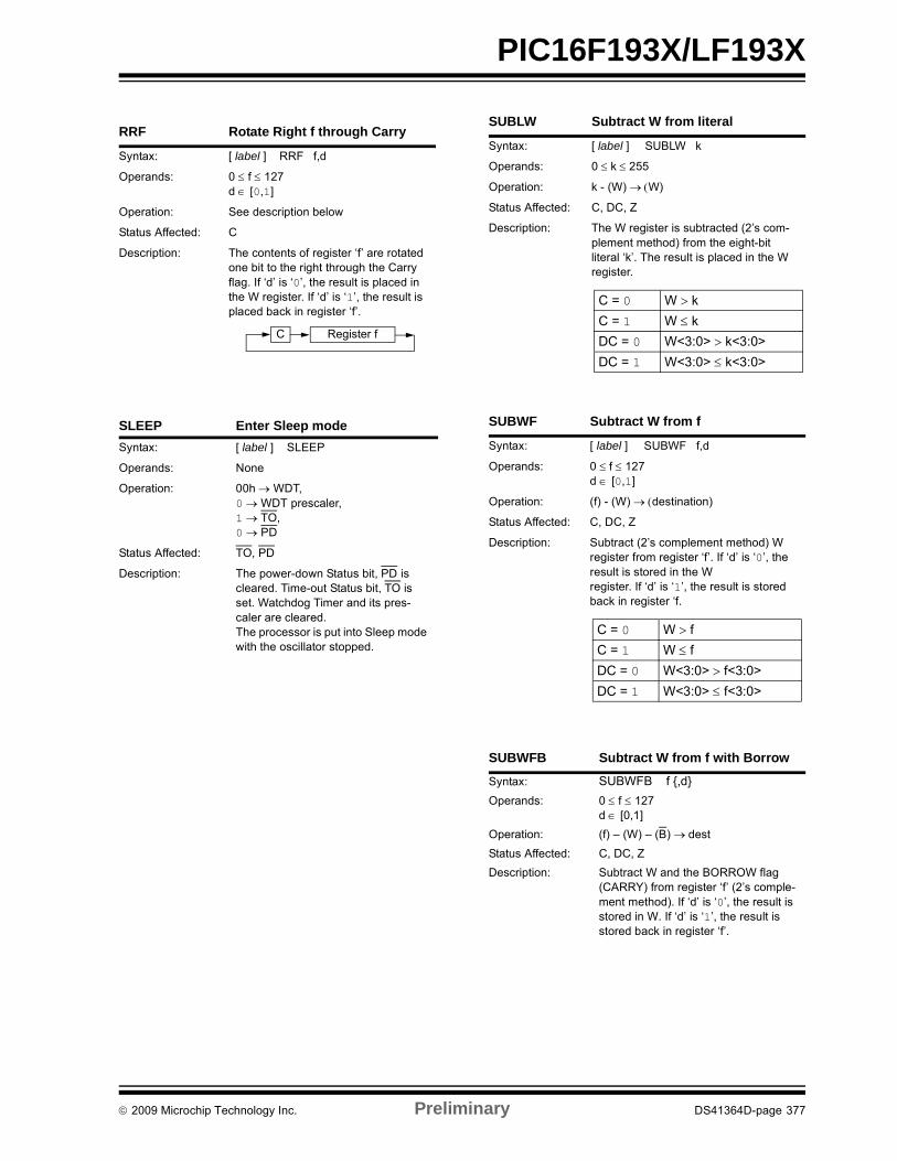
PIC16F193X/LF193X
RRF Rotate Right f through Carry
Syntax: [ label ] RRF f,d
Operands: 0 f 127d [0,1]
Operation: See description below
Status Affected: C
Description: The contents of register ‘f’ are rotated one bit to the right through the Carry flag. If ‘d’ is ‘0’, the result is placed in the W register. If ‘d’ is ‘1’, the result is placed back in register ‘f’.
SLEEP Enter Sleep mode
Syntax: [ label ] SLEEP
Operands: None
Operation: 00h WDT,0 WDT prescaler,1 TO,0 PD
Status Affected: TO, PD
Description: The power-down Status bit, PD is cleared. Time-out Status bit, TO is set. Watchdog Timer and its pres-caler are cleared.The processor is put into Sleep mode with the oscillator stopped.
Register fC
SUBLW Subtract W from literal
Syntax: [ label ] SUBLW k
Operands: 0 k 255
Operation: k - (W) W)
Status Affected: C, DC, Z
Description: The W register is subtracted (2’s com-plement method) from the eight-bit literal ‘k’. The result is placed in the W register.
SUBWF Subtract W from f
Syntax: [ label ] SUBWF f,d
Operands: 0 f 127d [0,1]
Operation: (f) - (W) destination)
Status Affected: C, DC, Z
Description: Subtract (2’s complement method) W register from register ‘f’. If ‘d’ is ‘0’, the result is stored in the W register. If ‘d’ is ‘1’, the result is stored back in register ‘f.
SUBWFB Subtract W from f with Borrow
Syntax: SUBWFB f {,d}
Operands: 0 f 127d [0,1]
Operation: (f) – (W) – (B) dest
Status Affected: C, DC, Z
Description: Subtract W and the BORROW flag (CARRY) from register ‘f’ (2’s comple-ment method). If ‘d’ is ‘0’, the result is stored in W. If ‘d’ is ‘1’, the result is stored back in register ‘f’.
C = 0 W k
C = 1 W k
DC = 0 W<3:0> k<3:0>
DC = 1 W<3:0> k<3:0>
C = 0 W f
C = 1 W f
DC = 0 W<3:0> f<3:0>
DC = 1 W<3:0> f<3:0>
2009 Microchip Technology Inc. Preliminary DS41364D-page 377
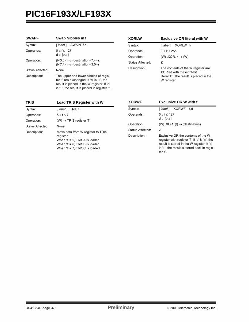
PIC16F193X/LF193X
SWAPF Swap Nibbles in f
Syntax: [ label ] SWAPF f,d
Operands: 0 f 127d [0,1]
Operation: (f<3:0>) (destination<7:4>),(f<7:4>) (destination<3:0>)
Status Affected: None
Description: The upper and lower nibbles of regis-ter ‘f’ are exchanged. If ‘d’ is ‘0’, the result is placed in the W register. If ‘d’ is ‘1’, the result is placed in register ‘f’.
TRIS Load TRIS Register with W
Syntax: [ label ] TRIS f
Operands: 5 f 7
Operation: (W) TRIS register ‘f’
Status Affected: None
Description: Move data from W register to TRIS register.When ‘f’ = 5, TRISA is loaded.When ‘f’ = 6, TRISB is loaded.When ‘f’ = 7, TRISC is loaded.
XORLW Exclusive OR literal with W
Syntax: [ label ] XORLW k
Operands: 0 k 255
Operation: (W) .XOR. k W)
Status Affected: Z
Description: The contents of the W register are XOR’ed with the eight-bitliteral ‘k’. The result is placed in the W register.
XORWF Exclusive OR W with f
Syntax: [ label ] XORWF f,d
Operands: 0 f 127d [0,1]
Operation: (W) .XOR. (f) destination)
Status Affected: Z
Description: Exclusive OR the contents of the W register with register ‘f’. If ‘d’ is ‘0’, the result is stored in the W register. If ‘d’ is ‘1’, the result is stored back in regis-ter ‘f’.
DS41364D-page 378 Preliminary 2009 Microchip Technology Inc.
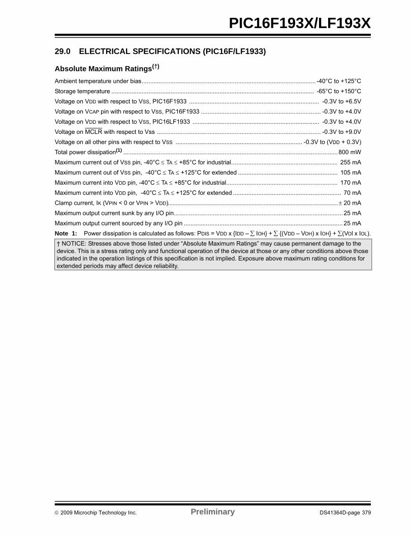
PIC16F193X/LF193X
29.0 ELECTRICAL SPECIFICATIONS (PIC16F/LF1933)
Absolute Maximum Ratings(†)
Ambient temperature under bias....................................................................................................... -40°C to +125°C
Storage temperature ........................................................................................................................ -65°C to +150°C
Voltage on VDD with respect to VSS, PIC16F1933 ............................................................................. -0.3V to +6.5V
Voltage on VCAP pin with respect to VSS, PIC16F1933 ....................................................................... -0.3V to +4.0V
Voltage on VDD with respect to VSS, PIC16LF1933 ........................................................................... -0.3V to +4.0V
Voltage on MCLR with respect to Vss ................................................................................................. -0.3V to +9.0V
Voltage on all other pins with respect to VSS ........................................................................... -0.3V to (VDD + 0.3V)
Total power dissipation(1) ............................................................................................................................... 800 mW
Maximum current out of VSS pin, -40°C TA +85°C for industrial............................................................... 255 mA
Maximum current out of VSS pin, -40°C TA +125°C for extended ........................................................... 105 mA
Maximum current into VDD pin, -40°C TA +85°C for industrial.................................................................. 170 mA
Maximum current into VDD pin, -40°C TA +125°C for extended ................................................................ 70 mA
Clamp current, IK (VPIN < 0 or VPIN > VDD)20 mA
Maximum output current sunk by any I/O pin.................................................................................................... 25 mA
Maximum output current sourced by any I/O pin .............................................................................................. 25 mA
Note 1: Power dissipation is calculated as follows: PDIS = VDD x {IDD – IOH} + {(VDD – VOH) x IOH} + (VOl x IOL).
† NOTICE: Stresses above those listed under “Absolute Maximum Ratings” may cause permanent damage to the device. This is a stress rating only and functional operation of the device at those or any other conditions above those indicated in the operation listings of this specification is not implied. Exposure above maximum rating conditions for extended periods may affect device reliability.
2009 Microchip Technology Inc. Preliminary DS41364D-page 379
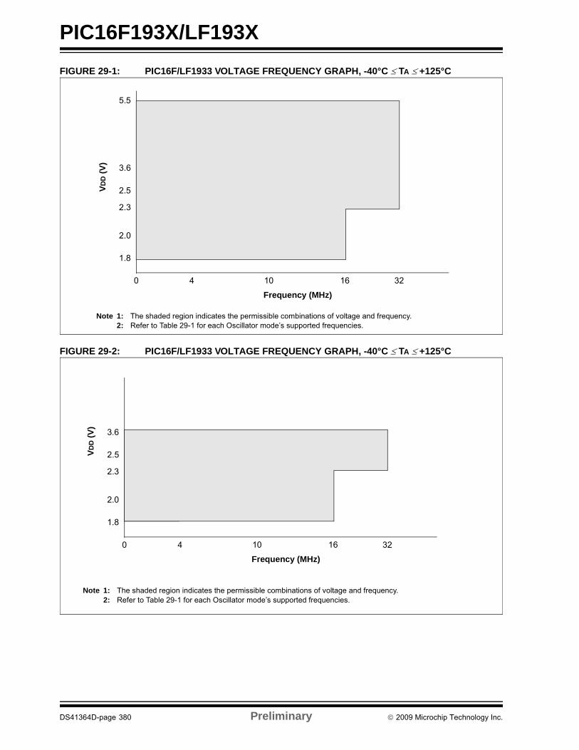
PIC16F193X/LF193X
FIGURE 29-1: PIC16F/LF1933 VOLTAGE FREQUENCY GRAPH, -40°C TA +125°C
FIGURE 29-2: PIC16F/LF1933 VOLTAGE FREQUENCY GRAPH, -40°C TA +125°C
1.8
2.5
2.0
0
2.3
Frequency (MHz)
VD
D (
V)
Note 1: The shaded region indicates the permissible combinations of voltage and frequency.2: Refer to Table 29-1 for each Oscillator mode’s supported frequencies.
4 3210 16
5.5
3.6
1.8
2.5
2.0
0
2.3
Frequency (MHz)
VD
D (
V)
Note 1: The shaded region indicates the permissible combinations of voltage and frequency.2: Refer to Table 29-1 for each Oscillator mode’s supported frequencies.
4 3210 16
3.6
DS41364D-page 380 Preliminary 2009 Microchip Technology Inc.
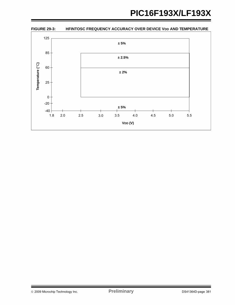
PIC16F193X/LF193X
FIGURE 29-3: HFINTOSC FREQUENCY ACCURACY OVER DEVICE VDD AND TEMPERATURE
125
25
2.0
0
60
85
VDD (V)
4.0 5.04.5
Tem
pe
ratu
re (
°C)
2.5 3.0 3.5 5.51.8-40
-20
± 5%
± 2%
± 5%
± 2.5%
2009 Microchip Technology Inc. Preliminary DS41364D-page 381

PIC16F193X/LF193X
29.1 DC Characteristics: PIC16F/LF1933-I/E (Industrial, Extended)
PIC16LF1933Standard Operating Conditions (unless otherwise stated)Operating temperature -40°C TA +85°C for industrial
-40°C TA +125°C for extended
PIC16F1933Standard Operating Conditions (unless otherwise stated)Operating temperature -40°C TA +85°C for industrial
-40°C TA +125°C for extended
Param. No.
Sym. Characteristic Min. Typ† Max. Units Conditions
D001 VDD Supply Voltage
PIC16LF1933 1.82.3
——
3.63.6
VV
FOSC 16 MHz:FOSC 32 MHz (NOTE 2)
D001 PIC16F1933 1.82.3
——
5.55.5
VV
FOSC 16 MHz:FOSC 32 MHz (NOTE 2)
D002* VDR RAM Data Retention Voltage(1)
PIC16LF1933 1.5 — — V Device in Sleep mode
D002* PIC16F1933 1.7 — — V Device in Sleep mode
VPOR* Power-on Reset Release Voltage — 1.6 — V
VPORR* Power-on Reset Rearm Voltage
PIC16LF1933 — 0.8 — V Device in Sleep mode
PIC16F1933 — 1.7 — V Device in Sleep mode
D003 VADFVR Fixed Voltage Reference Voltage for ADC, Initial Accuracy
-6-7-7-8-7-8
——————
446644
% 1.024V, VDD 1.8V, 85°C1.024V, VDD 1.8V, 125°C2.048V, VDD 2.5V, 85°C2.048V, VDD 2.5V, 125°C4.096V, VDD 4.75V, 85°C4.096V, VDD 4.75V, 125°C
D003A VCDAFVR Fixed Voltage Reference Voltage for Comparator and DAC, Initial Accuracy
-7-8-8-9-8-8
——————
557744
% 1.024V, VDD 1.8V, 85°C1.024V, VDD 1.8V, 125°C2.048V, VDD 2.5V, 85°C2.048V, VDD 2.5V, 125°C4.096V, VDD 4.75V, 85°C4.096V, VDD 4.75V, 125°C
D003B VLCDFVR Fixed Voltage Reference Voltage for LCD Bias, Initial Accuracy
-9-9.5
——
99
% 3.072V, VDD 3.6V, 85°C3.072V, VDD 3.6V, 125°C
D003C* TCVFVR Temperature Coefficient, Fixed Voltage Reference
— -130 — ppm/°C
D003D* VFVR/VIN
Line Regulation, Fixed Voltage Ref-erence
— 0.270 — %/V
D004* SVDD VDD Rise Rate to ensure internal Power-on Reset signal
0.05 — — V/ms See Section 6.1 “Power-on Reset (POR)” for details.
* These parameters are characterized but not tested.† Data in “Typ” column is at 3.3V, 25°C unless otherwise stated. These parameters are for design guidance only and are not
tested.
Note 1: This is the limit to which VDD can be lowered in Sleep mode without losing RAM data.2: PLL required for 32 MHz operation.
DS41364D-page 382 Preliminary 2009 Microchip Technology Inc.

PIC16F193X/LF193X
FIGURE 29-4: POR AND POR REARM WITH SLOW RISING VDD
VDD
VPOR
VPORR
VSS
VSS
NPOR
TPOR(3)
POR REARM
Note 1: When NPOR is low, the device is held in Reset.2: TPOR 1 s typical.3: TVLOW 2.7 s typical.
TVLOW(2)
2009 Microchip Technology Inc. Preliminary DS41364D-page 383

PIC16F193X/LF193X
29.2 DC Characteristics: PIC16F/LF1933-I/E (Industrial, Extended)
PIC16LF1933Standard Operating Conditions (unless otherwise stated)Operating temperature -40°C TA +85°C for industrial
-40°C TA +125°C for extended
PIC16F1933Standard Operating Conditions (unless otherwise stated)Operating temperature -40°C TA +85°C for industrial
-40°C TA +125°C for extended
ParamNo.
Device Characteristics
Min. Typ† Max. UnitsConditions
VDD Note
Supply Current (IDD)(1, 2)
D009 LDO Regulator — 350 — A — HS, EC OR INTOSC/INTOSCIO (8-16 MHZ) Clock modes with all VCAP pins disabled
— 50 — A — All VCAP pins disabled
— 30 — A — VCAP enabled on RA0, RA5 or RA6
— 5 — A — LP Clock mode and Sleep (requires FVR and BOR to be disabled)
D010 — 8 14 A 1.8 FOSC = 32 kHzLP Oscillator mode (Note 4),-40°C TA +85°C
— 12 18 A 3.0
D010 — 23 38 A 1.8 FOSC = 32 kHzLP Oscillator mode (Note 4, 5),-40°C TA +85°C
— 28 43 A 3.0
— 33 48 A 5.0
D010A — 10 18 A 1.8 FOSC = 32 kHzLP Oscillator mode (Note 4)-40°C TA +125°C
— 15 20 A 3.0
D010A — 24 42 A 1.8 FOSC = 32 kHzLP Oscillator mode (Note 4, 5)-40°C TA +125°C
— 30 44 A 3.0
— 35 50 A 5.0
D011 — 125 175 A 1.8 FOSC = 1 MHzXT Oscillator mode— 200 300 A 3.0
D011 — 135 200 A 1.8 FOSC = 1 MHzXT Oscillator mode (Note 5)— 210 450 A 3.0
— 350 650 A 5.0
D012 — 300 400 A 1.8 FOSC = 4 MHzXT Oscillator mode— 550 700 A 3.0
D012 — 320 550 A 1.8 FOSC = 4 MHzXT Oscillator mode (Note 5)— 570 800 A 3.0
— 700 960 A 5.0
Note 1: The test conditions for all IDD measurements in active operation mode are: OSC1 = external square wave, from rail-to-rail; all I/O pins tri-stated, pulled to VDD; MCLR = VDD; WDT disabled.
2: The supply current is mainly a function of the operating voltage and frequency. Other factors, such as I/O pin loading and switching rate, oscillator type, internal code execution pattern and temperature, also have an impact on the current consumption.
3: For RC oscillator configurations, current through REXT is not included. The current through the resistor can be extended by the formula IR = VDD/2REXT (mA) with REXT in k
4: FVR and BOR are disabled.5: 0.1 F capacitor on VCAP (RA0).6: 8 MHz crystal oscillator with 4x PLL enabled.
DS41364D-page 384 Preliminary 2009 Microchip Technology Inc.
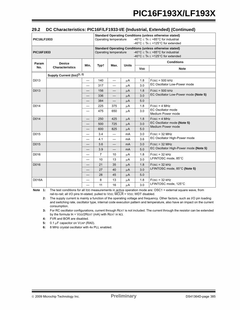
PIC16F193X/LF193X
Supply Current (IDD)(1, 2)
D013 — 140 — A 1.8 FOSC = 500 kHzEC Oscillator Low-Power mode— 317 — A 3.0
D013 — 156 — A 1.8 FOSC = 500 kHzEC Oscillator Low-Power mode (Note 5)— 336 — A 3.0
— 384 — A 5.0
D014 — 225 375 A 1.8 FOSC = 4 MHzEC Oscillator modeMedium Power mode
— 475 650 A 3.0
D014 — 250 425 A 1.8 FOSC = 4 MHzEC Oscillator mode (Note 5)Medium Power mode
— 500 725 A 3.0
— 600 825 A 5.0
D015 — 3.4 — mA 3.0 FOSC = 32 MHzEC Oscillator High-Power mode— 4.1 — mA 3.6
D015 — 3.6 — mA 3.0 FOSC = 32 MHzEC Oscillator High-Power mode (Note 5)— 3.9 — mA 5.0
D016 — 7 10 A 1.8 FOSC = 32 kHzLFINTOSC mode, 85°C— 10 13 A 3.0
D016 — 21 35 A 1.8 FOSC = 32 kHzLFINTOSC mode, 85°C (Note 5)— 27 40 A 3.0
— 28 45 A 5.0
D016A — 8 13 A 1.8 FOSC = 32 kHzLFINTOSC mode, 125°C— 11 16 A 3.0
29.2 DC Characteristics: PIC16F/LF1933-I/E (Industrial, Extended) (Continued)
PIC16LF1933Standard Operating Conditions (unless otherwise stated)Operating temperature -40°C TA +85°C for industrial
-40°C TA +125°C for extended
PIC16F1933Standard Operating Conditions (unless otherwise stated)Operating temperature -40°C TA +85°C for industrial
-40°C TA +125°C for extended
ParamNo.
Device Characteristics
Min. Typ† Max. UnitsConditions
VDD Note
Note 1: The test conditions for all IDD measurements in active operation mode are: OSC1 = external square wave, from rail-to-rail; all I/O pins tri-stated, pulled to VDD; MCLR = VDD; WDT disabled.
2: The supply current is mainly a function of the operating voltage and frequency. Other factors, such as I/O pin loading and switching rate, oscillator type, internal code execution pattern and temperature, also have an impact on the current consumption.
3: For RC oscillator configurations, current through REXT is not included. The current through the resistor can be extended by the formula IR = VDD/2REXT (mA) with REXT in k
4: FVR and BOR are disabled.5: 0.1 F capacitor on VCAP (RA0).6: 8 MHz crystal oscillator with 4x PLL enabled.
2009 Microchip Technology Inc. Preliminary DS41364D-page 385

PIC16F193X/LF193X
D017Supply Current (IDD)(1, 2)
— 130 175 A 1.8 FOSC = 500 kHzMFINTOSC mode— 190 250 A 3.0
D017 — 150 250 A 1.8 FOSC = 500 kHzMFINTOSC mode (Note 5)— 210 345 A 3.0
— 270 425 A 5.0
D018 — 800 1100 A 1.8 FOSC = 8 MHzHFINTOSC mode— 1300 1700 A 3.0
D018 — 0.85 1.2 mA 1.8 FOSC = 8 MHzHFINTOSC mode (Note 5)— 1.4 1.9 mA 3.0
— 1.6 2.2 mA 5.0
D019 — 1.25 1.75 mA 1.8 FOSC = 16 MHzHFINTOSC mode— 2.0 2.5 mA 3.0
D019 — 1.4 2.0 mA 1.8 FOSC = 16 MHzHFINTOSC mode (Note 5)— 2.2 2.8 mA 3.0
— 2.4 3.0 mA 5.0
D020 — 300 450 A 1.8 FOSC = 4 MHzEXTRC mode (Note 3, Note 5)— 500 700 A 3.0
D020 — 350 600 A 1.8 FOSC = 4 MHzEXTRC mode (Note 3, Note 5)— 550 900 A 3.0
— 620 1000 A 5.0
D021 — 3.4 — mA 3.0 FOSC = 32 MHzHS Oscillator mode (Note 6)— 4.2 — mA 3.6
D021 — 3.6 — mA 3.0 FOSC = 32 MHzHS Oscillator mode (Note 5, Note 6)— 3.9 — mA 5.0
29.2 DC Characteristics: PIC16F/LF1933-I/E (Industrial, Extended) (Continued)
PIC16LF1933Standard Operating Conditions (unless otherwise stated)Operating temperature -40°C TA +85°C for industrial
-40°C TA +125°C for extended
PIC16F1933Standard Operating Conditions (unless otherwise stated)Operating temperature -40°C TA +85°C for industrial
-40°C TA +125°C for extended
ParamNo.
Device Characteristics
Min. Typ† Max. UnitsConditions
VDD Note
Note 1: The test conditions for all IDD measurements in active operation mode are: OSC1 = external square wave, from rail-to-rail; all I/O pins tri-stated, pulled to VDD; MCLR = VDD; WDT disabled.
2: The supply current is mainly a function of the operating voltage and frequency. Other factors, such as I/O pin loading and switching rate, oscillator type, internal code execution pattern and temperature, also have an impact on the current consumption.
3: For RC oscillator configurations, current through REXT is not included. The current through the resistor can be extended by the formula IR = VDD/2REXT (mA) with REXT in k
4: FVR and BOR are disabled.5: 0.1 F capacitor on VCAP (RA0).6: 8 MHz crystal oscillator with 4x PLL enabled.
DS41364D-page 386 Preliminary 2009 Microchip Technology Inc.

PIC16F193X/LF193X
29.3 DC Characteristics: PIC16F/LF1933-I/E (Power-Down)
PIC16LF1933Standard Operating Conditions (unless otherwise stated)Operating temperature -40°C TA +85°C for industrial
-40°C TA +125°C for extended
PIC16F1933Standard Operating Conditions (unless otherwise stated)Operating temperature -40°C TA +85°C for industrial
-40°C TA +125°C for extended
ParamNo.
Device Characteristics Min. Typ†Max.
+85°CMax.
+125°CUnits
Conditions
VDD Note
Power-down Base Current (IPD)(2)
D023 — 0.06 1 — A 1.8 WDT, BOR, FVR, and T1OSC disabled, all Peripherals Inactive— 0.08 2 — A 3.0
D023 — 15 35 — A 1.8 WDT, BOR, FVR, and T1OSC disabled, all Peripherals Inactive— 18 40 — A 3.0
— 19 45 — A 5.0
D024 — 0.5 6 — A 1.8 LPWDT Current (Note 1)
— 0.8 7 — A 3.0
D024 — 16 35 — A 1.8 LPWDT Current (Note 1)
— 19 40 — A 3.0
— 20 45 — A 5.0
D025 — 8.5 23 — A 1.8 FVR current
— 8.5 26 — A 3.0
D025 — 32 50 — A 1.8 FVR current (Note 4)
— 39 72 — A 3.0
— 70 120 — A 5.0
D026 — 7.5 TBD — A 3.0 BOR Current (Note 1)
D026 — 34 57 — A 3.0 BOR Current (Note 1, Note 4)
— 67 100 — A 5.0
D027 — 0.6 5 — A 1.8 T1OSC Current (Note 1)
— 1.8 6 — A 3.0
D027 — 16 35 — A 1.8 T1OSC Current (Note 1)
— 21 40 — A 3.0
— 25 45 — A 5.0
* These parameters are characterized but not tested.† Data in “Typ” column is at 3.0V, 25°C unless otherwise stated. These parameters are for design guidance only and are
not tested.Legend: TBD = To Be DeterminedNote 1: The peripheral current is the sum of the base IDD or IPD and the additional current consumed when this peripheral is
enabled. The peripheral current can be determined by subtracting the base IDD or IPD current from this limit. Max values should be used when calculating total current consumption.
2: The power-down current in Sleep mode does not depend on the oscillator type. Power-down current is measured with the part in Sleep mode, with all I/O pins in high-impedance state and tied to VDD.
3: A/D oscillator source is FRC.4: 0.1 F capacitor on VCAP (RA0).
2009 Microchip Technology Inc. Preliminary DS41364D-page 387
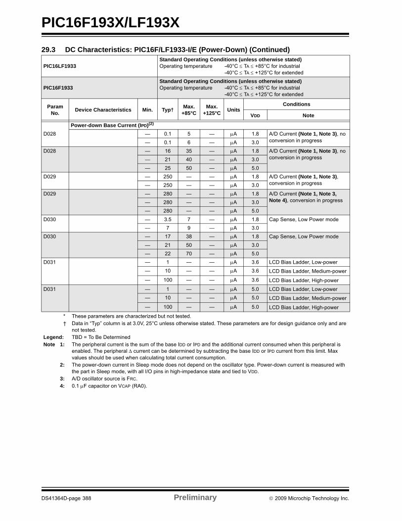
PIC16F193X/LF193X
Power-down Base Current (IPD)(2)
D028 — 0.1 5 — A 1.8 A/D Current (Note 1, Note 3), no conversion in progress— 0.1 6 — A 3.0
D028 — 16 35 — A 1.8 A/D Current (Note 1, Note 3), no conversion in progress— 21 40 — A 3.0
— 25 50 — A 5.0
D029 — 250 — — A 1.8 A/D Current (Note 1, Note 3), conversion in progress— 250 — — A 3.0
D029 — 280 — — A 1.8 A/D Current (Note 1, Note 3, Note 4), conversion in progress— 280 — — A 3.0
— 280 — — A 5.0
D030 — 3.5 7 — A 1.8 Cap Sense, Low Power mode
— 7 9 — A 3.0
D030 — 17 38 — A 1.8 Cap Sense, Low Power mode
— 21 50 — A 3.0
— 22 70 — A 5.0
D031 — 1 — — A 3.6 LCD Bias Ladder, Low-power
— 10 — — A 3.6 LCD Bias Ladder, Medium-power
— 100 — — A 3.6 LCD Bias Ladder, High-power
D031 — 1 — — A 5.0 LCD Bias Ladder, Low-power
— 10 — — A 5.0 LCD Bias Ladder, Medium-power
— 100 — — A 5.0 LCD Bias Ladder, High-power
29.3 DC Characteristics: PIC16F/LF1933-I/E (Power-Down) (Continued)
PIC16LF1933Standard Operating Conditions (unless otherwise stated)Operating temperature -40°C TA +85°C for industrial
-40°C TA +125°C for extended
PIC16F1933Standard Operating Conditions (unless otherwise stated)Operating temperature -40°C TA +85°C for industrial
-40°C TA +125°C for extended
ParamNo.
Device Characteristics Min. Typ†Max.
+85°CMax.
+125°CUnits
Conditions
VDD Note
* These parameters are characterized but not tested.† Data in “Typ” column is at 3.0V, 25°C unless otherwise stated. These parameters are for design guidance only and are
not tested.Legend: TBD = To Be DeterminedNote 1: The peripheral current is the sum of the base IDD or IPD and the additional current consumed when this peripheral is
enabled. The peripheral current can be determined by subtracting the base IDD or IPD current from this limit. Max values should be used when calculating total current consumption.
2: The power-down current in Sleep mode does not depend on the oscillator type. Power-down current is measured with the part in Sleep mode, with all I/O pins in high-impedance state and tied to VDD.
3: A/D oscillator source is FRC.4: 0.1 F capacitor on VCAP (RA0).
DS41364D-page 388 Preliminary 2009 Microchip Technology Inc.
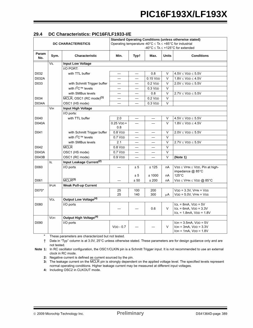
PIC16F193X/LF193X
29.4 DC Characteristics: PIC16F/LF1933-I/E
DC CHARACTERISTICSStandard Operating Conditions (unless otherwise stated)Operating temperature -40°C TA +85°C for industrial
-40°C TA +125°C for extended
ParamNo.
Sym. Characteristic Min. Typ† Max. Units Conditions
VIL Input Low Voltage
I/O PORT:
D032 with TTL buffer — — 0.8 V 4.5V VDD 5.5V
D032A — — 0.15 VDD V 1.8V VDD 4.5V
D033 with Schmitt Trigger buffer — — 0.2 VDD V 2.0V VDD 5.5V
with I2C™ levels — — 0.3 VDD V
with SMBus levels — — 0.8 V 2.7V VDD 5.5V
D034 MCLR, OSC1 (RC mode)(1) — — 0.2 VDD V
D034A OSC1 (HS mode) — — 0.3 VDD V
VIH Input High Voltage
I/O ports:
D040 with TTL buffer 2.0 — — V 4.5V VDD 5.5V
D040A 0.25 VDD + 0.8
— — V 1.8V VDD 4.5V
D041 with Schmitt Trigger buffer 0.8 VDD — — V 2.0V VDD 5.5V
with I2C™ levels 0.7 VDD — — V
with SMBus levels 2.1 — — V 2.7V VDD 5.5V
D042 MCLR 0.8 VDD — — V
D043A OSC1 (HS mode) 0.7 VDD — — V
D043B OSC1 (RC mode) 0.9 VDD — — V (Note 1)
IIL Input Leakage Current(2)
D060 I/O ports — ± 5
± 5
± 125
± 1000
nA
nA
VSS VPIN VDD, Pin at high-impedance @ 85°C125°C
D061 MCLR(3) — ± 50 ± 200 nA VSS VPIN VDD @ 85°C
IPUR Weak Pull-up Current
D070* 2525
100140
200300 A
VDD = 3.3V, VPIN = VSS
VDD = 5.0V, VPIN = VSS
VOL Output Low Voltage(4)
D080 I/O ports— — 0.6 V
IOL = 8mA, VDD = 5VIOL = 6mA, VDD = 3.3VIOL = 1.8mA, VDD = 1.8V
VOH Output High Voltage(4)
D090 I/O portsVDD - 0.7 — — V
IOH = 3.5mA, VDD = 5VIOH = 3mA, VDD = 3.3VIOH = 1mA, VDD = 1.8V
* These parameters are characterized but not tested.† Data in “Typ” column is at 3.0V, 25°C unless otherwise stated. These parameters are for design guidance only and are
not tested.Note 1: In RC oscillator configuration, the OSC1/CLKIN pin is a Schmitt Trigger input. It is not recommended to use an external
clock in RC mode.2: Negative current is defined as current sourced by the pin.3: The leakage current on the MCLR pin is strongly dependent on the applied voltage level. The specified levels represent
normal operating conditions. Higher leakage current may be measured at different input voltages.4: Including OSC2 in CLKOUT mode.
2009 Microchip Technology Inc. Preliminary DS41364D-page 389
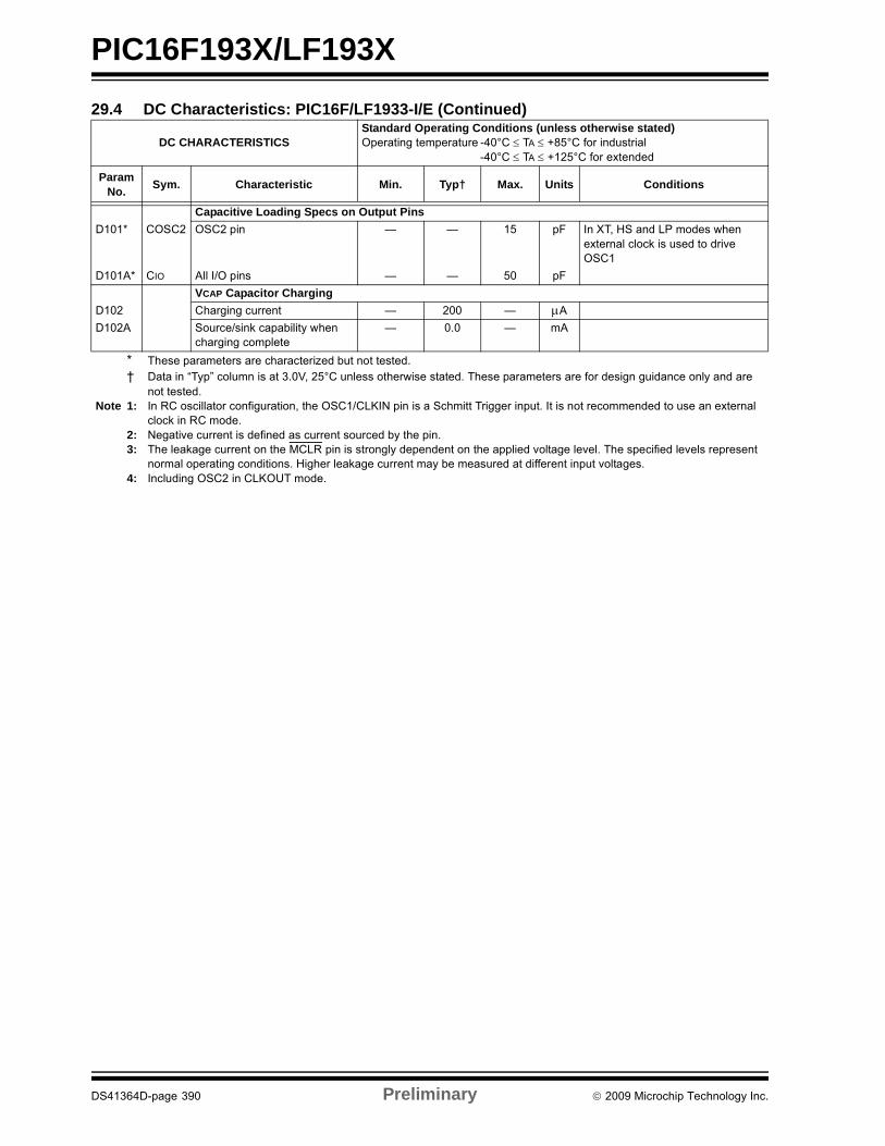
PIC16F193X/LF193X
Capacitive Loading Specs on Output Pins
D101* COSC2 OSC2 pin — — 15 pF In XT, HS and LP modes when external clock is used to drive OSC1
D101A* CIO All I/O pins — — 50 pF
VCAP Capacitor Charging
D102 Charging current — 200 — A
D102A Source/sink capability when charging complete
— 0.0 — mA
29.4 DC Characteristics: PIC16F/LF1933-I/E (Continued)
DC CHARACTERISTICSStandard Operating Conditions (unless otherwise stated)Operating temperature -40°C TA +85°C for industrial
-40°C TA +125°C for extended
ParamNo.
Sym. Characteristic Min. Typ† Max. Units Conditions
* These parameters are characterized but not tested.† Data in “Typ” column is at 3.0V, 25°C unless otherwise stated. These parameters are for design guidance only and are
not tested.Note 1: In RC oscillator configuration, the OSC1/CLKIN pin is a Schmitt Trigger input. It is not recommended to use an external
clock in RC mode.2: Negative current is defined as current sourced by the pin.3: The leakage current on the MCLR pin is strongly dependent on the applied voltage level. The specified levels represent
normal operating conditions. Higher leakage current may be measured at different input voltages.4: Including OSC2 in CLKOUT mode.
DS41364D-page 390 Preliminary 2009 Microchip Technology Inc.

PIC16F193X/LF193X
29.5 Memory Programming Requirements
DC CHARACTERISTICSStandard Operating Conditions (unless otherwise stated)Operating temperature -40°C TA +125°C
ParamNo.
Sym. Characteristic Min. Typ† Max. Units Conditions
Program Memory Programming Specifications
D110 VIHH Voltage on MCLR/VPP/RE3 pin 8.0 — 9.0 V (Note 3, Note 4)
D111 IDDP Supply Current during Programming
— — 10 mA
D112 VDD for Bulk Erase 2.7 — VDD
max.V
D113 VPEW VDD for Write or Row Erase VDD
min.— VDD
max.V
D114 IPPPGM Current on MCLR/VPP during Erase/Write
— — 1.0 mA
D115 IDDPGM Current on VDD during Erase/Write — 5.0 mA
Data EEPROM Memory
D116 ED Byte Endurance 100K — — E/W -40C to +85C
D117 VDRW VDD for Read/Write VDD
min.— VDD
max.V
D118 TDEW Erase/Write Cycle Time — 4.0 5.0 ms
D119 TRETD Characteristic Retention 40 — — Year Provided no other specifications are violated
D120 TREF Number of Total Erase/Write Cycles before Refresh(2)
1M 10M — E/W -40°C to +85°C
Program Flash Memory
D121 EP Cell Endurance 10K — — E/W -40C to +85C (Note 1)
D122 VPR VDD for Read VDD
min.— VDD
max.V
D123 TIW Self-timed Write Cycle Time — 2 2.5 ms
D124 TRETD Characteristic Retention 40 — — Year Provided no other specifications are violated
† Data in “Typ” column is at 3.0V, 25°C unless otherwise stated. These parameters are for design guidance only and are not tested.
Note 1: Self-write and Block Erase.2: Refer to Section 11.2 “Using the Data EEPROM” for a more detailed discussion on data EEPROM
endurance.3: Required only if single-supply programming is disabled.4: The MPLAB ICD 2 does not support variable VPP output. Circuitry to limit the ICD 2 VPP voltage must be
placed between the ICD 2 and target system when programming or debugging with the ICD 2.
2009 Microchip Technology Inc. Preliminary DS41364D-page 391
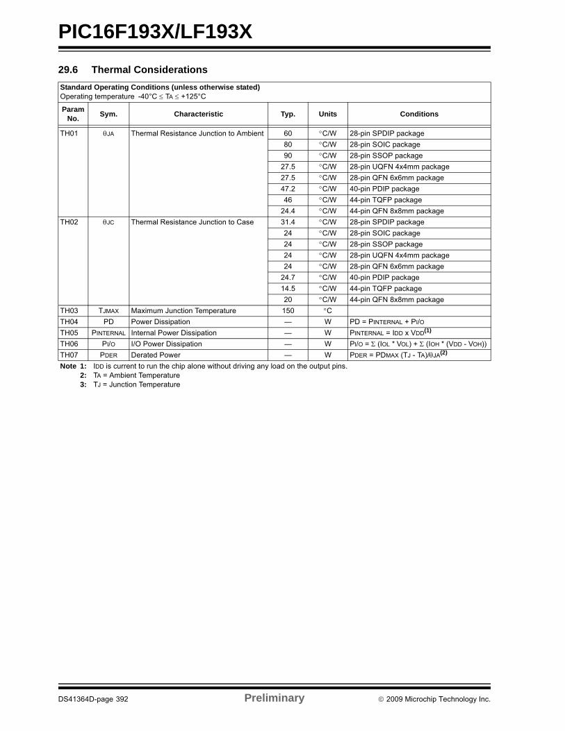
PIC16F193X/LF193X
29.6 Thermal Considerations
Standard Operating Conditions (unless otherwise stated)Operating temperature -40°C TA +125°C
ParamNo.
Sym. Characteristic Typ. Units Conditions
TH01 JA Thermal Resistance Junction to Ambient 60 C/W 28-pin SPDIP package
80 C/W 28-pin SOIC package
90 C/W 28-pin SSOP package
27.5 C/W 28-pin UQFN 4x4mm package
27.5 C/W 28-pin QFN 6x6mm package
47.2 C/W 40-pin PDIP package
46 C/W 44-pin TQFP package
24.4 C/W 44-pin QFN 8x8mm package
TH02 JC Thermal Resistance Junction to Case 31.4 C/W 28-pin SPDIP package
24 C/W 28-pin SOIC package
24 C/W 28-pin SSOP package
24 C/W 28-pin UQFN 4x4mm package
24 C/W 28-pin QFN 6x6mm package
24.7 C/W 40-pin PDIP package
14.5 C/W 44-pin TQFP package
20 C/W 44-pin QFN 8x8mm package
TH03 TJMAX Maximum Junction Temperature 150 CTH04 PD Power Dissipation — W PD = PINTERNAL + PI/O
TH05 PINTERNAL Internal Power Dissipation — W PINTERNAL = IDD x VDD(1)
TH06 PI/O I/O Power Dissipation — W PI/O = (IOL * VOL) + (IOH * (VDD - VOH))
TH07 PDER Derated Power — W PDER = PDMAX (TJ - TA)/JA(2)
Note 1: IDD is current to run the chip alone without driving any load on the output pins.2: TA = Ambient Temperature3: TJ = Junction Temperature
DS41364D-page 392 Preliminary 2009 Microchip Technology Inc.

PIC16F193X/LF193X
29.7 Timing Parameter Symbology
The timing parameter symbols have been created withone of the following formats:
FIGURE 29-5: LOAD CONDITIONS
1. TppS2ppS
2. TppS
T
F Frequency T Time
Lowercase letters (pp) and their meanings:
pp
cc CCP1 osc OSC1
ck CLKOUT rd RD
cs CS rw RD or WR
di SDI sc SCK
do SDO ss SS
dt Data in t0 T0CKI
io I/O PORT t1 T1CKI
mc MCLR wr WR
Uppercase letters and their meanings:
S
F Fall P Period
H High R Rise
I Invalid (High-impedance) V Valid
L Low Z High-impedance
VSS
CL
Legend: CL = 50 pF for all pins, 15 pF for OSC2 output
Load Condition
Pin
2009 Microchip Technology Inc. Preliminary DS41364D-page 393
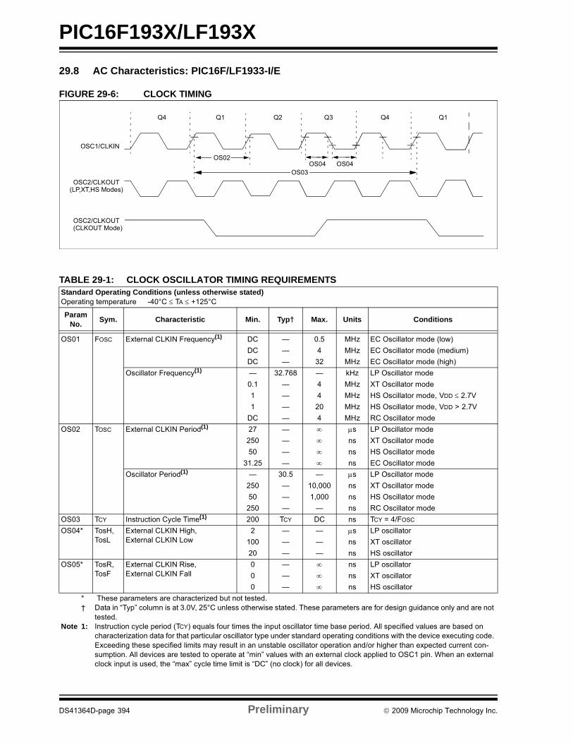
PIC16F193X/LF193X
29.8 AC Characteristics: PIC16F/LF1933-I/E
FIGURE 29-6: CLOCK TIMING
TABLE 29-1: CLOCK OSCILLATOR TIMING REQUIREMENTS
OSC1/CLKIN
OSC2/CLKOUT
Q4 Q1 Q2 Q3 Q4 Q1
OS02
OS03OS04 OS04
OSC2/CLKOUT(LP,XT,HS Modes)
(CLKOUT Mode)
Standard Operating Conditions (unless otherwise stated)Operating temperature -40°C TA +125°C
ParamNo.
Sym. Characteristic Min. Typ† Max. Units Conditions
OS01 FOSC External CLKIN Frequency(1) DC — 0.5 MHz EC Oscillator mode (low)
DC — 4 MHz EC Oscillator mode (medium)
DC — 32 MHz EC Oscillator mode (high)
Oscillator Frequency(1) — 32.768 — kHz LP Oscillator mode
0.1 — 4 MHz XT Oscillator mode
1 — 4 MHz HS Oscillator mode, VDD 2.7V
1 — 20 MHz HS Oscillator mode, VDD > 2.7V
DC — 4 MHz RC Oscillator mode
OS02 TOSC External CLKIN Period(1) 27 — s LP Oscillator mode
250 — ns XT Oscillator mode
50 — ns HS Oscillator mode
31.25 — ns EC Oscillator mode
Oscillator Period(1) — 30.5 — s LP Oscillator mode
250 — 10,000 ns XT Oscillator mode
50 — 1,000 ns HS Oscillator mode
250 — — ns RC Oscillator mode
OS03 TCY Instruction Cycle Time(1) 200 TCY DC ns TCY = 4/FOSC
OS04* TosH,TosL
External CLKIN High,External CLKIN Low
2 — — s LP oscillator
100 — — ns XT oscillator
20 — — ns HS oscillator
OS05* TosR,TosF
External CLKIN Rise,External CLKIN Fall
0 — ns LP oscillator
0 — ns XT oscillator
0 — ns HS oscillator
* These parameters are characterized but not tested.† Data in “Typ” column is at 3.0V, 25°C unless otherwise stated. These parameters are for design guidance only and are not
tested.Note 1: Instruction cycle period (TCY) equals four times the input oscillator time base period. All specified values are based on
characterization data for that particular oscillator type under standard operating conditions with the device executing code. Exceeding these specified limits may result in an unstable oscillator operation and/or higher than expected current con-sumption. All devices are tested to operate at “min” values with an external clock applied to OSC1 pin. When an external clock input is used, the “max” cycle time limit is “DC” (no clock) for all devices.
DS41364D-page 394 Preliminary 2009 Microchip Technology Inc.

PIC16F193X/LF193X
TABLE 29-2: OSCILLATOR PARAMETERS
TABLE 29-3: PLL CLOCK TIMING SPECIFICATIONS (VDD = 2.7V TO 5.5V)
Standard Operating Conditions (unless otherwise stated)Operating Temperature -40°C TA +125°C
Param No.
Sym. CharacteristicFreq.
ToleranceMin. Typ† Max. Units Conditions
OS08 HFOSC Internal Calibrated HFINTOSC Frequency(2)
2%2.5%
——
16.016.0
——
MHzMHz
0°C TA +60°C, VDD 2.5V60°C TA 85°C, VDD 2.5V
5% — 16.0 — MHz -40°C TA +125°C
OS08A MFOSC Internal Calibrated MFINTOSC Frequency(2)
2%2.5%
——
500500
——
kHzkHz
0°C TA +60°C, VDD 2.5V60°C TA 85°C, VDD 2.5V
5% — 500 — kHz -40°C TA +125°C
OS10* TIOSC ST HFINTOSCWake-up from Sleep Start-up TimeMFINTOSCWake-up from Sleep Start-up Time
— — 5 8 s
— — 20 30 s
* These parameters are characterized but not tested.† Data in “Typ” column is at 3.0V, 25°C unless otherwise stated. These parameters are for design guidance only and are not
tested.Note 1: Instruction cycle period (TCY) equals four times the input oscillator time base period. All specified values are based on
characterization data for that particular oscillator type under standard operating conditions with the device executing code. Exceeding these specified limits may result in an unstable oscillator operation and/or higher than expected current con-sumption. All devices are tested to operate at “min” values with an external clock applied to the OSC1 pin. When an exter-nal clock input is used, the “max” cycle time limit is “DC” (no clock) for all devices.
2: To ensure these oscillator frequency tolerances, VDD and VSS must be capacitively decoupled as close to the device as possible. 0.1 F and 0.01 F values in parallel are recommended.
3: By design.
Param No.
Sym. Characteristic Min. Typ† Max. Units Conditions
F10 FOSC Oscillator Frequency Range 4 — 8 MHz
F11 FSYS On-Chip VCO System Frequency 16 — 32 MHz
F12 TRC PLL Start-up Time (Lock Time) — — 2 ms
F13* CLK CLKOUT Stability (Jitter) -0.25% — +0.25% %
* These parameters are characterized but not tested.
† Data in “Typ” column is at 5V, 25C unless otherwise stated. These parameters are for design guidance only and are not tested.
2009 Microchip Technology Inc. Preliminary DS41364D-page 395
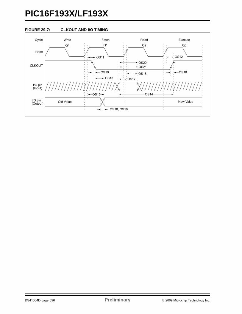
PIC16F193X/LF193X
FIGURE 29-7: CLKOUT AND I/O TIMING
FOSC
CLKOUT
I/O pin(Input)
I/O pin(Output)
Q4 Q1 Q2 Q3
OS11
OS19
OS13
OS15
OS18, OS19
OS20OS21
OS17
OS16
OS14
OS12
OS18
Old Value New Value
Write Fetch Read ExecuteCycle
DS41364D-page 396 Preliminary 2009 Microchip Technology Inc.
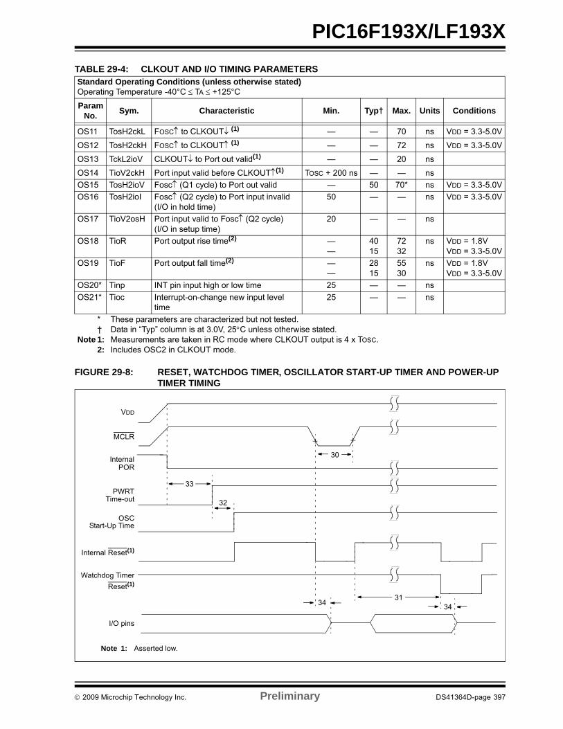
PIC16F193X/LF193X
TABLE 29-4: CLKOUT AND I/O TIMING PARAMETERS
FIGURE 29-8: RESET, WATCHDOG TIMER, OSCILLATOR START-UP TIMER AND POWER-UP TIMER TIMING
Standard Operating Conditions (unless otherwise stated)Operating Temperature -40°C TA +125°C
Param No.
Sym. Characteristic Min. Typ† Max. Units Conditions
OS11 TosH2ckL FOSC to CLKOUT (1) — — 70 ns VDD = 3.3-5.0V
OS12 TosH2ckH FOSC to CLKOUT (1) — — 72 ns VDD = 3.3-5.0V
OS13 TckL2ioV CLKOUT to Port out valid(1) — — 20 ns
OS14 TioV2ckH Port input valid before CLKOUT(1) TOSC + 200 ns — — ns
OS15 TosH2ioV Fosc (Q1 cycle) to Port out valid — 50 70* ns VDD = 3.3-5.0V
OS16 TosH2ioI Fosc (Q2 cycle) to Port input invalid (I/O in hold time)
50 — — ns VDD = 3.3-5.0V
OS17 TioV2osH Port input valid to Fosc(Q2 cycle)(I/O in setup time)
20 — — ns
OS18 TioR Port output rise time(2) ——
4015
7232
ns VDD = 1.8VVDD = 3.3-5.0V
OS19 TioF Port output fall time(2) ——
2815
5530
ns VDD = 1.8VVDD = 3.3-5.0V
OS20* Tinp INT pin input high or low time 25 — — ns
OS21* Tioc Interrupt-on-change new input level time
25 — — ns
* These parameters are characterized but not tested.† Data in “Typ” column is at 3.0V, 25C unless otherwise stated.
Note 1: Measurements are taken in RC mode where CLKOUT output is 4 x TOSC.2: Includes OSC2 in CLKOUT mode.
VDD
MCLR
InternalPOR
PWRTTime-out
OSCStart-Up Time
Internal Reset(1)
Watchdog Timer
33
32
30
3134
I/O pins
34
Note 1: Asserted low.
Reset(1)
2009 Microchip Technology Inc. Preliminary DS41364D-page 397

PIC16F193X/LF193X
FIGURE 29-9: BROWN-OUT RESET TIMING AND CHARACTERISTICS
VBOR
VDD
(Device in Brown-out Reset) (Device not in Brown-out Reset)
33(1)
Note 1: 64 ms delay only if PWRTE bit in the Configuration Word register is programmed to ‘0’. 2 ms delay if PWRTE = 0 and VREGEN = 1.
Reset
(due to BOR)
VBOR and VHYST
37
DS41364D-page 398 Preliminary 2009 Microchip Technology Inc.

PIC16F193X/LF193X
TABLE 29-5: RESET, WATCHDOG TIMER, OSCILLATOR START-UP TIMER, POWER-UP TIMER AND BROWN-OUT RESET PARAMETERS
FIGURE 29-10: TIMER0 AND TIMER1 EXTERNAL CLOCK TIMINGS
Standard Operating Conditions (unless otherwise stated)Operating Temperature -40°C TA +125°C
Param No.
Sym. Characteristic Min. Typ† Max. Units Conditions
30 TMCL MCLR Pulse Width (low) 2 5
——
——
ss
VDD = 3.3-5V, -40°C to +85°CVDD = 3.3-5V
31 TWDTLP Low-Power Watchdog Timer Time-out Period (No Prescaler)
10 18 27 ms VDD = 3.3V-5V
32 TOST Oscillator Start-up Timer Period(1), (2) — 1024 — Tosc (Note 3)
33* TPWRT Power-up Timer Period, PWRTE = 0 40 65 140 ms
34* TIOZ I/O high-impedance from MCLR Low or Watchdog Timer Reset
— — 2.0 s
35 VBOR Brown-out Reset Voltage 2.381.80
2.51.9
2.732.11
V BORV=2.5VBORV=1.9V
36* VHYST Brown-out Reset Hysteresis 0 25 50 mV -40°C to +85°C
37* TBORDC Brown-out Reset DC Response Time
1 3 5 s VDD VBOR
* These parameters are characterized but not tested.† Data in “Typ” column is at 3.0V, 25°C unless otherwise stated. These parameters are for design guidance
only and are not tested.Note 1: Instruction cycle period (TCY) equals four times the input oscillator time base period. All specified values are
based on characterization data for that particular oscillator type under standard operating conditions with the device executing code. Exceeding these specified limits may result in an unstable oscillator operation and/or higher than expected current consumption. All devices are tested to operate at “min” values with an external clock applied to the OSC1 pin. When an external clock input is used, the “max” cycle time limit is “DC” (no clock) for all devices.
2: By design.3: Period of the slower clock.4: To ensure these voltage tolerances, VDD and VSS must be capacitively decoupled as close to the device as
possible. 0.1 F and 0.01 F values in parallel are recommended.
T0CKI
T1CKI
40 41
42
45 46
47 49
TMR0 orTMR1
2009 Microchip Technology Inc. Preliminary DS41364D-page 399

PIC16F193X/LF193X
TABLE 29-6: TIMER0 AND TIMER1 EXTERNAL CLOCK REQUIREMENTS
FIGURE 29-11: CAPTURE/COMPARE/PWM TIMINGS (CCP)
TABLE 29-7: CAPTURE/COMPARE/PWM REQUIREMENTS (CCP)
Standard Operating Conditions (unless otherwise stated)Operating Temperature -40°C TA +125°C
Param No.
Sym. Characteristic Min. Typ† Max. Units Conditions
40* TT0H T0CKI High Pulse Width No Prescaler 0.5 TCY + 20 — — ns
With Prescaler 10 — — ns
41* TT0L T0CKI Low Pulse Width No Prescaler 0.5 TCY + 20 — — ns
With Prescaler 10 — — ns
42* TT0P T0CKI Period Greater of:20 or TCY + 40
N
— — ns N = prescale value (2, 4, ..., 256)
45* TT1H T1CKI High Time
Synchronous, No Prescaler 0.5 TCY + 20 — — ns
Synchronous, with Prescaler
15 — — ns
Asynchronous 30 — — ns
46* TT1L T1CKI Low Time
Synchronous, No Prescaler 0.5 TCY + 20 — — ns
Synchronous, with Prescaler 15 — — ns
Asynchronous 30 — — ns
47* TT1P T1CKI Input Period
Synchronous Greater of:30 or TCY + 40
N
— — ns N = prescale value (1, 2, 4, 8)
Asynchronous 60 — — ns
48 FT1 Timer1 Oscillator Input Frequency Range (oscillator enabled by setting bit T1OSCEN)
32.4 32.768 33.1 kHz
49* TCKEZTMR1 Delay from External Clock Edge to Timer Increment
2 TOSC — 7 TOSC — Timers in Sync mode
* These parameters are characterized but not tested.† Data in “Typ” column is at 3.0V, 25°C unless otherwise stated. These parameters are for design guidance only and are not
tested.
Standard Operating Conditions (unless otherwise stated)Operating Temperature -40°C TA +125°C
Param No.
Sym. Characteristic Min. Typ† Max. Units Conditions
CC01* TccL CCPx Input Low Time No Prescaler 0.5TCY + 20 — — ns
With Prescaler 20 — — ns
CC02* TccH CCPx Input High Time No Prescaler 0.5TCY + 20 — — ns
With Prescaler 20 — — ns
CC03* TccP CCPx Input Period 3TCY + 40N
— — ns N = prescale value (1, 4 or 16)
* These parameters are characterized but not tested.† Data in “Typ” column is at 3.0V, 25°C unless otherwise stated. These parameters are for design guidance only and are not
tested.
Note: Refer to Figure 29.5 for load conditions.
(Capture mode)
CC01 CC02
CC03
CCPx
DS41364D-page 400 Preliminary 2009 Microchip Technology Inc.

PIC16F193X/LF193X
TABLE 29-8: PIC16F/LF1933 A/D CONVERTER (ADC) CHARACTERISTICS:
TABLE 29-9: PIC16F/LF1933 A/D CONVERSION REQUIREMENTS
Standard Operating Conditions (unless otherwise stated)Operating temperature -40°C TA +125°C
Param No.
Sym. Characteristic Min. Typ† Max. Units Conditions
AD01 NR Resolution — — 10 bit
AD02 EIL Integral Error — — ±1.7 LSb VREF = 3.0V
AD03 EDL Differential Error — — ±1 LSb No missing codesVREF = 3.0V
AD04 EOFF Offset Error — — ±2.5 LSb VREF = 3.0V
AD05 EGN Gain Error — — ±2.0 LSb VREF = 3.0V
AD06 VREF Reference Voltage(3) 1.8 — VDD V = (VREF+ minus VREF-)
AD07 VAIN Full-Scale Range VSS — VREF V
AD08 ZAIN Recommended Impedance of Analog Voltage Source
— — 50 k Can go higher if external 0.01F capacitor is present on input pin.
* These parameters are characterized but not tested.† Data in “Typ” column is at 3.0V, 25°C unless otherwise stated. These parameters are for design guidance only and are not
tested.Note 1: Total Absolute Error includes integral, differential, offset and gain errors.
2: The A/D conversion result never decreases with an increase in the input voltage and has no missing codes.3: ADC VREF is from external VREF, VDD pin or FVREF, whichever is selected as reference input.4: When ADC is off, it will not consume any current other than leakage current. The power-down current specification
includes any such leakage from the ADC module.
Standard Operating Conditions (unless otherwise stated)Operating temperature -40°C TA +125°C
ParamNo.
Sym. Characteristic Min. Typ† Max. Units Conditions
AD130* TAD A/D Clock Period 1.0 — 9.0 s TOSC-based
A/D Internal RC Oscillator Period
1.0 1.6 6.0 s ADCS<1:0> = 11 (ADRC mode)
AD131 TCNV Conversion Time (not including Acquisition Time)(1)
— 11 — TAD Set GO/DONE bit to conversioncomplete
AD132* TACQ Acquisition Time — 5.0 — s
* These parameters are characterized but not tested.† Data in “Typ” column is at 3.0V, 25°C unless otherwise stated. These parameters are for design guidance only and are not
tested.Note 1: The ADRES register may be read on the following TCY cycle.
2009 Microchip Technology Inc. Preliminary DS41364D-page 401
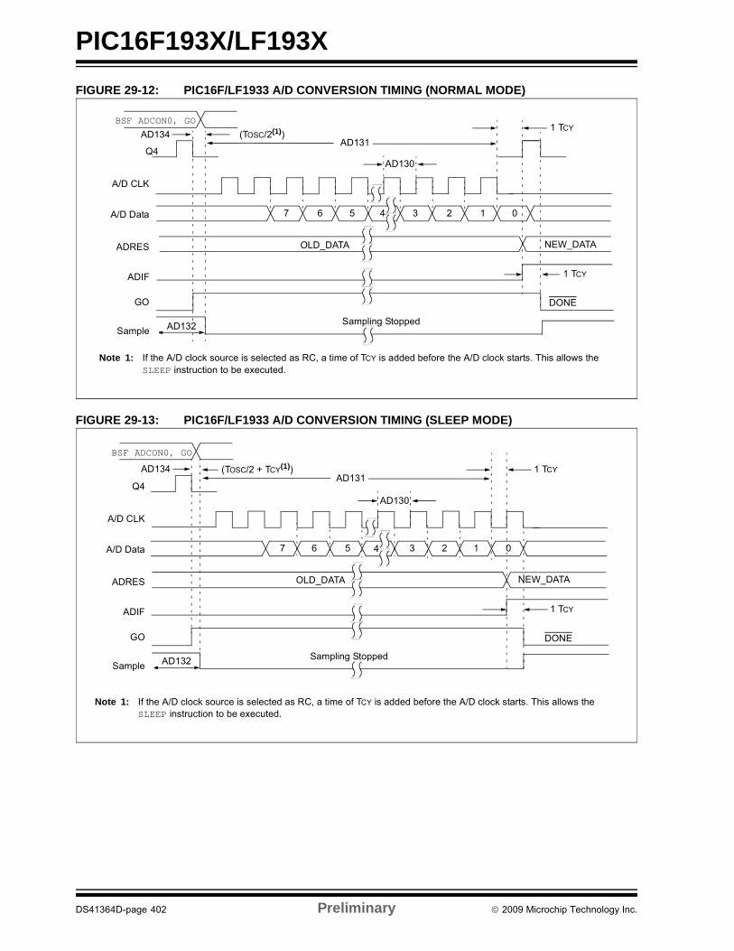
PIC16F193X/LF193X
FIGURE 29-12: PIC16F/LF1933 A/D CONVERSION TIMING (NORMAL MODE)
FIGURE 29-13: PIC16F/LF1933 A/D CONVERSION TIMING (SLEEP MODE)
AD131
AD130
BSF ADCON0, GO
Q4
A/D CLK
A/D Data
ADRES
ADIF
GO
Sample
OLD_DATA
Sampling Stopped
DONE
NEW_DATA
7 6 5 3 2 1 0
Note 1: If the A/D clock source is selected as RC, a time of TCY is added before the A/D clock starts. This allows the SLEEP instruction to be executed.
1 TCY
4
AD134 (TOSC/2(1))
1 TCY
AD132
AD132
AD131
AD130
BSF ADCON0, GO
Q4
A/D CLK
A/D Data
ADRES
ADIF
GO
Sample
OLD_DATA
Sampling Stopped
DONE
NEW_DATA
7 5 3 2 1 0
Note 1: If the A/D clock source is selected as RC, a time of TCY is added before the A/D clock starts. This allows the SLEEP instruction to be executed.
AD134
46
1 TCY(TOSC/2 + TCY(1))
1 TCY
DS41364D-page 402 Preliminary 2009 Microchip Technology Inc.

PIC16F193X/LF193X
TABLE 29-10: COMPARATOR SPECIFICATIONS
TABLE 29-11: DIGITAL-TO-ANALOG CONVERTER (DAC) SPECIFICATIONS
FIGURE 29-14: USART SYNCHRONOUS TRANSMISSION (MASTER/SLAVE) TIMING
Operating Conditions: 1.8V < VDD < 5.5V, -40°C < TA < +125°C (unless otherwise stated).
ParamNo.
Sym. Characteristics Min. Typ. Max. Units Comments
CM01 VIOFF Input Offset Voltage — ±7.5 ±60 mV
CM02 VICM Input Common Mode Voltage 0 — VDD V
CM03 CMRR Common Mode Rejection Ratio — 50 — dB
CM04 TRESP Response Time — 150 400 ns Note 1
CM05 TMC2OV Comparator Mode Change to Output Valid*
— — 10 s
CM06 CHYSTER Comparator Hysteresis — 65 — mV
* These parameters are characterized but not tested.
Note 1: Response time measured with one comparator input at VDD/2, while the other input transitions from VSS to VDD.
Operating Conditions: 1.8V < VDD < 5.5V, -40°C < TA < +125°C (unless otherwise stated).
ParamNo.
Sym. Characteristics Min. Typ. Max. Units Comments
DAC01* CLSB Step Size(2) — VDD/32 — V
DAC02* CACC Absolute Accuracy — — 1/2 LSb
DAC03* CR Unit Resistor Value (R) — TBD —
DAC04* CST Settling Time(1) — — 10 s
* These parameters are characterized but not tested.Legend: TBD = To Be Determined
Note 1: Settling time measured while DACR<4:0> transitions from ‘0000’ to ‘1111’.
Note: Refer to Figure 29-5 for load conditions.
US121 US121
US120 US122
CK
DT
2009 Microchip Technology Inc. Preliminary DS41364D-page 403
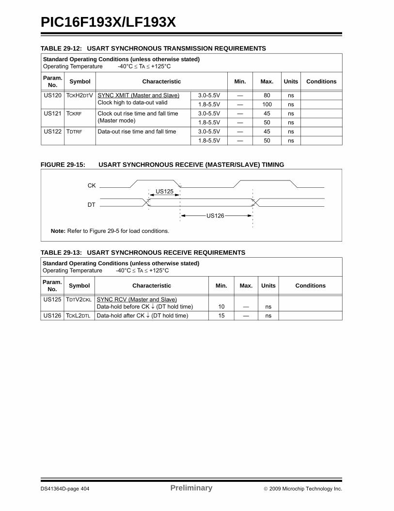
PIC16F193X/LF193X
TABLE 29-12: USART SYNCHRONOUS TRANSMISSION REQUIREMENTS
FIGURE 29-15: USART SYNCHRONOUS RECEIVE (MASTER/SLAVE) TIMING
TABLE 29-13: USART SYNCHRONOUS RECEIVE REQUIREMENTS
Standard Operating Conditions (unless otherwise stated)Operating Temperature -40°C TA +125°C
Param. No.
Symbol Characteristic Min. Max. Units Conditions
US120 TCKH2DTV SYNC XMIT (Master and Slave)Clock high to data-out valid
3.0-5.5V — 80 ns
1.8-5.5V — 100 ns
US121 TCKRF Clock out rise time and fall time (Master mode)
3.0-5.5V — 45 ns
1.8-5.5V — 50 ns
US122 TDTRF Data-out rise time and fall time 3.0-5.5V — 45 ns
1.8-5.5V — 50 ns
Standard Operating Conditions (unless otherwise stated)Operating Temperature -40°C TA +125°C
Param. No.
Symbol Characteristic Min. Max. Units Conditions
US125 TDTV2CKL SYNC RCV (Master and Slave)Data-hold before CK (DT hold time) 10 — ns
US126 TCKL2DTL Data-hold after CK (DT hold time) 15 — ns
Note: Refer to Figure 29-5 for load conditions.
US125
US126
CK
DT
DS41364D-page 404 Preliminary 2009 Microchip Technology Inc.

PIC16F193X/LF193X
FIGURE 29-16: SPI MASTER MODE TIMING (CKE = 0, SMP = 0)
FIGURE 29-17: SPI MASTER MODE TIMING (CKE = 1, SMP = 1)
SS
SCK(CKP = 0)
SCK(CKP = 1)
SDO
SDI
SP70
SP71 SP72
SP73SP74
SP75, SP76
SP78SP79
SP80
SP79SP78
MSb LSbbit 6 - - - - - -1
MSb In LSb Inbit 6 - - - -1
Note: Refer to Figure 29-5 for load conditions.
SS
SCK(CKP = 0)
SCK(CKP = 1)
SDO
SDI
SP81
SP71 SP72
SP74
SP75, SP76
SP78SP80
MSb
SP79SP73
MSb In
bit 6 - - - - - -1
LSb Inbit 6 - - - -1
LSb
Note: Refer to Figure 29-5 for load conditions.
2009 Microchip Technology Inc. Preliminary DS41364D-page 405

PIC16F193X/LF193X
FIGURE 29-18: SPI SLAVE MODE TIMING (CKE = 0)
FIGURE 29-19: SPI SLAVE MODE TIMING (CKE = 1)
SS
SCK(CKP = 0)
SCK(CKP = 1)
SDO
SDI
SP70
SP71 SP72
SP73
SP74
SP75, SP76 SP77
SP78SP79
SP80
SP79SP78
MSb LSbbit 6 - - - - - -1
MSb In bit 6 - - - -1 LSb In
SP83
Note: Refer to Figure 29-5 for load conditions.
SS
SCK(CKP = 0)
SCK(CKP = 1)
SDO
SDI
SP70
SP71 SP72
SP82
SP74
SP75, SP76
MSb bit 6 - - - - - -1 LSb
SP77
MSb In bit 6 - - - -1 LSb In
SP80
SP83
Note: Refer to Figure 29-5 for load conditions.
DS41364D-page 406 Preliminary 2009 Microchip Technology Inc.
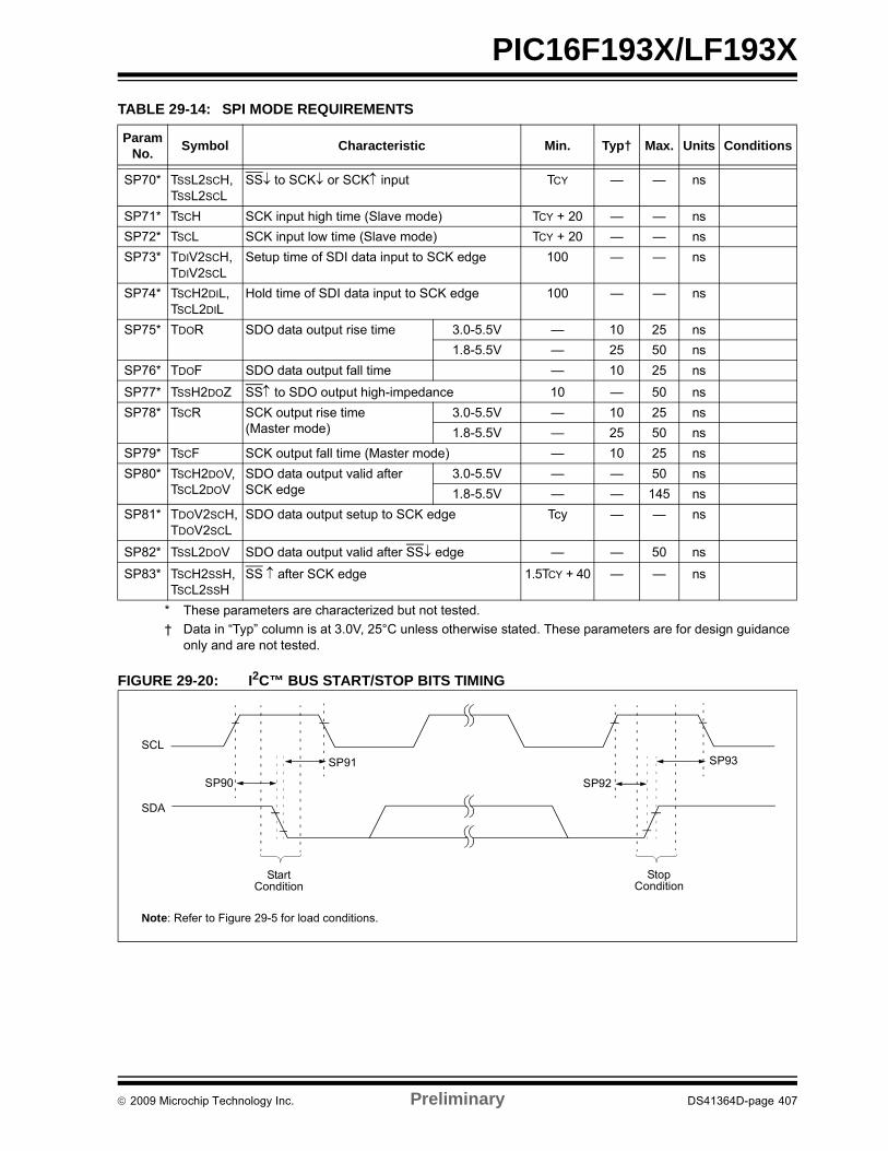
PIC16F193X/LF193X
TABLE 29-14: SPI MODE REQUIREMENTS
FIGURE 29-20: I2C™ BUS START/STOP BITS TIMING
Param No.
Symbol Characteristic Min. Typ† Max. Units Conditions
SP70* TSSL2SCH, TSSL2SCL
SS to SCK or SCK input TCY — — ns
SP71* TSCH SCK input high time (Slave mode) TCY + 20 — — ns
SP72* TSCL SCK input low time (Slave mode) TCY + 20 — — ns
SP73* TDIV2SCH, TDIV2SCL
Setup time of SDI data input to SCK edge 100 — — ns
SP74* TSCH2DIL, TSCL2DIL
Hold time of SDI data input to SCK edge 100 — — ns
SP75* TDOR SDO data output rise time 3.0-5.5V — 10 25 ns
1.8-5.5V — 25 50 ns
SP76* TDOF SDO data output fall time — 10 25 ns
SP77* TSSH2DOZ SS to SDO output high-impedance 10 — 50 ns
SP78* TSCR SCK output rise time (Master mode)
3.0-5.5V — 10 25 ns
1.8-5.5V — 25 50 ns
SP79* TSCF SCK output fall time (Master mode) — 10 25 ns
SP80* TSCH2DOV,TSCL2DOV
SDO data output valid after SCK edge
3.0-5.5V — — 50 ns
1.8-5.5V — — 145 ns
SP81* TDOV2SCH,TDOV2SCL
SDO data output setup to SCK edge Tcy — — ns
SP82* TSSL2DOV SDO data output valid after SS edge — — 50 ns
SP83* TSCH2SSH,TSCL2SSH
SS after SCK edge 1.5TCY + 40 — — ns
* These parameters are characterized but not tested.
† Data in “Typ” column is at 3.0V, 25°C unless otherwise stated. These parameters are for design guidance only and are not tested.
Note: Refer to Figure 29-5 for load conditions.
SP91
SP92
SP93SCL
SDA
StartCondition
StopCondition
SP90
2009 Microchip Technology Inc. Preliminary DS41364D-page 407
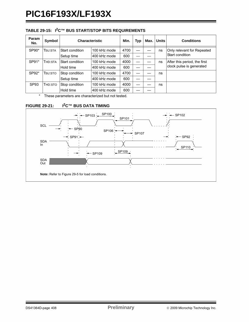
PIC16F193X/LF193X
TABLE 29-15: I2C™ BUS START/STOP BITS REQUIREMENTS
FIGURE 29-21: I2C™ BUS DATA TIMING
ParamNo.
Symbol Characteristic Min. Typ Max. Units Conditions
SP90* TSU:STA Start condition 100 kHz mode 4700 — — ns Only relevant for Repeated Start conditionSetup time 400 kHz mode 600 — —
SP91* THD:STA Start condition 100 kHz mode 4000 — — ns After this period, the first clock pulse is generatedHold time 400 kHz mode 600 — —
SP92* TSU:STO Stop condition 100 kHz mode 4700 — — ns
Setup time 400 kHz mode 600 — —
SP93 THD:STO Stop condition 100 kHz mode 4000 — — ns
Hold time 400 kHz mode 600 — —
* These parameters are characterized but not tested.
Note: Refer to Figure 29-5 for load conditions.
SP90
SP91 SP92
SP100SP101
SP103
SP106SP107
SP109SP109
SP110
SP102
SCL
SDAIn
SDAOut
DS41364D-page 408 Preliminary 2009 Microchip Technology Inc.
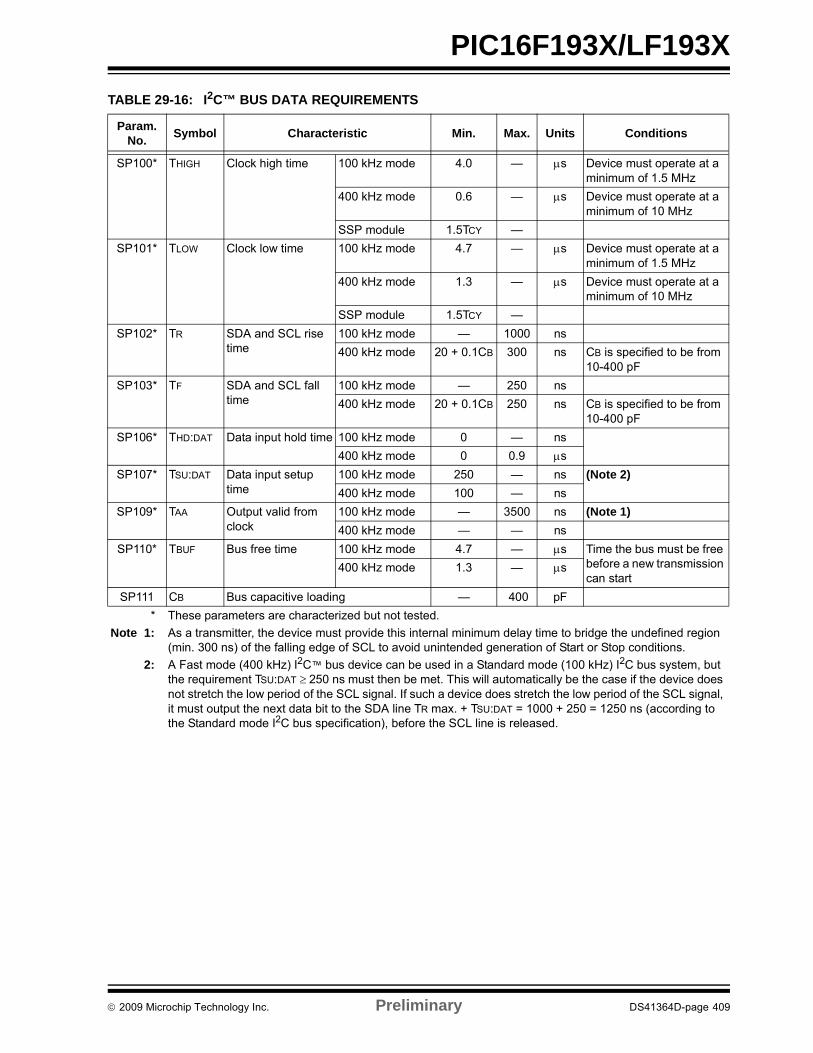
PIC16F193X/LF193X
TABLE 29-16: I2C™ BUS DATA REQUIREMENTS
Param.No.
Symbol Characteristic Min. Max. Units Conditions
SP100* THIGH Clock high time 100 kHz mode 4.0 — s Device must operate at a minimum of 1.5 MHz
400 kHz mode 0.6 — s Device must operate at a minimum of 10 MHz
SSP module 1.5TCY —
SP101* TLOW Clock low time 100 kHz mode 4.7 — s Device must operate at a minimum of 1.5 MHz
400 kHz mode 1.3 — s Device must operate at a minimum of 10 MHz
SSP module 1.5TCY —
SP102* TR SDA and SCL rise time
100 kHz mode — 1000 ns
400 kHz mode 20 + 0.1CB 300 ns CB is specified to be from 10-400 pF
SP103* TF SDA and SCL fall time
100 kHz mode — 250 ns
400 kHz mode 20 + 0.1CB 250 ns CB is specified to be from 10-400 pF
SP106* THD:DAT Data input hold time 100 kHz mode 0 — ns
400 kHz mode 0 0.9 s
SP107* TSU:DAT Data input setup time
100 kHz mode 250 — ns (Note 2)
400 kHz mode 100 — ns
SP109* TAA Output valid from clock
100 kHz mode — 3500 ns (Note 1)
400 kHz mode — — ns
SP110* TBUF Bus free time 100 kHz mode 4.7 — s Time the bus must be free before a new transmission can start
400 kHz mode 1.3 — s
SP111 CB Bus capacitive loading — 400 pF
* These parameters are characterized but not tested.
Note 1: As a transmitter, the device must provide this internal minimum delay time to bridge the undefined region (min. 300 ns) of the falling edge of SCL to avoid unintended generation of Start or Stop conditions.
2: A Fast mode (400 kHz) I2C™ bus device can be used in a Standard mode (100 kHz) I2C bus system, but the requirement TSU:DAT 250 ns must then be met. This will automatically be the case if the device does not stretch the low period of the SCL signal. If such a device does stretch the low period of the SCL signal, it must output the next data bit to the SDA line TR max. + TSU:DAT = 1000 + 250 = 1250 ns (according to the Standard mode I2C bus specification), before the SCL line is released.
2009 Microchip Technology Inc. Preliminary DS41364D-page 409
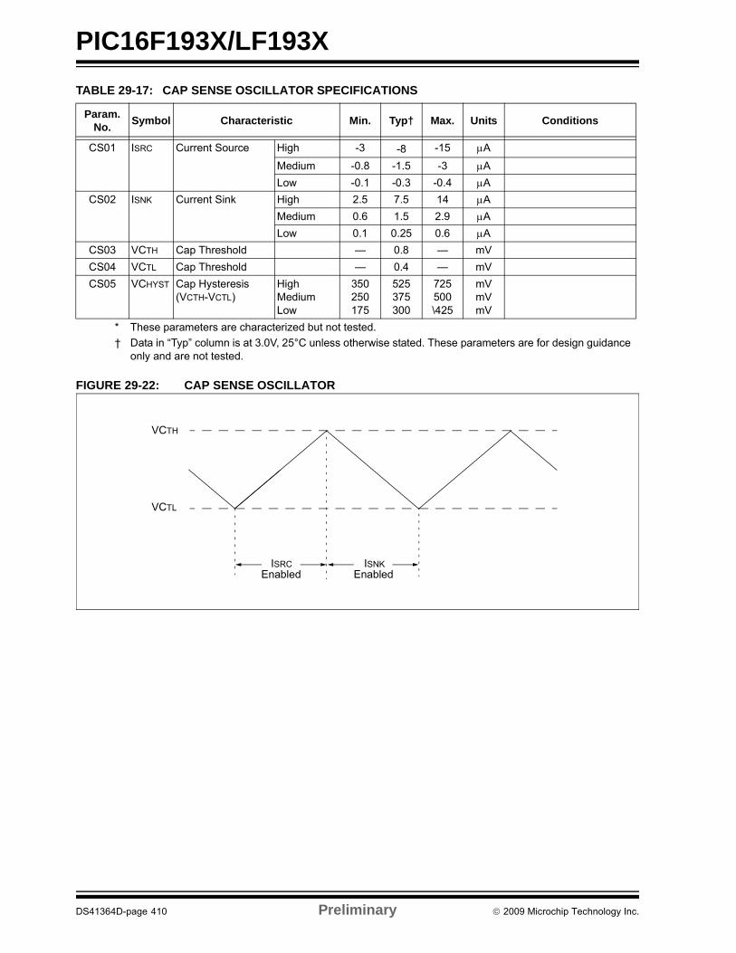
PIC16F193X/LF193X
TABLE 29-17: CAP SENSE OSCILLATOR SPECIFICATIONS
FIGURE 29-22: CAP SENSE OSCILLATOR
Param.No.
Symbol Characteristic Min. Typ† Max. Units Conditions
CS01 ISRC Current Source High -3 -8 -15 A
Medium -0.8 -1.5 -3 A
Low -0.1 -0.3 -0.4 A
CS02 ISNK Current Sink High 2.5 7.5 14 A
Medium 0.6 1.5 2.9 A
Low 0.1 0.25 0.6 A
CS03 VCTH Cap Threshold — 0.8 — mV
CS04 VCTL Cap Threshold — 0.4 — mV
CS05 VCHYST Cap Hysteresis (VCTH-VCTL)
HighMediumLow
350250175
525375300
725500\425
mVmVmV
* These parameters are characterized but not tested.
† Data in “Typ” column is at 3.0V, 25°C unless otherwise stated. These parameters are for design guidance only and are not tested.
ISRC
VCTH
VCTL
ISNKEnabledEnabled
DS41364D-page 410 Preliminary 2009 Microchip Technology Inc.

PIC16F193X/LF193X
30.0 ELECTRICAL SPECIFICATIONS (PIC16F/LF1934/36/37)
Absolute Maximum Ratings(†)
Ambient temperature under bias....................................................................................................... -40°C to +125°C
Storage temperature ........................................................................................................................ -65°C to +150°C
Voltage on VDD with respect to VSS, PIC16F1934/36/37 ................................................................... -0.3V to +6.5V
Voltage on VCAP pin with respect to VSS, PIC16F1934/36/37 ............................................................. -0.3V to +4.0V
Voltage on VDD with respect to VSS, PIC16LF1934/36/37 ................................................................. -0.3V to +4.0V
Voltage on MCLR with respect to Vss ................................................................................................. -0.3V to +9.0V
Voltage on all other pins with respect to VSS ........................................................................... -0.3V to (VDD + 0.3V)
Total power dissipation(1) ............................................................................................................................... 800 mW
Maximum current out of VSS(2) pin, -40°C TA +85°C for industrial ........................................................... 255 mA
Maximum current out of VSS(2) pin, -40°C TA +125°C for extended........................................................ 105 mA
Maximum current into VDD(2) pin, -40°C TA +85°C for industrial .............................................................. 170 mA
Maximum current into VDD(2) pin, -40°C TA +125°C for extended............................................................. 70 mA
Maximum current out of VSS(3) pin, -40°C TA +85°C for industrial ............................................................ 340mA
Maximum current out of VSS(3) pin, -40°C TA +125°C for extended........................................................ 140 mA
Maximum current into VDD(3) pin, -40°C TA +85°C for industrial .............................................................. 255 mA
Maximum current into VDD(3) pin, -40°C TA +125°C for extended........................................................... 105 mA
Clamp current, IK (VPIN < 0 or VPIN > VDD)20 mA
Maximum output current sunk by any I/O pin.................................................................................................... 25 mA
Maximum output current sourced by any I/O pin .............................................................................................. 25 mA
Note 1: Power dissipation is calculated as follows: PDIS = VDD x {IDD – IOH} + {(VDD – VOH) x IOH} + (VOl x IOL)
2: For 28-pin devices.
3: For 40-pin devices..
† NOTICE: Stresses above those listed under “Absolute Maximum Ratings” may cause permanent damage to the device. This is a stress rating only and functional operation of the device at those or any other conditions above those indicated in the operation listings of this specification is not implied. Exposure above maximum rating conditions for extended periods may affect device reliability.
2009 Microchip Technology Inc. Preliminary DS41364D-page 411

PIC16F193X/LF193X
FIGURE 30-1: PIC16F/LF1934/36/37 VOLTAGE FREQUENCY GRAPH, -40°C TA +125°C
FIGURE 30-2: PIC16F/LF1934/36/37 VOLTAGE FREQUENCY GRAPH, -40°C TA +125°C
1.8
2.5
2.0
0
2.3
Frequency (MHz)
VD
D (
V)
Note 1: The shaded region indicates the permissible combinations of voltage and frequency.2: Refer to Table 30-1 for each Oscillator mode’s supported frequencies.
4 3210 16
5.5
3.6
1.8
2.5
2.0
0
2.3
Frequency (MHz)
VD
D (
V)
Note 1: The shaded region indicates the permissible combinations of voltage and frequency.2: Refer to Table 30-1 for each Oscillator mode’s supported frequencies.
4 3210 16
3.6
DS41364D-page 412 Preliminary 2009 Microchip Technology Inc.

PIC16F193X/LF193X
FIGURE 30-3: HFINTOSC FREQUENCY ACCURACY OVER DEVICE VDD AND TEMPERATURE
125
25
2.0
0
60
85
VDD (V)
4.0 5.04.5
Tem
pe
ratu
re (
°C)
2.5 3.0 3.5 5.51.8-40
-20
± 5%
± 2%
± 5%
± 2.5%
2009 Microchip Technology Inc. Preliminary DS41364D-page 413
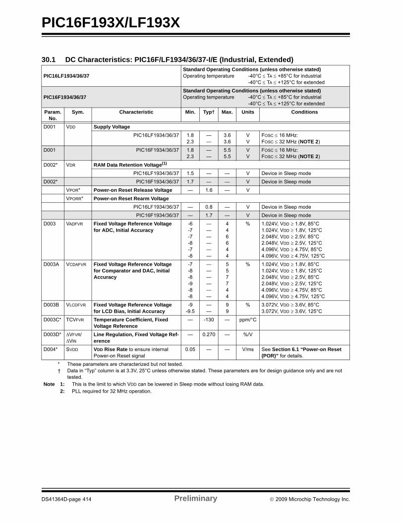
PIC16F193X/LF193X
30.1 DC Characteristics: PIC16F/LF1934/36/37-I/E (Industrial, Extended)
PIC16LF1934/36/37Standard Operating Conditions (unless otherwise stated)Operating temperature -40°C TA +85°C for industrial
-40°C TA +125°C for extended
PIC16F1934/36/37Standard Operating Conditions (unless otherwise stated)Operating temperature -40°C TA +85°C for industrial
-40°C TA +125°C for extended
Param. No.
Sym. Characteristic Min. Typ† Max. Units Conditions
D001 VDD Supply Voltage
PIC16LF1934/36/37 1.82.3
——
3.63.6
VV
FOSC 16 MHz:FOSC 32 MHz (NOTE 2)
D001 PIC16F1934/36/37 1.82.3
——
5.55.5
VV
FOSC 16 MHz:FOSC 32 MHz (NOTE 2)
D002* VDR RAM Data Retention Voltage(1)
PIC16LF1934/36/37 1.5 — — V Device in Sleep mode
D002* PIC16F1934/36/37 1.7 — — V Device in Sleep mode
VPOR* Power-on Reset Release Voltage — 1.6 — V
VPORR* Power-on Reset Rearm Voltage
PIC16LF1934/36/37 — 0.8 — V Device in Sleep mode
PIC16F1934/36/37 — 1.7 — V Device in Sleep mode
D003 VADFVR Fixed Voltage Reference Voltage for ADC, Initial Accuracy
-6-7-7-8-7-8
——————
446644
% 1.024V, VDD 1.8V, 85°C1.024V, VDD 1.8V, 125°C2.048V, VDD 2.5V, 85°C2.048V, VDD 2.5V, 125°C4.096V, VDD 4.75V, 85°C4.096V, VDD 4.75V, 125°C
D003A VCDAFVR Fixed Voltage Reference Voltage for Comparator and DAC, Initial Accuracy
-7-8-8-9-8-8
——————
557744
% 1.024V, VDD 1.8V, 85°C1.024V, VDD 1.8V, 125°C2.048V, VDD 2.5V, 85°C2.048V, VDD 2.5V, 125°C4.096V, VDD 4.75V, 85°C4.096V, VDD 4.75V, 125°C
D003B VLCDFVR Fixed Voltage Reference Voltage for LCD Bias, Initial Accuracy
-9-9.5
——
99
% 3.072V, VDD 3.6V, 85°C3.072V, VDD 3.6V, 125°C
D003C* TCVFVR Temperature Coefficient, Fixed Voltage Reference
— -130 — ppm/°C
D003D* VFVR/VIN
Line Regulation, Fixed Voltage Ref-erence
— 0.270 — %/V
D004* SVDD VDD Rise Rate to ensure internal Power-on Reset signal
0.05 — — V/ms See Section 6.1 “Power-on Reset (POR)” for details.
* These parameters are characterized but not tested.† Data in “Typ” column is at 3.3V, 25°C unless otherwise stated. These parameters are for design guidance only and are not
tested.
Note 1: This is the limit to which VDD can be lowered in Sleep mode without losing RAM data.2: PLL required for 32 MHz operation.
DS41364D-page 414 Preliminary 2009 Microchip Technology Inc.
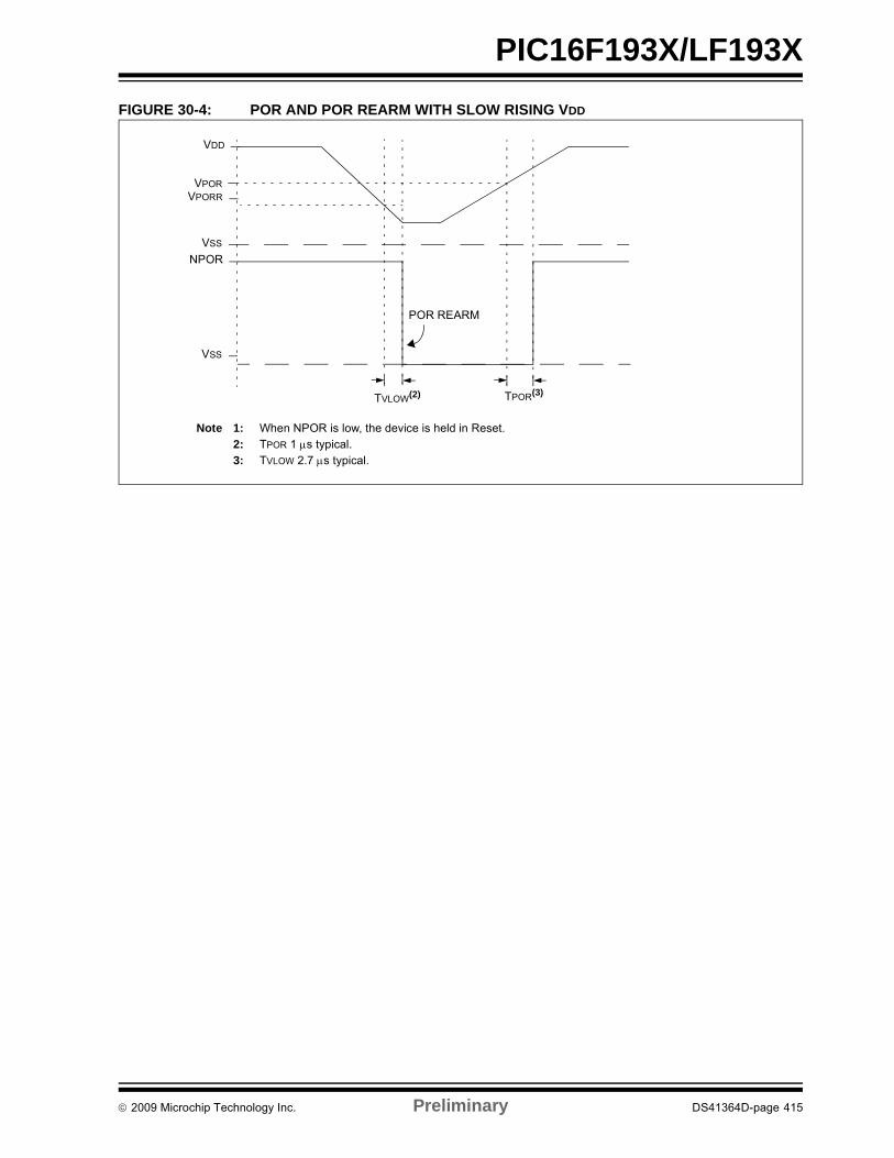
PIC16F193X/LF193X
FIGURE 30-4: POR AND POR REARM WITH SLOW RISING VDD
VDD
VPOR
VPORR
VSS
VSS
NPOR
TPOR(3)
POR REARM
Note 1: When NPOR is low, the device is held in Reset.2: TPOR 1 s typical.3: TVLOW 2.7 s typical.
TVLOW(2)
2009 Microchip Technology Inc. Preliminary DS41364D-page 415
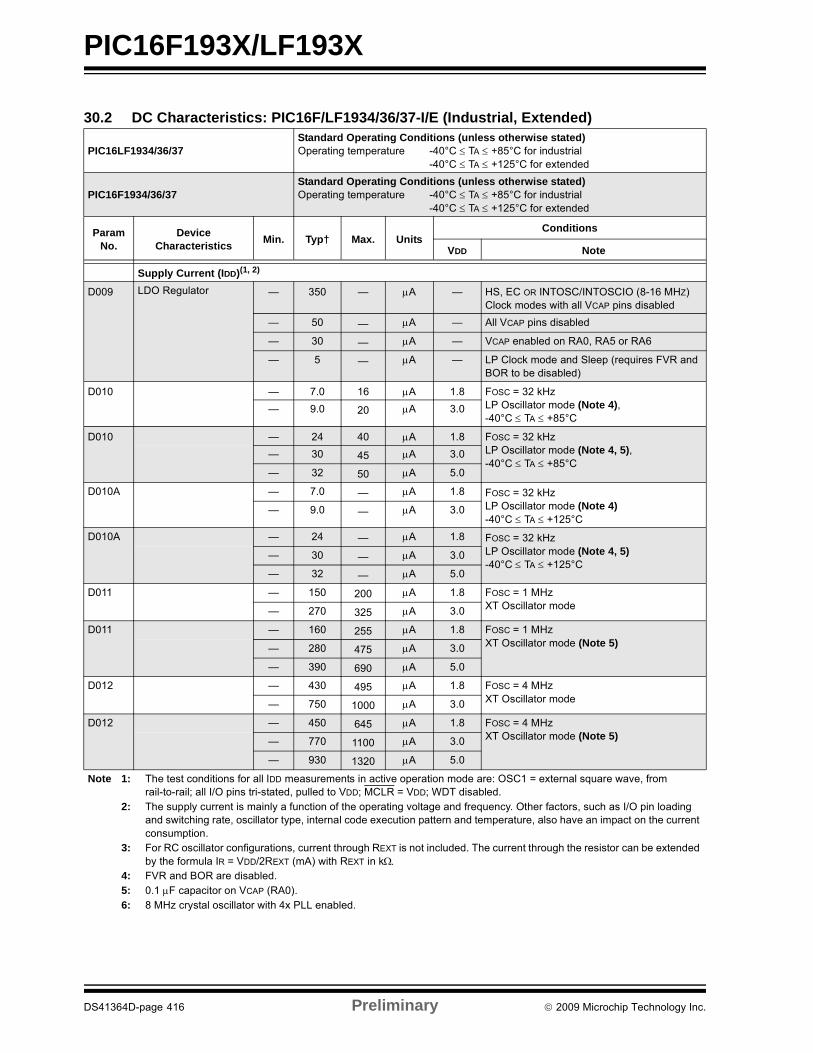
PIC16F193X/LF193X
30.2 DC Characteristics: PIC16F/LF1934/36/37-I/E (Industrial, Extended)
PIC16LF1934/36/37Standard Operating Conditions (unless otherwise stated)Operating temperature -40°C TA +85°C for industrial
-40°C TA +125°C for extended
PIC16F1934/36/37Standard Operating Conditions (unless otherwise stated)Operating temperature -40°C TA +85°C for industrial
-40°C TA +125°C for extended
ParamNo.
Device Characteristics
Min. Typ† Max. UnitsConditions
VDD Note
Supply Current (IDD)(1, 2)
D009 LDO Regulator — 350 — A — HS, EC OR INTOSC/INTOSCIO (8-16 MHZ) Clock modes with all VCAP pins disabled
— 50 — A — All VCAP pins disabled
— 30 — A — VCAP enabled on RA0, RA5 or RA6
— 5 — A — LP Clock mode and Sleep (requires FVR and BOR to be disabled)
D010 — 7.0 16 A 1.8 FOSC = 32 kHzLP Oscillator mode (Note 4),-40°C TA +85°C
— 9.0 20 A 3.0
D010 — 24 40 A 1.8 FOSC = 32 kHzLP Oscillator mode (Note 4, 5),-40°C TA +85°C
— 30 45 A 3.0
— 32 50 A 5.0
D010A — 7.0 — A 1.8 FOSC = 32 kHzLP Oscillator mode (Note 4)-40°C TA +125°C
— 9.0 — A 3.0
D010A — 24 — A 1.8 FOSC = 32 kHzLP Oscillator mode (Note 4, 5)-40°C TA +125°C
— 30 — A 3.0
— 32 — A 5.0
D011 — 150 200 A 1.8 FOSC = 1 MHzXT Oscillator mode— 270 325 A 3.0
D011 — 160 255 A 1.8 FOSC = 1 MHzXT Oscillator mode (Note 5)— 280 475 A 3.0
— 390 690 A 5.0
D012 — 430 495 A 1.8 FOSC = 4 MHzXT Oscillator mode— 750 1000 A 3.0
D012 — 450 645 A 1.8 FOSC = 4 MHzXT Oscillator mode (Note 5)— 770 1100 A 3.0
— 930 1320 A 5.0
Note 1: The test conditions for all IDD measurements in active operation mode are: OSC1 = external square wave, from rail-to-rail; all I/O pins tri-stated, pulled to VDD; MCLR = VDD; WDT disabled.
2: The supply current is mainly a function of the operating voltage and frequency. Other factors, such as I/O pin loading and switching rate, oscillator type, internal code execution pattern and temperature, also have an impact on the current consumption.
3: For RC oscillator configurations, current through REXT is not included. The current through the resistor can be extended by the formula IR = VDD/2REXT (mA) with REXT in k
4: FVR and BOR are disabled.5: 0.1 F capacitor on VCAP (RA0).6: 8 MHz crystal oscillator with 4x PLL enabled.
DS41364D-page 416 Preliminary 2009 Microchip Technology Inc.
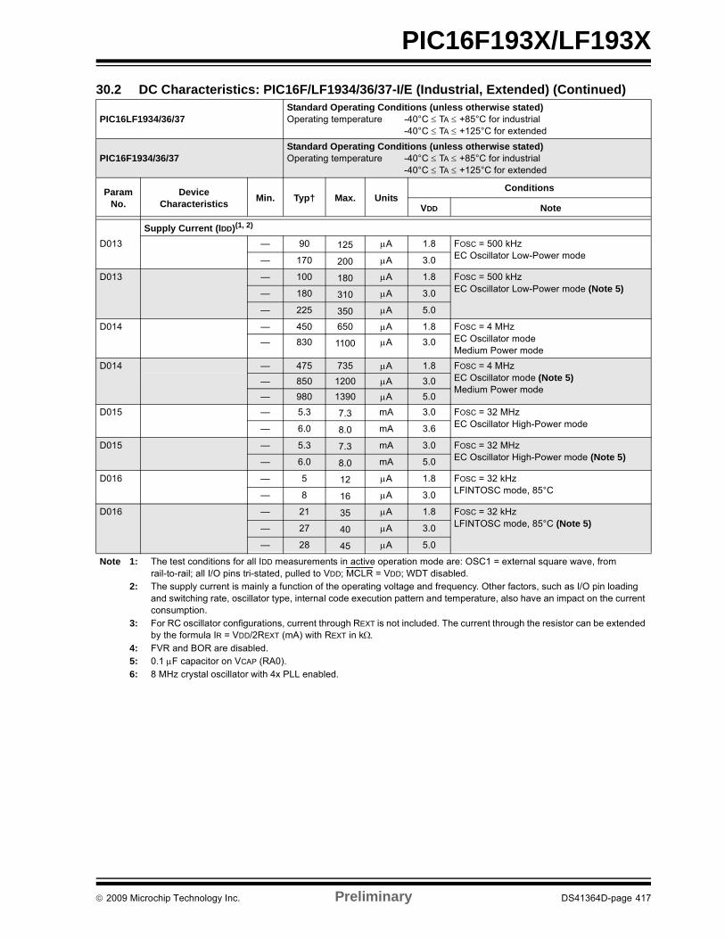
PIC16F193X/LF193X
Supply Current (IDD)(1, 2)
D013 — 90 125 A 1.8 FOSC = 500 kHzEC Oscillator Low-Power mode— 170 200 A 3.0
D013 — 100 180 A 1.8 FOSC = 500 kHzEC Oscillator Low-Power mode (Note 5)— 180 310 A 3.0
— 225 350 A 5.0
D014 — 450 650 A 1.8 FOSC = 4 MHzEC Oscillator modeMedium Power mode
— 830 1100 A 3.0
D014 — 475 735 A 1.8 FOSC = 4 MHzEC Oscillator mode (Note 5)Medium Power mode
— 850 1200 A 3.0
— 980 1390 A 5.0
D015 — 5.3 7.3 mA 3.0 FOSC = 32 MHzEC Oscillator High-Power mode— 6.0 8.0 mA 3.6
D015 — 5.3 7.3 mA 3.0 FOSC = 32 MHzEC Oscillator High-Power mode (Note 5)— 6.0 8.0 mA 5.0
D016 — 5 12 A 1.8 FOSC = 32 kHzLFINTOSC mode, 85°C— 8 16 A 3.0
D016 — 21 35 A 1.8 FOSC = 32 kHzLFINTOSC mode, 85°C (Note 5)— 27 40 A 3.0
— 28 45 A 5.0
30.2 DC Characteristics: PIC16F/LF1934/36/37-I/E (Industrial, Extended) (Continued)
PIC16LF1934/36/37Standard Operating Conditions (unless otherwise stated)Operating temperature -40°C TA +85°C for industrial
-40°C TA +125°C for extended
PIC16F1934/36/37Standard Operating Conditions (unless otherwise stated)Operating temperature -40°C TA +85°C for industrial
-40°C TA +125°C for extended
ParamNo.
Device Characteristics
Min. Typ† Max. UnitsConditions
VDD Note
Note 1: The test conditions for all IDD measurements in active operation mode are: OSC1 = external square wave, from rail-to-rail; all I/O pins tri-stated, pulled to VDD; MCLR = VDD; WDT disabled.
2: The supply current is mainly a function of the operating voltage and frequency. Other factors, such as I/O pin loading and switching rate, oscillator type, internal code execution pattern and temperature, also have an impact on the current consumption.
3: For RC oscillator configurations, current through REXT is not included. The current through the resistor can be extended by the formula IR = VDD/2REXT (mA) with REXT in k
4: FVR and BOR are disabled.5: 0.1 F capacitor on VCAP (RA0).6: 8 MHz crystal oscillator with 4x PLL enabled.
2009 Microchip Technology Inc. Preliminary DS41364D-page 417
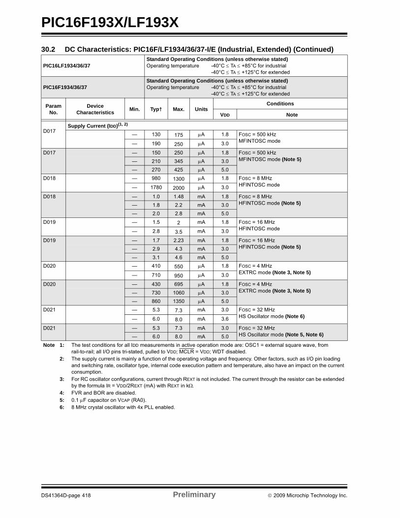
PIC16F193X/LF193X
D017Supply Current (IDD)(1, 2)
— 130 175 A 1.8 FOSC = 500 kHzMFINTOSC mode— 190 250 A 3.0
D017 — 150 250 A 1.8 FOSC = 500 kHzMFINTOSC mode (Note 5)— 210 345 A 3.0
— 270 425 A 5.0
D018 — 980 1300 A 1.8 FOSC = 8 MHzHFINTOSC mode— 1780 2000 A 3.0
D018 — 1.0 1.48 mA 1.8 FOSC = 8 MHzHFINTOSC mode (Note 5)— 1.8 2.2 mA 3.0
— 2.0 2.8 mA 5.0
D019 — 1.5 2 mA 1.8 FOSC = 16 MHzHFINTOSC mode— 2.8 3.5 mA 3.0
D019 — 1.7 2.23 mA 1.8 FOSC = 16 MHzHFINTOSC mode (Note 5)— 2.9 4.3 mA 3.0
— 3.1 4.6 mA 5.0
D020 — 410 550 A 1.8 FOSC = 4 MHzEXTRC mode (Note 3, Note 5)— 710 950 A 3.0
D020 — 430 695 A 1.8 FOSC = 4 MHzEXTRC mode (Note 3, Note 5)— 730 1060 A 3.0
— 860 1350 A 5.0
D021 — 5.3 7.3 mA 3.0 FOSC = 32 MHzHS Oscillator mode (Note 6)— 6.0 8.0 mA 3.6
D021 — 5.3 7.3 mA 3.0 FOSC = 32 MHzHS Oscillator mode (Note 5, Note 6)— 6.0 8.0 mA 5.0
30.2 DC Characteristics: PIC16F/LF1934/36/37-I/E (Industrial, Extended) (Continued)
PIC16LF1934/36/37Standard Operating Conditions (unless otherwise stated)Operating temperature -40°C TA +85°C for industrial
-40°C TA +125°C for extended
PIC16F1934/36/37Standard Operating Conditions (unless otherwise stated)Operating temperature -40°C TA +85°C for industrial
-40°C TA +125°C for extended
ParamNo.
Device Characteristics
Min. Typ† Max. UnitsConditions
VDD Note
Note 1: The test conditions for all IDD measurements in active operation mode are: OSC1 = external square wave, from rail-to-rail; all I/O pins tri-stated, pulled to VDD; MCLR = VDD; WDT disabled.
2: The supply current is mainly a function of the operating voltage and frequency. Other factors, such as I/O pin loading and switching rate, oscillator type, internal code execution pattern and temperature, also have an impact on the current consumption.
3: For RC oscillator configurations, current through REXT is not included. The current through the resistor can be extended by the formula IR = VDD/2REXT (mA) with REXT in k
4: FVR and BOR are disabled.5: 0.1 F capacitor on VCAP (RA0).6: 8 MHz crystal oscillator with 4x PLL enabled.
DS41364D-page 418 Preliminary 2009 Microchip Technology Inc.

PIC16F193X/LF193X
30.3 DC Characteristics: PIC16F/LF1934/36/37-I/E (Power-Down)
PIC16LF1934/36/37Standard Operating Conditions (unless otherwise stated)Operating temperature -40°C TA +85°C for industrial
-40°C TA +125°C for extended
PIC16F1934/36/37Standard Operating Conditions (unless otherwise stated)Operating temperature -40°C TA +85°C for industrial
-40°C TA +125°C for extended
ParamNo.
Device Characteristics Min. Typ†Max.
+85°CMax.
+125°CUnits
Conditions
VDD Note
Power-down Base Current (IPD)(2)
D023 — 0.06 1 — A 1.8 WDT, BOR, FVR, and T1OSC disabled, all Peripherals Inactive— 0.08 2 — A 3.0
D023 — 15 35 — A 1.8 WDT, BOR, FVR, and T1OSC disabled, all Peripherals Inactive— 18 40 — A 3.0
— 19 45 — A 5.0
D024 — 0.5 6 — A 1.8 LPWDT Current (Note 1)
— 0.8 7 — A 3.0
D024 — 16 35 — A 1.8 LPWDT Current (Note 1)
— 19 40 — A 3.0
— 20 45 — A 5.0
D025 — 8.5 23 — A 1.8 FVR current
— 8.5 26 — A 3.0
D025 — 32 50 — A 1.8 FVR current (Note 4)
— 39 72 — A 3.0
— 70 120 — A 5.0
D026 — 7.5 TBD — A 3.0 BOR Current (Note 1)
D026 — 34 57 — A 3.0 BOR Current (Note 1, Note 4)
— 67 100 — A 5.0
D027 — 0.6 5 — A 1.8 T1OSC Current (Note 1)
— 1.8 6 — A 3.0
D027 — 16 35 — A 1.8 T1OSC Current (Note 1)
— 21 40 — A 3.0
— 25 45 — A 5.0
* These parameters are characterized but not tested.† Data in “Typ” column is at 3.0V, 25°C unless otherwise stated. These parameters are for design guidance only and are
not tested.Legend: TBD = To Be DeterminedNote 1: The peripheral current is the sum of the base IDD or IPD and the additional current consumed when this peripheral is
enabled. The peripheral current can be determined by subtracting the base IDD or IPD current from this limit. Max values should be used when calculating total current consumption.
2: The power-down current in Sleep mode does not depend on the oscillator type. Power-down current is measured with the part in Sleep mode, with all I/O pins in high-impedance state and tied to VDD.
3: A/D oscillator source is FRC.4: 0.1 F capacitor on VCAP (RA0).
2009 Microchip Technology Inc. Preliminary DS41364D-page 419

PIC16F193X/LF193X
Power-down Base Current (IPD)(2)
D028 — 0.1 5 — A 1.8 A/D Current (Note 1, Note 3), no conversion in progress— 0.1 6 — A 3.0
D028 — 16 35 — A 1.8 A/D Current (Note 1, Note 3), no conversion in progress— 21 40 — A 3.0
— 25 50 — A 5.0
D029 — 250 — — A 1.8 A/D Current (Note 1, Note 3), conversion in progress— 250 — — A 3.0
D029 — 280 — — A 1.8 A/D Current (Note 1, Note 3, Note 4), conversion in progress— 280 — — A 3.0
— 280 — — A 5.0
D030 — 3.5 7 — A 1.8 Cap Sense, Low Power mode
— 7 9 — A 3.0
D030 — 17 38 — A 1.8 Cap Sense, Low Power mode
— 21 50 — A 3.0
— 22 70 — A 5.0
D031 — 1 — — A 3.6 LCD Bias Ladder, Low-power
— 10 — — A 3.6 LCD Bias Ladder, Medium-power
— 100 — — A 3.6 LCD Bias Ladder, High-power
D031 — 1 — — A 5.0 LCD Bias Ladder, Low-power
— 10 — — A 5.0 LCD Bias Ladder, Medium-power
— 100 — — A 5.0 LCD Bias Ladder, High-power
30.3 DC Characteristics: PIC16F/LF1934/36/37-I/E (Power-Down) (Continued)
PIC16LF1934/36/37Standard Operating Conditions (unless otherwise stated)Operating temperature -40°C TA +85°C for industrial
-40°C TA +125°C for extended
PIC16F1934/36/37Standard Operating Conditions (unless otherwise stated)Operating temperature -40°C TA +85°C for industrial
-40°C TA +125°C for extended
ParamNo.
Device Characteristics Min. Typ†Max.
+85°CMax.
+125°CUnits
Conditions
VDD Note
* These parameters are characterized but not tested.† Data in “Typ” column is at 3.0V, 25°C unless otherwise stated. These parameters are for design guidance only and are
not tested.Legend: TBD = To Be DeterminedNote 1: The peripheral current is the sum of the base IDD or IPD and the additional current consumed when this peripheral is
enabled. The peripheral current can be determined by subtracting the base IDD or IPD current from this limit. Max values should be used when calculating total current consumption.
2: The power-down current in Sleep mode does not depend on the oscillator type. Power-down current is measured with the part in Sleep mode, with all I/O pins in high-impedance state and tied to VDD.
3: A/D oscillator source is FRC.4: 0.1 F capacitor on VCAP (RA0).
DS41364D-page 420 Preliminary 2009 Microchip Technology Inc.

PIC16F193X/LF193X
30.4 DC Characteristics: PIC16F/LF1934/36/37-I/E
DC CHARACTERISTICSStandard Operating Conditions (unless otherwise stated)Operating temperature -40°C TA +85°C for industrial
-40°C TA +125°C for extended
ParamNo.
Sym. Characteristic Min. Typ† Max. Units Conditions
VIL Input Low Voltage
I/O PORT:
D032 with TTL buffer — — 0.8 V 4.5V VDD 5.5V
D032A — — 0.15 VDD V 1.8V VDD 4.5V
D033 with Schmitt Trigger buffer — — 0.2 VDD V 2.0V VDD 5.5V
with I2C™ levels — — 0.3 VDD V
with SMBus levels — — 0.8 V 2.7V VDD 5.5V
D034 MCLR, OSC1 (RC mode)(1) — — 0.2 VDD V
D034A OSC1 (HS mode) — — 0.3 VDD V
VIH Input High Voltage
I/O ports:
D040 with TTL buffer 2.0 — — V 4.5V VDD 5.5V
D040A 0.25 VDD + 0.8
— — V 1.8V VDD 4.5V
D041 with Schmitt Trigger buffer 0.8 VDD — — V 2.0V VDD 5.5V
with I2C™ levels 0.7 VDD — — V
with SMBus levels 2.1 — — V 2.7V VDD 5.5V
D042 MCLR 0.8 VDD — — V
D043A OSC1 (HS mode) 0.7 VDD — — V
D043B OSC1 (RC mode) 0.9 VDD — — V (Note 1)
IIL Input Leakage Current(2)
D060 I/O ports — ± 5
± 5
± 125
± 1000
nA
nA
VSS VPIN VDD, Pin at high-impedance @ 85°C125°C
D061 MCLR(3) — ± 50 ± 200 nA VSS VPIN VDD @ 85°C
IPUR Weak Pull-up Current
D070* 2525
100140
200300 A
VDD = 3.3V, VPIN = VSS
VDD = 5.0V, VPIN = VSS
VOL Output Low Voltage(4)
D080 I/O ports— — 0.6 V
IOL = 8mA, VDD = 5VIOL = 6mA, VDD = 3.3VIOL = 1.8mA, VDD = 1.8V
VOH Output High Voltage(4)
D090 I/O portsVDD - 0.7 — — V
IOH = 3.5mA, VDD = 5VIOH = 3mA, VDD = 3.3VIOH = 1mA, VDD = 1.8V
Legend: TBD = To Be Determined* These parameters are characterized but not tested.† Data in “Typ” column is at 3.0V, 25°C unless otherwise stated. These parameters are for design guidance only and are
not tested.Note 1: In RC oscillator configuration, the OSC1/CLKIN pin is a Schmitt Trigger input. It is not recommended to use an external
clock in RC mode.2: Negative current is defined as current sourced by the pin.3: The leakage current on the MCLR pin is strongly dependent on the applied voltage level. The specified levels represent
normal operating conditions. Higher leakage current may be measured at different input voltages.4: Including OSC2 in CLKOUT mode.
2009 Microchip Technology Inc. Preliminary DS41364D-page 421

PIC16F193X/LF193X
Capacitive Loading Specs on Output Pins
D101* COSC2 OSC2 pin — — 15 pF In XT, HS and LP modes when external clock is used to drive OSC1
D101A* CIO All I/O pins — — 50 pF
VCAP Capacitor Charging
D102 Charging current — 200 — A
D102A Source/sink capability when charging complete
— 0.0 — mA
30.4 DC Characteristics: PIC16F/LF1934/36/37-I/E (Continued)
DC CHARACTERISTICSStandard Operating Conditions (unless otherwise stated)Operating temperature -40°C TA +85°C for industrial
-40°C TA +125°C for extended
ParamNo.
Sym. Characteristic Min. Typ† Max. Units Conditions
Legend: TBD = To Be Determined* These parameters are characterized but not tested.† Data in “Typ” column is at 3.0V, 25°C unless otherwise stated. These parameters are for design guidance only and are
not tested.Note 1: In RC oscillator configuration, the OSC1/CLKIN pin is a Schmitt Trigger input. It is not recommended to use an external
clock in RC mode.2: Negative current is defined as current sourced by the pin.3: The leakage current on the MCLR pin is strongly dependent on the applied voltage level. The specified levels represent
normal operating conditions. Higher leakage current may be measured at different input voltages.4: Including OSC2 in CLKOUT mode.
DS41364D-page 422 Preliminary 2009 Microchip Technology Inc.

PIC16F193X/LF193X
30.5 Memory Programming Requirements
DC CHARACTERISTICSStandard Operating Conditions (unless otherwise stated)Operating temperature -40°C TA +125°C
ParamNo.
Sym. Characteristic Min. Typ† Max. Units Conditions
Program Memory Programming Specifications
D110 VIHH Voltage on MCLR/VPP/RE3 pin 8.0 — 9.0 V (Note 3, Note 4)
D111 IDDP Supply Current during Programming
— — 10 mA
D112 VDD for Bulk Erase 2.7 — VDD
max.V
D113 VPEW VDD for Write or Row Erase VDD
min.— VDD
max.V
D114 IPPPGM Current on MCLR/VPP during Erase/Write
— — 1.0 mA
D115 IDDPGM Current on VDD during Erase/Write — 5.0 mA
Data EEPROM Memory
D116 ED Byte Endurance 100K — — E/W -40C to +85C
D117 VDRW VDD for Read/Write VDD
min.— VDD
max.V
D118 TDEW Erase/Write Cycle Time — 4.0 5.0 ms
D119 TRETD Characteristic Retention 40 — — Year Provided no other specifications are violated
D120 TREF Number of Total Erase/Write Cycles before Refresh(2)
1M 10M — E/W -40°C to +85°C
Program Flash Memory
D121 EP Cell Endurance 10K — — E/W -40C to +85C (Note 1)
D122 VPR VDD for Read VDD
min.— VDD
max.V
D123 TIW Self-timed Write Cycle Time — 2 2.5 ms
D124 TRETD Characteristic Retention 40 — — Year Provided no other specifications are violated
† Data in “Typ” column is at 3.0V, 25°C unless otherwise stated. These parameters are for design guidance only and are not tested.
Note 1: Self-write and Block Erase.2: Refer to Section 11.2 “Using the Data EEPROM” for a more detailed discussion on data EEPROM
endurance.3: Required only if single-supply programming is disabled.4: The MPLAB ICD 2 does not support variable VPP output. Circuitry to limit the ICD 2 VPP voltage must be
placed between the ICD 2 and target system when programming or debugging with the ICD 2.
2009 Microchip Technology Inc. Preliminary DS41364D-page 423

PIC16F193X/LF193X
30.6 Thermal Considerations
Standard Operating Conditions (unless otherwise stated)Operating temperature -40°C TA +125°C
ParamNo.
Sym. Characteristic Typ. Units Conditions
TH01 JA Thermal Resistance Junction to Ambient 60 C/W 28-pin SPDIP package
80 C/W 28-pin SOIC package
90 C/W 28-pin SSOP package
27.5 C/W 28-pin UQFN 4x4mm package
27.5 C/W 28-pin QFN 6x6mm package
47.2 C/W 40-pin PDIP package
46 C/W 44-pin TQFP package
24.4 C/W 44-pin QFN 8x8mm package
TH02 JC Thermal Resistance Junction to Case 31.4 C/W 28-pin SPDIP package
24 C/W 28-pin SOIC package
24 C/W 28-pin SSOP package
24 C/W 28-pin UQFN 4x4mm package
24 C/W 28-pin QFN 6x6mm package
24.7 C/W 40-pin PDIP package
14.5 C/W 44-pin TQFP package
20 C/W 44-pin QFN 8x8mm package
TH03 TJMAX Maximum Junction Temperature 150 CTH04 PD Power Dissipation — W PD = PINTERNAL + PI/O
TH05 PINTERNAL Internal Power Dissipation — W PINTERNAL = IDD x VDD(1)
TH06 PI/O I/O Power Dissipation — W PI/O = (IOL * VOL) + (IOH * (VDD - VOH))
TH07 PDER Derated Power — W PDER = PDMAX (TJ - TA)/JA(2)
Note 1: IDD is current to run the chip alone without driving any load on the output pins.2: TA = Ambient Temperature3: TJ = Junction Temperature
DS41364D-page 424 Preliminary 2009 Microchip Technology Inc.
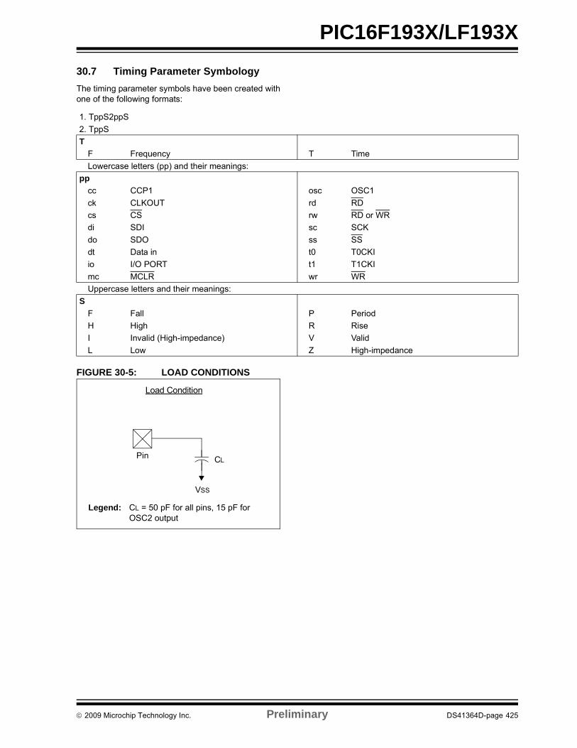
PIC16F193X/LF193X
30.7 Timing Parameter Symbology
The timing parameter symbols have been created withone of the following formats:
FIGURE 30-5: LOAD CONDITIONS
1. TppS2ppS
2. TppS
T
F Frequency T Time
Lowercase letters (pp) and their meanings:
pp
cc CCP1 osc OSC1
ck CLKOUT rd RD
cs CS rw RD or WR
di SDI sc SCK
do SDO ss SS
dt Data in t0 T0CKI
io I/O PORT t1 T1CKI
mc MCLR wr WR
Uppercase letters and their meanings:
S
F Fall P Period
H High R Rise
I Invalid (High-impedance) V Valid
L Low Z High-impedance
VSS
CL
Legend: CL = 50 pF for all pins, 15 pF for OSC2 output
Load Condition
Pin
2009 Microchip Technology Inc. Preliminary DS41364D-page 425

PIC16F193X/LF193X
30.8 AC Characteristics: PIC16F/LF1934/36/37-I/E
FIGURE 30-6: CLOCK TIMING
TABLE 30-1: CLOCK OSCILLATOR TIMING REQUIREMENTS
OSC1/CLKIN
OSC2/CLKOUT
Q4 Q1 Q2 Q3 Q4 Q1
OS02
OS03OS04 OS04
OSC2/CLKOUT(LP,XT,HS Modes)
(CLKOUT Mode)
Standard Operating Conditions (unless otherwise stated)Operating temperature -40°C TA +125°C
ParamNo.
Sym. Characteristic Min. Typ† Max. Units Conditions
OS01 FOSC External CLKIN Frequency(1) DC — 0.5 MHz EC Oscillator mode (low)
DC — 4 MHz EC Oscillator mode (medium)
DC — 32 MHz EC Oscillator mode (high)
Oscillator Frequency(1) — 32.768 — kHz LP Oscillator mode
0.1 — 4 MHz XT Oscillator mode
1 — 4 MHz HS Oscillator mode, VDD 2.7V
1 — 20 MHz HS Oscillator mode, VDD > 2.7V
DC — 4 MHz RC Oscillator mode
OS02 TOSC External CLKIN Period(1) 27 — s LP Oscillator mode
250 — ns XT Oscillator mode
50 — ns HS Oscillator mode
31.25 — ns EC Oscillator mode
Oscillator Period(1) — 30.5 — s LP Oscillator mode
250 — 10,000 ns XT Oscillator mode
50 — 1,000 ns HS Oscillator mode
250 — — ns RC Oscillator mode
OS03 TCY Instruction Cycle Time(1) 200 TCY DC ns TCY = 4/FOSC
OS04* TosH,TosL
External CLKIN High,External CLKIN Low
2 — — s LP oscillator
100 — — ns XT oscillator
20 — — ns HS oscillator
OS05* TosR,TosF
External CLKIN Rise,External CLKIN Fall
0 — ns LP oscillator
0 — ns XT oscillator
0 — ns HS oscillator
* These parameters are characterized but not tested.† Data in “Typ” column is at 3.0V, 25°C unless otherwise stated. These parameters are for design guidance only and are not
tested.Note 1: Instruction cycle period (TCY) equals four times the input oscillator time base period. All specified values are based on
characterization data for that particular oscillator type under standard operating conditions with the device executing code. Exceeding these specified limits may result in an unstable oscillator operation and/or higher than expected current con-sumption. All devices are tested to operate at “min” values with an external clock applied to OSC1 pin. When an external clock input is used, the “max” cycle time limit is “DC” (no clock) for all devices.
DS41364D-page 426 Preliminary 2009 Microchip Technology Inc.
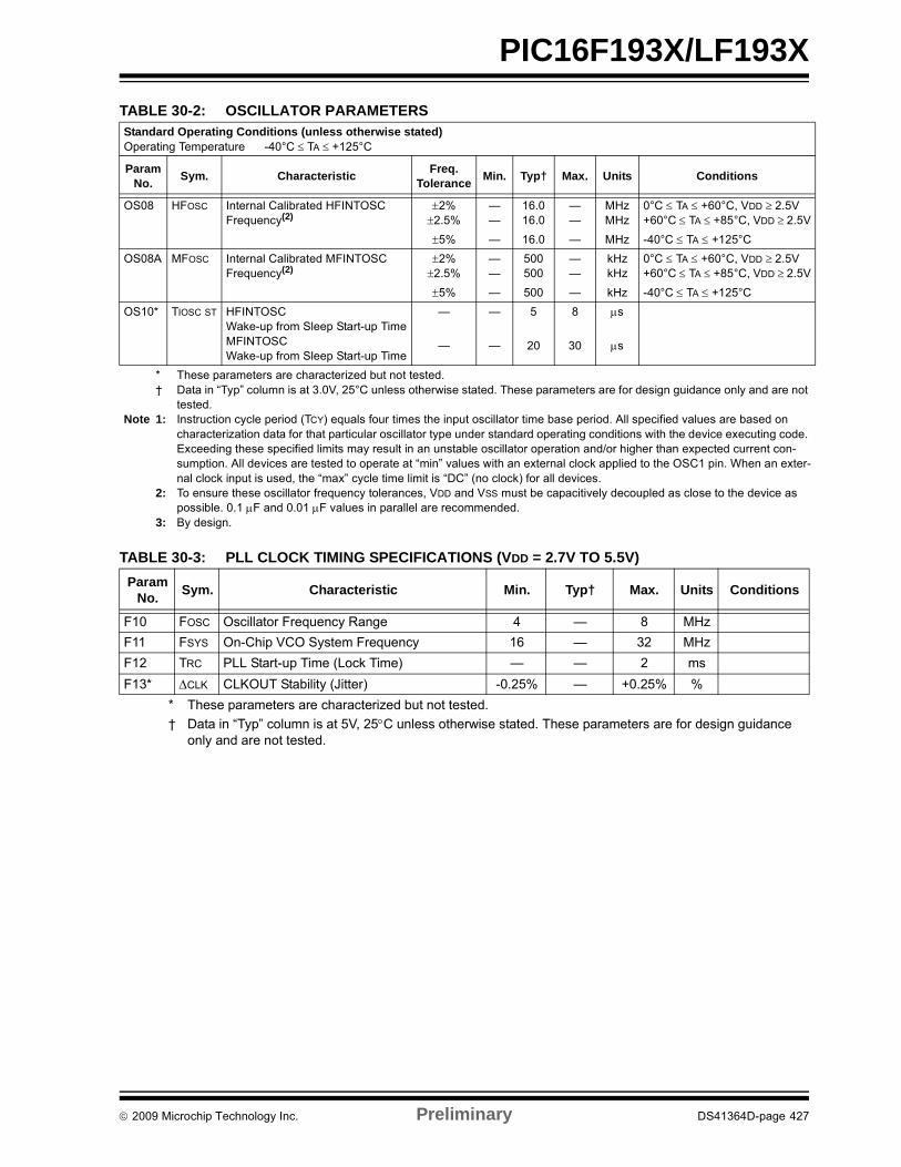
PIC16F193X/LF193X
TABLE 30-2: OSCILLATOR PARAMETERS
TABLE 30-3: PLL CLOCK TIMING SPECIFICATIONS (VDD = 2.7V TO 5.5V)
Standard Operating Conditions (unless otherwise stated)Operating Temperature -40°C TA +125°C
Param No.
Sym. CharacteristicFreq.
ToleranceMin. Typ† Max. Units Conditions
OS08 HFOSC Internal Calibrated HFINTOSC Frequency(2)
2%2.5%
——
16.016.0
——
MHzMHz
0°C TA +60°C, VDD 2.5V+60°C TA +85°C, VDD 2.5V
5% — 16.0 — MHz -40°C TA +125°C
OS08A MFOSC Internal Calibrated MFINTOSC Frequency(2)
2%2.5%
——
500500
——
kHzkHz
0°C TA +60°C, VDD 2.5V+60°C TA +85°C, VDD 2.5V
5% — 500 — kHz -40°C TA +125°C
OS10* TIOSC ST HFINTOSCWake-up from Sleep Start-up TimeMFINTOSCWake-up from Sleep Start-up Time
— — 5 8 s
— — 20 30 s
* These parameters are characterized but not tested.† Data in “Typ” column is at 3.0V, 25°C unless otherwise stated. These parameters are for design guidance only and are not
tested.Note 1: Instruction cycle period (TCY) equals four times the input oscillator time base period. All specified values are based on
characterization data for that particular oscillator type under standard operating conditions with the device executing code. Exceeding these specified limits may result in an unstable oscillator operation and/or higher than expected current con-sumption. All devices are tested to operate at “min” values with an external clock applied to the OSC1 pin. When an exter-nal clock input is used, the “max” cycle time limit is “DC” (no clock) for all devices.
2: To ensure these oscillator frequency tolerances, VDD and VSS must be capacitively decoupled as close to the device as possible. 0.1 F and 0.01 F values in parallel are recommended.
3: By design.
Param No.
Sym. Characteristic Min. Typ† Max. Units Conditions
F10 FOSC Oscillator Frequency Range 4 — 8 MHz
F11 FSYS On-Chip VCO System Frequency 16 — 32 MHz
F12 TRC PLL Start-up Time (Lock Time) — — 2 ms
F13* CLK CLKOUT Stability (Jitter) -0.25% — +0.25% %
* These parameters are characterized but not tested.
† Data in “Typ” column is at 5V, 25C unless otherwise stated. These parameters are for design guidance only and are not tested.
2009 Microchip Technology Inc. Preliminary DS41364D-page 427

PIC16F193X/LF193X
FIGURE 30-7: CLKOUT AND I/O TIMING
FOSC
CLKOUT
I/O pin(Input)
I/O pin(Output)
Q4 Q1 Q2 Q3
OS11
OS19
OS13
OS15
OS18, OS19
OS20OS21
OS17
OS16
OS14
OS12
OS18
Old Value New Value
Write Fetch Read ExecuteCycle
DS41364D-page 428 Preliminary 2009 Microchip Technology Inc.

PIC16F193X/LF193X
TABLE 30-4: CLKOUT AND I/O TIMING PARAMETERS
FIGURE 30-8: RESET, WATCHDOG TIMER, OSCILLATOR START-UP TIMER AND POWER-UP TIMER TIMING
Standard Operating Conditions (unless otherwise stated)Operating Temperature -40°C TA +125°C
Param No.
Sym. Characteristic Min. Typ† Max. Units Conditions
OS11 TosH2ckL FOSC to CLKOUT (1) — — 70 ns VDD = 3.3-5.0V
OS12 TosH2ckH FOSC to CLKOUT (1) — — 72 ns VDD = 3.3-5.0V
OS13 TckL2ioV CLKOUT to Port out valid(1) — — 20 ns
OS14 TioV2ckH Port input valid before CLKOUT(1) TOSC + 200 ns — — ns
OS15 TosH2ioV Fosc (Q1 cycle) to Port out valid — 50 70* ns VDD = 3.3-5.0V
OS16 TosH2ioI Fosc (Q2 cycle) to Port input invalid (I/O in hold time)
50 — — ns VDD = 3.3-5.0V
OS17 TioV2osH Port input valid to Fosc(Q2 cycle)(I/O in setup time)
20 — — ns
OS18 TioR Port output rise time(2) ——
4015
7232
ns VDD = 1.8VVDD = 3.3-5.0V
OS19 TioF Port output fall time(2) ——
2815
5530
ns VDD = 1.8VVDD = 3.3-5.0V
OS20* Tinp INT pin input high or low time 25 — — ns
OS21* Tioc Interrupt-on-change new input level time
25 — — ns
* These parameters are characterized but not tested.† Data in “Typ” column is at 3.0V, 25C unless otherwise stated.
Note 1: Measurements are taken in RC mode where CLKOUT output is 4 x TOSC.2: Includes OSC2 in CLKOUT mode.
VDD
MCLR
InternalPOR
PWRTTime-out
OSCStart-Up Time
Internal Reset(1)
Watchdog Timer
33
32
30
3134
I/O pins
34
Note 1: Asserted low.
Reset(1)
2009 Microchip Technology Inc. Preliminary DS41364D-page 429
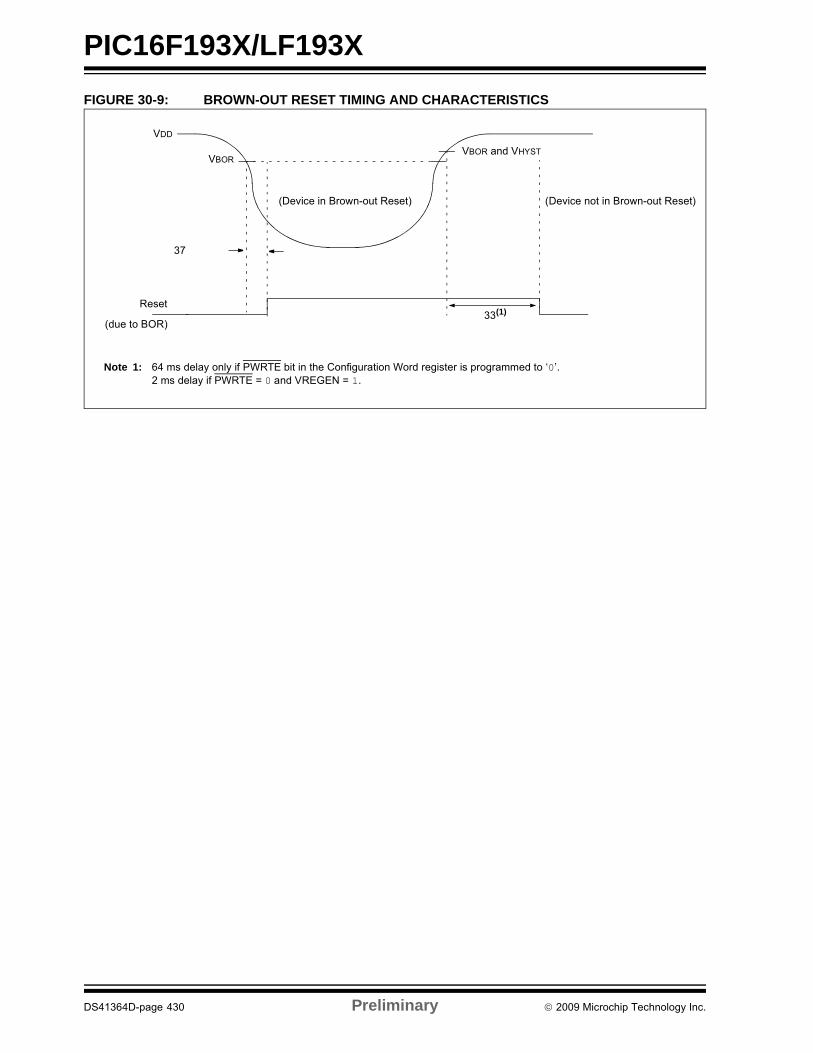
PIC16F193X/LF193X
FIGURE 30-9: BROWN-OUT RESET TIMING AND CHARACTERISTICS
VBOR
VDD
(Device in Brown-out Reset) (Device not in Brown-out Reset)
33(1)
Note 1: 64 ms delay only if PWRTE bit in the Configuration Word register is programmed to ‘0’. 2 ms delay if PWRTE = 0 and VREGEN = 1.
Reset
(due to BOR)
VBOR and VHYST
37
DS41364D-page 430 Preliminary 2009 Microchip Technology Inc.

PIC16F193X/LF193X
TABLE 30-5: RESET, WATCHDOG TIMER, OSCILLATOR START-UP TIMER, POWER-UP TIMER AND BROWN-OUT RESET PARAMETERS
FIGURE 30-10: TIMER0 AND TIMER1 EXTERNAL CLOCK TIMINGS
Standard Operating Conditions (unless otherwise stated)Operating Temperature -40°C TA +125°C
Param No.
Sym. Characteristic Min. Typ† Max. Units Conditions
30 TMCL MCLR Pulse Width (low) 2 5
——
——
ss
VDD = 3.3-5V, -40°C to +85°CVDD = 3.3-5V
31 TWDTLP Low-Power Watchdog Timer Time-out Period (No Prescaler)
10 18 27 ms VDD = 3.3V-5V
32 TOST Oscillator Start-up Timer Period(1), (2) — 1024 — Tosc (Note 3)
33* TPWRT Power-up Timer Period, PWRTE = 0 40 65 140 ms
34* TIOZ I/O high-impedance from MCLR Low or Watchdog Timer Reset
— — 2.0 s
35 VBOR Brown-out Reset Voltage 2.381.80
2.51.9
2.732.11
V BORV=2.5VBORV=1.9V
36* VHYST Brown-out Reset Hysteresis 0 25 50 mV -40°C to +85°C
37* TBORDC Brown-out Reset DC Response Time
1 3 5 s VDD VBOR
* These parameters are characterized but not tested.† Data in “Typ” column is at 3.0V, 25°C unless otherwise stated. These parameters are for design guidance
only and are not tested.Note 1: Instruction cycle period (TCY) equals four times the input oscillator time base period. All specified values are
based on characterization data for that particular oscillator type under standard operating conditions with the device executing code. Exceeding these specified limits may result in an unstable oscillator operation and/or higher than expected current consumption. All devices are tested to operate at “min” values with an external clock applied to the OSC1 pin. When an external clock input is used, the “max” cycle time limit is “DC” (no clock) for all devices.
2: By design.3: Period of the slower clock.4: To ensure these voltage tolerances, VDD and VSS must be capacitively decoupled as close to the device as
possible. 0.1 F and 0.01 F values in parallel are recommended.
T0CKI
T1CKI
40 41
42
45 46
47 49
TMR0 orTMR1
2009 Microchip Technology Inc. Preliminary DS41364D-page 431
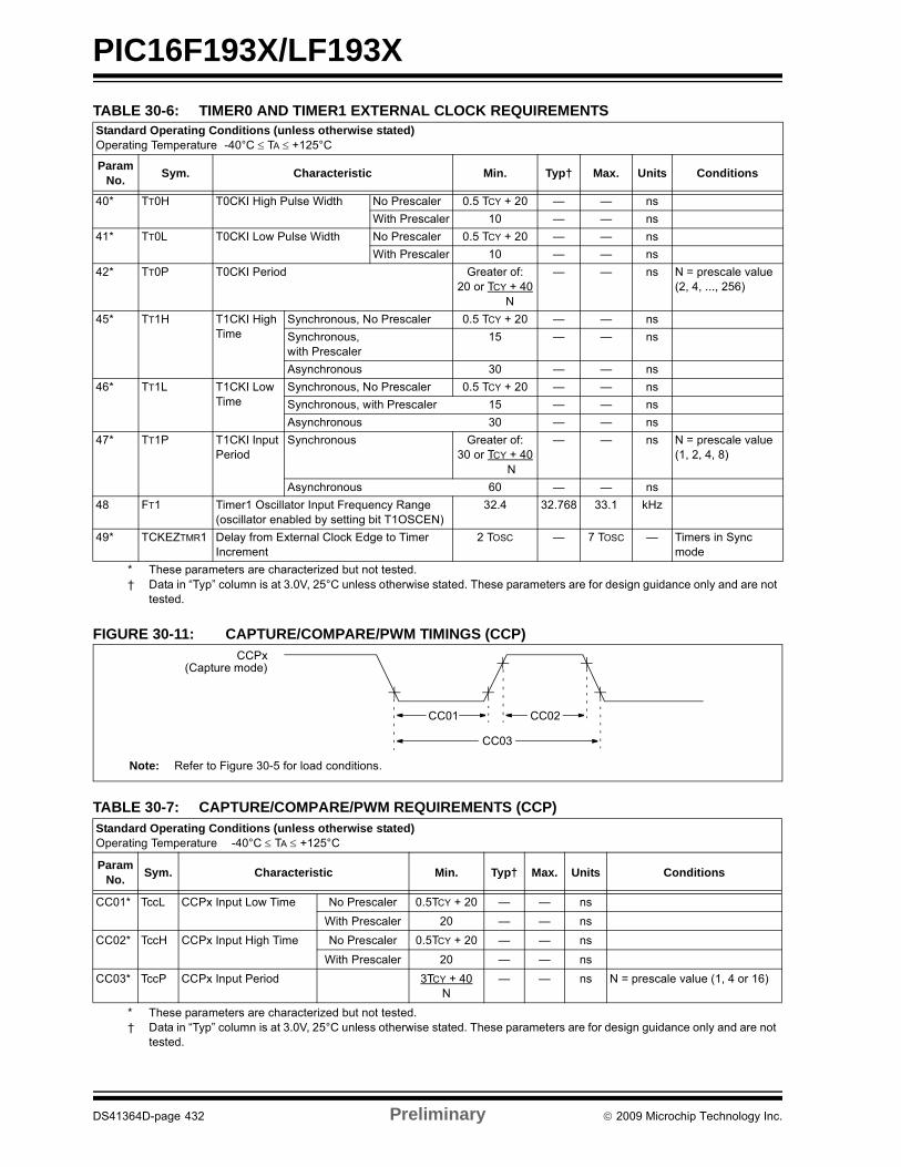
PIC16F193X/LF193X
TABLE 30-6: TIMER0 AND TIMER1 EXTERNAL CLOCK REQUIREMENTS
FIGURE 30-11: CAPTURE/COMPARE/PWM TIMINGS (CCP)
TABLE 30-7: CAPTURE/COMPARE/PWM REQUIREMENTS (CCP)
Standard Operating Conditions (unless otherwise stated)Operating Temperature -40°C TA +125°C
Param No.
Sym. Characteristic Min. Typ† Max. Units Conditions
40* TT0H T0CKI High Pulse Width No Prescaler 0.5 TCY + 20 — — ns
With Prescaler 10 — — ns
41* TT0L T0CKI Low Pulse Width No Prescaler 0.5 TCY + 20 — — ns
With Prescaler 10 — — ns
42* TT0P T0CKI Period Greater of:20 or TCY + 40
N
— — ns N = prescale value (2, 4, ..., 256)
45* TT1H T1CKI High Time
Synchronous, No Prescaler 0.5 TCY + 20 — — ns
Synchronous, with Prescaler
15 — — ns
Asynchronous 30 — — ns
46* TT1L T1CKI Low Time
Synchronous, No Prescaler 0.5 TCY + 20 — — ns
Synchronous, with Prescaler 15 — — ns
Asynchronous 30 — — ns
47* TT1P T1CKI Input Period
Synchronous Greater of:30 or TCY + 40
N
— — ns N = prescale value (1, 2, 4, 8)
Asynchronous 60 — — ns
48 FT1 Timer1 Oscillator Input Frequency Range (oscillator enabled by setting bit T1OSCEN)
32.4 32.768 33.1 kHz
49* TCKEZTMR1 Delay from External Clock Edge to Timer Increment
2 TOSC — 7 TOSC — Timers in Sync mode
* These parameters are characterized but not tested.† Data in “Typ” column is at 3.0V, 25°C unless otherwise stated. These parameters are for design guidance only and are not
tested.
Standard Operating Conditions (unless otherwise stated)Operating Temperature -40°C TA +125°C
Param No.
Sym. Characteristic Min. Typ† Max. Units Conditions
CC01* TccL CCPx Input Low Time No Prescaler 0.5TCY + 20 — — ns
With Prescaler 20 — — ns
CC02* TccH CCPx Input High Time No Prescaler 0.5TCY + 20 — — ns
With Prescaler 20 — — ns
CC03* TccP CCPx Input Period 3TCY + 40N
— — ns N = prescale value (1, 4 or 16)
* These parameters are characterized but not tested.† Data in “Typ” column is at 3.0V, 25°C unless otherwise stated. These parameters are for design guidance only and are not
tested.
Note: Refer to Figure 30-5 for load conditions.
(Capture mode)
CC01 CC02
CC03
CCPx
DS41364D-page 432 Preliminary 2009 Microchip Technology Inc.
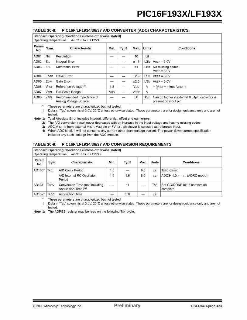
PIC16F193X/LF193X
TABLE 30-8: PIC16F/LF1934/36/37 A/D CONVERTER (ADC) CHARACTERISTICS:
TABLE 30-9: PIC16F/LF1934/36/37 A/D CONVERSION REQUIREMENTS
Standard Operating Conditions (unless otherwise stated)Operating temperature -40°C TA +125°C
Param No.
Sym. Characteristic Min. Typ† Max. Units Conditions
AD01 NR Resolution — — 10 bit
AD02 EIL Integral Error — — ±1.7 LSb VREF = 3.0V
AD03 EDL Differential Error — — ±1 LSb No missing codesVREF = 3.0V
AD04 EOFF Offset Error — — ±2.5 LSb VREF = 3.0V
AD05 EGN Gain Error — — ±2.0 LSb VREF = 3.0V
AD06 VREF Reference Voltage(3) 1.8 — VDD V = (VREF+ minus VREF-)
AD07 VAIN Full-Scale Range VSS — VREF V
AD08 ZAIN Recommended Impedance of Analog Voltage Source
— — 50 k Can go higher if external 0.01F capacitor is present on input pin.
* These parameters are characterized but not tested.† Data in “Typ” column is at 3.0V, 25°C unless otherwise stated. These parameters are for design guidance only and are not
tested.Note 1: Total Absolute Error includes integral, differential, offset and gain errors.
2: The A/D conversion result never decreases with an increase in the input voltage and has no missing codes.3: ADC VREF is from external VREF, VDD pin or FVREF, whichever is selected as reference input.4: When ADC is off, it will not consume any current other than leakage current. The power-down current specification
includes any such leakage from the ADC module.
Standard Operating Conditions (unless otherwise stated)Operating temperature -40°C TA +125°C
ParamNo.
Sym. Characteristic Min. Typ† Max. Units Conditions
AD130* TAD A/D Clock Period 1.0 — 9.0 s TOSC-based
A/D Internal RC Oscillator Period
1.0 1.6 6.0 s ADCS<1:0> = 11 (ADRC mode)
AD131 TCNV Conversion Time (not including Acquisition Time)(1)
— 11 — TAD Set GO/DONE bit to conversioncomplete
AD132* TACQ Acquisition Time — 5.0 — s
* These parameters are characterized but not tested.† Data in “Typ” column is at 3.0V, 25°C unless otherwise stated. These parameters are for design guidance only and are not
tested.Note 1: The ADRES register may be read on the following TCY cycle.
2009 Microchip Technology Inc. Preliminary DS41364D-page 433

PIC16F193X/LF193X
FIGURE 30-12: PIC16F/LF1934/36/37 A/D CONVERSION TIMING (NORMAL MODE)
FIGURE 30-13: PIC16F/LF1934/36/37 A/D CONVERSION TIMING (SLEEP MODE)
AD131
AD130
BSF ADCON0, GO
Q4
A/D CLK
A/D Data
ADRES
ADIF
GO
Sample
OLD_DATA
Sampling Stopped
DONE
NEW_DATA
7 6 5 3 2 1 0
Note 1: If the A/D clock source is selected as RC, a time of TCY is added before the A/D clock starts. This allows the SLEEP instruction to be executed.
1 TCY
4
AD134 (TOSC/2(1))
1 TCY
AD132
AD132
AD131
AD130
BSF ADCON0, GO
Q4
A/D CLK
A/D Data
ADRES
ADIF
GO
Sample
OLD_DATA
Sampling Stopped
DONE
NEW_DATA
7 5 3 2 1 0
Note 1: If the A/D clock source is selected as RC, a time of TCY is added before the A/D clock starts. This allows the SLEEP instruction to be executed.
AD134
46
1 TCY(TOSC/2 + TCY(1))
1 TCY
DS41364D-page 434 Preliminary 2009 Microchip Technology Inc.
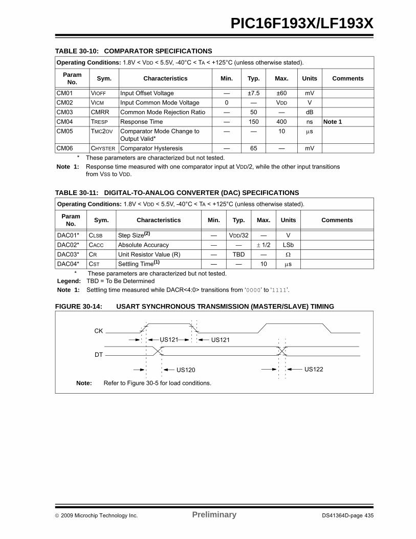
PIC16F193X/LF193X
TABLE 30-10: COMPARATOR SPECIFICATIONS
TABLE 30-11: DIGITAL-TO-ANALOG CONVERTER (DAC) SPECIFICATIONS
FIGURE 30-14: USART SYNCHRONOUS TRANSMISSION (MASTER/SLAVE) TIMING
Operating Conditions: 1.8V < VDD < 5.5V, -40°C < TA < +125°C (unless otherwise stated).
ParamNo.
Sym. Characteristics Min. Typ. Max. Units Comments
CM01 VIOFF Input Offset Voltage — ±7.5 ±60 mV
CM02 VICM Input Common Mode Voltage 0 — VDD V
CM03 CMRR Common Mode Rejection Ratio — 50 — dB
CM04 TRESP Response Time — 150 400 ns Note 1
CM05 TMC2OV Comparator Mode Change to Output Valid*
— — 10 s
CM06 CHYSTER Comparator Hysteresis — 65 — mV
* These parameters are characterized but not tested.
Note 1: Response time measured with one comparator input at VDD/2, while the other input transitions from VSS to VDD.
Operating Conditions: 1.8V < VDD < 5.5V, -40°C < TA < +125°C (unless otherwise stated).
ParamNo.
Sym. Characteristics Min. Typ. Max. Units Comments
DAC01* CLSB Step Size(2) — VDD/32 — V
DAC02* CACC Absolute Accuracy — — 1/2 LSb
DAC03* CR Unit Resistor Value (R) — TBD —
DAC04* CST Settling Time(1) — — 10 s
* These parameters are characterized but not tested.Legend: TBD = To Be Determined
Note 1: Settling time measured while DACR<4:0> transitions from ‘0000’ to ‘1111’.
Note: Refer to Figure 30-5 for load conditions.
US121 US121
US120 US122
CK
DT
2009 Microchip Technology Inc. Preliminary DS41364D-page 435

PIC16F193X/LF193X
TABLE 30-12: USART SYNCHRONOUS TRANSMISSION REQUIREMENTS
FIGURE 30-15: USART SYNCHRONOUS RECEIVE (MASTER/SLAVE) TIMING
TABLE 30-13: USART SYNCHRONOUS RECEIVE REQUIREMENTS
Standard Operating Conditions (unless otherwise stated)Operating Temperature -40°C TA +125°C
Param. No.
Symbol Characteristic Min. Max. Units Conditions
US120 TCKH2DTV SYNC XMIT (Master and Slave)Clock high to data-out valid
3.0-5.5V — 80 ns
1.8-5.5V — 100 ns
US121 TCKRF Clock out rise time and fall time (Master mode)
3.0-5.5V — 45 ns
1.8-5.5V — 50 ns
US122 TDTRF Data-out rise time and fall time 3.0-5.5V — 45 ns
1.8-5.5V — 50 ns
Standard Operating Conditions (unless otherwise stated)Operating Temperature -40°C TA +125°C
Param. No.
Symbol Characteristic Min. Max. Units Conditions
US125 TDTV2CKL SYNC RCV (Master and Slave)Data-hold before CK (DT hold time) 10 — ns
US126 TCKL2DTL Data-hold after CK (DT hold time) 15 — ns
Note: Refer to Figure 30-5 for load conditions.
US125
US126
CK
DT
DS41364D-page 436 Preliminary 2009 Microchip Technology Inc.
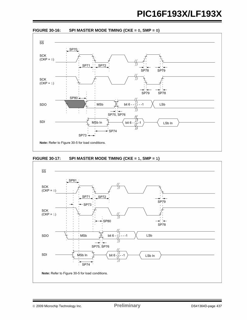
PIC16F193X/LF193X
FIGURE 30-16: SPI MASTER MODE TIMING (CKE = 0, SMP = 0)
FIGURE 30-17: SPI MASTER MODE TIMING (CKE = 1, SMP = 1)
SS
SCK(CKP = 0)
SCK(CKP = 1)
SDO
SDI
SP70
SP71 SP72
SP73SP74
SP75, SP76
SP78SP79
SP80
SP79SP78
MSb LSbbit 6 - - - - - -1
MSb In LSb Inbit 6 - - - -1
Note: Refer to Figure 30-5 for load conditions.
SS
SCK(CKP = 0)
SCK(CKP = 1)
SDO
SDI
SP81
SP71 SP72
SP74
SP75, SP76
SP78SP80
MSb
SP79SP73
MSb In
bit 6 - - - - - -1
LSb Inbit 6 - - - -1
LSb
Note: Refer to Figure 30-5 for load conditions.
2009 Microchip Technology Inc. Preliminary DS41364D-page 437

PIC16F193X/LF193X
FIGURE 30-18: SPI SLAVE MODE TIMING (CKE = 0)
FIGURE 30-19: SPI SLAVE MODE TIMING (CKE = 1)
SS
SCK(CKP = 0)
SCK(CKP = 1)
SDO
SDI
SP70
SP71 SP72
SP73
SP74
SP75, SP76 SP77
SP78SP79
SP80
SP79SP78
MSb LSbbit 6 - - - - - -1
MSb In bit 6 - - - -1 LSb In
SP83
Note: Refer to Figure 30-5 for load conditions.
SS
SCK(CKP = 0)
SCK(CKP = 1)
SDO
SDI
SP70
SP71 SP72
SP82
SP74
SP75, SP76
MSb bit 6 - - - - - -1 LSb
SP77
MSb In bit 6 - - - -1 LSb In
SP80
SP83
Note: Refer to Figure 30-5 for load conditions.
DS41364D-page 438 Preliminary 2009 Microchip Technology Inc.

PIC16F193X/LF193X
TABLE 30-14: SPI MODE REQUIREMENTS
FIGURE 30-20: I2C™ BUS START/STOP BITS TIMING
Param No.
Symbol Characteristic Min. Typ† Max. Units Conditions
SP70* TSSL2SCH, TSSL2SCL
SS to SCK or SCK input TCY — — ns
SP71* TSCH SCK input high time (Slave mode) TCY + 20 — — ns
SP72* TSCL SCK input low time (Slave mode) TCY + 20 — — ns
SP73* TDIV2SCH, TDIV2SCL
Setup time of SDI data input to SCK edge 100 — — ns
SP74* TSCH2DIL, TSCL2DIL
Hold time of SDI data input to SCK edge 100 — — ns
SP75* TDOR SDO data output rise time 3.0-5.5V — 10 25 ns
1.8-5.5V — 25 50 ns
SP76* TDOF SDO data output fall time — 10 25 ns
SP77* TSSH2DOZ SS to SDO output high-impedance 10 — 50 ns
SP78* TSCR SCK output rise time (Master mode)
3.0-5.5V — 10 25 ns
1.8-5.5V — 25 50 ns
SP79* TSCF SCK output fall time (Master mode) — 10 25 ns
SP80* TSCH2DOV,TSCL2DOV
SDO data output valid after SCK edge
3.0-5.5V — — 50 ns
1.8-5.5V — — 145 ns
SP81* TDOV2SCH,TDOV2SCL
SDO data output setup to SCK edge Tcy — — ns
SP82* TSSL2DOV SDO data output valid after SS edge — — 50 ns
SP83* TSCH2SSH,TSCL2SSH
SS after SCK edge 1.5TCY + 40 — — ns
* These parameters are characterized but not tested.
† Data in “Typ” column is at 3.0V, 25°C unless otherwise stated. These parameters are for design guidance only and are not tested.
Note: Refer to Figure 30-5 for load conditions.
SP91
SP92
SP93SCL
SDA
StartCondition
StopCondition
SP90
2009 Microchip Technology Inc. Preliminary DS41364D-page 439

PIC16F193X/LF193X
TABLE 30-15: I2C™ BUS START/STOP BITS REQUIREMENTS
FIGURE 30-21: I2C™ BUS DATA TIMING
ParamNo.
Symbol Characteristic Min. Typ Max. Units Conditions
SP90* TSU:STA Start condition 100 kHz mode 4700 — — ns Only relevant for Repeated Start conditionSetup time 400 kHz mode 600 — —
SP91* THD:STA Start condition 100 kHz mode 4000 — — ns After this period, the first clock pulse is generatedHold time 400 kHz mode 600 — —
SP92* TSU:STO Stop condition 100 kHz mode 4700 — — ns
Setup time 400 kHz mode 600 — —
SP93 THD:STO Stop condition 100 kHz mode 4000 — — ns
Hold time 400 kHz mode 600 — —
* These parameters are characterized but not tested.
Note: Refer to Figure 30-5 for load conditions.
SP90
SP91 SP92
SP100SP101
SP103
SP106SP107
SP109SP109
SP110
SP102
SCL
SDAIn
SDAOut
DS41364D-page 440 Preliminary 2009 Microchip Technology Inc.

PIC16F193X/LF193X
TABLE 30-16: I2C™ BUS DATA REQUIREMENTS
Param.No.
Symbol Characteristic Min. Max. Units Conditions
SP100* THIGH Clock high time 100 kHz mode 4.0 — s Device must operate at a minimum of 1.5 MHz
400 kHz mode 0.6 — s Device must operate at a minimum of 10 MHz
SSP module 1.5TCY —
SP101* TLOW Clock low time 100 kHz mode 4.7 — s Device must operate at a minimum of 1.5 MHz
400 kHz mode 1.3 — s Device must operate at a minimum of 10 MHz
SSP module 1.5TCY —
SP102* TR SDA and SCL rise time
100 kHz mode — 1000 ns
400 kHz mode 20 + 0.1CB 300 ns CB is specified to be from 10-400 pF
SP103* TF SDA and SCL fall time
100 kHz mode — 250 ns
400 kHz mode 20 + 0.1CB 250 ns CB is specified to be from 10-400 pF
SP106* THD:DAT Data input hold time 100 kHz mode 0 — ns
400 kHz mode 0 0.9 s
SP107* TSU:DAT Data input setup time
100 kHz mode 250 — ns (Note 2)
400 kHz mode 100 — ns
SP109* TAA Output valid from clock
100 kHz mode — 3500 ns (Note 1)
400 kHz mode — — ns
SP110* TBUF Bus free time 100 kHz mode 4.7 — s Time the bus must be free before a new transmission can start
400 kHz mode 1.3 — s
SP111 CB Bus capacitive loading — 400 pF
* These parameters are characterized but not tested.
Note 1: As a transmitter, the device must provide this internal minimum delay time to bridge the undefined region (min. 300 ns) of the falling edge of SCL to avoid unintended generation of Start or Stop conditions.
2: A Fast mode (400 kHz) I2C™ bus device can be used in a Standard mode (100 kHz) I2C bus system, but the requirement TSU:DAT 250 ns must then be met. This will automatically be the case if the device does not stretch the low period of the SCL signal. If such a device does stretch the low period of the SCL signal, it must output the next data bit to the SDA line TR max. + TSU:DAT = 1000 + 250 = 1250 ns (according to the Standard mode I2C bus specification), before the SCL line is released.
2009 Microchip Technology Inc. Preliminary DS41364D-page 441

PIC16F193X/LF193X
TABLE 30-17: CAP SENSE OSCILLATOR SPECIFICATIONS
FIGURE 30-22: CAP SENSE OSCILLATOR
Param.No.
Symbol Characteristic Min. Typ† Max. Units Conditions
CS01 ISRC Current Source High -3 -8 -15 A
Medium -0.8 -1.5 -3 A
Low -0.1 -0.3 -0.4 A
CS02 ISNK Current Sink High 2.5 7.5 14 A
Medium 0.6 1.5 2.9 A
Low 0.1 0.25 0.6 A
CS03 VCTH Cap Threshold — 0.8 — mV
CS04 VCTL Cap Threshold — 0.4 — mV
CS05 VCHYST Cap Hysteresis (VCTH-VCTL)
HighMediumLow
350250175
525375300
725500\425
mVmVmV
* These parameters are characterized but not tested.
† Data in “Typ” column is at 3.0V, 25°C unless otherwise stated. These parameters are for design guidance only and are not tested.
ISRC
VCTH
VCTL
ISNKEnabledEnabled
DS41364D-page 442 Preliminary 2009 Microchip Technology Inc.

PIC16F193X/LF193X
31.0 ELECTRICAL SPECIFICATIONS (PIC16F/LF1938/39)
Absolute Maximum Ratings(†)
Ambient temperature under bias....................................................................................................... -40°C to +125°C
Storage temperature ........................................................................................................................ -65°C to +150°C
Voltage on VDD with respect to VSS, PIC16F1938/39 ........................................................................ -0.3V to +6.5V
Voltage on VCAP pin with respect to VSS, PIC16F1938/39 .................................................................. -0.3V to +4.0V
Voltage on VDD with respect to VSS, PIC16LF1938/39 ...................................................................... -0.3V to +4.0V
Voltage on MCLR with respect to Vss ................................................................................................. -0.3V to +9.0V
Voltage on all other pins with respect to VSS ........................................................................... -0.3V to (VDD + 0.3V)
Total power dissipation(1) ............................................................................................................................... 800 mW
Maximum current out of VSS pin, -40°C TA +85°C for industrial............................................................... 340 mA
Maximum current out of VSS pin, -40°C TA +125°C for extended ........................................................... 140 mA
Maximum current into VDD pin, -40°C TA +85°C for industrial.................................................................. 255 mA
Maximum current into VDD pin, -40°C TA +125°C for extended .............................................................. 105 mA
Clamp current, IK (VPIN < 0 or VPIN > VDD)20 mA
Maximum output current sunk by any I/O pin.................................................................................................... 25 mA
Maximum output current sourced by any I/O pin .............................................................................................. 25 mA
Note 1: Power dissipation is calculated as follows: PDIS = VDD x {IDD – IOH} + {(VDD – VOH) x IOH} + (VOl x IOL).
† NOTICE: Stresses above those listed under “Absolute Maximum Ratings” may cause permanent damage to the device. This is a stress rating only and functional operation of the device at those or any other conditions above those indicated in the operation listings of this specification is not implied. Exposure above maximum rating conditions for extended periods may affect device reliability.
2009 Microchip Technology Inc. Preliminary DS41364D-page 443

PIC16F193X/LF193X
FIGURE 31-1: PIC16F/LF1938/39 VOLTAGE FREQUENCY GRAPH, -40°C TA +125°C
FIGURE 31-2: PIC16F/LF1938/39 VOLTAGE FREQUENCY GRAPH, -40°C TA +125°C
1.8
2.5
2.0
0
2.3
Frequency (MHz)
VD
D (
V)
Note 1: The shaded region indicates the permissible combinations of voltage and frequency.2: Refer to Table 31-1 for each Oscillator mode’s supported frequencies.
4 3210 16
5.5
3.6
1.8
2.5
2.0
0
2.3
Frequency (MHz)
VD
D (
V)
Note 1: The shaded region indicates the permissible combinations of voltage and frequency.2: Refer to Table 31-1 for each Oscillator mode’s supported frequencies.
4 3210 16
3.6
DS41364D-page 444 Preliminary 2009 Microchip Technology Inc.
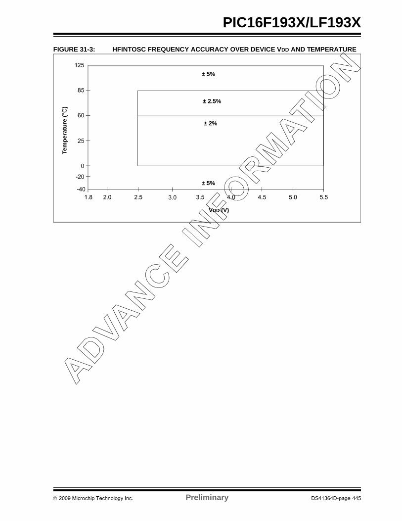
PIC16F193X/LF193X
FIGURE 31-3: HFINTOSC FREQUENCY ACCURACY OVER DEVICE VDD AND TEMPERATURE
125
25
2.0
0
60
85
VDD (V)
4.0 5.04.5
Tem
pe
ratu
re (
°C)
2.5 3.0 3.5 5.51.8-40
-20
± 5%
± 2%
± 5%
± 2.5%
2009 Microchip Technology Inc. Preliminary DS41364D-page 445

PIC16F193X/LF193X
31.1 DC Characteristics: PIC16F/LF1938/39-I/E (Industrial, Extended)
PIC16LF1938/39Standard Operating Conditions (unless otherwise stated)Operating temperature -40°C TA +85°C for industrial
-40°C TA +125°C for extended
PIC16F1938/39Standard Operating Conditions (unless otherwise stated)Operating temperature -40°C TA +85°C for industrial
-40°C TA +125°C for extended
Param. No.
Sym. Characteristic Min. Typ† Max. Units Conditions
D001 VDD Supply Voltage
PIC16LF1938/39 1.82.3
——
3.63.6
VV
FOSC 16 MHz:FOSC 32 MHz (NOTE 2)
D001 PIC16F1938/39 1.82.3
——
5.55.5
VV
FOSC 16 MHz:FOSC 32 MHz (NOTE 2)
D002* VDR RAM Data Retention Voltage(1)
PIC16LF1938/39 1.5 — — V Device in Sleep mode
D002* PIC16F1938/39 1.7 — — V Device in Sleep mode
VPOR* Power-on Reset Release Voltage — 1.6 — V
VPORR* Power-on Reset Rearm Voltage
PIC16LF1938/39 — 0.8 — V Device in Sleep mode
PIC16F1938/39 — 1.7 — V Device in Sleep mode
D003 VADFVR Fixed Voltage Reference Voltage for ADC, Initial Accuracy
-6-7-7-8-7-8
——————
446644
% 1.024V, VDD 1.8V, 85°C1.024V, VDD 1.8V, 125°C2.048V, VDD 2.5V, 85°C2.048V, VDD 2.5V, 125°C4.096V, VDD 4.75V, 85°C4.096V, VDD 4.75V, 125°C
D003A VCDAFVR Fixed Voltage Reference Voltage for Comparator and DAC, Initial Accuracy
-7-8-8-9-8-8
——————
557744
% 1.024V, VDD 1.8V, 85°C1.024V, VDD 1.8V, 125°C2.048V, VDD 2.5V, 85°C2.048V, VDD 2.5V, 125°C4.096V, VDD 4.75V, 85°C4.096V, VDD 4.75V, 125°C
D003B VLCDFVR Fixed Voltage Reference Voltage for LCD Bias, Initial Accuracy
-9-9.5
——
99
% 3.072V, VDD 3.6V, 85°C3.072V, VDD 3.6V, 125°C
D003C* TCVFVR Temperature Coefficient, Fixed Voltage Reference
— -130 — ppm/°C
D003D* VFVR/VIN
Line Regulation, Fixed Voltage Ref-erence
— 0.270 — %/V
D004* SVDD VDD Rise Rate to ensure internal Power-on Reset signal
0.05 — — V/ms See Section 6.1 “Power-on Reset (POR)” for details.
* These parameters are characterized but not tested.† Data in “Typ” column is at 3.3V, 25°C unless otherwise stated. These parameters are for design guidance only and are not
tested.
Note 1: This is the limit to which VDD can be lowered in Sleep mode without losing RAM data.2: PLL required for 32 MHz operation.
DS41364D-page 446 Preliminary 2009 Microchip Technology Inc.
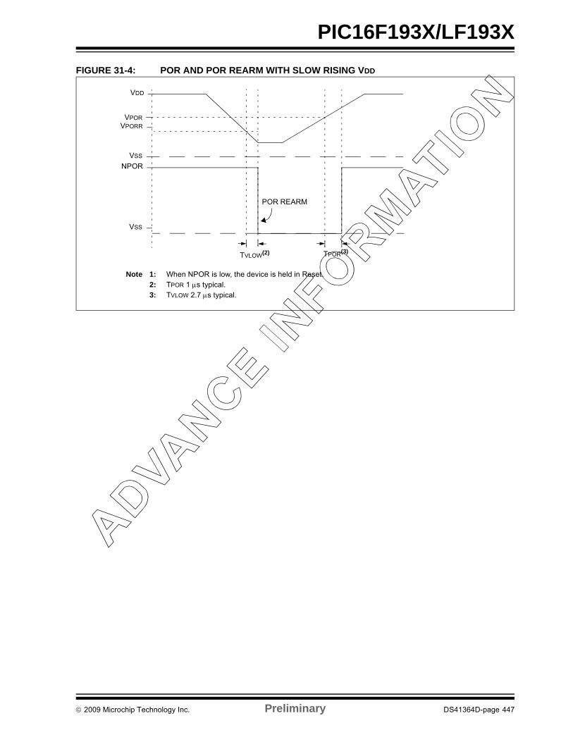
PIC16F193X/LF193X
FIGURE 31-4: POR AND POR REARM WITH SLOW RISING VDD
VDD
VPOR
VPORR
VSS
VSS
NPOR
TPOR(3)
POR REARM
Note 1: When NPOR is low, the device is held in Reset.2: TPOR 1 s typical.3: TVLOW 2.7 s typical.
TVLOW(2)
2009 Microchip Technology Inc. Preliminary DS41364D-page 447

PIC16F193X/LF193X
31.2 DC Characteristics: PIC16F/LF1938/39-I/E (Industrial, Extended)
PIC16LF1938/39Standard Operating Conditions (unless otherwise stated)Operating temperature -40°C TA +85°C for industrial
-40°C TA +125°C for extended
PIC16F1938/39Standard Operating Conditions (unless otherwise stated)Operating temperature -40°C TA +85°C for industrial
-40°C TA +125°C for extended
ParamNo.
Device Characteristics
Min. Typ† Max. UnitsConditions
VDD Note
Supply Current (IDD)(1, 2)
D009 LDO Regulator — 350 — A — HS, EC OR INTOSC/INTOSCIO (8-16 MHZ) Clock modes with all VCAP pins disabled
— 50 — A — All VCAP pins disabled
— 30 — A — VCAP enabled on RA0, RA5 or RA6
— 5 — A — LP Clock mode and Sleep (requires FVR and BOR to be disabled)
D010 — 7.0 16 A 1.8 FOSC = 32 kHzLP Oscillator mode (Note 4),-40°C TA +85°C
— 9.0 20 A 3.0
D010 — 24 40 A 1.8 FOSC = 32 kHzLP Oscillator mode (Note 4, 5),-40°C TA +85°C
— 30 45 A 3.0
— 32 50 A 5.0
D010A — 7.0 — A 1.8 FOSC = 32 kHzLP Oscillator mode (Note 4)-40°C TA +125°C
— 9.0 — A 3.0
D010A — 24 — A 1.8 FOSC = 32 kHzLP Oscillator mode (Note 4, 5)-40°C TA +125°C
— 30 — A 3.0
— 32 — A 5.0
D011 — 150 200 A 1.8 FOSC = 1 MHzXT Oscillator mode— 270 325 A 3.0
D011 — 160 255 A 1.8 FOSC = 1 MHzXT Oscillator mode (Note 5)— 280 475 A 3.0
— 390 690 A 5.0
D012 — 430 495 A 1.8 FOSC = 4 MHzXT Oscillator mode— 750 1000 A 3.0
D012 — 450 645 A 1.8 FOSC = 4 MHzXT Oscillator mode (Note 5)— 770 1100 A 3.0
— 930 1320 A 5.0
Note 1: The test conditions for all IDD measurements in active operation mode are: OSC1 = external square wave, from rail-to-rail; all I/O pins tri-stated, pulled to VDD; MCLR = VDD; WDT disabled.
2: The supply current is mainly a function of the operating voltage and frequency. Other factors, such as I/O pin loading and switching rate, oscillator type, internal code execution pattern and temperature, also have an impact on the current consumption.
3: For RC oscillator configurations, current through REXT is not included. The current through the resistor can be extended by the formula IR = VDD/2REXT (mA) with REXT in k
4: FVR and BOR are disabled.5: 0.1 F capacitor on VCAP (RA0).6: 8 MHz crystal oscillator with 4x PLL enabled.
DS41364D-page 448 Preliminary 2009 Microchip Technology Inc.

PIC16F193X/LF193X
Supply Current (IDD)(1, 2)
D013 — 90 125 A 1.8 FOSC = 500 kHzEC Oscillator Low-Power mode— 170 200 A 3.0
D013 — 100 180 A 1.8 FOSC = 500 kHzEC Oscillator Low-Power mode (Note 5)— 180 310 A 3.0
— 225 350 A 5.0
D014 — 450 650 A 1.8 FOSC = 4 MHzEC Oscillator modeMedium Power mode
— 830 1100 A 3.0
D014 — 475 735 A 1.8 FOSC = 4 MHzEC Oscillator mode (Note 5)Medium Power mode
— 850 1200 A 3.0
— 980 1390 A 5.0
D015 — 5.3 7.3 mA 3.0 FOSC = 32 MHzEC Oscillator High-Power mode— 6.0 8.0 mA 3.6
D015 — 5.3 7.3 mA 3.0 FOSC = 32 MHzEC Oscillator High-Power mode (Note 5)— 6.0 8.0 mA 5.0
D016 — 5 12 A 1.8 FOSC = 32 kHzLFINTOSC mode, 85°C— 8 16 A 3.0
D016 — 21 35 A 1.8 FOSC = 32 kHzLFINTOSC mode, 85°C (Note 5)— 27 40 A 3.0
— 28 45 A 5.0
31.2 DC Characteristics: PIC16F/LF1938/39-I/E (Industrial, Extended) (Continued)
PIC16LF1938/39Standard Operating Conditions (unless otherwise stated)Operating temperature -40°C TA +85°C for industrial
-40°C TA +125°C for extended
PIC16F1938/39Standard Operating Conditions (unless otherwise stated)Operating temperature -40°C TA +85°C for industrial
-40°C TA +125°C for extended
ParamNo.
Device Characteristics
Min. Typ† Max. UnitsConditions
VDD Note
Note 1: The test conditions for all IDD measurements in active operation mode are: OSC1 = external square wave, from rail-to-rail; all I/O pins tri-stated, pulled to VDD; MCLR = VDD; WDT disabled.
2: The supply current is mainly a function of the operating voltage and frequency. Other factors, such as I/O pin loading and switching rate, oscillator type, internal code execution pattern and temperature, also have an impact on the current consumption.
3: For RC oscillator configurations, current through REXT is not included. The current through the resistor can be extended by the formula IR = VDD/2REXT (mA) with REXT in k
4: FVR and BOR are disabled.5: 0.1 F capacitor on VCAP (RA0).6: 8 MHz crystal oscillator with 4x PLL enabled.
2009 Microchip Technology Inc. Preliminary DS41364D-page 449
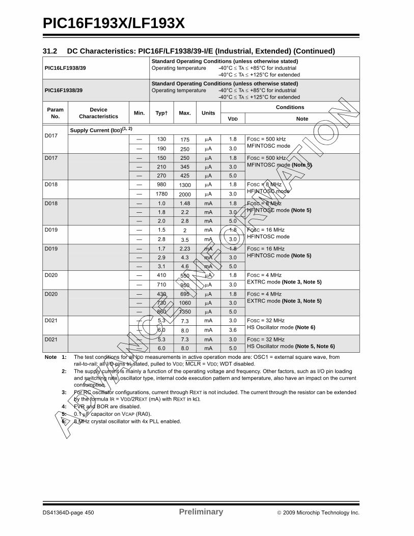
PIC16F193X/LF193X
D017Supply Current (IDD)(1, 2)
— 130 175 A 1.8 FOSC = 500 kHzMFINTOSC mode— 190 250 A 3.0
D017 — 150 250 A 1.8 FOSC = 500 kHzMFINTOSC mode (Note 5)— 210 345 A 3.0
— 270 425 A 5.0
D018 — 980 1300 A 1.8 FOSC = 8 MHzHFINTOSC mode— 1780 2000 A 3.0
D018 — 1.0 1.48 mA 1.8 FOSC = 8 MHzHFINTOSC mode (Note 5)— 1.8 2.2 mA 3.0
— 2.0 2.8 mA 5.0
D019 — 1.5 2 mA 1.8 FOSC = 16 MHzHFINTOSC mode— 2.8 3.5 mA 3.0
D019 — 1.7 2.23 mA 1.8 FOSC = 16 MHzHFINTOSC mode (Note 5)— 2.9 4.3 mA 3.0
— 3.1 4.6 mA 5.0
D020 — 410 550 A 1.8 FOSC = 4 MHzEXTRC mode (Note 3, Note 5)— 710 950 A 3.0
D020 — 430 695 A 1.8 FOSC = 4 MHzEXTRC mode (Note 3, Note 5)— 730 1060 A 3.0
— 860 1350 A 5.0
D021 — 5.3 7.3 mA 3.0 FOSC = 32 MHzHS Oscillator mode (Note 6)— 6.0 8.0 mA 3.6
D021 — 5.3 7.3 mA 3.0 FOSC = 32 MHzHS Oscillator mode (Note 5, Note 6)— 6.0 8.0 mA 5.0
31.2 DC Characteristics: PIC16F/LF1938/39-I/E (Industrial, Extended) (Continued)
PIC16LF1938/39Standard Operating Conditions (unless otherwise stated)Operating temperature -40°C TA +85°C for industrial
-40°C TA +125°C for extended
PIC16F1938/39Standard Operating Conditions (unless otherwise stated)Operating temperature -40°C TA +85°C for industrial
-40°C TA +125°C for extended
ParamNo.
Device Characteristics
Min. Typ† Max. UnitsConditions
VDD Note
Note 1: The test conditions for all IDD measurements in active operation mode are: OSC1 = external square wave, from rail-to-rail; all I/O pins tri-stated, pulled to VDD; MCLR = VDD; WDT disabled.
2: The supply current is mainly a function of the operating voltage and frequency. Other factors, such as I/O pin loading and switching rate, oscillator type, internal code execution pattern and temperature, also have an impact on the current consumption.
3: For RC oscillator configurations, current through REXT is not included. The current through the resistor can be extended by the formula IR = VDD/2REXT (mA) with REXT in k
4: FVR and BOR are disabled.5: 0.1 F capacitor on VCAP (RA0).6: 8 MHz crystal oscillator with 4x PLL enabled.
DS41364D-page 450 Preliminary 2009 Microchip Technology Inc.

PIC16F193X/LF193X
31.3 DC Characteristics: PIC16F/LF1938/39-I/E (Power-Down)
PIC16LF1938/39Standard Operating Conditions (unless otherwise stated)Operating temperature -40°C TA +85°C for industrial
-40°C TA +125°C for extended
PIC16F1938/39Standard Operating Conditions (unless otherwise stated)Operating temperature -40°C TA +85°C for industrial
-40°C TA +125°C for extended
ParamNo.
Device Characteristics Min. Typ†Max.
+85°CMax.
+125°CUnits
Conditions
VDD Note
Power-down Base Current (IPD)(2)
D023 — 0.06 1 — A 1.8 WDT, BOR, FVR, and T1OSC disabled, all Peripherals Inactive— 0.08 2 — A 3.0
D023 — 15 35 — A 1.8 WDT, BOR, FVR, and T1OSC disabled, all Peripherals Inactive— 18 40 — A 3.0
— 19 45 — A 5.0
D024 — 0.5 6 — A 1.8 LPWDT Current (Note 1)
— 0.8 7 — A 3.0
D024 — 16 35 — A 1.8 LPWDT Current (Note 1)
— 19 40 — A 3.0
— 20 45 — A 5.0
D025 — 8.5 23 — A 1.8 FVR current
— 8.5 26 — A 3.0
D025 — 32 50 — A 1.8 FVR current (Note 4)
— 39 72 — A 3.0
— 70 120 — A 5.0
D026 — 7.5 TBD — A 3.0 BOR Current (Note 1)
D026 — 34 57 — A 3.0 BOR Current (Note 1, Note 4)
— 67 100 — A 5.0
D027 — 0.6 5 — A 1.8 T1OSC Current (Note 1)
— 1.8 6 — A 3.0
D027 — 16 35 — A 1.8 T1OSC Current (Note 1)
— 21 40 — A 3.0
— 25 45 — A 5.0
* These parameters are characterized but not tested.† Data in “Typ” column is at 3.0V, 25°C unless otherwise stated. These parameters are for design guidance only and are
not tested.Legend: TBD = To Be DeterminedNote 1: The peripheral current is the sum of the base IDD or IPD and the additional current consumed when this peripheral is
enabled. The peripheral current can be determined by subtracting the base IDD or IPD current from this limit. Max values should be used when calculating total current consumption.
2: The power-down current in Sleep mode does not depend on the oscillator type. Power-down current is measured with the part in Sleep mode, with all I/O pins in high-impedance state and tied to VDD.
3: A/D oscillator source is FRC.4: 0.1 F capacitor on VCAP (RA0).
2009 Microchip Technology Inc. Preliminary DS41364D-page 451
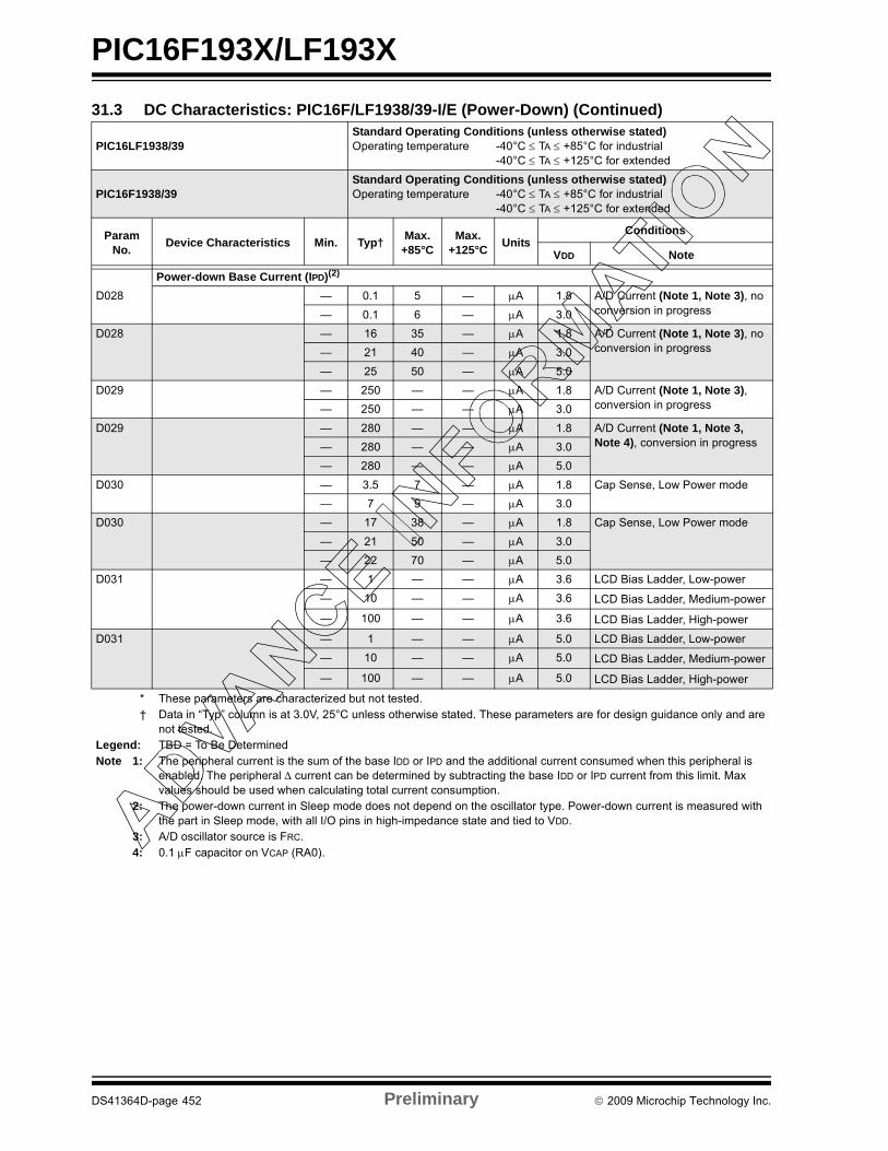
PIC16F193X/LF193X
Power-down Base Current (IPD)(2)
D028 — 0.1 5 — A 1.8 A/D Current (Note 1, Note 3), no conversion in progress— 0.1 6 — A 3.0
D028 — 16 35 — A 1.8 A/D Current (Note 1, Note 3), no conversion in progress— 21 40 — A 3.0
— 25 50 — A 5.0
D029 — 250 — — A 1.8 A/D Current (Note 1, Note 3), conversion in progress— 250 — — A 3.0
D029 — 280 — — A 1.8 A/D Current (Note 1, Note 3, Note 4), conversion in progress— 280 — — A 3.0
— 280 — — A 5.0
D030 — 3.5 7 — A 1.8 Cap Sense, Low Power mode
— 7 9 — A 3.0
D030 — 17 38 — A 1.8 Cap Sense, Low Power mode
— 21 50 — A 3.0
— 22 70 — A 5.0
D031 — 1 — — A 3.6 LCD Bias Ladder, Low-power
— 10 — — A 3.6 LCD Bias Ladder, Medium-power
— 100 — — A 3.6 LCD Bias Ladder, High-power
D031 — 1 — — A 5.0 LCD Bias Ladder, Low-power
— 10 — — A 5.0 LCD Bias Ladder, Medium-power
— 100 — — A 5.0 LCD Bias Ladder, High-power
31.3 DC Characteristics: PIC16F/LF1938/39-I/E (Power-Down) (Continued)
PIC16LF1938/39Standard Operating Conditions (unless otherwise stated)Operating temperature -40°C TA +85°C for industrial
-40°C TA +125°C for extended
PIC16F1938/39Standard Operating Conditions (unless otherwise stated)Operating temperature -40°C TA +85°C for industrial
-40°C TA +125°C for extended
ParamNo.
Device Characteristics Min. Typ†Max.
+85°CMax.
+125°CUnits
Conditions
VDD Note
* These parameters are characterized but not tested.† Data in “Typ” column is at 3.0V, 25°C unless otherwise stated. These parameters are for design guidance only and are
not tested.Legend: TBD = To Be DeterminedNote 1: The peripheral current is the sum of the base IDD or IPD and the additional current consumed when this peripheral is
enabled. The peripheral current can be determined by subtracting the base IDD or IPD current from this limit. Max values should be used when calculating total current consumption.
2: The power-down current in Sleep mode does not depend on the oscillator type. Power-down current is measured with the part in Sleep mode, with all I/O pins in high-impedance state and tied to VDD.
3: A/D oscillator source is FRC.4: 0.1 F capacitor on VCAP (RA0).
DS41364D-page 452 Preliminary 2009 Microchip Technology Inc.
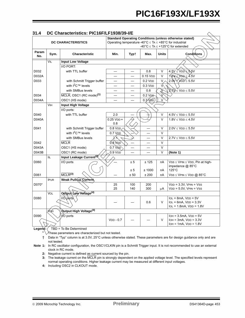
PIC16F193X/LF193X
31.4 DC Characteristics: PIC16F/LF1938/39-I/E
DC CHARACTERISTICSStandard Operating Conditions (unless otherwise stated)Operating temperature -40°C TA +85°C for industrial
-40°C TA +125°C for extended
ParamNo.
Sym. Characteristic Min. Typ† Max. Units Conditions
VIL Input Low Voltage
I/O PORT:
D032 with TTL buffer — — 0.8 V 4.5V VDD 5.5V
D032A — — 0.15 VDD V 1.8V VDD 4.5V
D033 with Schmitt Trigger buffer — — 0.2 VDD V 2.0V VDD 5.5V
with I2C™ levels — — 0.3 VDD V
with SMBus levels — — 0.8 V 2.7V VDD 5.5V
D034 MCLR, OSC1 (RC mode)(1) — — 0.2 VDD V
D034A OSC1 (HS mode) — — 0.3 VDD V
VIH Input High Voltage
I/O ports:
D040 with TTL buffer 2.0 — — V 4.5V VDD 5.5V
D040A 0.25 VDD + 0.8
— — V 1.8V VDD 4.5V
D041 with Schmitt Trigger buffer 0.8 VDD — — V 2.0V VDD 5.5V
with I2C™ levels 0.7 VDD — — V
with SMBus levels 2.1 — — V 2.7V VDD 5.5V
D042 MCLR 0.8 VDD — — V
D043A OSC1 (HS mode) 0.7 VDD — — V
D043B OSC1 (RC mode) 0.9 VDD — — V (Note 1)
IIL Input Leakage Current(2)
D060 I/O ports — ± 5
± 5
± 125
± 1000
nA
nA
VSS VPIN VDD, Pin at high-impedance @ 85°C125°C
D061 MCLR(3) — ± 50 ± 200 nA VSS VPIN VDD @ 85°C
IPUR Weak Pull-up Current
D070* 2525
100140
200300 A
VDD = 3.3V, VPIN = VSS
VDD = 5.0V, VPIN = VSS
VOL Output Low Voltage(4)
D080 I/O ports— — 0.6 V
IOL = 8mA, VDD = 5VIOL = 6mA, VDD = 3.3VIOL = 1.8mA, VDD = 1.8V
VOH Output High Voltage(4)
D090 I/O portsVDD - 0.7 — — V
IOH = 3.5mA, VDD = 5VIOH = 3mA, VDD = 3.3VIOH = 1mA, VDD = 1.8V
Legend: TBD = To Be Determined* These parameters are characterized but not tested.† Data in “Typ” column is at 3.0V, 25°C unless otherwise stated. These parameters are for design guidance only and are
not tested.Note 1: In RC oscillator configuration, the OSC1/CLKIN pin is a Schmitt Trigger input. It is not recommended to use an external
clock in RC mode.2: Negative current is defined as current sourced by the pin.3: The leakage current on the MCLR pin is strongly dependent on the applied voltage level. The specified levels represent
normal operating conditions. Higher leakage current may be measured at different input voltages.4: Including OSC2 in CLKOUT mode.
2009 Microchip Technology Inc. Preliminary DS41364D-page 453
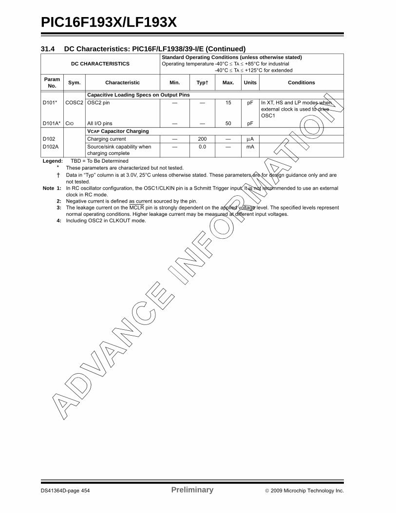
PIC16F193X/LF193X
Capacitive Loading Specs on Output Pins
D101* COSC2 OSC2 pin — — 15 pF In XT, HS and LP modes when external clock is used to drive OSC1
D101A* CIO All I/O pins — — 50 pF
VCAP Capacitor Charging
D102 Charging current — 200 — A
D102A Source/sink capability when charging complete
— 0.0 — mA
31.4 DC Characteristics: PIC16F/LF1938/39-I/E (Continued)
DC CHARACTERISTICSStandard Operating Conditions (unless otherwise stated)Operating temperature -40°C TA +85°C for industrial
-40°C TA +125°C for extended
ParamNo.
Sym. Characteristic Min. Typ† Max. Units Conditions
Legend: TBD = To Be Determined* These parameters are characterized but not tested.† Data in “Typ” column is at 3.0V, 25°C unless otherwise stated. These parameters are for design guidance only and are
not tested.Note 1: In RC oscillator configuration, the OSC1/CLKIN pin is a Schmitt Trigger input. It is not recommended to use an external
clock in RC mode.2: Negative current is defined as current sourced by the pin.3: The leakage current on the MCLR pin is strongly dependent on the applied voltage level. The specified levels represent
normal operating conditions. Higher leakage current may be measured at different input voltages.4: Including OSC2 in CLKOUT mode.
DS41364D-page 454 Preliminary 2009 Microchip Technology Inc.
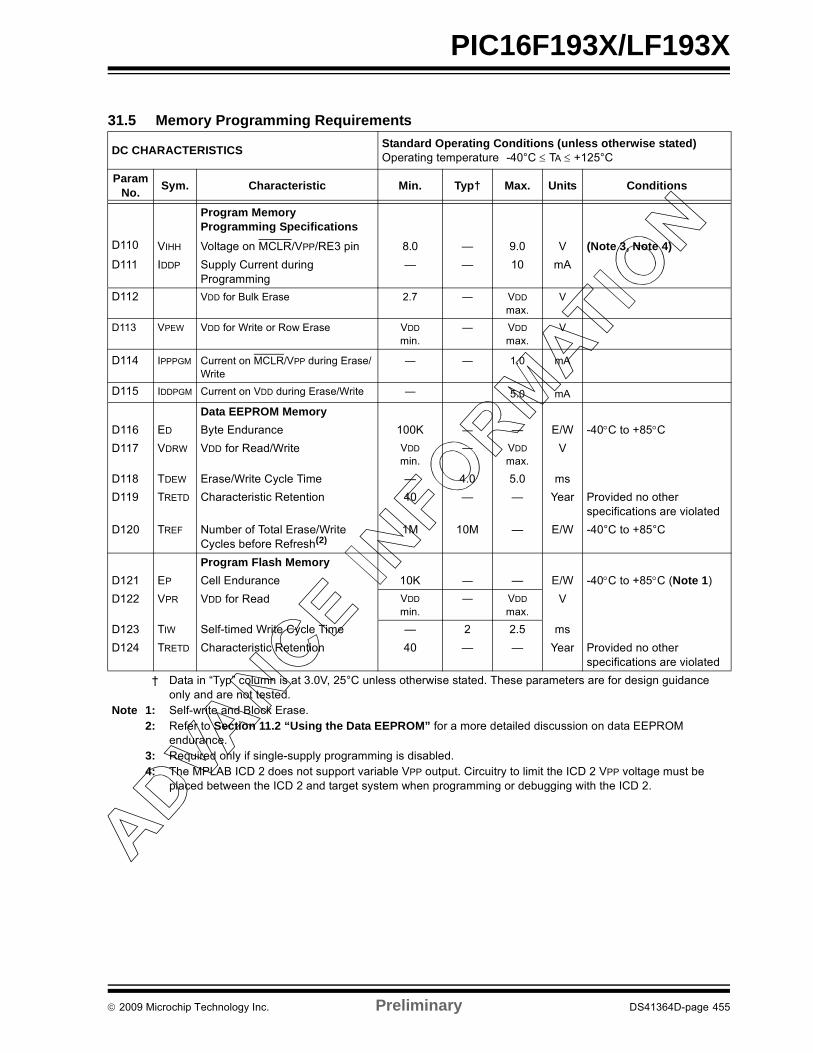
PIC16F193X/LF193X
31.5 Memory Programming Requirements
DC CHARACTERISTICSStandard Operating Conditions (unless otherwise stated)Operating temperature -40°C TA +125°C
ParamNo.
Sym. Characteristic Min. Typ† Max. Units Conditions
Program Memory Programming Specifications
D110 VIHH Voltage on MCLR/VPP/RE3 pin 8.0 — 9.0 V (Note 3, Note 4)
D111 IDDP Supply Current during Programming
— — 10 mA
D112 VDD for Bulk Erase 2.7 — VDD
max.V
D113 VPEW VDD for Write or Row Erase VDD
min.— VDD
max.V
D114 IPPPGM Current on MCLR/VPP during Erase/Write
— — 1.0 mA
D115 IDDPGM Current on VDD during Erase/Write — 5.0 mA
Data EEPROM Memory
D116 ED Byte Endurance 100K — — E/W -40C to +85C
D117 VDRW VDD for Read/Write VDD
min.— VDD
max.V
D118 TDEW Erase/Write Cycle Time — 4.0 5.0 ms
D119 TRETD Characteristic Retention 40 — — Year Provided no other specifications are violated
D120 TREF Number of Total Erase/Write Cycles before Refresh(2)
1M 10M — E/W -40°C to +85°C
Program Flash Memory
D121 EP Cell Endurance 10K — — E/W -40C to +85C (Note 1)
D122 VPR VDD for Read VDD
min.— VDD
max.V
D123 TIW Self-timed Write Cycle Time — 2 2.5 ms
D124 TRETD Characteristic Retention 40 — — Year Provided no other specifications are violated
† Data in “Typ” column is at 3.0V, 25°C unless otherwise stated. These parameters are for design guidance only and are not tested.
Note 1: Self-write and Block Erase.2: Refer to Section 11.2 “Using the Data EEPROM” for a more detailed discussion on data EEPROM
endurance.3: Required only if single-supply programming is disabled.4: The MPLAB ICD 2 does not support variable VPP output. Circuitry to limit the ICD 2 VPP voltage must be
placed between the ICD 2 and target system when programming or debugging with the ICD 2.
2009 Microchip Technology Inc. Preliminary DS41364D-page 455

PIC16F193X/LF193X
31.6 Thermal Considerations
Standard Operating Conditions (unless otherwise stated)Operating temperature -40°C TA +125°C
ParamNo.
Sym. Characteristic Typ. Units Conditions
TH01 JA Thermal Resistance Junction to Ambient 60 C/W 28-pin SPDIP package
80 C/W 28-pin SOIC package
90 C/W 28-pin SSOP package
27.5 C/W 28-pin UQFN 4x4mm package
27.5 C/W 28-pin QFN 6x6mm package
47.2 C/W 40-pin PDIP package
46 C/W 44-pin TQFP package
24.4 C/W 44-pin QFN 8x8mm package
TH02 JC Thermal Resistance Junction to Case 31.4 C/W 28-pin SPDIP package
24 C/W 28-pin SOIC package
24 C/W 28-pin SSOP package
24 C/W 28-pin UQFN 4x4mm package
24 C/W 28-pin QFN 6x6mm package
24.7 C/W 40-pin PDIP package
14.5 C/W 44-pin TQFP package
20 C/W 44-pin QFN 8x8mm package
TH03 TJMAX Maximum Junction Temperature 150 CTH04 PD Power Dissipation — W PD = PINTERNAL + PI/O
TH05 PINTERNAL Internal Power Dissipation — W PINTERNAL = IDD x VDD(1)
TH06 PI/O I/O Power Dissipation — W PI/O = (IOL * VOL) + (IOH * (VDD - VOH))
TH07 PDER Derated Power — W PDER = PDMAX (TJ - TA)/JA(2)
Note 1: IDD is current to run the chip alone without driving any load on the output pins.2: TA = Ambient Temperature3: TJ = Junction Temperature
DS41364D-page 456 Preliminary 2009 Microchip Technology Inc.
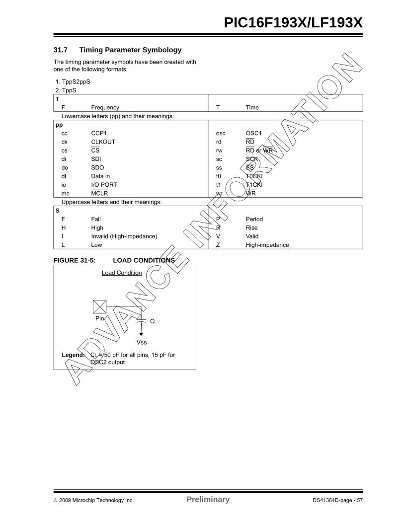
PIC16F193X/LF193X
31.7 Timing Parameter Symbology
The timing parameter symbols have been created withone of the following formats:
FIGURE 31-5: LOAD CONDITIONS
1. TppS2ppS
2. TppS
T
F Frequency T Time
Lowercase letters (pp) and their meanings:
pp
cc CCP1 osc OSC1
ck CLKOUT rd RD
cs CS rw RD or WR
di SDI sc SCK
do SDO ss SS
dt Data in t0 T0CKI
io I/O PORT t1 T1CKI
mc MCLR wr WR
Uppercase letters and their meanings:
S
F Fall P Period
H High R Rise
I Invalid (High-impedance) V Valid
L Low Z High-impedance
VSS
CL
Legend: CL = 50 pF for all pins, 15 pF for OSC2 output
Load Condition
Pin
2009 Microchip Technology Inc. Preliminary DS41364D-page 457

PIC16F193X/LF193X
31.8 AC Characteristics: PIC16F/LF1938/39-I/E
FIGURE 31-6: CLOCK TIMING
TABLE 31-1: CLOCK OSCILLATOR TIMING REQUIREMENTS
OSC1/CLKIN
OSC2/CLKOUT
Q4 Q1 Q2 Q3 Q4 Q1
OS02
OS03OS04 OS04
OSC2/CLKOUT(LP,XT,HS Modes)
(CLKOUT Mode)
Standard Operating Conditions (unless otherwise stated)Operating temperature -40°C TA +125°C
ParamNo.
Sym. Characteristic Min. Typ† Max. Units Conditions
OS01 FOSC External CLKIN Frequency(1) DC — 0.5 MHz EC Oscillator mode (low)
DC — 4 MHz EC Oscillator mode (medium)
DC — 32 MHz EC Oscillator mode (high)
Oscillator Frequency(1) — 32.768 — kHz LP Oscillator mode
0.1 — 4 MHz XT Oscillator mode
1 — 4 MHz HS Oscillator mode, VDD 2.7V
1 — 20 MHz HS Oscillator mode, VDD > 2.7V
DC — 4 MHz RC Oscillator mode
OS02 TOSC External CLKIN Period(1) 27 — s LP Oscillator mode
250 — ns XT Oscillator mode
50 — ns HS Oscillator mode
31.25 — ns EC Oscillator mode
Oscillator Period(1) — 30.5 — s LP Oscillator mode
250 — 10,000 ns XT Oscillator mode
50 — 1,000 ns HS Oscillator mode
250 — — ns RC Oscillator mode
OS03 TCY Instruction Cycle Time(1) 200 TCY DC ns TCY = 4/FOSC
OS04* TosH,TosL
External CLKIN High,External CLKIN Low
2 — — s LP oscillator
100 — — ns XT oscillator
20 — — ns HS oscillator
OS05* TosR,TosF
External CLKIN Rise,External CLKIN Fall
0 — ns LP oscillator
0 — ns XT oscillator
0 — ns HS oscillator
* These parameters are characterized but not tested.† Data in “Typ” column is at 3.0V, 25°C unless otherwise stated. These parameters are for design guidance only and are not
tested.Note 1: Instruction cycle period (TCY) equals four times the input oscillator time base period. All specified values are based on
characterization data for that particular oscillator type under standard operating conditions with the device executing code. Exceeding these specified limits may result in an unstable oscillator operation and/or higher than expected current con-sumption. All devices are tested to operate at “min” values with an external clock applied to OSC1 pin. When an external clock input is used, the “max” cycle time limit is “DC” (no clock) for all devices.
DS41364D-page 458 Preliminary 2009 Microchip Technology Inc.

PIC16F193X/LF193X
TABLE 31-2: OSCILLATOR PARAMETERS
TABLE 31-3: PLL CLOCK TIMING SPECIFICATIONS (VDD = 2.7V TO 5.5V)
Standard Operating Conditions (unless otherwise stated)Operating Temperature -40°C TA +125°C
Param No.
Sym. CharacteristicFreq.
ToleranceMin. Typ† Max. Units Conditions
OS08 HFOSC Internal Calibrated HFINTOSC Frequency(2)
2%2.5%
——
16.016.0
——
MHzMHz
0°C TA +60°C, VDD 2.5V+60°C TA +85°C, VDD 2.5V
5% — 16.0 — MHz -40°C TA +125°C
OS08A MFOSC Internal Calibrated MFINTOSC Frequency(2)
2%2.5%
——
500500
——
kHzkHz
0°C TA +60°C, VDD 2.5V+60°C TA +85°C, VDD 2.5V
5% — 500 — kHz -40°C TA +125°C
OS10* TIOSC ST HFINTOSCWake-up from Sleep Start-up TimeMFINTOSCWake-up from Sleep Start-up Time
— — 5 8 s
— — 20 30 s
* These parameters are characterized but not tested.† Data in “Typ” column is at 3.0V, 25°C unless otherwise stated. These parameters are for design guidance only and are not
tested.Note 1: Instruction cycle period (TCY) equals four times the input oscillator time base period. All specified values are based on char-
acterization data for that particular oscillator type under standard operating conditions with the device executing code. Exceeding these specified limits may result in an unstable oscillator operation and/or higher than expected current con-sumption. All devices are tested to operate at “min” values with an external clock applied to the OSC1 pin. When an exter-nal clock input is used, the “max” cycle time limit is “DC” (no clock) for all devices.
2: To ensure these oscillator frequency tolerances, VDD and VSS must be capacitively decoupled as close to the device as possible. 0.1 F and 0.01 F values in parallel are recommended.
3: By design.
Param No.
Sym. Characteristic Min. Typ† Max. Units Conditions
F10 FOSC Oscillator Frequency Range 4 — 8 MHz
F11 FSYS On-Chip VCO System Frequency 16 — 32 MHz
F12 TRC PLL Start-up Time (Lock Time) — — 2 ms
F13* CLK CLKOUT Stability (Jitter) -0.25% — +0.25% %
* These parameters are characterized but not tested.
† Data in “Typ” column is at 5V, 25C unless otherwise stated. These parameters are for design guidance only and are not tested.
2009 Microchip Technology Inc. Preliminary DS41364D-page 459

PIC16F193X/LF193X
FIGURE 31-7: CLKOUT AND I/O TIMING
FOSC
CLKOUT
I/O pin(Input)
I/O pin(Output)
Q4 Q1 Q2 Q3
OS11
OS19
OS13
OS15
OS18, OS19
OS20OS21
OS17
OS16
OS14
OS12
OS18
Old Value New Value
Write Fetch Read ExecuteCycle
DS41364D-page 460 Preliminary 2009 Microchip Technology Inc.

PIC16F193X/LF193X
TABLE 31-4: CLKOUT AND I/O TIMING PARAMETERS
FIGURE 31-8: RESET, WATCHDOG TIMER, OSCILLATOR START-UP TIMER AND POWER-UP TIMER TIMING
Standard Operating Conditions (unless otherwise stated)Operating Temperature -40°C TA +125°C
Param No.
Sym. Characteristic Min. Typ† Max. Units Conditions
OS11 TosH2ckL FOSC to CLKOUT (1) — — 70 ns VDD = 3.3-5.0V
OS12 TosH2ckH FOSC to CLKOUT (1) — — 72 ns VDD = 3.3-5.0V
OS13 TckL2ioV CLKOUT to Port out valid(1) — — 20 ns
OS14 TioV2ckH Port input valid before CLKOUT(1) TOSC + 200 ns — — ns
OS15 TosH2ioV Fosc (Q1 cycle) to Port out valid — 50 70* ns VDD = 3.3-5.0V
OS16 TosH2ioI Fosc (Q2 cycle) to Port input invalid (I/O in hold time)
50 — — ns VDD = 3.3-5.0V
OS17 TioV2osH Port input valid to Fosc(Q2 cycle)(I/O in setup time)
20 — — ns
OS18 TioR Port output rise time(2) ——
4015
7232
ns VDD = 1.8VVDD = 3.3-5.0V
OS19 TioF Port output fall time(2) ——
2815
5530
ns VDD = 1.8VVDD = 3.3-5.0V
OS20* Tinp INT pin input high or low time 25 — — ns
OS21* Tioc Interrupt-on-change new input level time
25 — — ns
* These parameters are characterized but not tested.† Data in “Typ” column is at 3.0V, 25C unless otherwise stated.
Note 1: Measurements are taken in RC mode where CLKOUT output is 4 x TOSC.2: Includes OSC2 in CLKOUT mode.
VDD
MCLR
InternalPOR
PWRTTime-out
OSCStart-Up Time
Internal Reset(1)
Watchdog Timer
33
32
30
3134
I/O pins
34
Note 1: Asserted low.
Reset(1)
2009 Microchip Technology Inc. Preliminary DS41364D-page 461
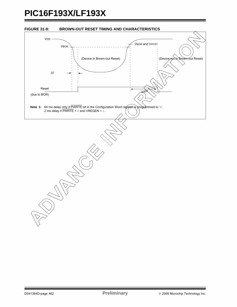
PIC16F193X/LF193X
FIGURE 31-9: BROWN-OUT RESET TIMING AND CHARACTERISTICS
VBOR
VDD
(Device in Brown-out Reset) (Device not in Brown-out Reset)
33(1)
Note 1: 64 ms delay only if PWRTE bit in the Configuration Word register is programmed to ‘0’. 2 ms delay if PWRTE = 0 and VREGEN = 1.
Reset
(due to BOR)
VBOR and VHYST
37
DS41364D-page 462 Preliminary 2009 Microchip Technology Inc.
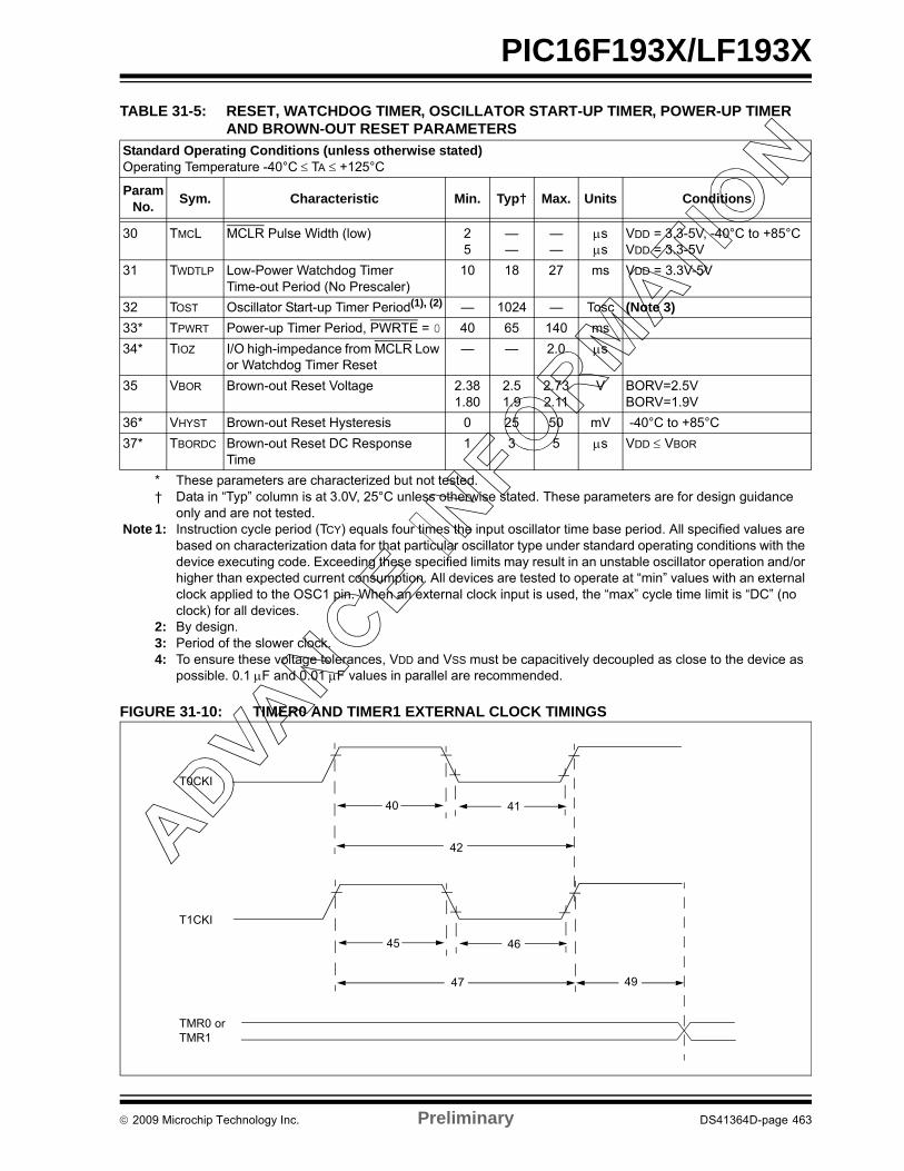
PIC16F193X/LF193X
TABLE 31-5: RESET, WATCHDOG TIMER, OSCILLATOR START-UP TIMER, POWER-UP TIMER AND BROWN-OUT RESET PARAMETERS
FIGURE 31-10: TIMER0 AND TIMER1 EXTERNAL CLOCK TIMINGS
Standard Operating Conditions (unless otherwise stated)Operating Temperature -40°C TA +125°C
Param No.
Sym. Characteristic Min. Typ† Max. Units Conditions
30 TMCL MCLR Pulse Width (low) 2 5
——
——
ss
VDD = 3.3-5V, -40°C to +85°CVDD = 3.3-5V
31 TWDTLP Low-Power Watchdog Timer Time-out Period (No Prescaler)
10 18 27 ms VDD = 3.3V-5V
32 TOST Oscillator Start-up Timer Period(1), (2) — 1024 — Tosc (Note 3)
33* TPWRT Power-up Timer Period, PWRTE = 0 40 65 140 ms
34* TIOZ I/O high-impedance from MCLR Low or Watchdog Timer Reset
— — 2.0 s
35 VBOR Brown-out Reset Voltage 2.381.80
2.51.9
2.732.11
V BORV=2.5VBORV=1.9V
36* VHYST Brown-out Reset Hysteresis 0 25 50 mV -40°C to +85°C
37* TBORDC Brown-out Reset DC Response Time
1 3 5 s VDD VBOR
* These parameters are characterized but not tested.† Data in “Typ” column is at 3.0V, 25°C unless otherwise stated. These parameters are for design guidance
only and are not tested.Note 1: Instruction cycle period (TCY) equals four times the input oscillator time base period. All specified values are
based on characterization data for that particular oscillator type under standard operating conditions with the device executing code. Exceeding these specified limits may result in an unstable oscillator operation and/or higher than expected current consumption. All devices are tested to operate at “min” values with an external clock applied to the OSC1 pin. When an external clock input is used, the “max” cycle time limit is “DC” (no clock) for all devices.
2: By design.3: Period of the slower clock.4: To ensure these voltage tolerances, VDD and VSS must be capacitively decoupled as close to the device as
possible. 0.1 F and 0.01 F values in parallel are recommended.
T0CKI
T1CKI
40 41
42
45 46
47 49
TMR0 orTMR1
2009 Microchip Technology Inc. Preliminary DS41364D-page 463
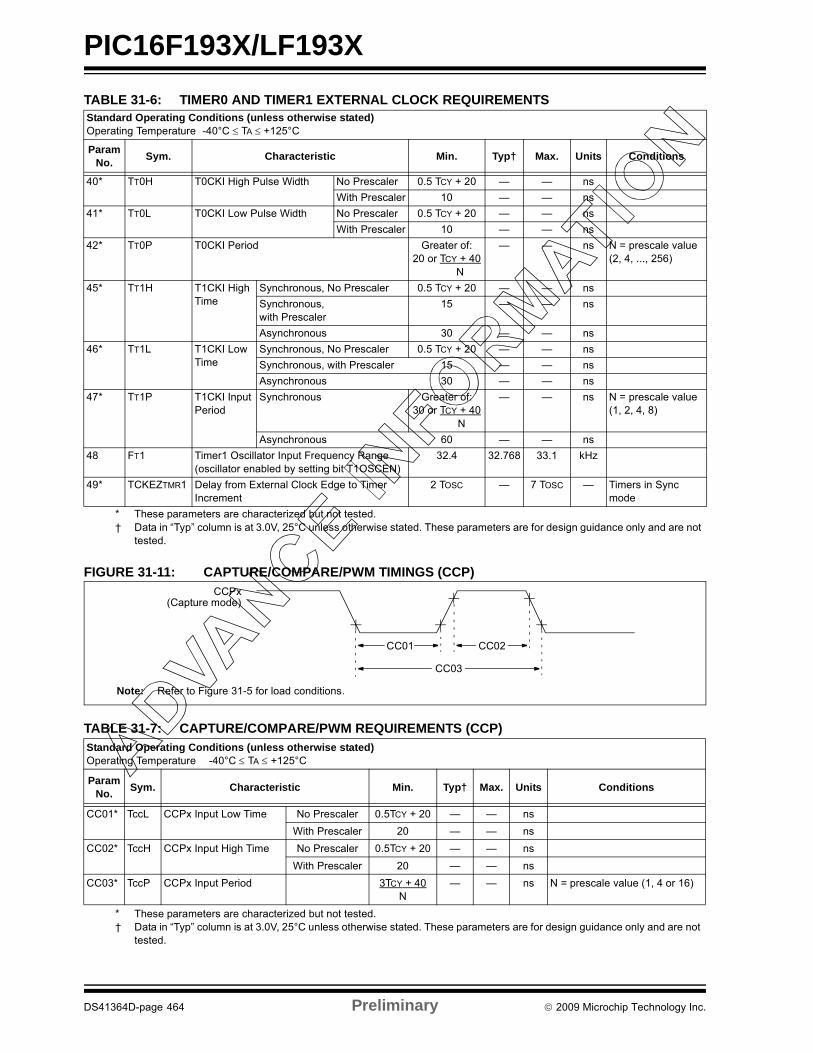
PIC16F193X/LF193X
TABLE 31-6: TIMER0 AND TIMER1 EXTERNAL CLOCK REQUIREMENTS
FIGURE 31-11: CAPTURE/COMPARE/PWM TIMINGS (CCP)
TABLE 31-7: CAPTURE/COMPARE/PWM REQUIREMENTS (CCP)
Standard Operating Conditions (unless otherwise stated)Operating Temperature -40°C TA +125°C
Param No.
Sym. Characteristic Min. Typ† Max. Units Conditions
40* TT0H T0CKI High Pulse Width No Prescaler 0.5 TCY + 20 — — ns
With Prescaler 10 — — ns
41* TT0L T0CKI Low Pulse Width No Prescaler 0.5 TCY + 20 — — ns
With Prescaler 10 — — ns
42* TT0P T0CKI Period Greater of:20 or TCY + 40
N
— — ns N = prescale value (2, 4, ..., 256)
45* TT1H T1CKI High Time
Synchronous, No Prescaler 0.5 TCY + 20 — — ns
Synchronous, with Prescaler
15 — — ns
Asynchronous 30 — — ns
46* TT1L T1CKI Low Time
Synchronous, No Prescaler 0.5 TCY + 20 — — ns
Synchronous, with Prescaler 15 — — ns
Asynchronous 30 — — ns
47* TT1P T1CKI Input Period
Synchronous Greater of:30 or TCY + 40
N
— — ns N = prescale value (1, 2, 4, 8)
Asynchronous 60 — — ns
48 FT1 Timer1 Oscillator Input Frequency Range (oscillator enabled by setting bit T1OSCEN)
32.4 32.768 33.1 kHz
49* TCKEZTMR1 Delay from External Clock Edge to Timer Increment
2 TOSC — 7 TOSC — Timers in Sync mode
* These parameters are characterized but not tested.† Data in “Typ” column is at 3.0V, 25°C unless otherwise stated. These parameters are for design guidance only and are not
tested.
Standard Operating Conditions (unless otherwise stated)Operating Temperature -40°C TA +125°C
Param No.
Sym. Characteristic Min. Typ† Max. Units Conditions
CC01* TccL CCPx Input Low Time No Prescaler 0.5TCY + 20 — — ns
With Prescaler 20 — — ns
CC02* TccH CCPx Input High Time No Prescaler 0.5TCY + 20 — — ns
With Prescaler 20 — — ns
CC03* TccP CCPx Input Period 3TCY + 40N
— — ns N = prescale value (1, 4 or 16)
* These parameters are characterized but not tested.† Data in “Typ” column is at 3.0V, 25°C unless otherwise stated. These parameters are for design guidance only and are not
tested.
Note: Refer to Figure 31-5 for load conditions.
(Capture mode)
CC01 CC02
CC03
CCPx
DS41364D-page 464 Preliminary 2009 Microchip Technology Inc.
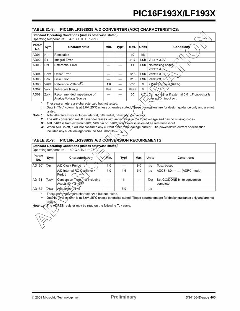
PIC16F193X/LF193X
TABLE 31-8: PIC16F/LF1938/39 A/D CONVERTER (ADC) CHARACTERISTICS:
TABLE 31-9: PIC16F/LF1938/39 A/D CONVERSION REQUIREMENTS
Standard Operating Conditions (unless otherwise stated)Operating temperature -40°C TA +125°C
Param No.
Sym. Characteristic Min. Typ† Max. Units Conditions
AD01 NR Resolution — — 10 bit
AD02 EIL Integral Error — — ±1.7 LSb VREF = 3.0V
AD03 EDL Differential Error — — ±1 LSb No missing codesVREF = 3.0V
AD04 EOFF Offset Error — — ±2.5 LSb VREF = 3.0V
AD05 EGN Gain Error — — ±2.0 LSb VREF = 3.0V
AD06 VREF Reference Voltage(3) 1.8 — VDD V = (VREF+ minus VREF-)
AD07 VAIN Full-Scale Range VSS — VREF V
AD08 ZAIN Recommended Impedance of Analog Voltage Source
— — 50 k Can go higher if external 0.01F capacitor is present on input pin.
* These parameters are characterized but not tested.† Data in “Typ” column is at 3.0V, 25°C unless otherwise stated. These parameters are for design guidance only and are not
tested.Note 1: Total Absolute Error includes integral, differential, offset and gain errors.
2: The A/D conversion result never decreases with an increase in the input voltage and has no missing codes.3: ADC VREF is from external VREF, VDD pin or FVREF, whichever is selected as reference input.4: When ADC is off, it will not consume any current other than leakage current. The power-down current specification
includes any such leakage from the ADC module.
Standard Operating Conditions (unless otherwise stated)Operating temperature -40°C TA +125°C
ParamNo.
Sym. Characteristic Min. Typ† Max. Units Conditions
AD130* TAD A/D Clock Period 1.0 — 9.0 s TOSC-based
A/D Internal RC Oscillator Period
1.0 1.6 6.0 s ADCS<1:0> = 11 (ADRC mode)
AD131 TCNV Conversion Time (not including Acquisition Time)(1)
— 11 — TAD Set GO/DONE bit to conversioncomplete
AD132* TACQ Acquisition Time — 5.0 — s
* These parameters are characterized but not tested.† Data in “Typ” column is at 3.0V, 25°C unless otherwise stated. These parameters are for design guidance only and are not
tested.Note 1: The ADRES register may be read on the following TCY cycle.
2009 Microchip Technology Inc. Preliminary DS41364D-page 465
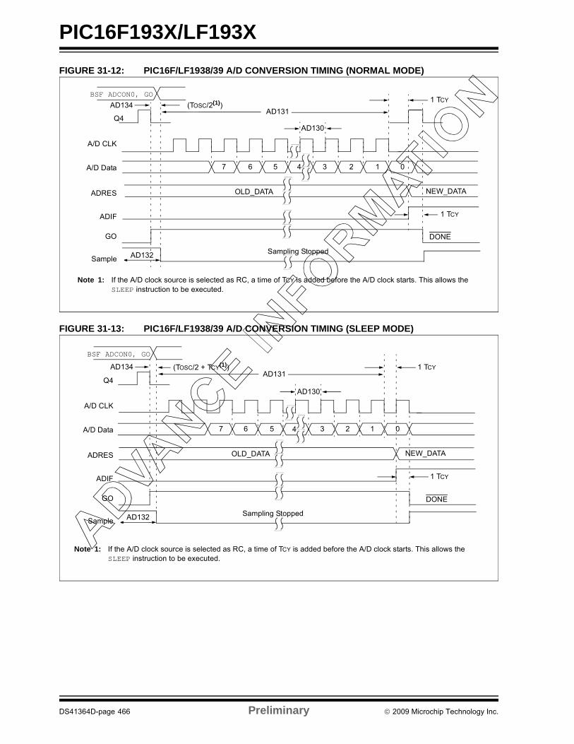
PIC16F193X/LF193X
FIGURE 31-12: PIC16F/LF1938/39 A/D CONVERSION TIMING (NORMAL MODE)
FIGURE 31-13: PIC16F/LF1938/39 A/D CONVERSION TIMING (SLEEP MODE)
AD131
AD130
BSF ADCON0, GO
Q4
A/D CLK
A/D Data
ADRES
ADIF
GO
Sample
OLD_DATA
Sampling Stopped
DONE
NEW_DATA
7 6 5 3 2 1 0
Note 1: If the A/D clock source is selected as RC, a time of TCY is added before the A/D clock starts. This allows the SLEEP instruction to be executed.
1 TCY
4
AD134 (TOSC/2(1))
1 TCY
AD132
AD132
AD131
AD130
BSF ADCON0, GO
Q4
A/D CLK
A/D Data
ADRES
ADIF
GO
Sample
OLD_DATA
Sampling Stopped
DONE
NEW_DATA
7 5 3 2 1 0
Note 1: If the A/D clock source is selected as RC, a time of TCY is added before the A/D clock starts. This allows the SLEEP instruction to be executed.
AD134
46
1 TCY(TOSC/2 + TCY(1))
1 TCY
DS41364D-page 466 Preliminary 2009 Microchip Technology Inc.

PIC16F193X/LF193X
TABLE 31-10: COMPARATOR SPECIFICATIONS
TABLE 31-11: DIGITAL-TO-ANALOG CONVERTER (DAC) SPECIFICATIONS
FIGURE 31-14: USART SYNCHRONOUS TRANSMISSION (MASTER/SLAVE) TIMING
Operating Conditions: 1.8V < VDD < 5.5V, -40°C < TA < +125°C (unless otherwise stated).
ParamNo.
Sym. Characteristics Min. Typ. Max. Units Comments
CM01 VIOFF Input Offset Voltage — ±7.5 ±60 mV
CM02 VICM Input Common Mode Voltage 0 — VDD V
CM03 CMRR Common Mode Rejection Ratio — 50 — dB
CM04 TRESP Response Time — 150 400 ns Note 1
CM05 TMC2OV Comparator Mode Change to Output Valid*
— — 10 s
CM06 CHYSTER Comparator Hysteresis — 65 — mV
* These parameters are characterized but not tested.
Note 1: Response time measured with one comparator input at VDD/2, while the other input transitions from VSS to VDD.
Operating Conditions: 1.8V < VDD < 5.5V, -40°C < TA < +125°C (unless otherwise stated).
ParamNo.
Sym. Characteristics Min. Typ. Max. Units Comments
DAC01* CLSB Step Size(2) — VDD/32 — V
DAC02* CACC Absolute Accuracy — — 1/2 LSb
DAC03* CR Unit Resistor Value (R) — TBD —
DAC04* CST Settling Time(1) — — 10 s
* These parameters are characterized but not tested.Legend: TBD = To Be Determined
Note 1: Settling time measured while DACR<4:0> transitions from ‘0000’ to ‘1111’.
Note: Refer to Figure 31-5 for load conditions.
US121 US121
US120 US122
CK
DT
2009 Microchip Technology Inc. Preliminary DS41364D-page 467
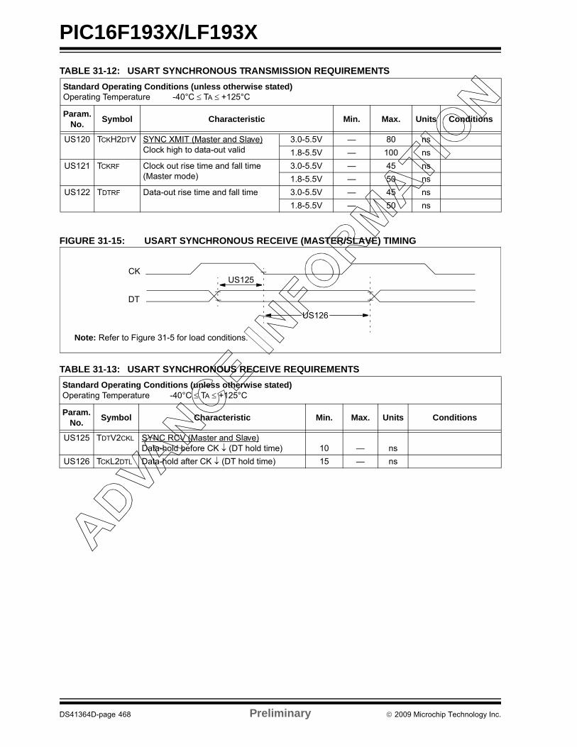
PIC16F193X/LF193X
TABLE 31-12: USART SYNCHRONOUS TRANSMISSION REQUIREMENTS
FIGURE 31-15: USART SYNCHRONOUS RECEIVE (MASTER/SLAVE) TIMING
TABLE 31-13: USART SYNCHRONOUS RECEIVE REQUIREMENTS
Standard Operating Conditions (unless otherwise stated)Operating Temperature -40°C TA +125°C
Param. No.
Symbol Characteristic Min. Max. Units Conditions
US120 TCKH2DTV SYNC XMIT (Master and Slave)Clock high to data-out valid
3.0-5.5V — 80 ns
1.8-5.5V — 100 ns
US121 TCKRF Clock out rise time and fall time (Master mode)
3.0-5.5V — 45 ns
1.8-5.5V — 50 ns
US122 TDTRF Data-out rise time and fall time 3.0-5.5V — 45 ns
1.8-5.5V — 50 ns
Standard Operating Conditions (unless otherwise stated)Operating Temperature -40°C TA +125°C
Param. No.
Symbol Characteristic Min. Max. Units Conditions
US125 TDTV2CKL SYNC RCV (Master and Slave)Data-hold before CK (DT hold time) 10 — ns
US126 TCKL2DTL Data-hold after CK (DT hold time) 15 — ns
Note: Refer to Figure 31-5 for load conditions.
US125
US126
CK
DT
DS41364D-page 468 Preliminary 2009 Microchip Technology Inc.
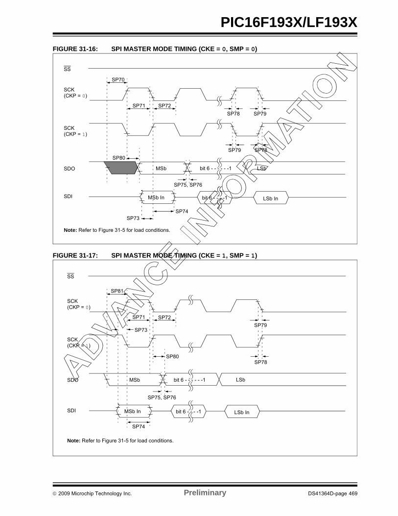
PIC16F193X/LF193X
FIGURE 31-16: SPI MASTER MODE TIMING (CKE = 0, SMP = 0)
FIGURE 31-17: SPI MASTER MODE TIMING (CKE = 1, SMP = 1)
SS
SCK(CKP = 0)
SCK(CKP = 1)
SDO
SDI
SP70
SP71 SP72
SP73SP74
SP75, SP76
SP78SP79
SP80
SP79SP78
MSb LSbbit 6 - - - - - -1
MSb In LSb Inbit 6 - - - -1
Note: Refer to Figure 31-5 for load conditions.
SS
SCK(CKP = 0)
SCK(CKP = 1)
SDO
SDI
SP81
SP71 SP72
SP74
SP75, SP76
SP78SP80
MSb
SP79SP73
MSb In
bit 6 - - - - - -1
LSb Inbit 6 - - - -1
LSb
Note: Refer to Figure 31-5 for load conditions.
2009 Microchip Technology Inc. Preliminary DS41364D-page 469

PIC16F193X/LF193X
FIGURE 31-18: SPI SLAVE MODE TIMING (CKE = 0)
FIGURE 31-19: SPI SLAVE MODE TIMING (CKE = 1)
SS
SCK(CKP = 0)
SCK(CKP = 1)
SDO
SDI
SP70
SP71 SP72
SP73
SP74
SP75, SP76 SP77
SP78SP79
SP80
SP79SP78
MSb LSbbit 6 - - - - - -1
MSb In bit 6 - - - -1 LSb In
SP83
Note: Refer to Figure 31-5 for load conditions.
SS
SCK(CKP = 0)
SCK(CKP = 1)
SDO
SDI
SP70
SP71 SP72
SP82
SP74
SP75, SP76
MSb bit 6 - - - - - -1 LSb
SP77
MSb In bit 6 - - - -1 LSb In
SP80
SP83
Note: Refer to Figure 31-5 for load conditions.
DS41364D-page 470 Preliminary 2009 Microchip Technology Inc.
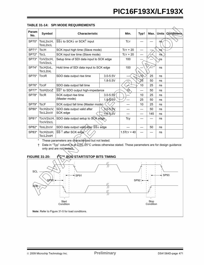
PIC16F193X/LF193X
TABLE 31-14: SPI MODE REQUIREMENTS
FIGURE 31-20: I2C™ BUS START/STOP BITS TIMING
Param No.
Symbol Characteristic Min. Typ† Max. Units Conditions
SP70* TSSL2SCH, TSSL2SCL
SS to SCK or SCK input TCY — — ns
SP71* TSCH SCK input high time (Slave mode) TCY + 20 — — ns
SP72* TSCL SCK input low time (Slave mode) TCY + 20 — — ns
SP73* TDIV2SCH, TDIV2SCL
Setup time of SDI data input to SCK edge 100 — — ns
SP74* TSCH2DIL, TSCL2DIL
Hold time of SDI data input to SCK edge 100 — — ns
SP75* TDOR SDO data output rise time 3.0-5.5V — 10 25 ns
1.8-5.5V — 25 50 ns
SP76* TDOF SDO data output fall time — 10 25 ns
SP77* TSSH2DOZ SS to SDO output high-impedance 10 — 50 ns
SP78* TSCR SCK output rise time (Master mode)
3.0-5.5V — 10 25 ns
1.8-5.5V — 25 50 ns
SP79* TSCF SCK output fall time (Master mode) — 10 25 ns
SP80* TSCH2DOV,TSCL2DOV
SDO data output valid after SCK edge
3.0-5.5V — — 50 ns
1.8-5.5V — — 145 ns
SP81* TDOV2SCH,TDOV2SCL
SDO data output setup to SCK edge Tcy — — ns
SP82* TSSL2DOV SDO data output valid after SS edge — — 50 ns
SP83* TSCH2SSH,TSCL2SSH
SS after SCK edge 1.5TCY + 40 — — ns
* These parameters are characterized but not tested.
† Data in “Typ” column is at 3.0V, 25°C unless otherwise stated. These parameters are for design guidance only and are not tested.
Note: Refer to Figure 31-5 for load conditions.
SP91
SP92
SP93SCL
SDA
StartCondition
StopCondition
SP90
2009 Microchip Technology Inc. Preliminary DS41364D-page 471

PIC16F193X/LF193X
TABLE 31-15: I2C™ BUS START/STOP BITS REQUIREMENTS
FIGURE 31-21: I2C™ BUS DATA TIMING
ParamNo.
Symbol Characteristic Min. Typ Max. Units Conditions
SP90* TSU:STA Start condition 100 kHz mode 4700 — — ns Only relevant for Repeated Start conditionSetup time 400 kHz mode 600 — —
SP91* THD:STA Start condition 100 kHz mode 4000 — — ns After this period, the first clock pulse is generatedHold time 400 kHz mode 600 — —
SP92* TSU:STO Stop condition 100 kHz mode 4700 — — ns
Setup time 400 kHz mode 600 — —
SP93 THD:STO Stop condition 100 kHz mode 4000 — — ns
Hold time 400 kHz mode 600 — —
* These parameters are characterized but not tested.
Note: Refer to Figure 31-5 for load conditions.
SP90
SP91 SP92
SP100SP101
SP103
SP106SP107
SP109SP109
SP110
SP102
SCL
SDAIn
SDAOut
DS41364D-page 472 Preliminary 2009 Microchip Technology Inc.
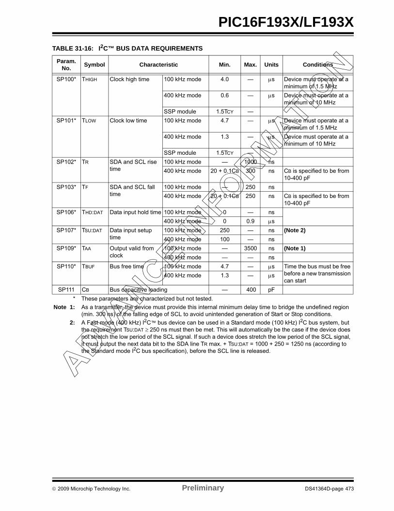
PIC16F193X/LF193X
TABLE 31-16: I2C™ BUS DATA REQUIREMENTS
Param.No.
Symbol Characteristic Min. Max. Units Conditions
SP100* THIGH Clock high time 100 kHz mode 4.0 — s Device must operate at a minimum of 1.5 MHz
400 kHz mode 0.6 — s Device must operate at a minimum of 10 MHz
SSP module 1.5TCY —
SP101* TLOW Clock low time 100 kHz mode 4.7 — s Device must operate at a minimum of 1.5 MHz
400 kHz mode 1.3 — s Device must operate at a minimum of 10 MHz
SSP module 1.5TCY —
SP102* TR SDA and SCL rise time
100 kHz mode — 1000 ns
400 kHz mode 20 + 0.1CB 300 ns CB is specified to be from 10-400 pF
SP103* TF SDA and SCL fall time
100 kHz mode — 250 ns
400 kHz mode 20 + 0.1CB 250 ns CB is specified to be from 10-400 pF
SP106* THD:DAT Data input hold time 100 kHz mode 0 — ns
400 kHz mode 0 0.9 s
SP107* TSU:DAT Data input setup time
100 kHz mode 250 — ns (Note 2)
400 kHz mode 100 — ns
SP109* TAA Output valid from clock
100 kHz mode — 3500 ns (Note 1)
400 kHz mode — — ns
SP110* TBUF Bus free time 100 kHz mode 4.7 — s Time the bus must be free before a new transmission can start
400 kHz mode 1.3 — s
SP111 CB Bus capacitive loading — 400 pF
* These parameters are characterized but not tested.
Note 1: As a transmitter, the device must provide this internal minimum delay time to bridge the undefined region (min. 300 ns) of the falling edge of SCL to avoid unintended generation of Start or Stop conditions.
2: A Fast mode (400 kHz) I2C™ bus device can be used in a Standard mode (100 kHz) I2C bus system, but the requirement TSU:DAT 250 ns must then be met. This will automatically be the case if the device does not stretch the low period of the SCL signal. If such a device does stretch the low period of the SCL signal, it must output the next data bit to the SDA line TR max. + TSU:DAT = 1000 + 250 = 1250 ns (according to the Standard mode I2C bus specification), before the SCL line is released.
2009 Microchip Technology Inc. Preliminary DS41364D-page 473
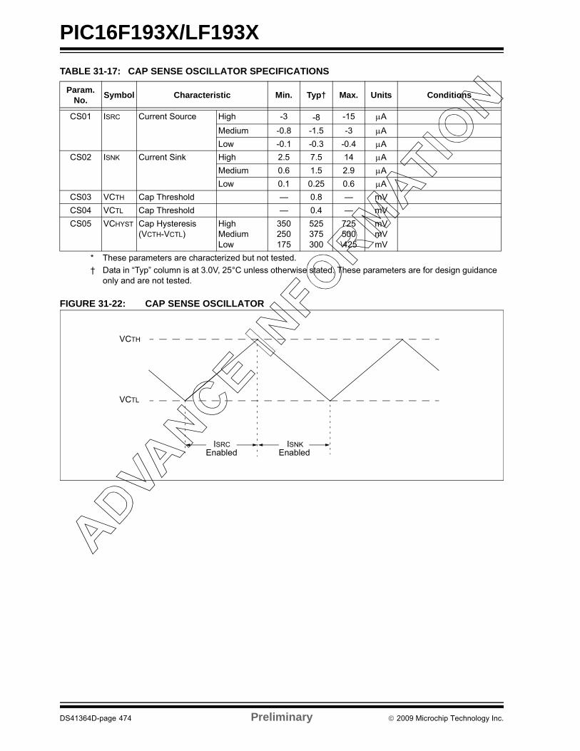
PIC16F193X/LF193X
TABLE 31-17: CAP SENSE OSCILLATOR SPECIFICATIONS
FIGURE 31-22: CAP SENSE OSCILLATOR
Param.No.
Symbol Characteristic Min. Typ† Max. Units Conditions
CS01 ISRC Current Source High -3 -8 -15 A
Medium -0.8 -1.5 -3 A
Low -0.1 -0.3 -0.4 A
CS02 ISNK Current Sink High 2.5 7.5 14 A
Medium 0.6 1.5 2.9 A
Low 0.1 0.25 0.6 A
CS03 VCTH Cap Threshold — 0.8 — mV
CS04 VCTL Cap Threshold — 0.4 — mV
CS05 VCHYST Cap Hysteresis (VCTH-VCTL)
HighMediumLow
350250175
525375300
725500\425
mVmVmV
* These parameters are characterized but not tested.
† Data in “Typ” column is at 3.0V, 25°C unless otherwise stated. These parameters are for design guidance only and are not tested.
ISRC
VCTH
VCTL
ISNKEnabledEnabled
DS41364D-page 474 Preliminary 2009 Microchip Technology Inc.
PIC16F193X/LF193X
32.0 DC AND AC CHARACTERISTICS GRAPHS AND CHARTS
Graphs and charts are not available at this time.
2009 Microchip Technology Inc. Preliminary DS41364D-page 475

PIC16F193X/LF193X
NOTES:
DS41364D-page 476 Preliminary 2009 Microchip Technology Inc.

PIC16F193X/LF193X
33.0 DEVELOPMENT SUPPORT
The PIC® microcontrollers are supported with a fullrange of hardware and software development tools:
• Integrated Development Environment
- MPLAB® IDE Software
• Assemblers/Compilers/Linkers
- MPASMTM Assembler
- MPLAB C18 and MPLAB C30 C Compilers
- MPLINKTM Object Linker/MPLIBTM Object Librarian
- MPLAB ASM30 Assembler/Linker/Library
• Simulators
- MPLAB SIM Software Simulator
• Emulators
- MPLAB ICE 2000 In-Circuit Emulator
- MPLAB REAL ICE™ In-Circuit Emulator
• In-Circuit Debugger
- MPLAB ICD 2
• Device Programmers
- PICSTART® Plus Development Programmer
- MPLAB PM3 Device Programmer
- PICkit™ 2 Development Programmer
• Low-Cost Demonstration and Development Boards and Evaluation Kits
33.1 MPLAB Integrated Development Environment Software
The MPLAB IDE software brings an ease of softwaredevelopment previously unseen in the 8/16-bit micro-controller market. The MPLAB IDE is a Windows®
operating system-based application that contains:
• A single graphical interface to all debugging tools
- Simulator
- Programmer (sold separately)
- Emulator (sold separately)
- In-Circuit Debugger (sold separately)
• A full-featured editor with color-coded context
• A multiple project manager
• Customizable data windows with direct edit of contents
• High-level source code debugging
• Visual device initializer for easy register initialization
• Mouse over variable inspection
• Drag and drop variables from source to watch windows
• Extensive on-line help
• Integration of select third party tools, such as HI-TECH Software C Compilers and IAR C Compilers
The MPLAB IDE allows you to:
• Edit your source files (either assembly or C)
• One touch assemble (or compile) and download to PIC MCU emulator and simulator tools (automatically updates all project information)
• Debug using:
- Source files (assembly or C)
- Mixed assembly and C
- Machine code
MPLAB IDE supports multiple debugging tools in asingle development paradigm, from the cost-effectivesimulators, through low-cost in-circuit debuggers, tofull-featured emulators. This eliminates the learningcurve when upgrading to tools with increased flexibilityand power.
2009 Microchip Technology Inc. Preliminary DS41364D-page 477
PIC16F193X/LF193X
33.2 MPASM Assembler
The MPASM Assembler is a full-featured, universalmacro assembler for all PIC MCUs.
The MPASM Assembler generates relocatable objectfiles for the MPLINK Object Linker, Intel® standard HEXfiles, MAP files to detail memory usage and symbolreference, absolute LST files that contain source linesand generated machine code and COFF files fordebugging.
The MPASM Assembler features include:
• Integration into MPLAB IDE projects
• User-defined macros to streamline assembly code
• Conditional assembly for multi-purpose source files
• Directives that allow complete control over the assembly process
33.3 MPLAB C18 and MPLAB C30 C Compilers
The MPLAB C18 and MPLAB C30 Code DevelopmentSystems are complete ANSI C compilers forMicrochip’s PIC18 and PIC24 families of microcon-trollers and the dsPIC30 and dsPIC33 family of digitalsignal controllers. These compilers provide powerfulintegration capabilities, superior code optimization andease of use not found with other compilers.
For easy source level debugging, the compilers providesymbol information that is optimized to the MPLAB IDEdebugger.
33.4 MPLINK Object Linker/MPLIB Object Librarian
The MPLINK Object Linker combines relocatableobjects created by the MPASM Assembler and theMPLAB C18 C Compiler. It can link relocatable objectsfrom precompiled libraries, using directives from alinker script.
The MPLIB Object Librarian manages the creation andmodification of library files of precompiled code. Whena routine from a library is called from a source file, onlythe modules that contain that routine will be linked inwith the application. This allows large libraries to beused efficiently in many different applications.
The object linker/library features include:
• Efficient linking of single libraries instead of many smaller files
• Enhanced code maintainability by grouping related modules together
• Flexible creation of libraries with easy module listing, replacement, deletion and extraction
33.5 MPLAB ASM30 Assembler, Linker and Librarian
MPLAB ASM30 Assembler produces relocatablemachine code from symbolic assembly language fordsPIC30F devices. MPLAB C30 C Compiler uses theassembler to produce its object file. The assemblergenerates relocatable object files that can then bearchived or linked with other relocatable object files andarchives to create an executable file. Notable featuresof the assembler include:
• Support for the entire dsPIC30F instruction set
• Support for fixed-point and floating-point data
• Command line interface
• Rich directive set
• Flexible macro language
• MPLAB IDE compatibility
33.6 MPLAB SIM Software Simulator
The MPLAB SIM Software Simulator allows codedevelopment in a PC-hosted environment by simulat-ing the PIC MCUs and dsPIC® DSCs on an instructionlevel. On any given instruction, the data areas can beexamined or modified and stimuli can be applied froma comprehensive stimulus controller. Registers can belogged to files for further run-time analysis. The tracebuffer and logic analyzer display extend the power ofthe simulator to record and track program execution,actions on I/O, most peripherals and internal registers.
The MPLAB SIM Software Simulator fully supportssymbolic debugging using the MPLAB C18 andMPLAB C30 C Compilers, and the MPASM andMPLAB ASM30 Assemblers. The software simulatoroffers the flexibility to develop and debug code outsideof the hardware laboratory environment, making it anexcellent, economical software development tool.
DS41364D-page 478 Preliminary 2009 Microchip Technology Inc.
PIC16F193X/LF193X
33.7 MPLAB ICE 2000 High-Performance In-Circuit Emulator
The MPLAB ICE 2000 In-Circuit Emulator is intendedto provide the product development engineer with acomplete microcontroller design tool set for PICmicrocontrollers. Software control of the MPLAB ICE2000 In-Circuit Emulator is advanced by the MPLABIntegrated Development Environment, which allowsediting, building, downloading and source debuggingfrom a single environment.
The MPLAB ICE 2000 is a full-featured emulatorsystem with enhanced trace, trigger and data monitor-ing features. Interchangeable processor modules allowthe system to be easily reconfigured for emulation ofdifferent processors. The architecture of the MPLABICE 2000 In-Circuit Emulator allows expansion tosupport new PIC microcontrollers.
The MPLAB ICE 2000 In-Circuit Emulator system hasbeen designed as a real-time emulation system withadvanced features that are typically found on moreexpensive development tools. The PC platform andMicrosoft® Windows® 32-bit operating system werechosen to best make these features available in asimple, unified application.
33.8 MPLAB REAL ICE In-Circuit Emulator System
MPLAB REAL ICE In-Circuit Emulator System isMicrochip’s next generation high-speed emulator forMicrochip Flash DSC and MCU devices. It debugs andprograms PIC® Flash MCUs and dsPIC® Flash DSCswith the easy-to-use, powerful graphical user interface ofthe MPLAB Integrated Development Environment (IDE),included with each kit.
The MPLAB REAL ICE probe is connected to the designengineer’s PC using a high-speed USB 2.0 interface andis connected to the target with either a connectorcompatible with the popular MPLAB ICD 2 system(RJ11) or with the new high-speed, noise tolerant, Low-Voltage Differential Signal (LVDS) interconnection(CAT5).
MPLAB REAL ICE is field upgradeable through futurefirmware downloads in MPLAB IDE. In upcomingreleases of MPLAB IDE, new devices will be supported,and new features will be added, such as software break-points and assembly code trace. MPLAB REAL ICEoffers significant advantages over competitive emulatorsincluding low-cost, full-speed emulation, real-timevariable watches, trace analysis, complex breakpoints, aruggedized probe interface and long (up to three meters)interconnection cables.
33.9 MPLAB ICD 2 In-Circuit Debugger
Microchip’s In-Circuit Debugger, MPLAB ICD 2, is apowerful, low-cost, run-time development tool,connecting to the host PC via an RS-232 or high-speedUSB interface. This tool is based on the Flash PICMCUs and can be used to develop for these and otherPIC MCUs and dsPIC DSCs. The MPLAB ICD 2 utilizesthe in-circuit debugging capability built into the Flashdevices. This feature, along with Microchip’s In-CircuitSerial ProgrammingTM (ICSPTM) protocol, offers cost-effective, in-circuit Flash debugging from the graphicaluser interface of the MPLAB Integrated DevelopmentEnvironment. This enables a designer to develop anddebug source code by setting breakpoints, single step-ping and watching variables, and CPU status andperipheral registers. Running at full speed enablestesting hardware and applications in real time. MPLABICD 2 also serves as a development programmer forselected PIC devices.
33.10 MPLAB PM3 Device Programmer
The MPLAB PM3 Device Programmer is a universal,CE compliant device programmer with programmablevoltage verification at VDDMIN and VDDMAX formaximum reliability. It features a large LCD display(128 x 64) for menus and error messages and a modu-lar, detachable socket assembly to support variouspackage types. The ICSP™ cable assembly is includedas a standard item. In Stand-Alone mode, the MPLABPM3 Device Programmer can read, verify and programPIC devices without a PC connection. It can also setcode protection in this mode. The MPLAB PM3connects to the host PC via an RS-232 or USB cable.The MPLAB PM3 has high-speed communications andoptimized algorithms for quick programming of largememory devices and incorporates an SD/MMC card forfile storage and secure data applications.
2009 Microchip Technology Inc. Preliminary DS41364D-page 479

PIC16F193X/LF193X
33.11 PICSTART Plus Development Programmer
The PICSTART Plus Development Programmer is aneasy-to-use, low-cost, prototype programmer. Itconnects to the PC via a COM (RS-232) port. MPLABIntegrated Development Environment software makesusing the programmer simple and efficient. ThePICSTART Plus Development Programmer supportsmost PIC devices in DIP packages up to 40 pins.Larger pin count devices, such as the PIC16C92X andPIC17C76X, may be supported with an adapter socket.The PICSTART Plus Development Programmer is CEcompliant.
33.12 PICkit 2 Development Programmer
The PICkit™ 2 Development Programmer is a low-costprogrammer and selected Flash device debugger withan easy-to-use interface for programming many ofMicrochip’s baseline, mid-range and PIC18F families ofFlash memory microcontrollers. The PICkit 2 Starter Kitincludes a prototyping development board, twelvesequential lessons, software and HI-TECH’s PICC™Lite C compiler, and is designed to help get up to speedquickly using PIC® microcontrollers. The kit provideseverything needed to program, evaluate and developapplications using Microchip’s powerful, mid-rangeFlash memory family of microcontrollers.
33.13 Demonstration, Development and Evaluation Boards
A wide variety of demonstration, development andevaluation boards for various PIC MCUs and dsPICDSCs allows quick application development on fully func-tional systems. Most boards include prototyping areas foradding custom circuitry and provide application firmwareand source code for examination and modification.
The boards support a variety of features, including LEDs,temperature sensors, switches, speakers, RS-232interfaces, LCD displays, potentiometers and additionalEEPROM memory.
The demonstration and development boards can beused in teaching environments, for prototyping customcircuits and for learning about various microcontrollerapplications.
In addition to the PICDEM™ and dsPICDEM™ demon-stration/development board series of circuits, Microchiphas a line of evaluation kits and demonstration softwarefor analog filter design, KEELOQ® security ICs, CAN,IrDA®, PowerSmart battery management, SEEVAL®
evaluation system, Sigma-Delta ADC, flow ratesensing, plus many more.
Check the Microchip web page (www.microchip.com)for the complete list of demonstration, developmentand evaluation kits.
DS41364D-page 480 Preliminary 2009 Microchip Technology Inc.

PIC16F193X/LF193X
34.0 PACKAGING INFORMATION
34.1 Package Marking Information
* Standard PICmicro® device marking consists of Microchip part number, year code, week code andtraceability code. For PICmicro device marking beyond this, certain price adders apply. Please checkwith your Microchip Sales Office. For QTP devices, any special marking adders are included in QTPprice.
Legend: XX...X Customer-specific informationY Year code (last digit of calendar year)YY Year code (last 2 digits of calendar year)WW Week code (week of January 1 is week ‘01’)NNN Alphanumeric traceability code Pb-free JEDEC designator for Matte Tin (Sn)* This package is Pb-free. The Pb-free JEDEC designator ( )
can be found on the outer packaging for this package.
Note: In the event the full Microchip part number cannot be marked on one line, it willbe carried over to the next line, thus limiting the number of availablecharacters for customer-specific information.
3e
3e
3e
28-Lead SPDIP
XXXXXXXXXXXXXXXXXXXXXXXXXXXXXXXXXX
YYWWNNN
Example
PIC16F1936
0810017-I/SP
3e
40-Lead PDIP
XXXXXXXXXXXXXXXXXXXXXXXXXXXXXXXXXXXX
XXXXXXXXXXXXXXXXXXYYWWNNN
Example
PIC16F1937
0810017-I/P
Example28-Lead QFN/UQFN
XXXXXXXXXXXXXXXXYYWWNNN
16F1936-I/ML0810017
3e
2009 Microchip Technology Inc. Preliminary DS41364D-page 481

PIC16F193X/LF193X
Package Marking Information (Continued)
3e
28-Lead SOIC
XXXXXXXXXXXXXXXXXXXXXXXXXXXXXXXXXXXXXXXXXXXXXXXXXXXXXXXXXXXX
YYWWNNN
Example
0810017
28-Lead SSOP
XXXXXXXXXXXXXXXXXXXXXXXX
YYWWNNN
Example
PIC16F1936
0810017
XXXXXXXXXX
44-Lead QFN
XXXXXXXXXXXXXXXXXXXX
YYWWNNN
Example
PIC16F1937-I/ML
0810017
44-Lead TQFP
XXXXXXXXXXXXXXXXXXXXXXXXXXXXXXXXX
YYWWNNN
Example
PIC16F1937
0810017
-I/SO 3e
PIC16F1936
-I/SS 3e
-I/PT 3e
DS41364D-page 482 Preliminary 2009 Microchip Technology Inc.
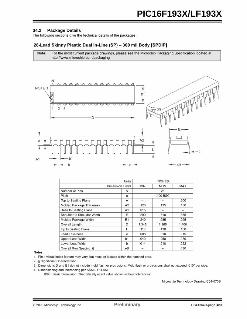
PIC16F193X/LF193X
34.2 Package DetailsThe following sections give the technical details of the packages.
��������� ������������� ��� ��������������������
!����"�� ������ �!"�����#�$�%��&"��'��� ��(�)"&�'"!&�)�����&�#�*�&����&�����&���#������� +������%����&�,����&��!&���-� ��'��!��!�����#�.��#��&�����"#��'�#�%��!����&"!��!����#�%��!����&"!��!�!������&��$���#�����/����!�#���� ��'��!��������#�&���������������.�0������
1�,2 1�!�����'��!���� ���&��������$��&� ��"��!�*��*�&�"&�&������!�
!���" 3�&���'!&��"��&����4����#�*���!(�����!��!���&��������������4�����������%���&������&�#��&��&&�255***�'��������'5���4�����
6��&! �7,8.���'��!���9�'�&! ��7 7:� ��;
7"')��%����! 7 �<��&�� � �����1�, ��&����&��������� � = = ������#�#����4���� ���4��!! �� ���� ��-� ����1�!��&����&��������� �� ���� = =��"�#��&���"�#��>�#&� . ���� �-�� �--���#�#����4����>�#&� .� ���� ��<� ����: �����9���&� � ��-�� ��-?� ����� ���&����&��������� 9 ���� ��-� ����9��#� ���4��!! � ���< ���� ����6����9��#�>�#&� )� ���� ���� ����9*��9��#�>�#&� ) ���� ���< ����: ������*����������+ �1 = = ��-�
NOTE 1
N
1 2
D
E1
eB
c
E
L
A2
eb
b1A1
A
3
������� ������� ��*��� ,������1
2009 Microchip Technology Inc. Preliminary DS41364D-page 483
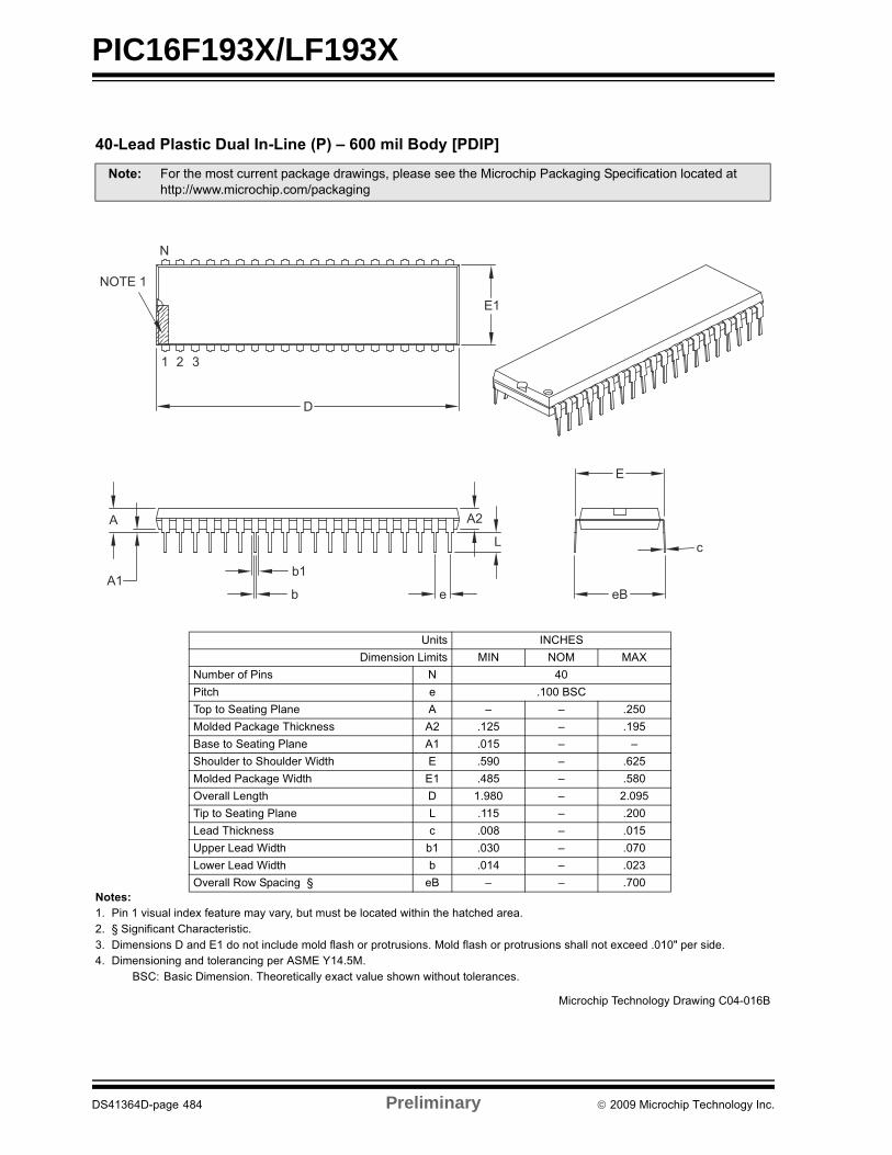
PIC16F193X/LF193X
#������������������ ��� �����$��������������
!����"�� ������ �!"�����#�$�%��&"��'��� ��(�)"&�'"!&�)�����&�#�*�&����&�����&���#������� +������%����&�,����&��!&���-� ��'��!��!�����#�.��#��&�����"#��'�#�%��!����&"!��!����#�%��!����&"!��!�!������&��$���#�����/����!�#���� ��'��!��������#�&���������������.�0������
1�,2 1�!�����'��!���� ���&��������$��&� ��"��!�*��*�&�"&�&������!�
!���" 3�&���'!&��"��&����4����#�*���!(�����!��!���&��������������4�����������%���&������&�#��&��&&�255***�'��������'5���4�����
6��&! �7,8.���'��!���9�'�&! ��7 7:� ��;
7"')��%����! 7 ����&�� � �����1�, ��&����&��������� � = = ������#�#����4���� ���4��!! �� ���� = ����1�!��&����&��������� �� ���� = =��"�#��&���"�#��>�#&� . ���� = �?����#�#����4����>�#&� .� ��<� = ��<�: �����9���&� � ���<� = ����� ���&����&��������� 9 ���� = ����9��#� ���4��!! � ���< = ����6����9��#�>�#&� )� ��-� = ����9*��9��#�>�#&� ) ���� = ���-: ������*����������+ �1 = = ����
N
NOTE 1
E1
D
1 2 3
A
A1b1
b e
c
eB
E
L
A2
������� ������� ��*��� ,�����?1
DS41364D-page 484 Preliminary 2009 Microchip Technology Inc.
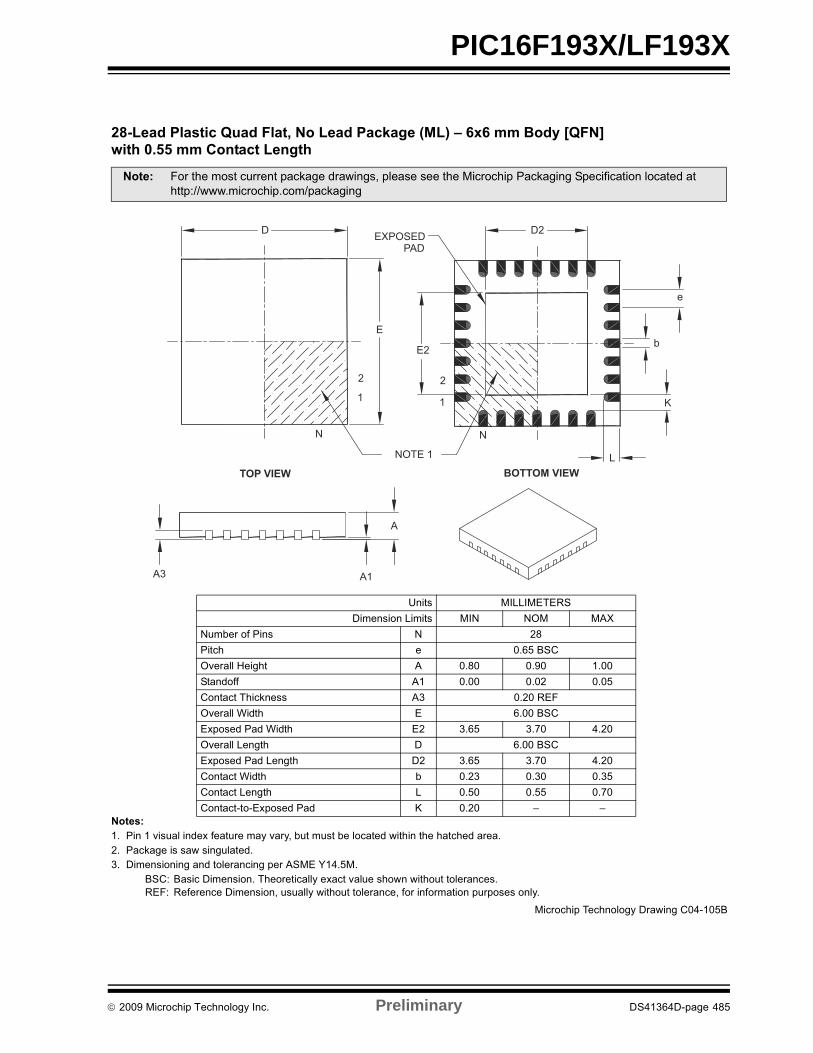
PIC16F193X/LF193X
��������������%���&���'!����������(��)���$*$�������%&! +��,�-..��/� ������ (�,
!����"�� ������ �!"�����#�$�%��&"��'��� ��(�)"&�'"!&�)�����&�#�*�&����&�����&���#������� ���4�����!�!�*�!���"��&�#�-� ��'��!��������#�&���������������.�0������
1�,2 1�!�����'��!���� ���&��������$��&� ��"��!�*��*�&�"&�&������!��.32 ��%��������'��!��(�"!"�����*�&�"&�&������(�%���%'�&����"�!�!�����
!���" 3�&���'!&��"��&����4����#�*���!(�����!��!���&��������������4�����������%���&������&�#��&��&&�255***�'��������'5���4�����
6��&! ��99��. .����'��!���9�'�&! ��7 7:� ��;
7"')��%����! 7 �<��&�� � ��?��1�,: �����8����& � ��<� ���� �����&��#%%� �� ���� ���� ����,�&��&� ���4��!! �- ������.3: �����>�#&� . ?����1�,.$�!�#���#�>�#&� .� -�?� -��� ����: �����9���&� � ?����1�,.$�!�#���#�9���&� �� -�?� -��� ����,�&��&�>�#&� ) ���- ��-� ��-�,�&��&�9���&� 9 ���� ���� ����,�&��&�&�.$�!�#���# @ ���� = =
D EXPOSED D2
e
b
K
E2
E
L
N
NOTE 1
1
22
1
N
A
A1A3
TOP VIEW BOTTOM VIEW
PAD
������� ������� ��*��� ,������1
2009 Microchip Technology Inc. Preliminary DS41364D-page 485
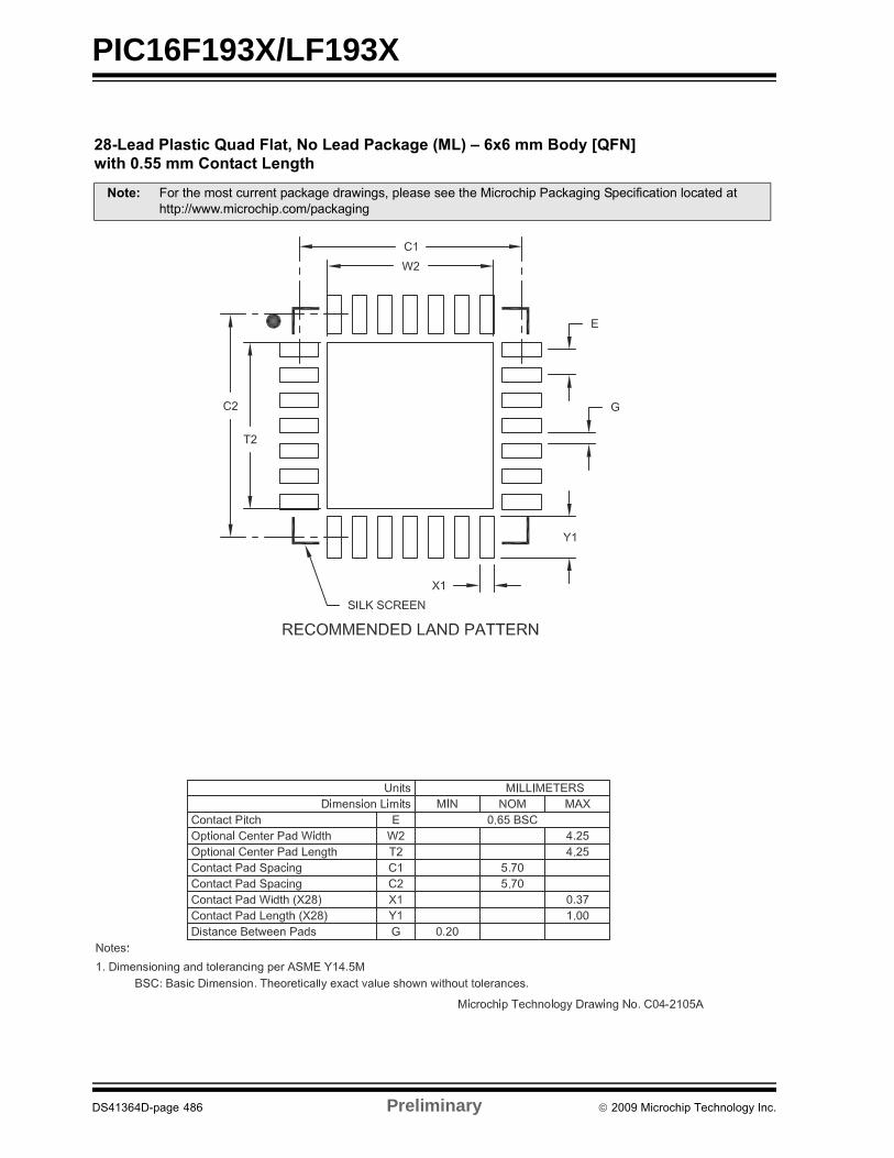
PIC16F193X/LF193X
��������������%���&���'!����������(��)���$*$�������%&! +��,�-..��/� ������ (�,
!���" 3�&���'!&��"��&����4����#�*���!(�����!��!���&��������������4�����������%���&������&�#��&��&&�255***�'��������'5���4�����
DS41364D-page 486 Preliminary 2009 Microchip Technology Inc.

PIC16F193X/LF193X
Note: For the most current package drawings, please see the Microchip Packaging Specification located at http://www.microchip.com/packaging
2009 Microchip Technology Inc. Preliminary DS41364D-page 487
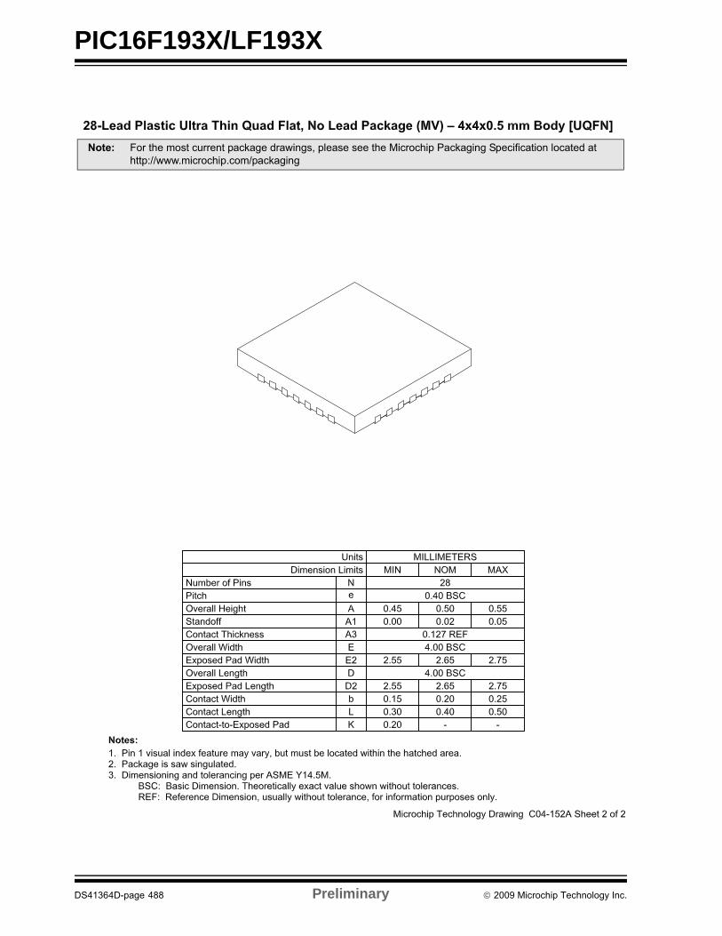
PIC16F193X/LF193X
Note: For the most current package drawings, please see the Microchip Packaging Specification located at http://www.microchip.com/packaging
DS41364D-page 488 Preliminary 2009 Microchip Technology Inc.
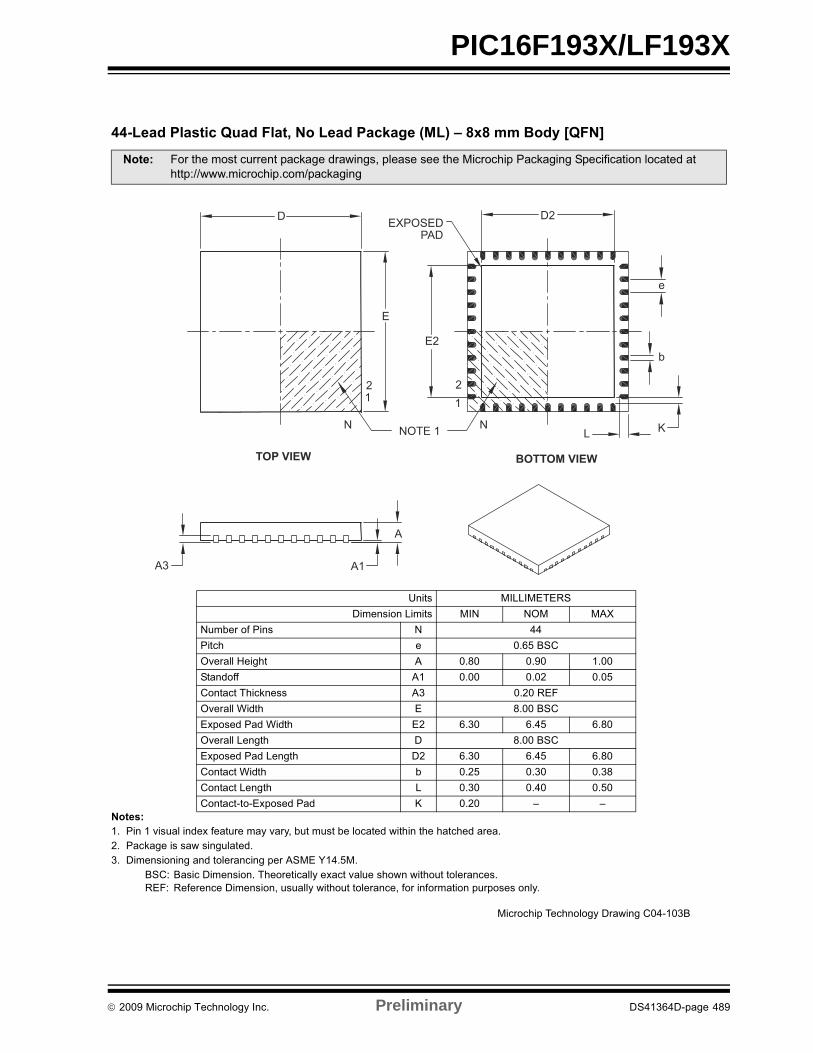
PIC16F193X/LF193X
##������������%���&���'!����������(��)����*��������%&!
!����"�� ������ �!"�����#�$�%��&"��'��� ��(�)"&�'"!&�)�����&�#�*�&����&�����&���#������� ���4�����!�!�*�!���"��&�#�-� ��'��!��������#�&���������������.�0������
1�,2 1�!�����'��!���� ���&��������$��&� ��"��!�*��*�&�"&�&������!��.32 ��%��������'��!��(�"!"�����*�&�"&�&������(�%���%'�&����"�!�!�����
!���" 3�&���'!&��"��&����4����#�*���!(�����!��!���&��������������4�����������%���&������&�#��&��&&�255***�'��������'5���4�����
6��&! ��99��. .����'��!���9�'�&! ��7 7:� ��;
7"')��%����! 7 ����&�� � ��?��1�,: �����8����& � ��<� ���� �����&��#%%� �� ���� ���� ����,�&��&� ���4��!! �- ������.3: �����>�#&� . <����1�,.$�!�#���#�>�#&� .� ?�-� ?��� ?�<�: �����9���&� � <����1�,.$�!�#���#�9���&� �� ?�-� ?��� ?�<�,�&��&�>�#&� ) ���� ��-� ��-<,�&��&�9���&� 9 ��-� ���� ����,�&��&�&�.$�!�#���# @ ���� = =
D EXPOSEDPAD
D2
e
b
KL
E2
21
NNOTE 1
21
E
N
BOTTOM VIEWTOP VIEW
A3 A1
A
������� ������� ��*��� ,�����-1
2009 Microchip Technology Inc. Preliminary DS41364D-page 489

PIC16F193X/LF193X
##������������%���&���'!����������(��)����*��������%&!
!���" 3�&���'!&��"��&����4����#�*���!(�����!��!���&��������������4�����������%���&������&�#��&��&&�255***�'��������'5���4�����
DS41364D-page 490 Preliminary 2009 Microchip Technology Inc.

PIC16F193X/LF193X
������������������0���� ��0��1���'2-.��������0�/
!����"�� ������ �!"�����#�$�%��&"��'��� ��(�)"&�'"!&�)�����&�#�*�&����&�����&���#������� +������%����&�,����&��!&���-� ��'��!��!�����#�.��#��&�����"#��'�#�%��!����&"!��!����#�%��!����&"!��!�!������&��$���#������''����!�#���� ��'��!��������#�&���������������.�0������
1�,2 1�!�����'��!���� ���&��������$��&� ��"��!�*��*�&�"&�&������!��.32 ��%��������'��!��(�"!"�����*�&�"&�&������(�%���%'�&����"�!�!�����
!���" 3�&���'!&��"��&����4����#�*���!(�����!��!���&��������������4�����������%���&������&�#��&��&&�255***�'��������'5���4�����
6��&! ��99��. .����'��!���9�'�&! ��7 7:� ��;
7"')��%����! 7 �<��&�� � �����1�,: �����8����& � = = ��?���#�#����4���� ���4��!! �� ���� = =�&��#%%��+ �� ���� = ��-�: �����>�#&� . ���-��1�,��#�#����4����>�#&� .� �����1�,: �����9���&� � ������1�,,��'%��A�&����B � ���� = ����3&�9���&� 9 ���� = ����3&���& 9� ������.33&������� � � �C = <C9��#� ���4��!! � ���< = ��--9��#�>�#&� ) ��-� = ������#���%&������� � � �C = ��C��#���%&�������1&&' � �C = ��C
c
hh
LL1
A2
A1
A
NOTE 1
1 2 3
be
EE1
D
φ
β
α
N
������� ������� ��*��� ,������1
2009 Microchip Technology Inc. Preliminary DS41364D-page 491
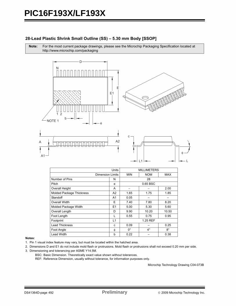
PIC16F193X/LF193X
��������������,3� �����0���� ����.-���������0�
!����"�� ������ �!"�����#�$�%��&"��'��� ��(�)"&�'"!&�)�����&�#�*�&����&�����&���#������� ��'��!��!�����#�.��#��&�����"#��'�#�%��!����&"!��!����#�%��!����&"!��!�!������&��$���#������''����!�#��-� ��'��!��������#�&���������������.�0������
1�,2 1�!�����'��!���� ���&��������$��&� ��"��!�*��*�&�"&�&������!��.32 ��%��������'��!��(�"!"�����*�&�"&�&������(�%���%'�&����"�!�!�����
!���" 3�&���'!&��"��&����4����#�*���!(�����!��!���&��������������4�����������%���&������&�#��&��&&�255***�'��������'5���4�����
6��&! ��99��. .����'��!���9�'�&! ��7 7:� ��;
7"')��%����! 7 �<��&�� � ��?��1�,: �����8����& � = = ������#�#����4���� ���4��!! �� ��?� ���� ��<��&��#%%� �� ���� = =: �����>�#&� . ���� ��<� <�����#�#����4����>�#&� .� ���� ��-� ��?�: �����9���&� � ���� ����� �����3&�9���&� 9 ���� ���� ����3&���& 9� ������.39��#� ���4��!! � ���� = ����3&������ � �C �C <C9��#�>�#&� ) ���� = ��-<
LL1
cA2
A1
A
EE1
D
N
1 2
NOTE 1b
e
φ
������� ������� ��*��� ,�����-1
DS41364D-page 492 Preliminary 2009 Microchip Technology Inc.
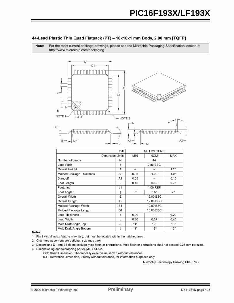
PIC16F193X/LF193X
##������������4,� %���&���5�����4��6�*6�*6������'�-�����4%&�
!����"�� ������ �!"�����#�$�%��&"��'��� ��(�)"&�'"!&�)�����&�#�*�&����&�����&���#������� ,��'%�!��&����!�����&����D�!�E��'��� ���-� ��'��!��!������#�.��#��&�����"#��'�#�%��!����&"!��!����#�%��!����&"!��!�!������&��$���#������''����!�#���� ��'��!��������#�&���������������.�0������
1�,2 1�!�����'��!���� ���&��������$��&� ��"��!�*��*�&�"&�&������!��.32 ��%��������'��!��(�"!"�����*�&�"&�&������(�%���%'�&����"�!�!�����
!���" 3�&���'!&��"��&����4����#�*���!(�����!��!���&��������������4�����������%���&������&�#��&��&&�255***�'��������'5���4�����
6��&! ��99��. .����'��!���9�'�&! ��7 7:� ��;
7"')��%�9��#! 7 ��9��#���&�� � ��<��1�,: �����8����& � = = ������#�#����4���� ���4��!! �� ���� ���� �����&��#%%�� �� ���� = ����3&�9���&� 9 ���� ��?� ����3&���& 9� ������.33&������ � �C -��C �C: �����>�#&� . ������1�,: �����9���&� � ������1�,��#�#����4����>�#&� .� ������1�,��#�#����4����9���&� �� ������1�,9��#� ���4��!! � ���� = ����9��#�>�#&� ) ��-� ��-� ������#���%&������� � � ��C ��C �-C��#���%&�������1&&' � ��C ��C �-C
A
E
E1
DD1
e
b
NOTE 1NOTE 2
N
1 2 3
c
A1L
A2L1
α
φ
β
������� ������� ��*��� ,�����?1
2009 Microchip Technology Inc. Preliminary DS41364D-page 493
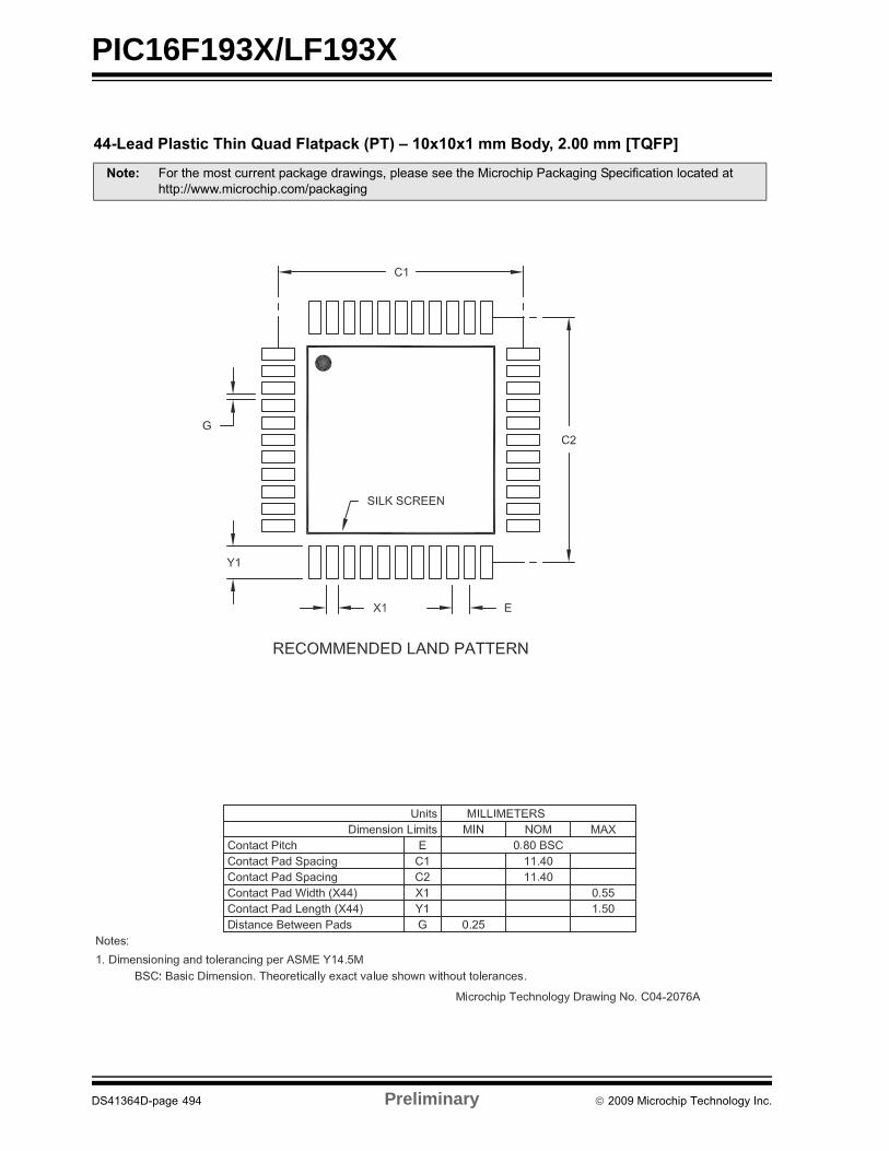
PIC16F193X/LF193X
##������������4,� %���&���5�����4��6�*6�*6������'�-�����4%&�
!���" 3�&���'!&��"��&����4����#�*���!(�����!��!���&��������������4�����������%���&������&�#��&��&&�255***�'��������'5���4�����
DS41364D-page 494 Preliminary 2009 Microchip Technology Inc.

PIC16F193X/LF193X
APPENDIX A: DATA SHEET REVISION HISTORY
Revision A
Original release (12/2008)
Revision B (04/2009)
Revised data sheet title; Revised Features section.
Revision C (12/2009)
Added PIC16L/LF1933/34. General updates.
APPENDIX B: MIGRATING FROM OTHER PIC® DEVICES
This discusses some of the issues in migrating fromother PIC® devices to the PIC16F193X/LF193X familyof devices.
B.1 PIC16F917 to PIC16F193X/LF193X
TABLE B-1: FEATURE COMPARISON
Feature PIC16F917 PIC16F1937
Max. Operating Speed 20 MHz 32 MHz
Max. Program Memory (Words)
8K 8K
Max. SRAM (Bytes) 368 512
A/D Resolution 10-bit 10-bit
Timers (8/16-bit) 2/1 4/1
Oscillator Modes 4 8
Brown-out Reset Y Y
Internal Pull-ups RB<7:0> RB<7:0>
Interrupt-on-change RB<7:4> RB<7:0>
Comparator 2 2
AUSART/EUSART 1/0 0/1
Extended WDT Y Y
Software Control Option of WDT/BOR
N Y
INTOSC Frequencies 30 kHz - 8 MHz
500 kHz - 32 MHz
Clock Switching Y Y
Capacitive Sensing N Y
CCP/ECCP 2/0 2/3
Enhanced PIC16 CPU N Y
MSSP/SSP 0/1 1/0
LCD Y Y
2009 Microchip Technology Inc. Preliminary DS41364D-page 495
PIC16F193X/LF193X
NOTES:
DS41364D-page 496 Preliminary 2009 Microchip Technology Inc.
PIC16F193X/LF193X
INDEX
AA/D
Specifications............................................ 399, 431, 463Absolute Maximum Ratings (PIC16F/LF1933) ................. 377Absolute Maximum Ratings (PIC16F/LF1934/36/37) ....... 409Absolute Maximum Ratings (PIC16F/LF1938/39) ............ 441AC Characteristics
Industrial and Extended .................................... 424, 456Industrial and Extended (PIC16F/LF1933) ............... 392Load Conditions ........................................ 391, 423, 455
ACKSTAT ......................................................................... 270ACKSTAT Status Flag ...................................................... 270ADC .................................................................................. 153
Acquisition Requirements ......................................... 163Associated registers.................................................. 165Block Diagram........................................................... 153Calculating Acquisition Time..................................... 163Channel Selection..................................................... 154Configuration............................................................. 154Configuring Interrupt ................................................. 158Conversion Clock...................................................... 154Conversion Procedure .............................................. 158Internal Sampling Switch (RSS) Impedance.............. 163Interrupts................................................................... 156Operation .................................................................. 157Operation During Sleep ............................................ 157Port Configuration ..................................................... 154Reference Voltage (VREF)......................................... 154Source Impedance.................................................... 163Special Event Trigger................................................ 157Starting an A/D Conversion ...................................... 156
ADCON0 Register....................................................... 40, 159ADCON1 Register....................................................... 40, 160ADDFSR ........................................................................... 367ADDWFC .......................................................................... 367ADRESH Register............................................................... 40ADRESH Register (ADFM = 0) ......................................... 161ADRESH Register (ADFM = 1) ......................................... 162ADRESL Register (ADFM = 0).......................................... 161ADRESL Register (ADFM = 1).......................................... 162Alternate Pin Function....................................................... 127Analog-to-Digital Converter. See ADCANSELA Register ............................................................. 131ANSELB Register ............................................................. 135ANSELD Register ............................................................. 142ANSELE Register ............................................................. 145APFCON Register............................................................. 128Assembler
MPASM Assembler................................................... 476
BBAUDCON Register.......................................................... 298BF ............................................................................. 270, 272BF Status Flag .......................................................... 270, 272Block Diagram
Capacitive Sensing ........................................... 315, 316Block Diagrams
(CCP) Capture Mode Operation ............................... 208ADC .......................................................................... 153ADC Transfer Function ............................................. 164Analog Input Model ........................................... 164, 177CCP PWM................................................................. 212Clock Source............................................................... 67
Comparator............................................................... 174Compare................................................................... 210Crystal Operation.................................................. 69, 70Digital-to-Analog Converter (DAC) ........................... 168EUSART Receive ..................................................... 288EUSART Transmit .................................................... 287External RC Mode ...................................................... 70Fail-Safe Clock Monitor (FSCM)................................. 78Generic I/O Port........................................................ 127Interrupt Logic............................................................. 91LCD Bias Voltage Generation .................................. 333LCD Clock Generation.............................................. 332On-Chip Reset Circuit................................................. 83Peripheral Interrupt Logic ........................................... 92PIC16F193X/LF193X ........................................... 14, 22PWM (Enhanced) ..................................................... 216Resonator Operation .................................................. 69Timer0 ...................................................................... 187Timer1 ...................................................................... 191Timer1 Gate.............................................. 196, 197, 198Timer2/4/6 ................................................................ 203Voltage Reference.................................................... 151Voltage Reference Output Buffer Example .............. 168
BORCON Register.............................................................. 85BRA .................................................................................. 368Break Character (12-bit) Transmit and Receive ............... 307Brown-out Reset (BOR)...................................................... 85
Specifications ........................................... 397, 429, 461Timing and Characteristics ....................... 396, 428, 460
CC Compilers
MPLAB C18.............................................................. 476MPLAB C30.............................................................. 476
CALL................................................................................. 369CALLW ............................................................................. 369Capacitive Sensing ........................................................... 315
Associated registers w/ Capacitive Sensing............. 323Specifications ........................................... 408, 440, 472
Capture Module. See Enhanced Capture/Compare/PWM(ECCP)
Capture/Compare/PWM ................................................... 207Capture/Compare/PWM (CCP)
Associated Registers w/ Capture ............................. 209Associated Registers w/ Compare ........................... 211Associated Registers w/ PWM ......................... 215, 228Capture Mode........................................................... 208CCPx Pin Configuration............................................ 208Compare Mode......................................................... 210
CCPx Pin Configuration.................................... 210Software Interrupt Mode........................... 208, 210Special Event Trigger ....................................... 210Timer1 Mode Resource ............................ 208, 210
Prescaler .................................................................. 208PWM Mode
Duty Cycle ........................................................ 213Effects of Reset ................................................ 215Example PWM Frequencies and
Resolutions, 20 MHZ................................ 214Example PWM Frequencies and
Resolutions, 32 MHZ................................ 214Example PWM Frequencies and
Resolutions, 8 MHz .................................. 214Operation in Sleep Mode.................................. 215
2009 Microchip Technology Inc. Preliminary DS41364D-page 497
PIC16F193X/LF193X
Resolution ......................................................... 214System Clock Frequency Changes................... 215
PWM Operation ........................................................ 212PWM Overview ......................................................... 212PWM Period.............................................................. 213PWM Setup............................................................... 213
CCP1CON Register ...................................................... 44, 45CCPR1H Register ......................................................... 44, 45CCPR1L Register.......................................................... 44, 45CCPTMRS0 Register ........................................................ 230CCPTMRS1 Register ........................................................ 231CCPxAS Register.............................................................. 232CCPxCON (ECCPx) Register ........................................... 229Clock Accuracy with Asynchronous Operation ................. 296Clock Sources
External Modes ........................................................... 68EC ....................................................................... 68HS....................................................................... 68LP........................................................................ 68OST..................................................................... 69RC....................................................................... 70XT ....................................................................... 68
Internal Modes ............................................................ 71HFINTOSC.......................................................... 71Internal Oscillator Clock Switch Timing............... 73LFINTOSC .......................................................... 72MFINTOSC ......................................................... 71
Clock Switching................................................................... 75CMOUT Register............................................................... 179CMxCON0 Register .......................................................... 178CMxCON1 Register .......................................................... 179Code Examples
A/D Conversion......................................................... 158Changing Between Capture Prescalers .................... 208Initializing PORTA............................................. 129, 140Initializing PORTB..................................................... 133Initializing PORTC............................................. 137, 140Initializing PORTD..................................................... 140Initializing PORTE..................................................... 144Write Verify ............................................................... 123Writing to Flash Program Memory ............................ 121
ComparatorAssociated Registers ................................................ 180Operation .................................................................. 173
Comparator Module .......................................................... 173Cx Output State Versus Input Conditions ................. 175
Comparator Specifications ................................ 401, 433, 465Comparators
C2OUT as T1 Gate ................................................... 193Compare Module. See Enhanced Capture/Compare/
PWM (ECCP)CONFIG1 Register.............................................................. 62CONFIG2 Register.............................................................. 64Core Registers .................................................................... 39CPSCON0 Register .......................................................... 321CPSCON1 Register .......................................................... 322Customer Change Notification Service ............................. 503Customer Notification Service........................................... 503Customer Support ............................................................. 503
DDACCON0 (Digital-to-Analog Converter Control 0)
Register..................................................................... 170DACCON1 (Digital-to-Analog Converter Control 1)
Register..................................................................... 170Data EEPROM Memory .................................................... 113
Associated Registers ................................................ 126Code Protection........................................................ 114Reading .................................................................... 114Writing ...................................................................... 114
Data Memory ................................................................ 26, 29DC and AC Characteristics............................................... 473DC Characteristics
Extended and Industrial (PIC16F/LF1933) ............... 387Extended and Industrial (PIC16F/LF1934/36/37) ..... 419Extended and Industrial (PIC16F/LF1938/39) .......... 451Industrial and Extended (PIC16F/LF1933) ............... 380Industrial and Extended (PIC16F/LF1934/36/37) ..... 412Industrial and Extended (PIC16F/LF1938/39) .......... 444
Development Support ....................................................... 475Device Configuration .......................................................... 61
Code Protection.......................................................... 65Configuration Word..................................................... 61User ID ................................................................. 65, 66
Device Overview......................................................... 13, 109Digital-to-Analog Converter (DAC) ................................... 167
Associated Registers ................................................ 171Effects of a Reset ..................................................... 168Specifications ........................................... 401, 433, 465
EECCP/CCP. See Enhanced Capture/Compare/PWMEEADR Registers ............................................................. 113EEADRH Registers........................................................... 113EEADRL Register ............................................................. 124EEADRL Registers ........................................................... 113EECON1 Register..................................................... 113, 125EECON2 Register..................................................... 113, 126EEDATH Register............................................................. 124EEDATL Register ............................................................. 124EEPROM Data Memory
Avoiding Spurious Write ........................................... 114Write Verify ............................................................... 123
Effects of ResetPWM mode............................................................... 215
Electrical Specifications (PIC16F/LF1933) ....................... 377Electrical Specifications (PIC16F/LF1934/36/37) ............. 409Electrical Specifications (PIC16F/LF1938/39) .................. 441Enhanced Capture/Compare/PWM (ECCP)..................... 207
Enhanced PWM Mode.............................................. 216Auto-Restart ..................................................... 224Auto-shutdown.................................................. 223Direction Change in Full-Bridge Output Mode.. 222Full-Bridge Application...................................... 220Full-Bridge Mode .............................................. 220Half-Bridge Application ..................................... 219Half-Bridge Application Examples .................... 225Half-Bridge Mode.............................................. 219Output Relationships (Active-High and
Active-Low)............................................... 217Output Relationships Diagram.......................... 218Programmable Dead Band Delay..................... 225Shoot-through Current...................................... 225Start-up Considerations.................................... 227
Specifications ........................................... 398, 430, 462Enhanced Mid-range CPU.................................................. 21Enhanced Universal Synchronous Asynchronous
Receiver Transmitter (EUSART) .............................. 287Errata .................................................................................. 11EUSART ........................................................................... 287
Associated RegistersBaud Rate Generator ....................................... 300
DS41364D-page 498 Preliminary 2009 Microchip Technology Inc.
PIC16F193X/LF193X
Asynchronous Mode ................................................. 28912-bit Break Transmit and Receive .................. 307Associated Registers
Receive..................................................... 295Transmit.................................................... 291
Auto-Wake-up on Break ................................... 305Baud Rate Generator (BRG) ............................ 299Clock Accuracy ................................................. 296Receiver............................................................ 292Setting up 9-bit Mode with Address Detect....... 294Transmitter........................................................ 289
Baud Rate Generator (BRG)Auto Baud Rate Detect ..................................... 304Baud Rate Error, Calculating ............................ 299Baud Rates, Asynchronous Modes .................. 301Formulas ........................................................... 300High Baud Rate Select (BRGH Bit) .................. 299
Synchronous Master Mode ............................... 308, 312Associated Registers
Receive..................................................... 311Transmit.................................................... 309
Reception.......................................................... 310Transmission .................................................... 308
Synchronous Slave ModeAssociated Registers
Receive..................................................... 313Transmit.................................................... 312
Reception.......................................................... 313Transmission .................................................... 312
Extended Instruction SetADDFSR ................................................................... 367
FFail-Safe Clock Monitor....................................................... 78
Fail-Safe Condition Clearing ....................................... 78Fail-Safe Detection ..................................................... 78Fail-Safe Operation..................................................... 78Reset or Wake-up from Sleep..................................... 78
Firmware Instructions........................................................ 363Fixed Voltage Reference (FVR)
Associated Registers ................................................ 152Flash Program Memory .................................................... 113
Erasing...................................................................... 118Modifying................................................................... 122Writing....................................................................... 118
FSR Register39, 40, 41, 42, 43, 44, 45, 46, 47, 48, 49, 51, 52FVRCON (Fixed Voltage Reference Control) Register ..... 152
II2C Mode (MSSP)
Acknowledge Sequence Timing................................ 274Bus Collision
During a Repeated Start Condition................... 278During a Stop Condition.................................... 279
Effects of a Reset...................................................... 275I2C Clock Rate w/BRG.............................................. 281Master Mode
Operation .......................................................... 266Reception.......................................................... 272Start Condition Timing .............................. 268, 269Transmission .................................................... 270
Multi-Master Communication, Bus Collision and Arbitration .................................................. 275
Multi-Master Mode .................................................... 275Read/Write Bit Information (R/W Bit) ........................ 251Slave Mode
Transmission .................................................... 256Sleep Operation........................................................ 275Stop Condition Timing .............................................. 274
INDF Register39, 40, 41, 42, 43, 44, 45, 46, 47, 48, 49, 51, 52Indirect Addressing ............................................................. 56Instruction Format............................................................. 364Instruction Set................................................................... 363
ADDLW..................................................................... 367ADDWF .................................................................... 367ADDWFC.................................................................. 367ANDLW..................................................................... 367ANDWF .................................................................... 367BRA .......................................................................... 368CALL......................................................................... 369CALLW ..................................................................... 369LSLF ......................................................................... 371LSRF ........................................................................ 371MOVF ....................................................................... 371MOVIW ..................................................................... 372MOVLB..................................................................... 372MOVWI ..................................................................... 373OPTION.................................................................... 373RESET...................................................................... 373SUBWFB .................................................................. 375TRIS ......................................................................... 376BCF .......................................................................... 368BSF........................................................................... 368BTFSC...................................................................... 368BTFSS ...................................................................... 368CALL......................................................................... 369CLRF ........................................................................ 369CLRW ....................................................................... 369CLRWDT .................................................................. 369COMF ....................................................................... 369DECF........................................................................ 369DECFSZ ................................................................... 370GOTO ....................................................................... 370INCF ......................................................................... 370INCFSZ..................................................................... 370IORLW...................................................................... 370IORWF...................................................................... 370MOVLW .................................................................... 372MOVWF.................................................................... 372NOP.......................................................................... 373RETFIE..................................................................... 374RETLW ..................................................................... 374RETURN................................................................... 374RLF........................................................................... 374RRF .......................................................................... 375SLEEP ...................................................................... 375SUBLW..................................................................... 375SUBWF..................................................................... 375SWAPF..................................................................... 376XORLW .................................................................... 376XORWF .................................................................... 376
INTCON Register................................................................ 97Internal Oscillator Block
INTOSCSpecifications ................................... 393, 425, 457
Internal Sampling Switch (RSS) Impedance ..................... 163Internet Address ............................................................... 503Interrupt-On-Change......................................................... 147
Associated Registers................................................ 149Interrupts ............................................................................ 91
ADC .......................................................................... 158
2009 Microchip Technology Inc. Preliminary DS41364D-page 499
PIC16F193X/LF193X
Associated registers w/ Interrupts ............................. 104Configuration Word w/ Clock Sources ........................ 82Configuration Word w/ LDO ...................................... 105TMR1 ........................................................................ 195
INTOSC Specifications ..................................... 393, 425, 457IOCBF Register................................................................. 148IOCBN Register ................................................................ 148IOCBP Register................................................................. 148
LLATA Register........................................................... 130, 138LATB Register................................................................... 135LATD Register................................................................... 141LATE Register................................................................... 145LCD
Associated Registers ................................................ 358Bias Voltage Generation ................................... 333, 334Clock Source Selection............................................. 332Configuring the Module............................................. 357Disabling the Module ................................................ 357Frame Frequency...................................................... 340Interrupts................................................................... 353LCDCON Register .................................................... 326LCDPS Register........................................................ 326Multiplex Types ......................................................... 340Operation During Sleep ............................................ 355Pixel Control.............................................................. 340Prescaler ................................................................... 332Segment Enables...................................................... 340Waveform Generation ............................................... 342
LCDCON Register..................................................... 326, 327LCDCST Register ............................................................. 330LCDDATAx Registers ............................................... 331, 338LCDPS Register........................................................ 326, 328
LP Bits....................................................................... 332LCDREF Register ............................................................. 329LCDRL Register ................................................................ 338LCDSEn Registers ............................................................ 331Liquid Crystal Display (LCD) Driver .................................. 325Load Conditions ................................................ 391, 423, 455LSLF.................................................................................. 371LSRF ................................................................................. 371
MMaster Synchronous Serial Port. See MSSPMCLR .................................................................................. 86
Internal ........................................................................ 86Memory Organization
Data ...................................................................... 26, 29Program ...................................................................... 23
Microchip Internet Web Site .............................................. 503Migrating from other PIC Microcontroller Devices............. 493MOVIW.............................................................................. 372MOVLB.............................................................................. 372MOVWI.............................................................................. 373MPLAB ASM30 Assembler, Linker, Librarian ................... 476MPLAB ICD 2 In-Circuit Debugger.................................... 477MPLAB ICE 2000 High-Performance Universal
In-Circuit Emulator .................................................... 477MPLAB Integrated Development Environment Software .. 475MPLAB PM3 Device Programmer..................................... 477MPLAB REAL ICE In-Circuit Emulator System................. 477MPLINK Object Linker/MPLIB Object Librarian ................ 476MSSP................................................................................ 235
SPI Mode .................................................................. 238SSPBUF Register ..................................................... 241
SSPSR Register ....................................................... 241
OOPCODE Field Descriptions............................................. 363OPTION ............................................................................ 373OPTION Register.............................................................. 189OSCCON Register.............................................................. 80Oscillator
Associated Registers .................................................. 82Oscillator Module ................................................................ 67
EC............................................................................... 67HS............................................................................... 67INTOSC ...................................................................... 67LP ............................................................................... 67RC .............................................................................. 67XT ............................................................................... 67
Oscillator Parameters ....................................... 393, 425, 457Oscillator Specifications.................................... 392, 424, 456Oscillator Start-up Timer (OST)
Specifications ........................................... 397, 429, 461Oscillator Switching
Fail-Safe Clock Monitor .............................................. 78Two-Speed Clock Start-up.......................................... 76
OSCSTAT Register ............................................................ 81OSCTUNE Register............................................................ 82
PP1A/P1B/P1C/P1D.See Enhanced Capture/Compare/
PWM (ECCP)............................................................ 216Packaging ......................................................................... 479
Marking............................................................. 479, 480PDIP Details ............................................................. 481
PCL and PCLATH............................................................... 22PCL Register39, 40, 41, 42, 43, 44, 45, 46, 47, 48, 49, 51, 52PCLATH Register39, 40, 41, 42, 43, 44, 45, 46, 47, 48, 49, 51,
52PCON Register ............................................................. 40, 89PICSTART Plus Development Programmer..................... 478PIE1 Register................................................................ 40, 98PIE2 Register................................................................ 40, 99PIE3 Register.................................................................... 100Pin Diagram
PIC16F1933/1936/1938, PICLF1933/1936/1938, 28-pin PDIP/SOIC/SSOP ..................................... 3
PIC16F1933/1936/1938, PICLF1933/1936/1938, 28-pin QFN ........................................................... 4
PICF1934/1937/1939, PICLF1934/1937/1939, 44-pin QFN ........................................................... 7
PICF1934/1937/1939, PICLF1934/1937/1939, 44-pin TQFP ......................................................... 8
PICF1934/1937/1939,PICLF1934/1937/1939, 40-pin PDIP .......................................................... 6
Pinout DescriptionsPIC16F193X/PIC16LF193X........................................ 15
PIR1 Register ............................................................. 39, 101PIR2 Register ............................................................. 39, 102PIR3 Register ................................................................... 103PORTA ............................................................................. 129
ANSELA Register ..................................................... 129Associated Registers ................................................ 132Configuration Word w/ PORTA................................. 132PORTA Register ................................................... 39, 41Specifications ........................................... 395, 427, 459
PORTA Register ............................................................... 130PORTB ............................................................................. 133
Additional Pin Functions
DS41364D-page 500 Preliminary 2009 Microchip Technology Inc.

PIC16F193X/LF193X
Weak Pull-up .................................................... 134ANSELB Register ..................................................... 133Associated Registers ................................................ 136Interrupt-on-Change.................................................. 133P1B/P1C/P1D.See Enhanced Capture/Compare/
PWM+ (ECCP+) ............................................... 133Pin Descriptions and Diagrams................................. 134PORTB Register ................................................... 39, 41
PORTB Register ............................................................... 134PORTC ............................................................................. 137
Associated Registers ................................................ 139P1A.See Enhanced Capture/Compare/PWM+
(ECCP+) ........................................................... 137Pin Descriptions and Diagrams................................. 137PORTC Register ................................................... 39, 41Specifications............................................ 395, 427, 459
PORTC Register ............................................................... 138PORTD ............................................................................. 140
Additional Pin FunctionsANSELD Register ............................................. 140
Associated Registers ................................................ 142P1B/P1C/P1D.See Enhanced Capture/Compare/
PWM+ (ECCP+) ............................................... 140Pin Descriptions and Diagrams................................. 140PORTD Register ................................................... 39, 41
PORTD Register ............................................................... 141PORTE.............................................................................. 143
ANSELE Register ..................................................... 143Associated Registers ................................................ 146Pin Descriptions and Diagrams................................. 143PORTE Register ................................................... 39, 41
PORTE Register ............................................................... 144Power-Down Mode (Sleep) ............................................... 107
Associated Registers ................................................ 108Power-on Reset .................................................................. 84Power-up Time-out Sequence ............................................ 86Power-up Timer (PWRT) .................................................... 84
Specifications............................................ 397, 429, 461PR2 Register................................................................. 39, 47Precision Internal Oscillator Parameters........... 393, 425, 457Program Memory ................................................................ 23
Map and Stack (PIC16F1933/LF1933, PIC16F1934/LF1934) ................................... 23, 29
Map and Stack (PIC16F1936/LF1936, PIC16F1937/LF1937) ................................... 24, 29
Map and Stack (PIC16F1938/LF1938, PIC16F1939/LF1939) ................................... 25, 29
Programming, Device Instructions .................................... 363PSTRxCON Register ........................................................ 234PWM (ECCP Module)
PWM Steering........................................................... 226Steering Synchronization .......................................... 227
PWM Mode. See Enhanced Capture/Compare/PWM ...... 216PWM Steering................................................................... 226PWMxCON Register ......................................................... 233
RRCREG ............................................................................. 294RCREG Register................................................................. 42RCSTA Register ......................................................... 42, 297Reader Response ............................................................. 504Read-Modify-Write Operations ......................................... 363Register
RCREG Register....................................................... 304Registers
ADCON0 (ADC Control 0) ........................................ 159
ADCON1 (ADC Control 1) ........................................ 160ADRESH (ADC Result High) with ADFM = 0) .......... 161ADRESH (ADC Result High) with ADFM = 1) .......... 162ADRESL (ADC Result Low) with ADFM = 0)............ 161ADRESL (ADC Result Low) with ADFM = 1)............ 162ANSELA (PORTA Analog Select) ............................ 131ANSELB (PORTB Analog Select) ............................ 135ANSELD (PORTD Analog Select) ............................ 142ANSELE (PORTE Analog Select) ............................ 145APFCON (Alternate Pin Function Control) ............... 128BAUDCON (Baud Rate Control)............................... 298BORCON Brown-out Reset Control) .......................... 85CCPTMRS0 (PWM Timer Selection Control 0) ........ 230CCPTMRS1 (PWM Timer Selection Control 1) ........ 231CCPxAS (CCPx Auto-Shutdown Control) ................ 232CCPxCON (ECCPx Control) .................................... 229CMOUT (Comparator Output) .................................. 179CMxCON0 (Cx Control) ............................................ 178CMxCON1 (Cx Control 1)......................................... 179Configuration Word 1.................................................. 62Configuration Word 2.................................................. 64CPSCON0 (Capacitive Sensing Control Register 0) 321CPSCON1 (Capacitive Sensing Control Register 1) 322DACCON0 ................................................................ 170DACCON1 ................................................................ 170EEADRL (EEPROM Address) .................................. 124EECON1 (EEPROM Control 1) ................................ 125EECON2 (EEPROM Control 2) ................................ 126EEDATH (EEPROM Data) ....................................... 124EEDATL (EEPROM Data) ........................................ 124FVRCON .................................................................. 152INTCON (Interrupt Control) ........................................ 97IOCBF (Interrupt-on-Change Flag)........................... 148IOCBN (Interrupt-on-Change Negative Edge).......... 148IOCBP (Interrupt-on-Change Positive Edge)............ 148LATA (Data Latch PORTA) ...................................... 130LATB (Data Latch PORTB) ...................................... 135LATC (Data Latch PORTC) ...................................... 138LATD (Data Latch PORTD) ...................................... 141LATE (Data Latch PORTE) ...................................... 145LCDCON (LCD Control) ........................................... 327LCDCST (LCD Contrast Control) ............................. 330LCDDATAx (LCD Data) .................................... 331, 338LCDPS (LCD Phase)................................................ 328LCDREF (LCD Reference Voltage Control) ............. 329LCDRL (LCD Reference Voltage Control)................ 338LCDSEn (LCD Segment Enable) ............................. 331OPTION_REG (OPTION)......................................... 189OSCCON (Oscillator Control)..................................... 80OSCSTAT (Oscillator Status) ..................................... 81OSCTUNE (Oscillator Tuning).................................... 82PCON (Power Control Register)................................. 89PCON (Power Control) ............................................... 89PIE1 (Peripheral Interrupt Enable 1) .......................... 98PIE2 (Peripheral Interrupt Enable 2) .......................... 99PIE3 (Peripheral Interrupt Enable 3) ........................ 100PIR1 (Peripheral Interrupt Register 1) ...................... 101PIR2 (Peripheral Interrupt Request 2) ...................... 102PIR3 (Peripheral Interrupt Request 3) ...................... 103PORTA ..................................................................... 130PORTB ..................................................................... 134PORTC ..................................................................... 138PORTD ..................................................................... 141PORTE ..................................................................... 144PSTRxCON (PWM Steering Control) ....................... 234
2009 Microchip Technology Inc. Preliminary DS41364D-page 501

PIC16F193X/LF193X
PWMxCON (Enhanced PWM Control) ..................... 233RCSTA (Receive Status and Control)....................... 297Special Function, Summary ........................................ 39SRCON0 (SR Latch Control 0) ................................. 183SRCON1 (SR Latch Control 1) ................................. 184SSPADD (MSSP Address and Baud Rate,
I2C Mode).......................................................... 286SSPCON1 (MSSP Control 1).................................... 283SSPCON2 (SSP Control 2)....................................... 284SSPCON3 (SSP Control 3)....................................... 285SSPMSK (SSP Mask) ............................................... 286SSPSTAT (SSP Status) ............................................ 282STATUS...................................................................... 27T1CON (Timer1 Control)........................................... 199T1GCON (Timer1 Gate Control) ............................... 200TRISA (Tri-State PORTA) ......................................... 130TRISB (Tri-State PORTB) ......................................... 135TRISC (Tri-State PORTC) ........................................ 138TRISD (Tri-State PORTD) ........................................ 141TRISE (Tri-State PORTE) ......................................... 144TXCON ..................................................................... 205TXSTA (Transmit Status and Control) ...................... 296WDTCON (Watchdog Timer Control)........................ 111WPUB (Weak Pull-up PORTB) ................................. 136
RESET .............................................................................. 373Reset................................................................................... 83Reset Instruction ................................................................. 86Resets ................................................................................. 83
Associated Registers .................................................. 90Revision History ................................................................ 493
SShoot-through Current ...................................................... 225Software Simulator (MPLAB SIM)..................................... 476SPBRG Register ........................................................... 41, 42SPBRGH ........................................................................... 299SPBRGL............................................................................ 299Special Event Trigger........................................................ 157Special Function Registers (SFRs) ..................................... 39SPI Mode (MSSP)
Associated Registers ................................................ 245SPI Clock .................................................................. 241
SR Latch ........................................................................... 181Associated registers w/ SR Latch ............................. 185
SRCON0 Register............................................................. 183SRCON1 Register............................................................. 184SSPADD Register ....................................................... 43, 286SSPBUF Register ............................................................... 43SSPCON Register............................................................... 43SSPCON1 Register........................................................... 283SSPCON2 Register........................................................... 284SSPCON3 Register........................................................... 285SSPMSK Register............................................................. 286SSPOV.............................................................................. 272SSPOV Status Flag........................................................... 272SSPSTAT Register ..................................................... 43, 282
R/W Bit ...................................................................... 251Stack ................................................................................... 54
Accessing.................................................................... 54Reset........................................................................... 56
Stack Overflow/Underflow................................................... 86STATUS Register................................................................ 27SUBWFB........................................................................... 375
TT1CON Register.......................................................... 39, 199
T1GCON Register ............................................................ 200T2CON Register ........................................................... 39, 47Thermal Considerations (PIC16F/LF1933)....................... 390Thermal Considerations (PIC16F/LF1934/36/37) ............. 422Thermal Considerations (PIC16F/LF1938/39).................. 454Timer0............................................................................... 187
Associated Registers ................................................ 189Operation .................................................................. 187Specifications ........................................... 398, 430, 462
Timer1............................................................................... 191Associated registers ................................................. 201Asynchronous Counter Mode ................................... 193
Reading and Writing ......................................... 193Clock Source Selection............................................. 192Interrupt .................................................................... 195Operation .................................................................. 192Operation During Sleep ............................................ 195Oscillator................................................................... 193Prescaler .................................................................. 193Specifications ........................................... 398, 430, 462Timer1 Gate
Selecting Source .............................................. 193TMR1H Register ....................................................... 191TMR1L Register........................................................ 191
Timer2Associated registers ................................................. 206
Timer2/4/6......................................................................... 203Associated registers ................................................. 206
TimersTimer1
T1CON ............................................................. 199T1GCON........................................................... 200
Timer2/4/6TXCON ............................................................. 205
Timing DiagramsA/D Conversion......................................... 400, 432, 464A/D Conversion (Sleep Mode) .................. 400, 432, 464Acknowledge Sequence ........................................... 274Asynchronous Reception.......................................... 294Asynchronous Transmission..................................... 290Asynchronous Transmission (Back to Back) ............ 290Auto Wake-up Bit (WUE) During Normal Operation . 306Auto Wake-up Bit (WUE) During Sleep .................... 306Automatic Baud Rate Calibration.............................. 304Baud Rate Generator with Clock Arbitration............. 267BRG Reset Due to SDA Arbitration During Start
Condition .......................................................... 277Brown-out Reset (BOR)............................ 396, 428, 460Brown-out Reset Situations ........................................ 85Bus Collision During a Repeated Start Condition
(Case 1)............................................................ 278Bus Collision During a Repeated Start Condition
(Case 2)............................................................ 278Bus Collision During a Start Condition (SCL = 0) ..... 277Bus Collision During a Stop Condition (Case 1) ....... 279Bus Collision During a Stop Condition (Case 2) ....... 279Bus Collision During Start Condition (SDA only) ...... 276Bus Collision for Transmit and Acknowledge ........... 275CLKOUT and I/O ...................................... 394, 426, 458Clock Synchronization .............................................. 264Clock Timing............................................. 392, 424, 456Comparator Output ................................................... 173Enhanced Capture/Compare/PWM (ECCP)
.......................................................... 398, 430, 462Fail-Safe Clock Monitor (FSCM)................................. 79
DS41364D-page 502 Preliminary 2009 Microchip Technology Inc.

PIC16F193X/LF193X
First Start Bit Timing ................................................. 268Full-Bridge PWM Output ........................................... 221Half-Bridge PWM Output .................................. 219, 225I2C Bus Data ............................................. 406, 438, 470I2C Bus Start/Stop Bits.............................. 405, 437, 469I2C Master Mode (7 or 10-Bit Transmission) ............ 271I2C Master Mode (7-Bit Reception)........................... 273I2C Stop Condition Receive or Transmit Mode ......... 274INT Pin Interrupt.......................................................... 95Internal Oscillator Switch Timing................................. 74LCD Interrupt Timing in Quarter-Duty Cycle Drive.... 354LCD Sleep Entry/Exit when SLPEN = 1 or CS = 00 . 356PWM Auto-shutdown ................................................ 224
Firmware Restart .............................................. 224PWM Direction Change ............................................ 222PWM Direction Change at Near 100% Duty Cycle ... 223PWM Output (Active-High)........................................ 217PWM Output (Active-Low) ........................................ 218Repeat Start Condition.............................................. 269Reset Start-up Sequence............................................ 87Reset, WDT, OST and Power-up Timer ... 395, 427, 459Send Break Character Sequence ............................. 307SPI Master Mode (CKE = 1, SMP = 1) ..... 403, 435, 467SPI Mode (Master Mode).......................................... 241SPI Slave Mode (CKE = 0) ....................... 404, 436, 468SPI Slave Mode (CKE = 1) ....................... 404, 436, 468Synchronous Reception (Master Mode, SREN) ....... 311Synchronous Transmission....................................... 309Synchronous Transmission (Through TXEN) ........... 309Timer0 and Timer1 External Clock ........... 397, 429, 461Timer1 Incrementing Edge........................................ 195Two Speed Start-up .................................................... 77Type-A in 1/2 Mux, 1/2 Bias Drive ............................ 343Type-A in 1/2 Mux, 1/3 Bias Drive ............................ 345Type-A in 1/3 Mux, 1/2 Bias Drive ............................ 347Type-A in 1/3 Mux, 1/3 Bias Drive ............................ 349Type-A in 1/4 Mux, 1/3 Bias Drive ............................ 351Type-A/Type-B in Static Drive................................... 342Type-B in 1/2 Mux, 1/2 Bias Drive ............................ 344Type-B in 1/2 Mux, 1/3 Bias Drive ............................ 346Type-B in 1/3 Mux, 1/2 Bias Drive ............................ 348Type-B in 1/3 Mux, 1/3 Bias Drive ............................ 350Type-B in 1/4 Mux, 1/3 Bias Drive ............................ 352USART Synchronous Receive (Master/Slave)
.......................................................... 402, 434, 466USART Synchronous Transmission (Master/Slave
)......................................................... 401, 433, 465Wake-up from Interrupt ............................................. 108
Timing Diagrams and SpecificationsPLL Clock.................................................. 393, 425, 457
Timing Parameter Symbology........................... 391, 423, 455Timing Requirements
I2C Bus Data ............................................. 407, 439, 471I2C Bus Start/Stop Bits ............................. 406, 438, 470SPI Mode .................................................. 405, 437, 469
TMR0 Register .................................................................... 39TMR1H Register ................................................................. 39TMR1L Register .................................................................. 39TMR2 Register .............................................................. 39, 47TRIS.................................................................................. 376TRISA Register ........................................................... 40, 130TRISB ............................................................................... 133TRISB Register ........................................................... 40, 135TRISC ............................................................................... 137TRISC Register ........................................................... 40, 138
TRISD............................................................................... 140TRISD Register........................................................... 40, 141TRISE ............................................................................... 143TRISE Register........................................................... 40, 144Two-Speed Clock Start-up Mode........................................ 76TXCON (Timer2/4/6) Register .......................................... 205TXREG ............................................................................. 289TXREG Register ................................................................. 42TXSTA Register.......................................................... 42, 296
BRGH Bit .................................................................. 299
UUSART
Synchronous Master ModeRequirements, Synchronous Receive402, 434, 466Requirements, Synchronous Transmission
................................................. 402, 434, 466Timing Diagram, Synchronous Receive
................................................. 402, 434, 466Timing Diagram, Synchronous Transmission
................................................. 401, 433, 465
VVREF. SEE ADC Reference Voltage
WWake-up on Break ............................................................ 305Wake-up Using Interrupts ................................................. 108Watchdog Timer (WDT)...................................................... 86
Modes....................................................................... 110Specifications ........................................... 397, 429, 461
WCOL....................................................... 267, 270, 272, 274WCOL Status Flag.................................... 267, 270, 272, 274WDTCON Register ........................................................... 111WPUB Register................................................................. 136Write Protection .................................................................. 65WWW Address ................................................................. 503WWW, On-Line Support ..................................................... 11
2009 Microchip Technology Inc. Preliminary DS41364D-page 503

PIC16F193X/LF193X
NOTES:
DS41364D-page 504 Preliminary 2009 Microchip Technology Inc.
PIC16F193X/LF193X
THE MICROCHIP WEB SITE
Microchip provides online support via our WWW site atwww.microchip.com. This web site is used as a meansto make files and information easily available tocustomers. Accessible by using your favorite Internetbrowser, the web site contains the followinginformation:
• Product Support – Data sheets and errata, application notes and sample programs, design resources, user’s guides and hardware support documents, latest software releases and archived software
• General Technical Support – Frequently Asked Questions (FAQ), technical support requests, online discussion groups, Microchip consultant program member listing
• Business of Microchip – Product selector and ordering guides, latest Microchip press releases, listing of seminars and events, listings of Microchip sales offices, distributors and factory representatives
CUSTOMER CHANGE NOTIFICATION SERVICE
Microchip’s customer notification service helps keepcustomers current on Microchip products. Subscriberswill receive e-mail notification whenever there arechanges, updates, revisions or errata related to aspecified product family or development tool of interest.
To register, access the Microchip web site atwww.microchip.com, click on Customer ChangeNotification and follow the registration instructions.
CUSTOMER SUPPORT
Users of Microchip products can receive assistancethrough several channels:
• Distributor or Representative
• Local Sales Office
• Field Application Engineer (FAE)
• Technical Support
• Development Systems Information Line
Customers should contact their distributor,representative or field application engineer (FAE) forsupport. Local sales offices are also available to helpcustomers. A listing of sales offices and locations isincluded in the back of this document.
Technical support is available through the web siteat: http://support.microchip.com
2009 Microchip Technology Inc. Preliminary DS41364D-page 505

PIC16F193X/LF193X
READER RESPONSE
It is our intention to provide you with the best documentation possible to ensure successful use of your Microchip prod-uct. If you wish to provide your comments on organization, clarity, subject matter, and ways in which our documentationcan better serve you, please FAX your comments to the Technical Publications Manager at (480) 792-4150.
Please list the following information, and use this outline to provide us with your comments about this document.
To: Technical Publications Manager
RE: Reader Response
Total Pages Sent ________
From: Name
Company
Address
City / State / ZIP / Country
Telephone: (_______) _________ - _________
Application (optional):
Would you like a reply? Y N
Device: Literature Number:
Questions:
FAX: (______) _________ - _________
DS41364DPIC16F193X/LF193X
1. What are the best features of this document?
2. How does this document meet your hardware and software development needs?
3. Do you find the organization of this document easy to follow? If not, why?
4. What additions to the document do you think would enhance the structure and subject?
5. What deletions from the document could be made without affecting the overall usefulness?
6. Is there any incorrect or misleading information (what and where)?
7. How would you improve this document?
DS41364D-page 506 Preliminary 2009 Microchip Technology Inc.

2009 Microchip Technology Inc. Preliminary DS41364D-page 507
PIC16F193X/LF193X
PRODUCT IDENTIFICATION SYSTEM
To order or obtain information, e.g., on pricing or delivery, refer to the factory or the listed sales office.
PART NO. X /XX XXX
PatternPackageTemperatureRange
Device
Device: PIC16F1933, PIC16LF1933, PIC16F1933T, PIC16LF1933T(1)
PIC16F1934, PIC16LF1934, PIC16F1934T, PIC16LF1934T(1)
PIC16F1936, PIC16LF1936, PIC16F1936T, PIC16LF1936T(1)
PIC16F1937, PIC16LF1937, PIC16F1937T, PIC16LF1937T(1)
PIC16F1938, PIC16LF1938, PIC16F1938T, PIC16LF1938T(1)
PIC16F1939, PIC16LF1939, PIC16F1939T, PIC16LF1939T(1)
Temperature Range:
I = -40C to +85CE = -40C to +125C
Package: ML = Micro Lead Frame (QFN)MV = Micro Lead Frame (UQFN) 4x4P = Plastic DIPPT = TQFP (Thin Quad Flatpack)SO = SOICSP = Skinny Plastic DIPSS = SSOP
Pattern: 3-Digit Pattern Code for QTP (blank otherwise)
Examples:
a) PIC16LF1937 - I/P = Industrial temp., Plastic DIP package, low-voltage VDD limits.
b) PIC16F1934 - I/PT = Industrial temp., TQFP package, standard VDD limits.
c) PIC16F1933 - E/ML = Extended temp., QFN package, standard VDD limits.
Note 1: F = Standard Voltage RangeLF = Low Voltage Range
2: T = In tape and reel for QFN, TQFP, SOIC and SSOP packages only.

DS41364D-page 508 Preliminary 2009 Microchip Technology Inc.
AMERICASCorporate Office2355 West Chandler Blvd.Chandler, AZ 85224-6199Tel: 480-792-7200 Fax: 480-792-7277Technical Support: http://support.microchip.comWeb Address: www.microchip.com
AtlantaDuluth, GA Tel: 678-957-9614 Fax: 678-957-1455
BostonWestborough, MA Tel: 774-760-0087 Fax: 774-760-0088
ChicagoItasca, IL Tel: 630-285-0071 Fax: 630-285-0075
ClevelandIndependence, OH Tel: 216-447-0464 Fax: 216-447-0643
DallasAddison, TX Tel: 972-818-7423 Fax: 972-818-2924
DetroitFarmington Hills, MI Tel: 248-538-2250Fax: 248-538-2260
KokomoKokomo, IN Tel: 765-864-8360Fax: 765-864-8387
Los AngelesMission Viejo, CA Tel: 949-462-9523 Fax: 949-462-9608
Santa ClaraSanta Clara, CA Tel: 408-961-6444Fax: 408-961-6445
TorontoMississauga, Ontario, CanadaTel: 905-673-0699 Fax: 905-673-6509
ASIA/PACIFICAsia Pacific OfficeSuites 3707-14, 37th FloorTower 6, The GatewayHarbour City, KowloonHong KongTel: 852-2401-1200Fax: 852-2401-3431
Australia - SydneyTel: 61-2-9868-6733Fax: 61-2-9868-6755
China - BeijingTel: 86-10-8528-2100 Fax: 86-10-8528-2104
China - ChengduTel: 86-28-8665-5511Fax: 86-28-8665-7889
China - Hong Kong SARTel: 852-2401-1200 Fax: 852-2401-3431
China - NanjingTel: 86-25-8473-2460Fax: 86-25-8473-2470
China - QingdaoTel: 86-532-8502-7355Fax: 86-532-8502-7205
China - ShanghaiTel: 86-21-5407-5533 Fax: 86-21-5407-5066
China - ShenyangTel: 86-24-2334-2829Fax: 86-24-2334-2393
China - ShenzhenTel: 86-755-8203-2660 Fax: 86-755-8203-1760
China - WuhanTel: 86-27-5980-5300Fax: 86-27-5980-5118
China - XiamenTel: 86-592-2388138 Fax: 86-592-2388130
China - XianTel: 86-29-8833-7252Fax: 86-29-8833-7256
China - ZhuhaiTel: 86-756-3210040 Fax: 86-756-3210049
ASIA/PACIFICIndia - BangaloreTel: 91-80-3090-4444 Fax: 91-80-3090-4080
India - New DelhiTel: 91-11-4160-8631Fax: 91-11-4160-8632
India - PuneTel: 91-20-2566-1512Fax: 91-20-2566-1513
Japan - YokohamaTel: 81-45-471- 6166 Fax: 81-45-471-6122
Korea - DaeguTel: 82-53-744-4301Fax: 82-53-744-4302
Korea - SeoulTel: 82-2-554-7200Fax: 82-2-558-5932 or 82-2-558-5934
Malaysia - Kuala LumpurTel: 60-3-6201-9857Fax: 60-3-6201-9859
Malaysia - PenangTel: 60-4-227-8870Fax: 60-4-227-4068
Philippines - ManilaTel: 63-2-634-9065Fax: 63-2-634-9069
SingaporeTel: 65-6334-8870Fax: 65-6334-8850
Taiwan - Hsin ChuTel: 886-3-6578-300Fax: 886-3-6578-370
Taiwan - KaohsiungTel: 886-7-536-4818Fax: 886-7-536-4803
Taiwan - TaipeiTel: 886-2-2500-6610 Fax: 886-2-2508-0102
Thailand - BangkokTel: 66-2-694-1351Fax: 66-2-694-1350
EUROPEAustria - WelsTel: 43-7242-2244-39Fax: 43-7242-2244-393Denmark - CopenhagenTel: 45-4450-2828 Fax: 45-4485-2829
France - ParisTel: 33-1-69-53-63-20 Fax: 33-1-69-30-90-79
Germany - MunichTel: 49-89-627-144-0 Fax: 49-89-627-144-44
Italy - Milan Tel: 39-0331-742611 Fax: 39-0331-466781
Netherlands - DrunenTel: 31-416-690399 Fax: 31-416-690340
Spain - MadridTel: 34-91-708-08-90Fax: 34-91-708-08-91
UK - WokinghamTel: 44-118-921-5869Fax: 44-118-921-5820
WORLDWIDE SALES AND SERVICE
03/26/09