programmable logic device · asic(application specific ic) semi-custom chip design dedicated to...
TRANSCRIPT
Programmable Logic Device설계 특성
Programmable Logic Device설계 특성
이 재 흥
한밭대학교 정보통신컴퓨터공학부
이 재 흥
한밭대학교 정보통신컴퓨터공학부
2006. 4. 6.
2
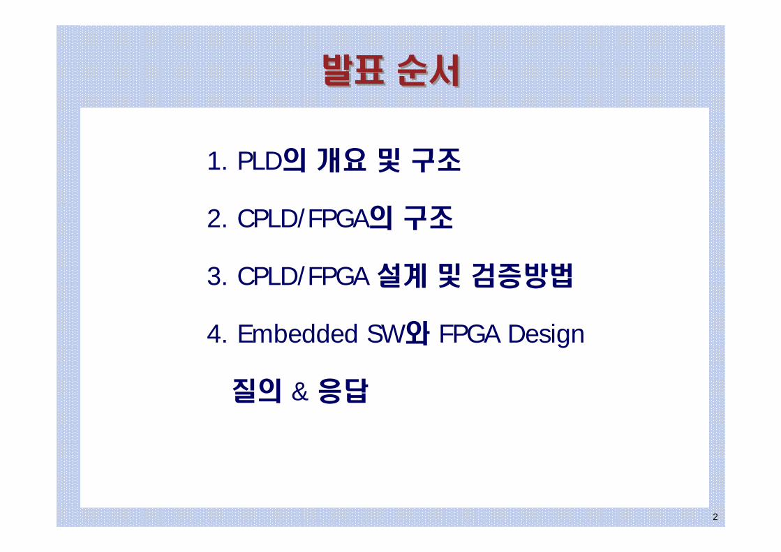
발표 순서발표 순서
1. PLD의 개요 및 구조
2. CPLD/FPGA의 구조
3. CPLD/FPGA 설계 및 검증방법
4. Embedded SW와 FPGA Design
질의 & 응답
3
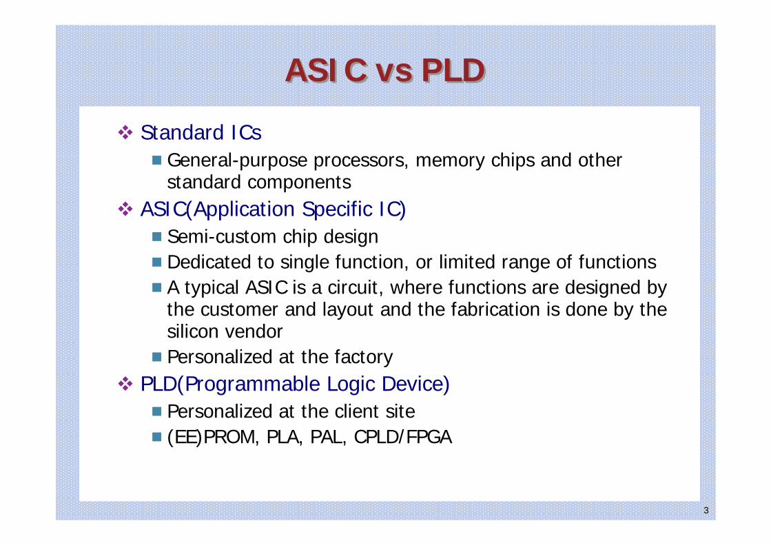
ASIC vs PLDASIC vs PLD
Standard ICsGeneral-purpose processors, memory chips and other standard components
ASIC(Application Specific IC)Semi-custom chip designDedicated to single function, or limited range of functionsA typical ASIC is a circuit, where functions are designed by the customer and layout and the fabrication is done by the silicon vendorPersonalized at the factory
PLD(Programmable Logic Device)Personalized at the client site(EE)PROM, PLA, PAL, CPLD/FPGA
4
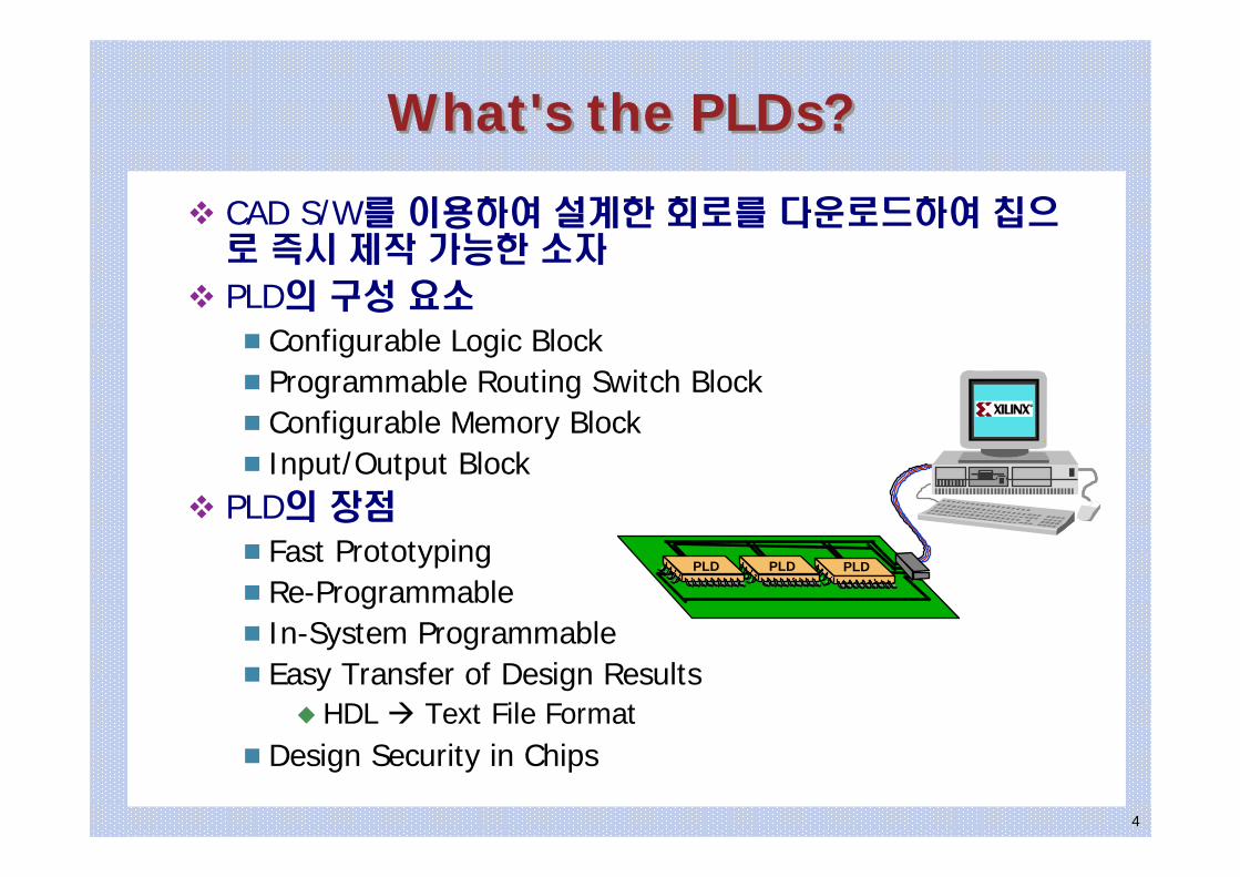
What's the PLDs?What's the PLDs?
CAD S/W를 이용하여 설계한 회로를 다운로드하여 칩으로 즉시 제작 가능한 소자
PLD의 구성 요소
Configurable Logic Block Programmable Routing Switch BlockConfigurable Memory BlockInput/Output Block
PLD의 장점
Fast Prototyping Re-Programmable In-System Programmable Easy Transfer of Design Results
HDL Text File Format Design Security in Chips
PLDPLDPLD
5
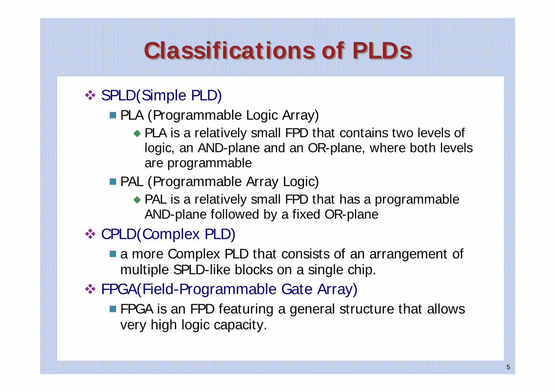
Classifications of PLDsClassifications of PLDs
SPLD(Simple PLD)PLA (Programmable Logic Array)
PLA is a relatively small FPD that contains two levels of logic, an AND-plane and an OR-plane, where both levels are programmable
PAL (Programmable Array Logic)PAL is a relatively small FPD that has a programmable AND-plane followed by a fixed OR-plane
CPLD(Complex PLD)a more Complex PLD that consists of an arrangement of multiple SPLD-like blocks on a single chip.
FPGA(Field-Programmable Gate Array)FPGA is an FPD featuring a general structure that allows very high logic capacity.
6
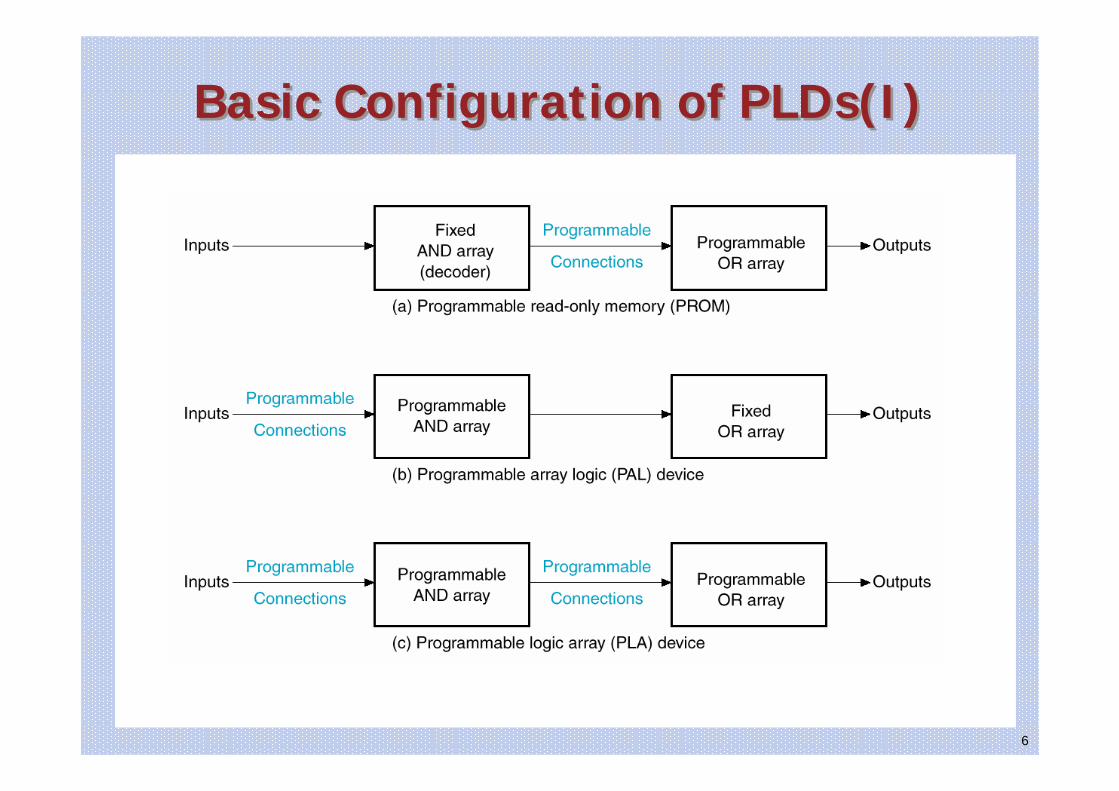
Basic Configuration of PLDs(I)Basic Configuration of PLDs(I)
7
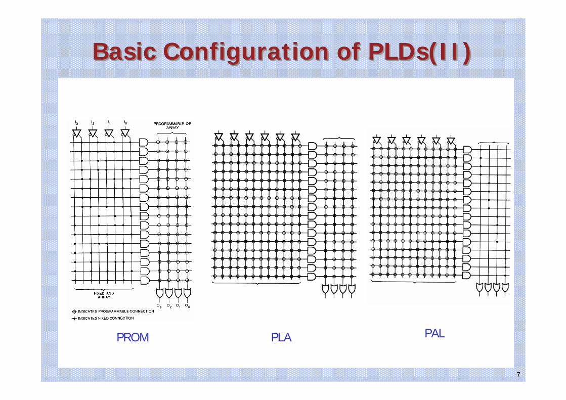
Basic Configuration of PLDs(II)Basic Configuration of PLDs(II)
PROM PALPLA
8
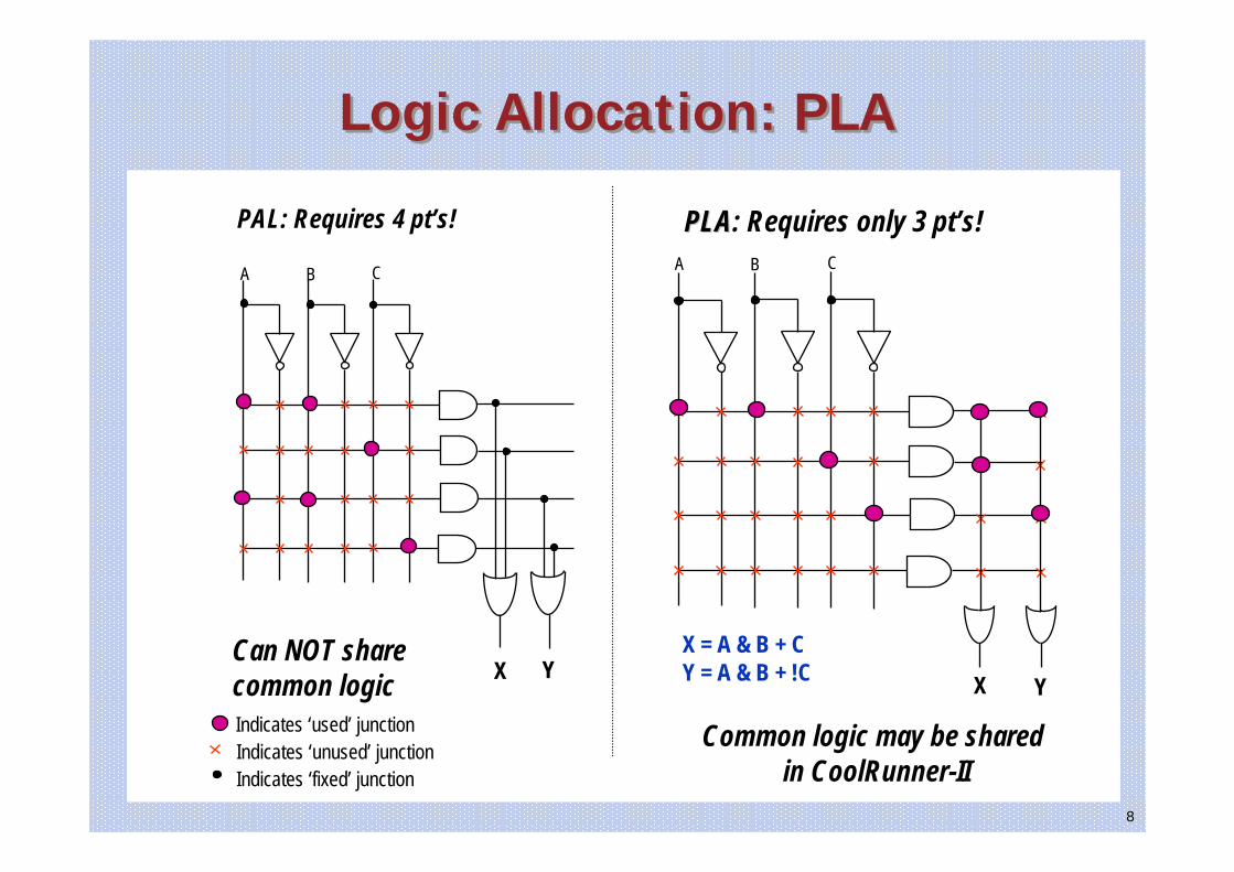
Logic Allocation: PLALogic Allocation: PLA
Common logic may be shared in CoolRunner-II
X = A & B + CY = A & B + !C
PLAPLA: Requires only 3 pt’s!B CA
X Y
B CA
X YCan NOT share common logic
PAL: Requires 4 pt’s!
Indicates ‘unused’ junctionIndicates ‘fixed’ junction
Indicates ‘used’ junction
9
PAL-likeblock
PAL-likeblock
PAL-likeblock
PAL-likeblock
I/O block
I/O block
I/O block
I/O block
Programmable interconnect
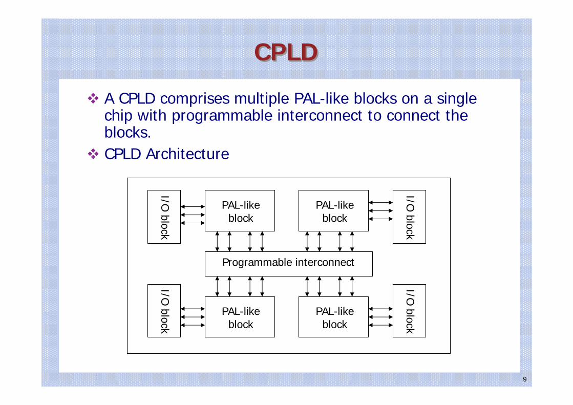
CPLDCPLD
A CPLD comprises multiple PAL-like blocks on a singlechip with programmable interconnect to connect the blocks.CPLD Architecture
10
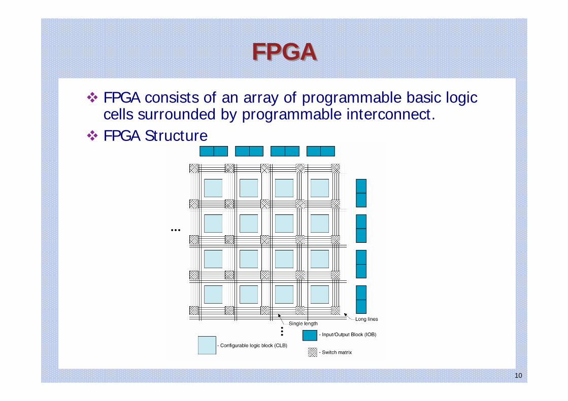
FPGAFPGA
FPGA consists of an array of programmable basic logic cells surrounded by programmable interconnect.FPGA Structure
11
I/O 패드
프로
그램
회로
논리모듈
프로그램 회로
FPGA 구조
프로
그램
회로
프로그램 회로
스위치 매트릭스
배선 채널
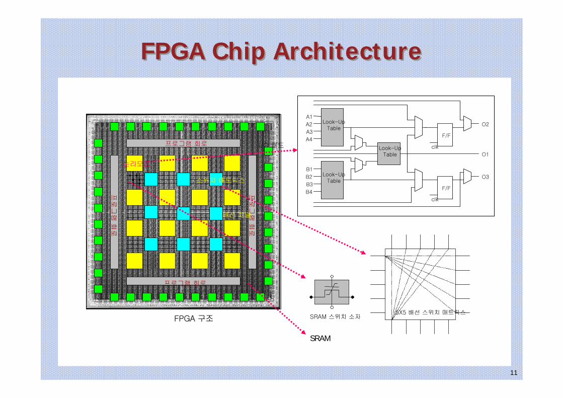
FPGA Chip ArchitectureFPGA Chip Architecture
Look-UpTable
A1
A2
A3
A4
Look-UpTable
B1
B2
B3
B4
Look-UpTable
F/F
clk
F/F
clk
O2
O1
O3
5X5 배선 스위치 매트릭스SRAM 스위치 소자
SRAM
12
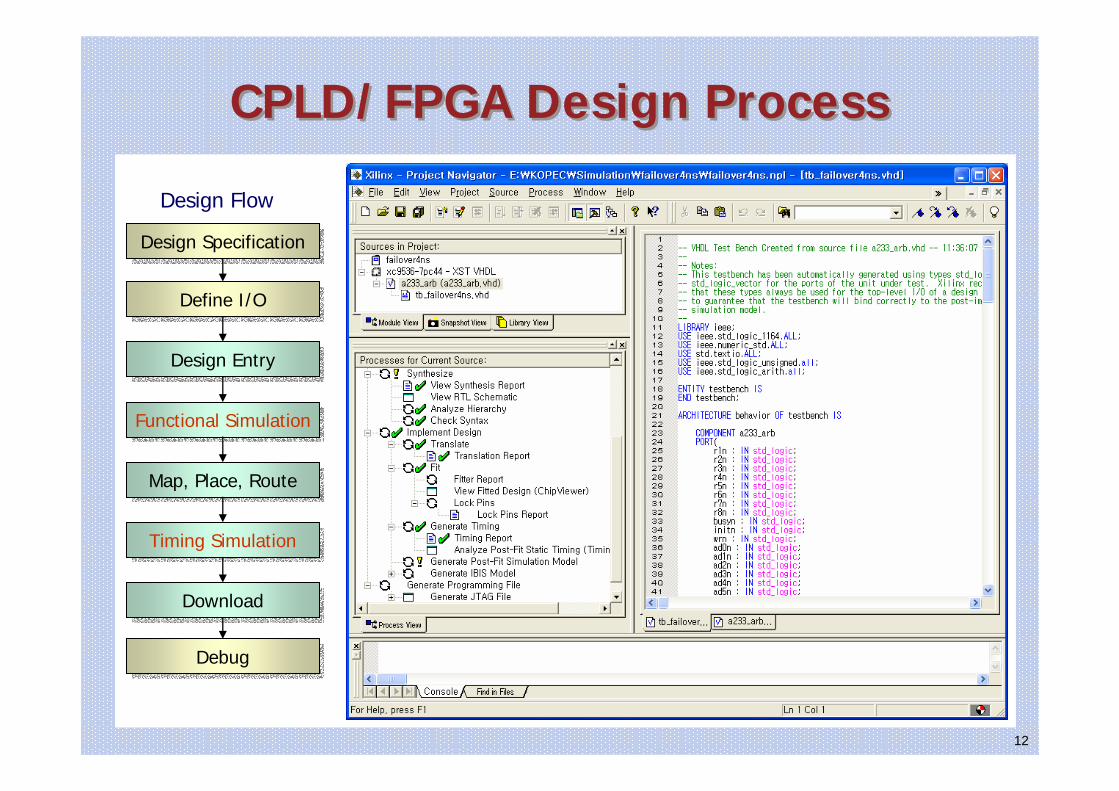
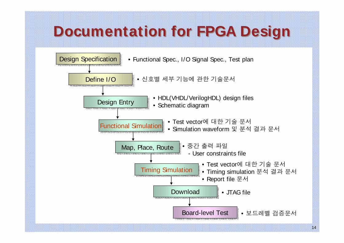
CPLD/FPGA Design ProcessCPLD/FPGA Design Process
Design SpecificationDesign Specification
Define I/ODefine I/O
Design EntryDesign Entry
Functional SimulationFunctional Simulation
Map, Place, RouteMap, Place, Route
Timing SimulationTiming Simulation
DownloadDownload
DebugDebug
Design Flow
13
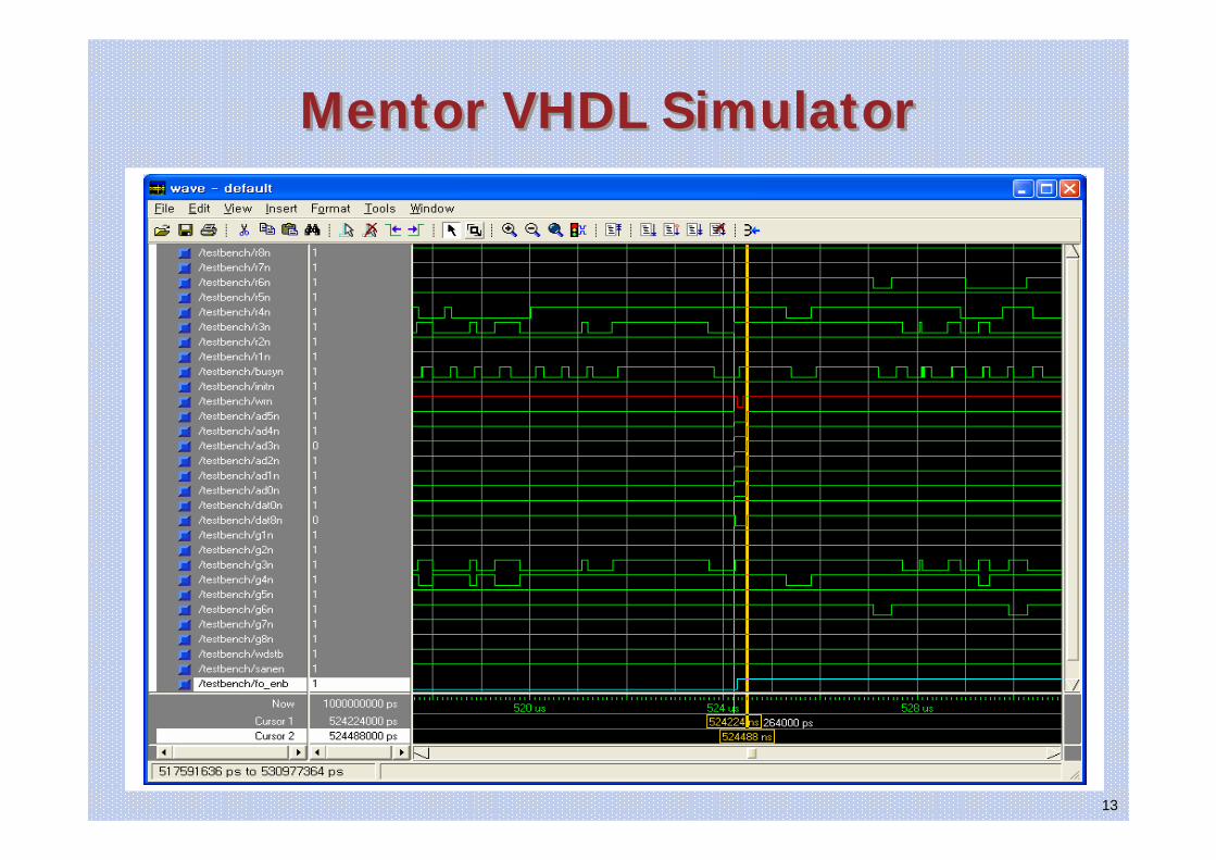
Mentor VHDL SimulatorMentor VHDL Simulator
14
Documentation for FPGA DesignDocumentation for FPGA Design
Design SpecificationDesign Specification
Define I/ODefine I/O
Design EntryDesign Entry
Functional SimulationFunctional Simulation
Map, Place, RouteMap, Place, Route
Timing SimulationTiming Simulation
DownloadDownload
Board-level TestBoard-level Test
• 신호별 세부 기능에 관한 기술문서
• HDL(VHDL/VerilogHDL) design files• Schematic diagram
• Test vector에 대한 기술 문서• Simulation waveform 및 분석 결과 문서
• Test vector에 대한 기술 문서• Timing simulation 분석 결과 문서• Report file 문서
• JTAG file
• 보드레벨 검증문서
• 중간 출력 파일- User constraints file
• Functional Spec., I/O Signal Spec., Test plan
15
CPLD/FPGA 설계 문서화CPLD/FPGA 설계 문서화
CPLD/FPGA 설계 및 검증에 관한 문서화 내용
CPLD/FPGA 설계 방법 및 설계 과정
설계환경(HW, SW), 구체적인 설계 과정
CPLD/FPGA 디바이스 및 내부구조
디바이스선택의 타당성 검토 문서
CPLD/FPGA 설계에 대한 검증 방법론
설계에 대한 Functional/Timing Simulation Simulation Waveform 및 결과 분석서
설계 단계별 중간 생성 자료(파일) 분석서
User Constraints Files검증에 필요한 테스트 시나리오 및 테스트 벡터 집합
보드레벨 검증 문서
검증 환경, 실측 입출력 신호파형, 검증결과 분석서
16
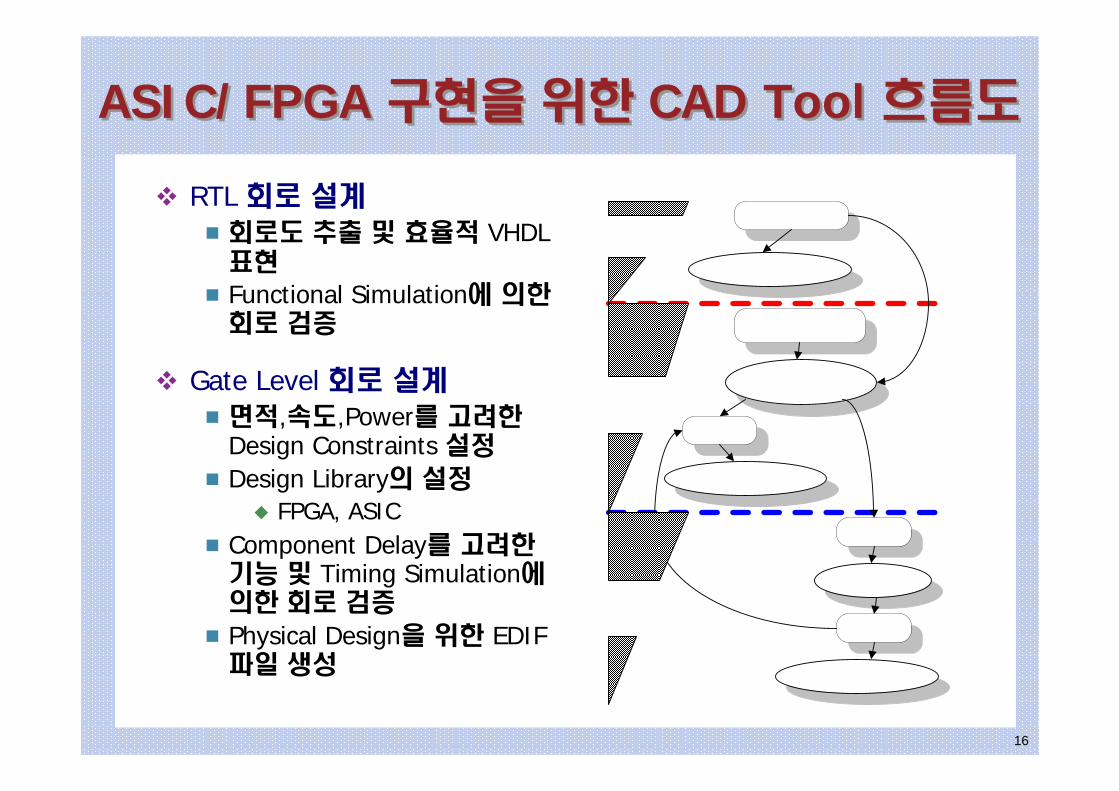
ASIC/FPGA 구현을 위한 CAD Tool 흐름도ASIC/FPGA 구현을 위한 CAD Tool 흐름도
RTL 회로 설계회로도 추출 및 효율적 VHDL 표현
Functional Simulation에 의한회로 검증
Gate Level 회로 설계면적,속도,Power를 고려한Design Constraints 설정
Design Library의 설정FPGA, ASIC
Component Delay를 고려한기능 및 Timing Simulation에의한 회로 검증
Physical Design을 위한 EDIF 파일 생성
17
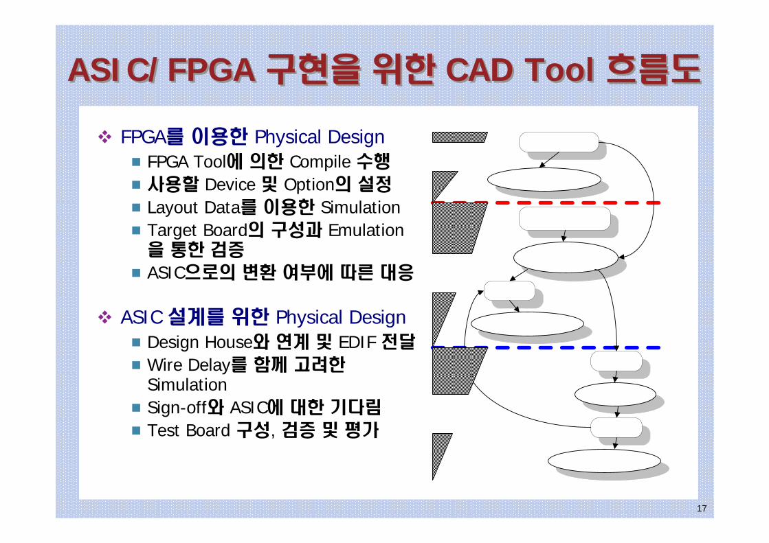
ASIC/FPGA 구현을 위한 CAD Tool 흐름도ASIC/FPGA 구현을 위한 CAD Tool 흐름도
FPGA를 이용한 Physical DesignFPGA Tool에 의한 Compile 수행
사용할 Device 및 Option의 설정
Layout Data를 이용한 SimulationTarget Board의 구성과 Emulation을 통한 검증
ASIC으로의 변환 여부에 따른 대응
ASIC 설계를 위한 Physical Design Design House와 연계 및 EDIF 전달
Wire Delay를 함께 고려한SimulationSign-off와 ASIC에 대한 기다림
Test Board 구성, 검증 및 평가
18
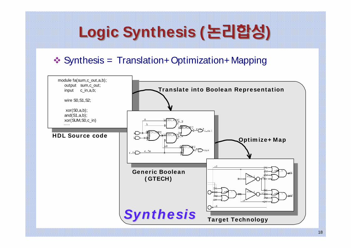
Logic Synthesis (논리합성)Logic Synthesis (논리합성)
Synthesis = Translation+Optimization+Mapping
module fa(sum,c_out,a,b);output sum,c_out;input c_in,a,b;
wire S0,S1,S2;
xor(S0,a,b);and(S1,a,b);xor(SUM,S0,c_in).....
HDL Source code
Generic Boolean(GTECH)
Target Technology
Translate into Boolean Representation
Optimize+Map
SynthesisSynthesis
19
Why HDL?Why HDL?
HDL is for writing models of a systemGrowing complexity of designs
Reasons for modelingRequirements specificationDocumentationTesting using simulationFormal verificationSynthesis
GoalMost reliable design process, with minimum cost and timeAvoid design errors before fabrication
20
Two Major HDLsTwo Major HDLs
Verilog and VHDL
Both are programming languagesText-based, easier to create a design over schematic entry/capture
Verilog is Similar to CVHDL is closer to ADA
Differences to regular programming languagesRegular programming is inherently sequentialHDLs have concurrency (parallel execution) and timingHDLs have constructs to describe hardware
21
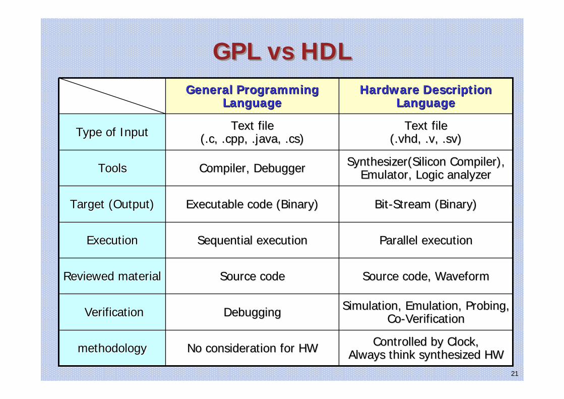
GPL vs HDLGPL vs HDL
Source code, WaveformSource code, WaveformSource codeSource codeReviewed materialReviewed material
Text fileText file(.vhd, .v, .(.vhd, .v, .svsv))
Text fileText file(.c, .(.c, .cppcpp, .java, ., .java, .cscs))Type of InputType of Input
Controlled by Clock,Controlled by Clock,Always think synthesized HWAlways think synthesized HWNo consideration for HWNo consideration for HWmethodology methodology
Simulation, Emulation, Probing, Simulation, Emulation, Probing, CoCo--VerificationVerificationDebuggingDebuggingVerificationVerification
Parallel executionParallel executionSequential executionSequential executionExecutionExecution
BitBit--Stream (Binary)Stream (Binary)Executable code (Binary)Executable code (Binary)Target (Output)Target (Output)
Synthesizer(SiliconSynthesizer(Silicon Compiler),Compiler),Emulator, Logic analyzerEmulator, Logic analyzerCompiler, DebuggerCompiler, DebuggerToolsTools
Hardware Description Hardware Description LanguageLanguage
General Programming General Programming LanguageLanguage
22
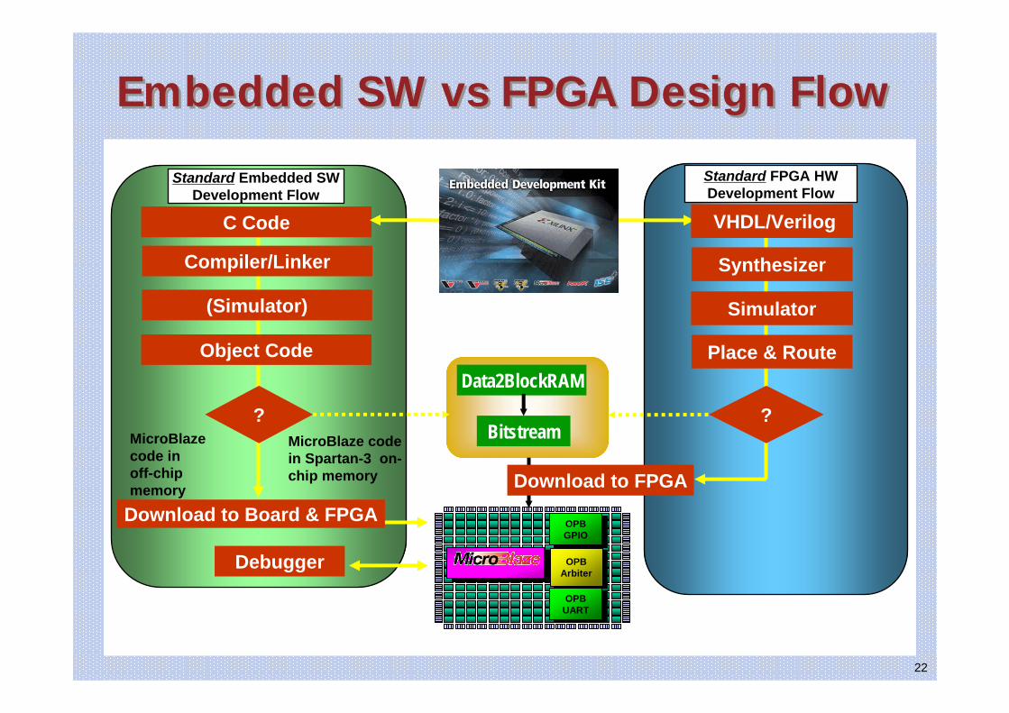
Compiler/Linker
(Simulator)
C Code
Debugger
Data2BlockRAM
Bitstream
Standard Embedded SWDevelopment Flow
Standard FPGA HWDevelopment Flow
Synthesizer
Place & Route
Simulator
VHDL/Verilog
MicroBlaze code in Spartan-3 on-chip memory
?MicroBlazecode in off-chip memory
?
Download to Board & FPGA
Download to FPGA
Embedded SW vs FPGA Design Flow Embedded SW vs FPGA Design Flow
Object Code
OPBUART
OPBArbiter
OPBGPIO
Embedded Development Kit
23
Hardware and Software Co-DesignHardware and Software Co-Design
Approach to develop Traditional SystemsGeneric HardwareSoftware with Relaxed ResourceHW and SW are separated designed.
Approach to develop Embedded SystemsSOFTWARE which is planned to run with resource constraints.HARDWARE which is optimized and specialized to run the software
HW and SW are co-designed.Unified Design Process
24
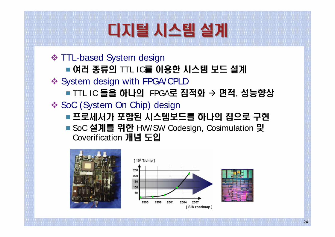
디지털 시스템 설계디지털 시스템 설계
TTL-based System design여러 종류의 TTL IC를 이용한 시스템 보드 설계
System design with FPGA/CPLDTTL IC 들을 하나의 FPGA로 집적화 면적, 성능향상
SoC (System On Chip) design프로세서가 포함된 시스템보드를 하나의 칩으로 구현
SoC 설계를 위한 HW/SW Codesign, Cosimulation 및Coverification 개념 도입
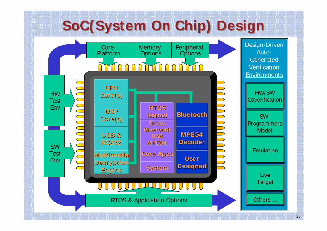
25
SoC(System On Chip) DesignSoC(System On Chip) DesignCore
PlatformMemory Options
Peripheral Options
Design-DrivenAuto-
GeneratedVerification
Environments
RTOS & Application Options
HWTestEnv
HW/SWCoverification
SW Programmers
Model
Emulation
LiveTarget
Others ...
SWTestEnv
BluetoothBluetooth
MPEG4MPEG4DecoderDecoder
UserUserDesignedDesigned
USB &USB &RS232RS232
MultimediaMultimediaDecryptionDecryption
EngineEngine
CPUCPUCore(s)Core(s)
DSPDSPCore(s)Core(s) FlashFlash
SRAMSRAM
DRAMDRAM
RTOSRTOSKernelKernelDriversDrivers
BluetoothBluetoothUSBUSB
MPEG4MPEG4
Core AppsCore Apps
SystemSystem

질의 & 응답질의 & 응답