radiofrequency plasma sources for semiconductor …ffchen/publs/chen213p.pdf · 6 6 radiofrequency...
TRANSCRIPT
1
2
3
4
5
6
7
8
9
10
11
12
13
14
15
16
17
18
19
20
21
22
23
24
25
26
27
28
29
30
31
32
33
34
35
36
37
38
39
40
41
42
43
44
45
������������ ���� ��� ������
������� �������������
���� �����������
����� ��������������� ��������� �
��� �����������
��������� � � � � � � � � � � � � � � � � � � � � � � � � � � � � � � � � � � �
���������������� � � � � � � � � � � � � � � � � � � � � � � � � � � � �
6
Radiofrequency Plasma Sources for Semiconductor ProcessingFrancis F. Chen
6.1
Introduction
In the etching anddeposition steps in the production of semiconductor chips, plasma
processing is required for three main reasons. First, electrons are used to dissociate
the input gas into atoms. Second, the etch rate is greatly enhanced by ion bombard-
ment, which breaks the bonds in the first fewmonolayers of the surface, allowing the
etchant atoms, usually Cl or F, to combine with substrate atoms to form volatile
molecules. And third, most importantly, the electric field of the plasma sheath
straightens the orbits of the bombarding ions so that the etching is anisotropic,
allowing the creation of features approaching nanometer dimensions.
The plasma sources used in the semiconductor industry were originally developed
by trial and error, with little basic understanding of how they work. To achieve this
understanding, many challenging physics problems had to be solved. This chapter is
an introduction to the science of radiofrequency (rf ) plasma sources, which are by far
themost common. Sources operating at zero or other frequencies, such as 2.45GHz
microwaves, lie outside our scope. Most rf sources use the 13.56MHz industrial
standard frequency. Among these, there are threemain types: (1) capacitively coupled
plasmas or CCPs, also called reactive ion etchers (RIEs); (2) inductively coupled
plasmas (ICPs), also called transformer coupled plasmas (TCPs); and (3) helicon
wave sources, which are new and can be called HWSs.
6.2
Capacitively Coupled Plasmas
The principal parts of a CCPare shown schematically in Fig. 6.1. In its simplest form,
the rfvoltageisappliedacrosstwoparallelmetalplates,generatinganoscillatingelectric
field between them. This field accelerates electrons, heating their thermal distribution
to have enough high-energy electrons in the tail to cause an ionization avalanche. The
densityrisestoanequilibriumvaluesetbytherfpowerandthedensityoftheneutralgas.
The silicon wafer to be processed is attached to the normally grounded electrode by an
Advanced Plasma Technology. Edited by Riccardo d’Agostino, Pietro Favia, Yoshinobu Kawai, Hideo Ikegami,Noriyoshi Sato, and Farzaneh Arefi-KhonsariCopyright � 2007 WILEY-VCH Verlag GmbH & Co. KGaA, WeinheimISBN: 978-3-527-40591-6
99
1
2
3
4
5
6
7
8
9
10
11
12
13
14
15
16
17
18
19
20
21
22
23
24
25
26
27
28
29
30
31
32
33
34
35
36
37
38
39
40
41
42
43
44
45
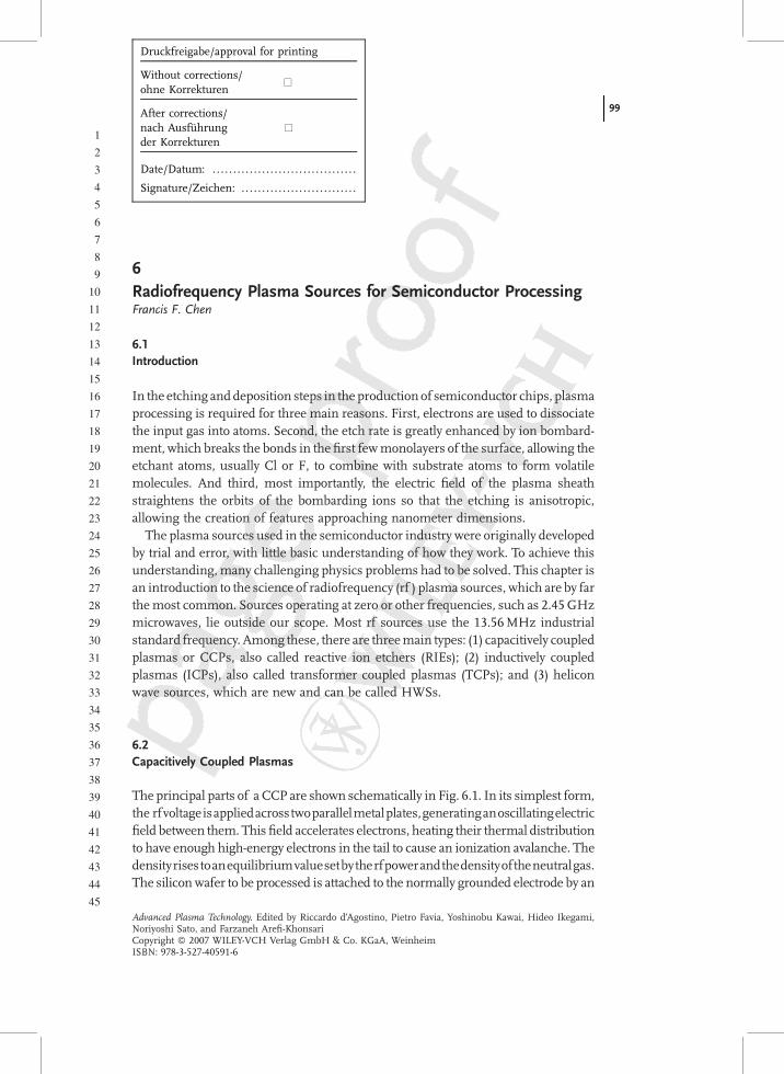
electrostatic chuck.The latteruseselectrostatic charges tohold thewafer incontactwith
the electrode and also provides small channels for flow of helium to cool the wafer. To
keep theplasmaneutral, sheathsautomatically formnext to theelectrodesprovidingan
electric field (E-field) perpendicular to their surfaces. The potential drop in the sheath
repels the fast-moving electrons so that they can escape no faster than the ions. At the
same time, the sheath E-field accelerates the ions to bombard the surface and perform
the beneficial functions mentioned above.
The sheath drop is of order 5KTe, where Te is the electron temperature. For a 3 eV
plasma, the ion energy is of order 15 eV. Since rf voltage is applied, the sheath drop
and sheath thickness will oscillate at the rf frequency. Even if one electrode is
grounded, the plasma potential will oscillate so as to make the two sheaths identical,
but out of phase. The sheath oscillationwill affect the ion energy distribution function
(IEDF), depending on the transit time of the ions through the sheath. At low
pressures, the IEDF at the wafer surface tends to be bimodal, with peaks at the
maximum and minimum sheath drops, since a sine wave changes slowly at its
extrema. CCPs are relatively inefficient ionizers and work best at high pressures and
low densities. The sheath thickness, therefore, can become measurably large, of
order millimeters. If the ion mean free path (mfp) for collisions with neutrals is
smaller than the sheath thickness, the IEDF will be pressure-broadened. There are
also other heating mechanisms. In resonant heating, some fast electrons can travel
between the two sheaths without colliding, and those with just the right velocity can
catch each sheath in its expanding phase, thus getting accelerated at each bounce.
Such effects in classic CCPs are further described in textbooks [1,2].
6.2.1
Dual-Frequency CCPs
If ion bombardment energies larger than the normal sheath drop are desired, one
can apply a second rf source, a bias oscillator, to the electrode bearing the substrate.
Fig. 6.1 Schematic of a capacitive discharge.
100 6 Radiofrequency Plasma Sources for Semiconductor Processing
1
2
3
4
5
6
7
8
9
10
11
12
13
14
15
16
17
18
19
20
21
22
23
24
25
26
27
28
29
30
31
32
33
34
35
36
37
38
39
40
41
42
43
44
45
This is usually at a lower frequency, which has a larger effect on themassive ions. The
time-averaged sheath drop will then increase by the following rectification effect.
When the electrode is driven positive, a large electron current flows to it through the
lowered Coulomb barrier, but when the electrode goes negative, there is no
corresponding ion current because the ions are much slower. Unless the electrode
emits electrons, it will accumulate a negative charge. Applying a large rf bias voltage
to the substrate will, therefore, increase the dc (direct current) sheath drop even
though the bias voltage is ac. It is not generally possible to apply a dc voltage directly,
since parts of the wafer may be non-conducting. An rf voltage, however, will be
conveyed capacitively through these insulating layers.
Bias power supplies have been used for many years, but recently the dual-
frequency concept has found an important application in CCPs with extremely thin
gaps. These new devices perform well in oxide etch; that is, in the etching of SiO2, a
difficult process since Si intrinsically etches faster than its oxide. The reason that thin-
gap CCPs work is not yet understood, but interest in them has spawned computa-
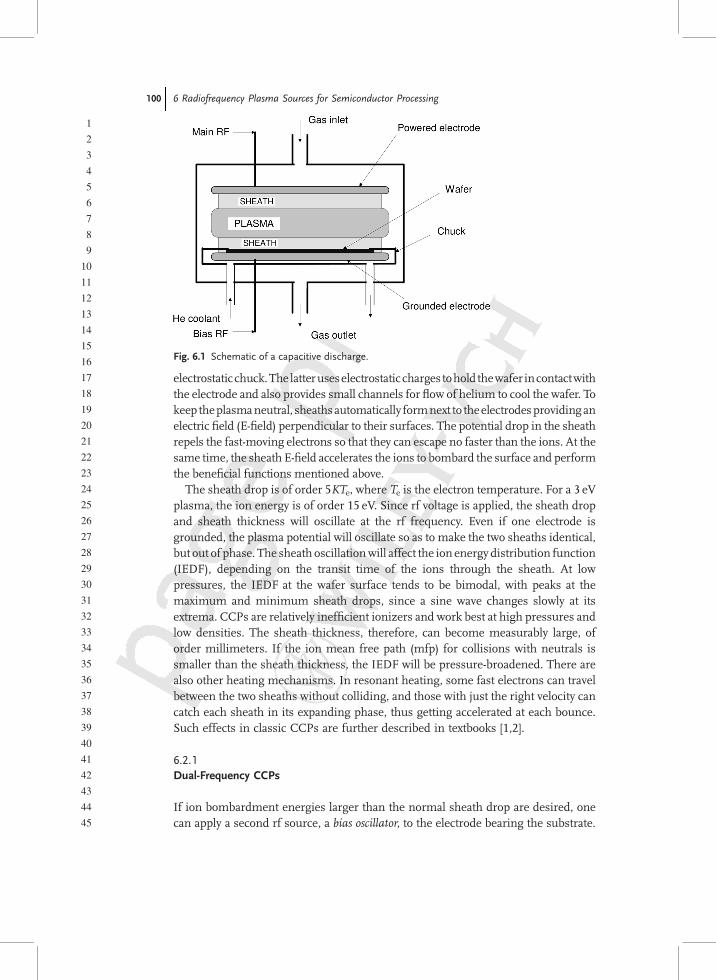
tional studieswhichhave advanced the science ofCCPs in general. Figure 6.2 shows a
schematic of this type of source. The electrodes are asymmetric; the wafer-bearing
plate is smaller to enhance the sheath drop there. The high frequency produces the
plasma, and the low frequency controls the ion distribution in the sheath. These
devices are quite different from the original RIEs because they operate at high
pressure (10–100mtorr), and the gaps are very small (1–3 cm). With high rf bias
voltage, the sheaths are quite thick and can occupymost of the volume, leaving only a
small region of quasineutral plasmanear themidplane. In this limit, what happens in
the sheath controls the plasma production. Upon striking the substrate, those
electrons that have penetrated the sheath produce more electrons by secondary
emission. The emitted electrons are then accelerated toward the plasma by the sheath
field. They ionize the neutral gas inside the sheath, since the ionization mfp can be
smaller than the sheath thickness. The avalanche that creates the plasma then starts
in the sheath.
Since the sheaths oscillate at two frequencies and their beats and harmonics, it is
clear that extensive computer simulation is required to model the complicated
Fig. 6.2 Schematic of a thin-gap, dual-frequency CCP.
6.2 Capacitively Coupled Plasmas 101

1
2
3
4
5
6
7
8
9
10
11
12
13
14
15
16
17
18
19
20
21
22
23
24
25
26
27
28
29
30
31
32
33
34
35
36
37
38
39
40
41
42
43
44
45
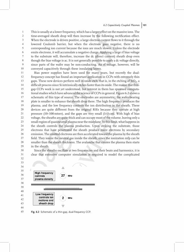
behavior in these collisional sheaths. We quote here just a few results from Lee’s
group at PohangUniversity in South Korea [3,5]. It is well known [1] in CCPs that the
density increases with the square of the frequency. At constant power, therefore, the
density increases, and the Debye length decreases, with frequency. The resulting
change in sheath thickness is clearly demonstrated in Fig. 6.3. The IEDFs and EEDFs
change not only with frequency but also with pressure. The pressure variation of
IEDF is shown in Fig. 6.4, where it is seen that the typical bimodal distribution at low
pressure is smoothed out by collisions at high pressure. Particle-in-cell simulations
are invaluable in understanding complicated plasmas such as these. However, some
aspects, such as why CCPs create less damage to oxide layers in etching, are still
beyond the capabilities of theory. At this point, CCPs have been revived both as
important manufacturing tools and as academically interesting subjects.
Fig. 6.3 Simulation of ion and electron density profiles at various
frequencies [5].
102 6 Radiofrequency Plasma Sources for Semiconductor Processing
1
2
3
4
5
6
7
8
9
10
11
12
13
14
15
16
17
18
19
20
21
22
23
24
25
26
27
28
29
30
31
32
33
34
35
36
37
38
39
40
41
42
43
44
45
6.3
Inductively Coupled Plasmas
6.3.1
General Description
Though simple and inexpensive, the original CCPs had a number of disadvantages,
and a new generation of plasma sources was called for. For instance, the internal
electrodes in CCPs introduced unnecessary impurities into the plasma. Until dual-
frequency CCPs were introduced, there was a lack of control: changing the rf power
changed both the plasma density and the sheath drop, and varying the pressure to do
thiswould also change the chemistry. The highpressures also created a dust problem:
negatively charged particulates of micrometer size or larger would form and be
suspended above the substrate by the electric field, and these would collapse onto the
wafer at plasma turn-off, thus destroying some of the chips. These problems are
overcome in ICPs, which use an external coil (‘‘antenna’’) to induce an electric field
inside the chamber according to Faraday’s law. The most common antenna shapes
are illustrated in Fig. 6.5.
Fig. 6.4 Ion distributions at the substrate for different pressures [3].
6.3 Inductively Coupled Plasmas 103
1
2
3
4
5
6
7
8
9
10
11
12
13
14
15
16
17
18
19
20
21
22
23
24
25
26
27
28
29
30
31
32
33
34
35
36
37
38
39
40
41
42
43
44
45
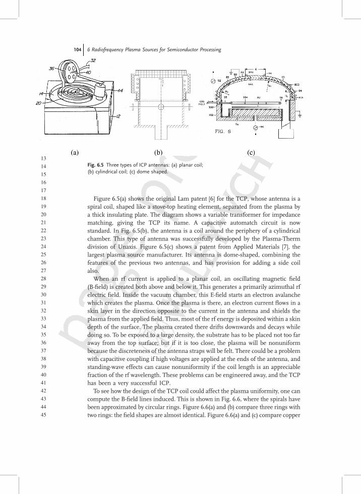
Figure 6.5(a) shows the original Lam patent [6] for the TCP, whose antenna is a
spiral coil, shaped like a stove-top heating element, separated from the plasma by
a thick insulating plate. The diagram shows a variable transformer for impedance
matching, giving the TCP its name. A capacitive automatch circuit is now
standard. In Fig. 6.5(b), the antenna is a coil around the periphery of a cylindrical
chamber. This type of antenna was successfully developed by the Plasma-Therm
division of Unaxis. Figure 6.5(c) shows a patent from Applied Materials [7], the
largest plasma source manufacturer. Its antenna is dome-shaped, combining the
features of the previous two antennas, and has provision for adding a side coil
also.
When an rf current is applied to a planar coil, an oscillating magnetic field
(B-field) is created both above and below it. This generates a primarily azimuthal rf
electric field. Inside the vacuum chamber, this E-field starts an electron avalanche
which creates the plasma. Once the plasma is there, an electron current flows in a
skin layer in the direction opposite to the current in the antenna and shields the
plasma from the applied field. Thus, most of the rf energy is deposited within a skin
depth of the surface. The plasma created there drifts downwards and decays while
doing so. To be exposed to a large density, the substrate has to be placed not too far
away from the top surface; but if it is too close, the plasma will be nonuniform
because the discreteness of the antenna straps will be felt. There could be a problem
with capacitive coupling if high voltages are applied at the ends of the antenna, and
standing-wave effects can cause nonuniformity if the coil length is an appreciable
fraction of the rf wavelength. These problems can be engineered away, and the TCP
has been a very successful ICP.
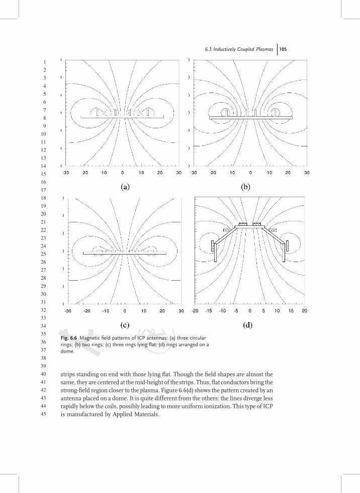
To see how the design of the TCP coil could affect the plasma uniformity, one can
compute the B-field lines induced. This is shown in Fig. 6.6, where the spirals have
been approximated by circular rings. Figure 6.6(a) and (b) compare three rings with
two rings: the field shapes are almost identical. Figure 6.6(a) and (c) compare copper
Fig. 6.5 Three types of ICP antennas: (a) planar coil;
(b) cylindrical coil; (c) dome shaped.
104 6 Radiofrequency Plasma Sources for Semiconductor Processing
1
2
3
4
5
6
7
8
9
10
11
12
13
14
15
16
17
18
19
20
21
22
23
24
25
26
27
28
29
30
31
32
33
34
35
36
37
38
39
40
41
42
43
44
45
strips standing on end with those lying flat. Though the field shapes are almost the
same, they are centered at themid-height of the strips. Thus, flat conductors bring the
strong-field region closer to the plasma. Figure 6.6(d) shows the pattern created by an
antenna placed on a dome. It is quite different from the others; the lines diverge less
rapidly below the coils, possibly leading tomore uniform ionization. This type of ICP
is manufactured by Applied Materials.
Fig. 6.6 Magnetic field patterns of ICP antennas: (a) three circular
rings; (b) two rings; (c) three rings lying flat; (d) rings arranged on a
dome.
6.3 Inductively Coupled Plasmas 105
1
2
3
4
5
6
7
8
9
10
11
12
13
14
15
16
17
18
19
20
21
22
23
24
25
26
27
28
29
30
31
32
33
34
35
36
37
38
39
40
41
42
43
44
45
6.3.2
Anomalous Skin Depth
At first glance, the side-wound antenna of Fig. 6.5(b) should give poor plasma
uniformity. Since the skin depth is of the order of a few centimeters, much less than
the radius of the substrate to be processed, one would expect the density to be high
only near the periphery. Actually, the opposite is true, and parameters can be adjusted
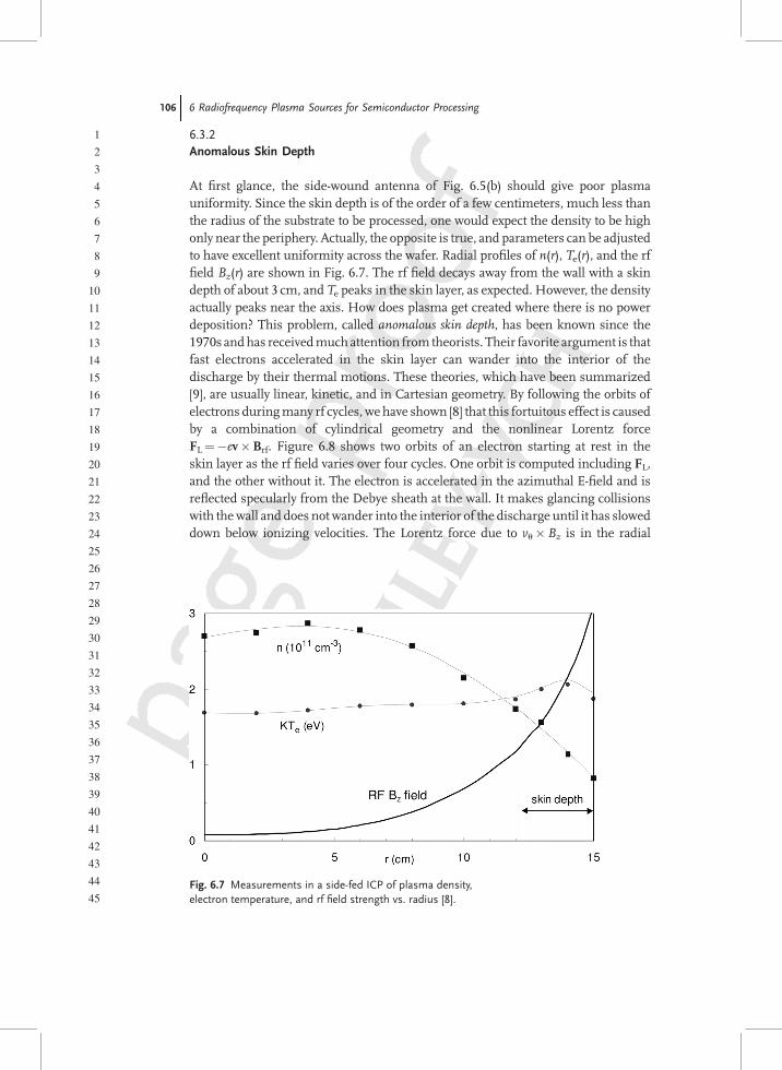
to have excellent uniformity across the wafer. Radial profiles of n(r), Te(r), and the rf
field Bz(r) are shown in Fig. 6.7. The rf field decays away from the wall with a skin
depth of about 3 cm, and Te peaks in the skin layer, as expected. However, the density
actually peaks near the axis. How does plasma get created where there is no power
deposition? This problem, called anomalous skin depth, has been known since the
1970s andhas receivedmuch attention from theorists. Their favorite argument is that
fast electrons accelerated in the skin layer can wander into the interior of the
discharge by their thermal motions. These theories, which have been summarized
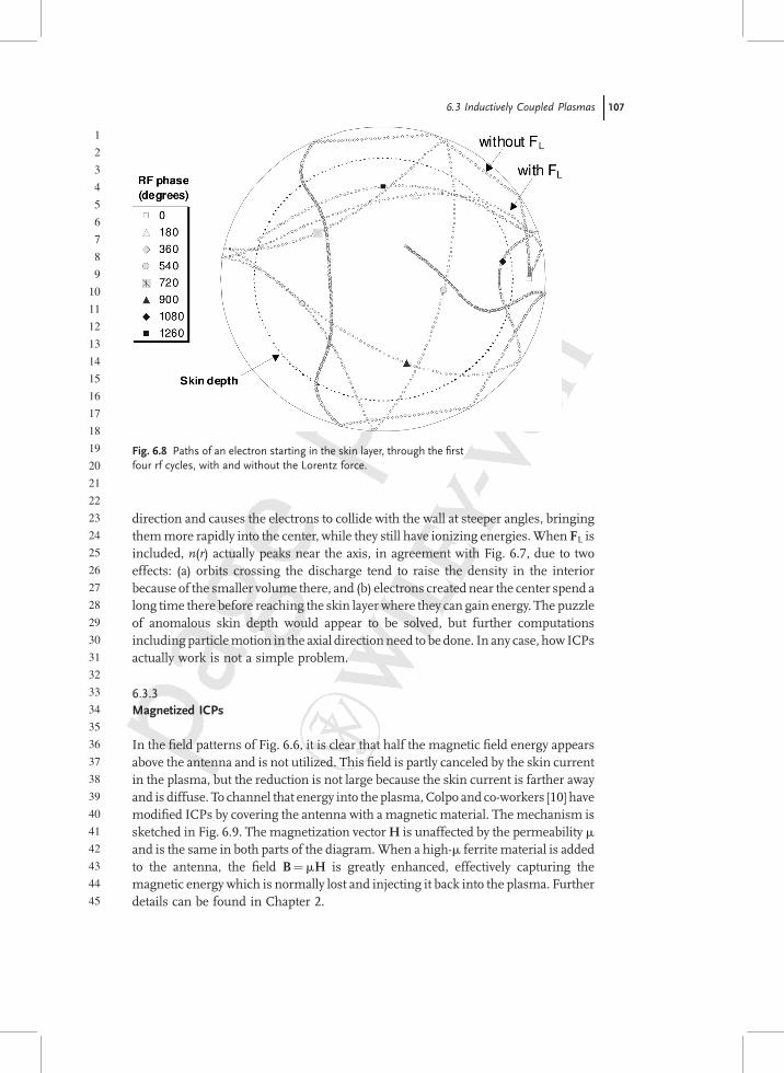
[9], are usually linear, kinetic, and in Cartesian geometry. By following the orbits of
electrons duringmany rf cycles, we have shown [8] that this fortuitous effect is caused
by a combination of cylindrical geometry and the nonlinear Lorentz force
FL¼�ev�Brf. Figure 6.8 shows two orbits of an electron starting at rest in the
skin layer as the rf field varies over four cycles. One orbit is computed including FL,
and the other without it. The electron is accelerated in the azimuthal E-field and is
reflected specularly from the Debye sheath at the wall. It makes glancing collisions
with thewall and does not wander into the interior of the discharge until it has slowed
down below ionizing velocities. The Lorentz force due to vu�Bz is in the radial
Fig. 6.7 Measurements in a side-fed ICP of plasma density,
electron temperature, and rf field strength vs. radius [8].
106 6 Radiofrequency Plasma Sources for Semiconductor Processing
1
2
3
4
5
6
7
8
9
10
11
12
13
14
15
16
17
18
19
20
21
22
23
24
25
26
27
28
29
30
31
32
33
34
35
36
37
38
39
40
41
42
43
44
45
direction and causes the electrons to collide with the wall at steeper angles, bringing
themmore rapidly into the center, while they still have ionizing energies.When FL is
included, n(r) actually peaks near the axis, in agreement with Fig. 6.7, due to two
effects: (a) orbits crossing the discharge tend to raise the density in the interior
because of the smaller volume there, and (b) electrons created near the center spend a
long time there before reaching the skin layer where they can gain energy. The puzzle
of anomalous skin depth would appear to be solved, but further computations
including particlemotion in the axial directionneed to be done. In any case, how ICPs
actually work is not a simple problem.
6.3.3
Magnetized ICPs
In the field patterns of Fig. 6.6, it is clear that half the magnetic field energy appears
above the antenna and is not utilized. This field is partly canceled by the skin current
in the plasma, but the reduction is not large because the skin current is farther away
and is diffuse. To channel that energy into the plasma, Colpo and co-workers [10] have
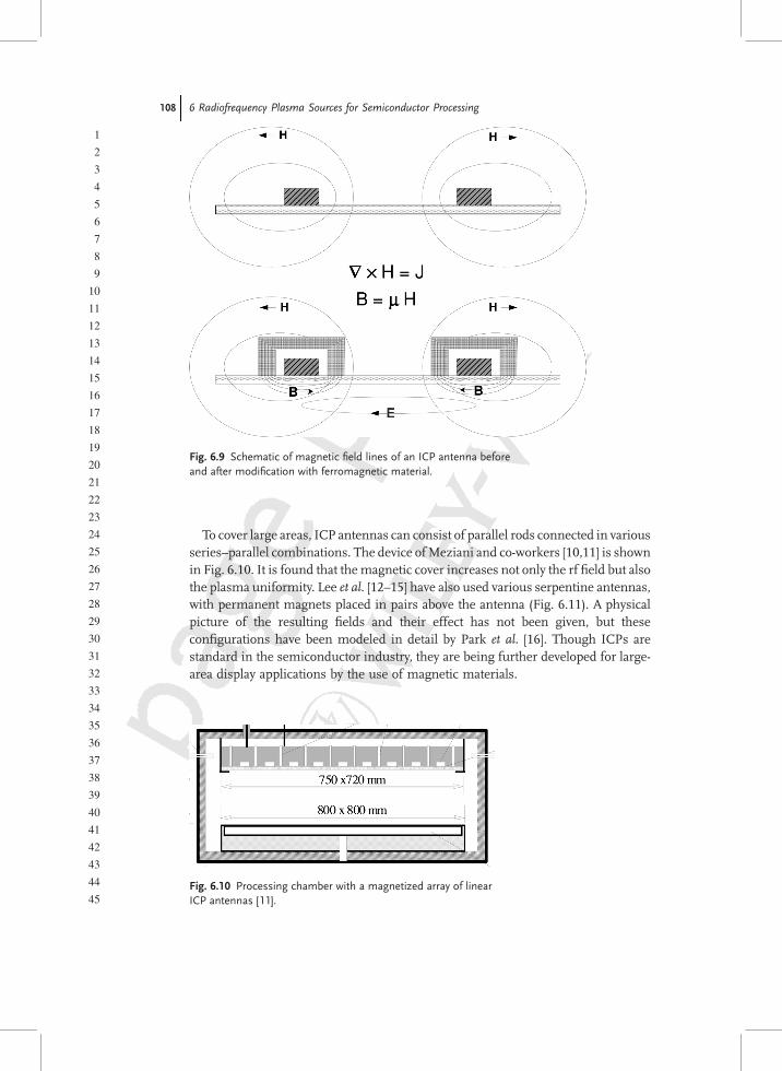
modified ICPs by covering the antenna with a magnetic material. The mechanism is
sketched in Fig. 6.9. The magnetization vectorH is unaffected by the permeability m
and is the same in both parts of the diagram.When a high-m ferrite material is added
to the antenna, the field B¼mH is greatly enhanced, effectively capturing the
magnetic energy which is normally lost and injecting it back into the plasma. Further
details can be found in Chapter 2.
Fig. 6.8 Paths of an electron starting in the skin layer, through the first
four rf cycles, with and without the Lorentz force.
6.3 Inductively Coupled Plasmas 107
1
2
3
4
5
6
7
8
9
10
11
12
13
14
15
16
17
18
19
20
21
22
23
24
25
26
27
28
29
30
31
32
33
34
35
36
37
38
39
40
41
42
43
44
45
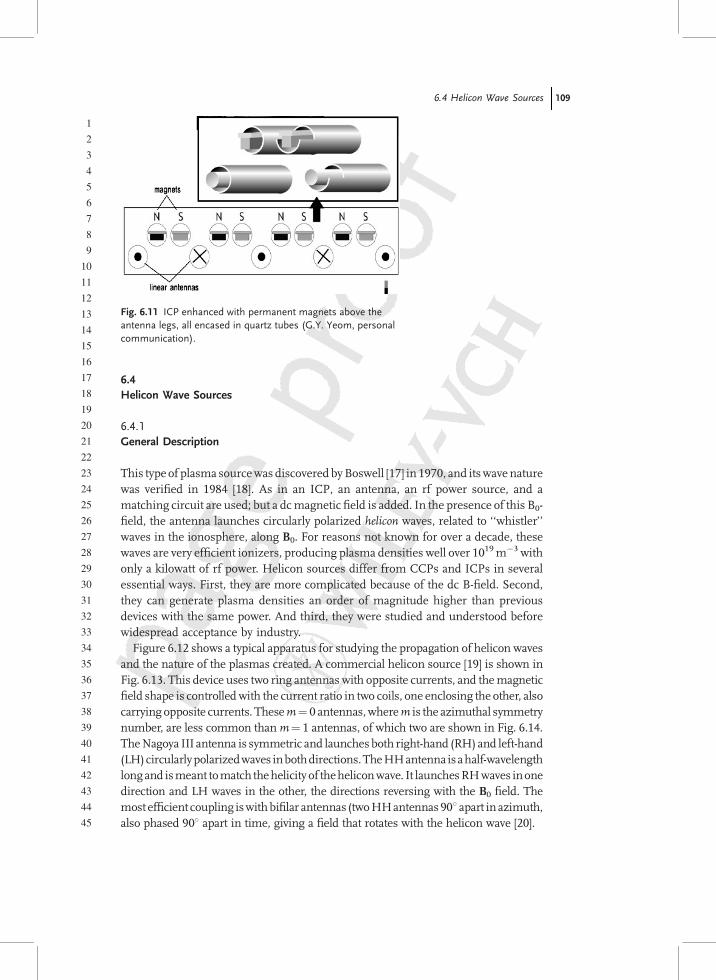
To cover large areas, ICP antennas can consist of parallel rods connected in various
series–parallel combinations. The device ofMeziani and co-workers [10,11] is shown
in Fig. 6.10. It is found that the magnetic cover increases not only the rf field but also
the plasma uniformity. Lee et al. [12–15] have also used various serpentine antennas,with permanent magnets placed in pairs above the antenna (Fig. 6.11). A physical
picture of the resulting fields and their effect has not been given, but these
configurations have been modeled in detail by Park et al. [16]. Though ICPs are
standard in the semiconductor industry, they are being further developed for large-
area display applications by the use of magnetic materials.
Fig. 6.9 Schematic of magnetic field lines of an ICP antenna before
and after modification with ferromagnetic material.
Fig. 6.10 Processing chamber with a magnetized array of linear
ICP antennas [11].
108 6 Radiofrequency Plasma Sources for Semiconductor Processing
1
2
3
4
5
6
7
8
9
10
11
12
13
14
15
16
17
18
19
20
21
22
23
24
25
26
27
28
29
30
31
32
33
34
35
36
37
38
39
40
41
42
43
44
45
6.4
Helicon Wave Sources
6.4.1
General Description
This type of plasma sourcewas discovered byBoswell [17] in 1970, and itswave nature
was verified in 1984 [18]. As in an ICP, an antenna, an rf power source, and a
matching circuit are used; but a dcmagnetic field is added. In the presence of this B0-
field, the antenna launches circularly polarized helicon waves, related to ‘‘whistler’’
waves in the ionosphere, along B0. For reasons not known for over a decade, these
waves are very efficient ionizers, producing plasma densities well over 1019m�3 with
only a kilowatt of rf power. Helicon sources differ from CCPs and ICPs in several
essential ways. First, they are more complicated because of the dc B-field. Second,
they can generate plasma densities an order of magnitude higher than previous
devices with the same power. And third, they were studied and understood before
widespread acceptance by industry.
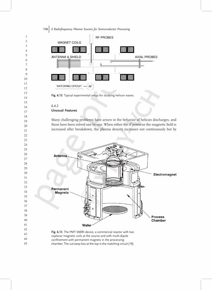
Figure 6.12 shows a typical apparatus for studying the propagation of helicon waves
and the nature of the plasmas created. A commercial helicon source [19] is shown in
Fig. 6.13. This device uses two ring antennas with opposite currents, and themagnetic
field shape is controlledwith the current ratio in two coils, one enclosing the other, also
carrying opposite currents. Thesem¼ 0 antennas,wherem is the azimuthal symmetry
number, are less common thanm¼ 1 antennas, of which two are shown in Fig. 6.14.
TheNagoya III antenna is symmetric and launches both right-hand (RH) and left-hand
(LH)circularlypolarizedwaves inbothdirections.TheHHantenna isahalf-wavelength
longand ismeant tomatch thehelicity of theheliconwave. It launchesRHwaves inone
direction and LH waves in the other, the directions reversing with the B0 field. The
most efficient coupling iswithbifilar antennas (twoHHantennas908 apart inazimuth,
also phased 908 apart in time, giving a field that rotates with the helicon wave [20].
Fig. 6.11 ICP enhanced with permanent magnets above the
antenna legs, all encased in quartz tubes (G.Y. Yeom, personal
communication).
6.4 Helicon Wave Sources 109
1
2
3
4
5
6
7
8
9
10
11
12
13
14
15
16
17
18
19
20
21
22
23
24
25
26
27
28
29
30
31
32
33
34
35
36
37
38
39
40
41
42
43
44
45
6.4.2
Unusual Features
Many challenging problems have arisen in the behavior of helicon discharges, and
these have been solved one by one. When either the rf power or the magnetic field is
increased after breakdown, the plasma density increases not continuously but by
Fig. 6.12 Typical experimental setup for studying helicon waves.
Fig. 6.13 The PMT MØRI device, a commercial reactor with two
coplanar magnetic coils at the source and with multi-dipole
confinement with permanent magnets in the processing
chamber. The cut-away box at the top is the matching circuit [19].
110 6 Radiofrequency Plasma Sources for Semiconductor Processing
1
2
3
4
5
6
7
8
9
10
11
12
13
14
15
16
17
18
19
20
21
22
23
24
25
26
27
28
29
30
31
32
33
34
35
36
37
38
39
40
41
42
43
44
45
discrete jumps. At low power, the coupling is capacitive, and the discharge is a CCP.
As the power is raised, the plasma jumps into ICP operation as inductive coupling
takes hold. When the conditions for propagation of helicon waves are met, there is a
large jump into the lowest heliconmode and the peak density can be 20 times higher
than in ICP mode. There may be further jumps into higher-order radial modes. A
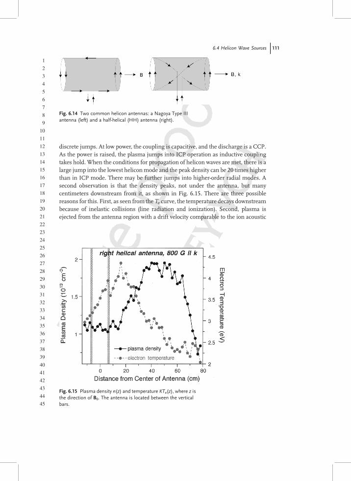
second observation is that the density peaks, not under the antenna, but many
centimeters downstream from it, as shown in Fig. 6.15. There are three possible
reasons for this. First, as seen from theTe curve, the temperature decays downstream
because of inelastic collisions (line radiation and ionization). Second, plasma is
ejected from the antenna region with a drift velocity comparable to the ion acoustic
Fig. 6.14 Two common helicon antennas: a Nagoya Type III
antenna (left) and a half-helical (HH) antenna (right).
Fig. 6.15 Plasma density n(z) and temperature KTe(z), where z is
the direction of B0. The antenna is located between the vertical
bars.
6.4 Helicon Wave Sources 111
1
2
3
4
5
6
7
8
9
10
11
12
13
14
15
16
17
18
19
20
21
22
23
24
25
26
27
28
29
30
31
32
33
34
35
36
37
38
39
40
41
42
43
44
45
velocity cs. This is just the Bohm criterion for sheath formation. There is no sheath
here, but the criterion still has to bemet if there are very few ions created downstream
which can travel back to the antenna. Finally, there may actually be a little ionization
downstream due to parametric instabilities, an effect recently verified in experiment.
The result is that the helicon discharge is an ideal ‘‘remote’’ source, in which the
substrate can be located in a desirable region of high density and low Te, far from the
high fields near the antenna.
A second, more important, problem is: What causes the high ionization efficiency
of HWSs compared with ICPs? There is no difference in confinement, since the
B-fields of 50–1000Gs (5–100mT) normally used are not sufficient to confine
the ions, and the electrons are not confined axially. Hence, the difference must
be in the way in which rf energy is absorbed. In ICPs, collisional absorption converts
the electron energy gained in the skin layer into a general rise in KTe, and the tail of
this Maxwellian distribution does the ionization. Since helicon waves travel along B0
with velocities comparable to those of 100 eV electrons, could they not trap electrons
and accelerate them by Landau damping? This mechanism was suggested by Chen
[21], and several groups have indeed detected the fast electrons indicative of this
process. However, these electrons were too few in number to account for the
increased ionization, and this hypothesis was later disproved [22]. Meanwhile
Shamrai et al. [23] suggested a new absorptionmechanism; namelymode conversion
to Trivelpiece–Gould (TG) modes at the boundary. The TG mode, essentially an
electrostatic electron cyclotron wave in a cylinder, is needed to satisfy the radial
boundary conditions. The helicon wave itself is weakly damped by collisions, but it
transfers its energy to the TGwave, which is rapidly damped as it propagates slowly
inward from the boundary. Computations by Arnush [24] have confirmed the
dominance of this absorption process. TG modes are difficult to detect, however,
because they only occur in a thin layer at the wall; however, by using a low B-field to
widen this layer and developing an rf current probe, Blackwell et al. [25] verified the
existence of this mechanism.
An efficient absorption mechanism increases the plasma resistance Rp, and
therefore a greater fraction of the rf energy is deposited in Rp rather than in the
parasitic resistancesRc in thematching circuit and connections. IfRp/Rc>> 1, there
would be no advantage of higherRp/Rc. In ICPswith n� 1018m�3, however,Rp/Rc is
small enough that increasing it by operating in the heliconmodewould depositmore
energy into the plasma. The large densities �1019m�3 in the helicon’s ‘‘Big Blue
Mode’’ are a different matter. The density is high and fully ionized only in a central
core; themore uniform deposition with TGmodes at the edge is not seen.We believe
that in this case there is an ionization instability, in which neutrals are depleted near
the axis, and this allows Te to rise and the ionization rate to grow exponentially.
In free space, thewhistlerwave is known to propagate onlywhen it is RHpolarized.
Helicons, however, are in a boundedmedium, and it is easily shown that bothRHand
LH polarizations are possible. It was unexpected that only the RH mode is strongly
excited in practice; the LH mode hardly exists. A helical antenna is therefore highly
directional and launches heliconwaves only in the direction dictated by the sign of its
helicity and the direction of B0. Computations confirm this, but the physical
112 6 Radiofrequency Plasma Sources for Semiconductor Processing
1
2
3
4
5
6
7
8
9
10
11
12
13
14
15
16
17
18
19
20
21
22
23
24
25
26
27
28
29
30
31
32
33
34
35
36
37
38
39
40
41
42
43
44
45
explanation of this effect is not simple. The LH wave has a somewhat smaller
amplitude at the edge than the RHwave does. Perhaps this causes the coupling to the
TG mode to be much weaker.
A final puzzle we can mention is that of the low field peak: the density is found to
have a small peak at low B-fields of the order of 10–100Gs (1–10mT), whereas it
should increase linearly with B0. Computations have shown [26] that this peak is
caused by constructive interference by the helicon wave reflected from a back plate
and occurs only with bidirectional antennas. This effect can be used to design more
economical helicon reactors using low fields. Most of these advances in under-
standing were made with simple geometries and uniform B-fields. To model a
realistic reactor such as that shown in Fig. 6.13 would require extensive computer
simulations. Several of these have been done, and these have shown that features
such as the downstream density peak and TG modes actually play a role even in
complex geometries.
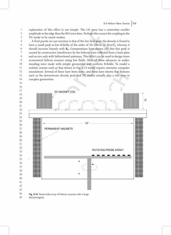
Fig. 6.16 Seven-tube array of helicon sources with a large
electromagnet.
6.4 Helicon Wave Sources 113
1
2
3
4
5
6
7
8
9
10
11
12
13
14
15
16
17
18
19
20
21
22
23
24
25
26
27
28
29
30
31
32
33
34
35
36
37
38
39
40
41
42
43
44
45
6.4.3
Extended Helicon Sources
As in the case of ICPs, helicon sources can also be extended to cover large areas. This
can be done with serpentine antennas [27] or with multiple small tubes. Figure 6.16
shows a distributed source arrayed with one tube surrounded by six others [28]. Each
tube is very short, with a simple m¼ 0 antenna; and a single large magnet coil
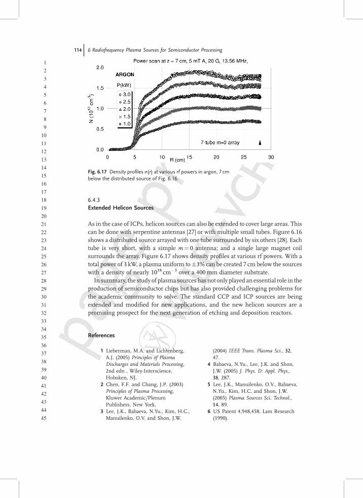
surrounds the array. Figure 6.17 shows density profiles at various rf powers. With a
total power of 3 kW, a plasma uniform to�3% can be created 7 cm below the sources
with a density of nearly 1018 cm�3 over a 400mm diameter substrate.
In summary, the study of plasma sources hasnot only played an essential role in the
production of semiconductor chips but has also provided challenging problems for
the academic community to solve. The standard CCP and ICP sources are being
extended and modified for new applications, and the new helicon sources are a
promising prospect for the next generation of etching and deposition reactors.
References
Fig. 6.17 Density profiles n(r) at various rf powers in argon, 7 cm
below the distributed source of Fig. 6.16.
1 Lieberman, M.A. and Lichtenberg,
A.J. (2005) Principles of PlasmaDischarges and Materials Processing,2nd edn , Wiley-Interscience,
Hoboken, NJ.
2 Chen, F.F. and Chang, J.P. (2003)
Principles of Plasma Processing,Kluwer Academic/Plenum
Publishers, New York.
3 Lee, J.K., Babaeva, N.Yu., Kim, H.C.,
Manuilenko, O.V. and Shon, J.W.
(2004) IEEE Trans. Plasma Sci., 32,47.
4 Babaeva, N.Yu., Lee, J.K. and Shon,
J.W. (2005) J. Phys. D: Appl. Phys.,38, 287.
5 Lee, J.K., Manuilenko, O.V., Babaeva,
N.Yu., Kim, H.C. and Shon, J.W.
(2005) Plasma Sources Sci. Technol.,14, 89.
6 US Patent 4,948,458, Lam Research
(1990).
114 6 Radiofrequency Plasma Sources for Semiconductor Processing

1
2
3
4
5
6
7
8
9
10
11
12
13
14
15
16
17
18
19
20
21
22
23
24
25
26
27
28
29
30
31
32
33
34
35
36
37
38
39
40
41
42
43
44
45
7 US Patent 4,948,458, Applied
Materials (1993).
8 Evans, J.D. and Chen, F.F. (2001)
Phys. Rev. Lett., 86, 5502.9 Kolobov, V.I. and Economou, D.J.
(1997) Plasma Sources Sci. Technol., 6,R1. For example.
10 Meziani, T., Colpo, P. and Rossi, F.
(2001) Plasma Sources Sci. Technol.,10, 276.
11 Colpo, P., Meziani, T. and Rossi, F.
(2005) J. Vac. Sci. Technol. A, 23, 270.12 Lee, Y.J., Han, H.R. and Yeom, G.Y.
(2000) Surf. Coat. Technol., 133, 612.13 Lee, Y.J., Kim, K.N., Song, B.K. and
Yeom, G.Y. (2002) Mater. Sci.Semicond. Process., 5, 419.
14 Lee, Y.J., Kim, K.N., Song, B.K. and
Yeom, G.Y. (2003) Thin Solid Films,435, 275.
15 Kim, K.N., Lee, Y.J., Kyong, S.J. and
Yeom, G.Y. (2004) Surf. Coat.Technol., 177, 752.
16 Park, S.E., Cho, B.U., Lee, J.K., Lee,
Y.J. and Yeom, G.Y. (2003) IEEETrans. Plasma Sci., 31, 628.
17 Boswell, R.W. (1970) Phys. Lett. A,33, 457.
18 Boswell, R.W. (1984) Plasma Phys.Control. Fusion, 26, 1147.
19 Tynan, G.R., Bailey, A.D., III,
Campbell, G.A., Charatan, R.,
deChambrierA., Gibson, G., Hemker,
D.J., Jones, K., Kuthi, A., Lee, C.,
Shoji, T. and Wilcoxson, M. (1997) J.Vac. Sci. Technol. A, 15, 2885.
20 Miljak, D.G. and Chen, F.F.
(1998) Plasma Sources Sci. Technol., 7,61.
21 Chen, F.F. (1991) Plasma Phys.Control. Fusion, 33, 339.
22 Blackwell, D.D. and Chen, F.F.
(2001) Plasma Sources Sci. Technol.,10, 226.
23 Shamrai, K.P. and Sharanov, V.B.
(1995) Plasma Phys. Control. Fusion,36, 1015. (1996) Plasma Sources Sci.Technol, 5, 43.
24 Arnush, D. (2000) Phys. Plasmas, 7,3042.
25 Blackwell, D.D., Madziwa, T.G.,
Arnush, D. and Chen, F.F. (2002)
Phys. Rev. Lett., 88, 145002.26 Chen, F.F. (2003) Phys. Plasmas, 10,
2586.
27 Jewett, R.F.Jr., (1995) PhD thesis,
University of New Mexico.
28 Chen, F.F., Evans, J.D. and Tynan,
G.R. (2001) Plasma Sources Sci.Technol., 10, 236.
References 115

1
2
3
4
5
6
7
8
9
10
11
12
13
14
15
16
17
18
19
20
21
22
23
24
25
26
27
28
29
30
31
32
33
34
35
36
37
38
39
40
41
42
43
44
45