structure and morphology of diamond-like carbon … and morphology of diamond-like carbon coated on...
TRANSCRIPT

Structure and Morphology of Diamond-like Carbon Coated
on Nylon 66/Poly(phenylene ether) Alloy
Akira IGARASHI2, Hiroshi HAYASHI3, Takeshi YAMANOBE1, Tadashi KOMOTO1,+
1Department of Chemistry, Gunma University, Kiryu, Gunma 376-8515, Japan 2Tomo Research Center of Gunma Prefecture, 1058-5 Yoshizawa-cho, Ota, Gunma
373-0019, Japapn 3Kurita Seisakusho Co. Ltd., 2112 Soja, Soja-machi, Maebashi. Gunma 371-0852, Japan
Abstract
In order to investigate the structure and morphology of diamond-like carbon (DLC)
film coated on a polymer alloy prepared by a particular four-steps method in the
plasma-based ion implantation and deposition (PBIID) process, studies were made on
the structure and properties of the DLC film with special reference to its surface
morphology by scanning (SEM) and transmission (TEM) electron microscopies. It is
revealed from TEM microscopy that the amorphous structure of the DLC film consists
of a silicon-implanted layer on the polymer substrate, a hard acetylene-implanted layer
and a flexible acetylene/toluene-deposited layer. Some properties of the DLC film can
be accounted for by the morphology examined in this study.
KEY WORDS diamond-like carbon / DLC / coating / plasma / implantation / polymer
alloy / TEM / XPS
1

______________________________________________________________________
________________
+ To whom correspondence should be addressed (Tel: +81-277-30-1330. E-mail:
2

Surface treatments of polymeric materials1 are important methods for various
industrial, medical and other applications. Plasma chemistry plays a role in surface
treatment of polymers through use of low temperature glow discharge, ion beam
bombardment and so on in gaseous state.2,3
Since Aisenberg et al.4 applied ion beam to deposition of thin diamond-like carbon
(DLC) film, a sort of network polymers mainly consisting of carbon and hydrogen, onto
other materials, attentions have been paid to its hardness similar to diamond,
tribological properties with low friction and wear, gas barrier properties, improved
blood compatibility and so on.5 As is reviewed by Suzuki et al.6, many studies were
made on the structures and properties, methods for preparation and applications of
various kinds of coated DLC films.
Of these properties of DLC films, their tribological properties are of great interest
because of their roles in improving the surface properties of metals, ceramics, polymers
and composites by DLC coatings with special reference to their chemical structures,
variable hardness, and low friction and wear.
Recently, studies on DLC coatings onto polymer surfaces have been increasingly
focused on their friction and wear properties,7-17 a few on gas barrier enhancement14,15,18
and so on. In these studies, the tribological properties of DLC-coated polymers are
mainly discussed in relation to the surface hardness and roughness, adhesive strength
and surface morphology measured by optical and scanning electron microscopies.
However, no detailed morphological study has been so far reported on the DLC films
coated onto polymer surfaces by means of transmission electron microscopy (TEM)
which may be a promising method for revealing the interface structure.
Of various DLC coating methods developed so far, ion beam deposition and ion
beam assisted deposition methods are not preferred to complicated geometry of
substrate specimens, and plasma-enhanced chemical vapor deposition and pulsed laser
deposition methods usually need heating of specimens.19 On the other hand, a very
recently developed method, i.e., a hybrid process of plasma-based ion implantation and
deposition (PIIBD)20 is promising for polymeric substrates because of prevention of
temperature increase and residual compressive stress almost two orders less than that for
3

conventional methods for DLC films on quartz glass plate.21 In addition, PBIID can
produce a mixing interface between a DLC film and a substrate and a uniform DLC film
coating on three dimensional substrate. 21,22 In this study, PIIBD method is applied to
DLC coating onto a polymer alloy.
In this paper, we will mainly report on the structure and morphology of a
DLC-coated polymer alloy, consisting of nylon 66 and poly(phenylene ether), prepared
by the PBIID method and its properties will be also discussed. The present study will
be of importancet for investigation of the tribological properties of DLC-coated
polymers by the PBIID method.
EXPERIMENTAL
Polymeric substrates
As for a polymeric substrate for DLC coating, Noryl GTX6601 of GE Plastics Co.
was chosen, which is a polymer alloy consisting of nylon 66 matrix and modified
poly(phenylene ether) (PPE) domains, having properties such as dimensional stability,
low water absorption, heat resistance and chemical resistance..
The polymer specimen subjected to DLC coatings was injection-molded into disks
with a diameter of 70 mm and a thickness of 5 mm.
DLC film coating
The DLC film coating onto the polymeric surface was carried out according to the
PBIID method.20,22 A schematic diagram of PBIID system is shown in Fig. 1. In this
system, RF pulse for plasma generation was supplied to the substrate together with a
negative high voltage pulse for ion implantation through a single electrical feed-through
using a matching circuit for both pulses. As the substrate itself was used as an RF
antenna, uniform plasma was generated around the substrate. A four-steps procedure for
DLC coating20 was carried out in this experiment. The sequence for DLC film coating
procedure is summarized in Table 1.
Prior to DLC film coating, the disk specimen surface was sputter-cleaned for 10 min
in the first step using a 300 W RF plasma of mixed gas of Ar (50%) and CH4 (50%) at a
4

pressure of 0.4 Pa with a negative medium-voltage pulse (voltage: -5 kV, duration: 5
�s, repetition rate: 2 kHz) in a stainless steel reaction chamber, 20 which has a gas inlet
with a pressure and flow control system and a connection to pump through an oil
diffusion pump. Flow rate of each gas was 30 cm3/min.
In order to produce a mixing interface between the polymeric substrate and DLC
film to be coated for their improved adhesion, silicon ion implantation with a high
voltage pulse (voltage: -5 kV, duration: 5 �s, repetition rate: 1 kHz) and RF output
power of 300 W was performed through the single electrical feed-though in the second
step, where were made a flow rate of 15 cm3/min and a flow time of 15 min of a
precursor gas hexamethyl disiloxane (HMDS) for silicon implantation.
The third step was carried out to further produce the second mixing interface and
then to produce DLC film using acetylene (C2H2) plasma by the same method as
applied to the silicon ion implantation except for a flow rate of 100 cm3/min and a flow
time of 30 min.
In the last fourth step, deposition of DLC film was made using a mixed gas of C2H2
(flow rate: 90 cm3/min) and toluene (C6H5CH3, flow rate: 20 cm3/min) with a flow time
of 240 min.
X-Ray photoelectron spectroscopy (XPS)
Chemical elements of the specimen surface were measured by XPS under a pressure
of 1.33 x 10⁻⁶ Pa in an Axis-HS spectrometer of Kratos Analytical, Ltd., using
monochromated X-ray emitted from Al anode at a power of 150 W. The pass energy for
measuring survey and element spectra was 160 eV and 40 eV, respectively. A charge
neutralizer was equipped with the spectrometer to prevent peak shifts in the XPS
spectrum due to specimen charging induced by X-ray irradiation. An XPS spectrum was
recorded for specimen obtained in each PBIID step.
Raman scattering spectroscopy
In order to analyze the structure of the resultant coated DLC film, Raman scattering
spectroscopy was carried out using an Ar laser with a wavelength of 514.5 nm in a
5

Renishaw Ramanoscope spectrometer, recording spectra over a Raman shift range from
200 to 3600 cm-1.
Coated DLC film thickness measurement
The resultant coated DLC film thickness was measured in a Mitsutoyo SV-9634
surface roughness measuring system. After the PBIID procedure was made onto the
polymer specimen surface with a piece of an adhesive tape thereon, the tape was peeled
off to obtain a part of the specimen surface without DLC film and then the step height
was measured at the coated DLC film edge thus formed in the boundary of surfaces
with and without DLC film.
Nanoindentaion measurement
Surface hardness of the neat polymer alloy and the DLC film coated thereon was
measured by nanoindentation in a JEOL JSPM-4210 Scanning Probe Microscope
equipped with a Berkovich-type of diamond indenter (tip). According to a reported
method,23 experiments were made using a triangular load-time profile, such that the
nanoindenter was first loaded to a peak load (300 �N or 500 �N) in 5 min and then
unloaded in 5 min, recording load-displacement curves during a loading and unloading
cycle. Hardness, defined as the pressure under the tip given by the ratio of force to the
projected area of plastic deformation, was estimated from the load-displacement curve.
The measurement was carried out at 10 different positions of each specimen surface.
Adhesive strength measurement
Adhesive strength of coated DLC film and polymeric substrate was measured as a
tensile strength to break using a Rheotech Rheometer RT-2020J-CW. The DLC-coated
surface was first plasma etched to enhance an adhesion with a glue. A 5 mm x 5mm
square part of the DLC-coated specimen surface was cut by a stainless knife, deep into
the polymer substrate just beneath the interface layer. A nylon fiber was then adhered
onto the square part using an instantaneously polymerizable cyanoacrylate resin as a
glue. After complete adhesion, the specimen thus obtained was subjected to tensile
6

measurement in the rheometer by drawing normal to the specimen surface at a drawing
speed of 6 cm/min.
Scanning electron microscopy (SEM)
Surface morphology of the DLC-coated polymer alloy prepared in each step was
examined by a JEOL JSM-6700F field-emission scanning electron microscope after the
specimen was coated by Pt with a thickness of 5 nm using a JEOL Auto-Fine Coater
JFC-1600.
Transmission electron microscopy (TEM)
Embedding of the DLC-coated samples in an epoxy resin was chosen for
preparation of TEM specimen. The sample, which had been cut into a small block
suitable for further preparation, was subjected to a treatment by low temperature air
plasma generated at 13.56 MHz under a pressure of ca. 13.3 Pa in a Samco Plasma
Deposition System Model BP-1 to make the sample surface hydrophilic for a better
adhesion to epoxy resin to be embedded therein. The plasma-treated specimen was
embedded in an Oken epoxy resin consisting of 2.6 g Epok 812, 1.5 g DDSA, 1.2 g
MNA and a few drops of DMP-30, and then cured overnight at 60oC. OsO4-staining was
made at 60 oC for 3 h in the vapor phase of solid OsO4 in order to make the polymeric
substrate hard for easy ultrathin sectioning at room temperature . Ultrathin sectioning
was made using a diamond knife in a Reichert-Jung Ultracut microtome. The ultrathin
sections with thickness of 50 - 60 nm of the OsO4-stained specimens were collected on
copper grids. TEM observation was made at an accelerating voltage of 80 kV in a JEOL
1200EX transmission electron microscope equipped with a LaBB6 filament.
RESULTS AND DISCUSSION
Changes in surface structure in the PBIID process
In order to investigate the changes of surface structure of the polymer alloy Noryl
GTX6601 consisting of nylon 66 and PPE in the PBIID process, XPS experiment was
7

made on the surface of specimen obtained in each PBIID step. Fig. 2 shows XPS spectra
of surfaces of neat polymer alloy (a), Ar sputter-etched polymer alloy (b) obtained in the
first step, Ar sputter-etched and then silicon ion-implanted polymer alloy (c) obtained in
the second step, Ar sputter-etched, silicon ion-implanted and then C2H2-implanted
polymer alloy (d) obtained in the third step, and Ar sputter-etched, silicon ion-implanted,
C2H2-implanted and then C2H2/C6H5CH3-deposited polymer alloy (e) obtained in the
fourth step.
From the chemical structures of nylon 66 (-NH(CH2)6NHCO(CH2)4CO-) and PPE
(-C6H4(CH3)2-O-), an elemental ratio C:N:O is estimated as 6:1:1 and 8:0:1, respectively.
The alloy contains nearly equal amounts of nylon 66 and PPE according to our NMR
study.24 Thus, this polymer alloy should contain a large amount of carbon, the least
amount of nitrogen and a small amount of oxygen. An XPS spectrum shown in Fig. 2
(a) indicates that the intensity is stronger for oxygen than for carbon. In addition, weak
peaks for Si 2s and Si 2p are measured in the spectrum, though the polymer alloy
contains no silicon compounds. This result indicates that the strong O1s peak and Si2s
and Si2p peaks are due to contaminants such as silica deposited on the specimen. A very
weak peak appearing at 400 eV can be assigned to N1s of nylon 66.
As shown in Fig. 2 (b), a strong C1s peak, medium strong O1s peak and no Si2s and
Si2p peaks indicate that the polymer alloy surface was completely cleaned by Ar
sputtering in the first step of the PBIID process. Fig. 2 (c) shows that silicon was
implanted into the cleaned polymer alloy surface as is evident from medium strong Si2s
and Si2p peaks. The intensity of O1s peak stronger than that of C1s one may be due to
implanted oxygen together with silicon because HMDS was used as a precursor. This
result suggests that oxygen tends to be implanted more than carbon, although HMDS
contains 6 carbon atoms and 1 oxygen atom in the molecule. It is also noted that the
intensity of N1s peak decreased down to a noise level, indicating that silicon was
homogeneously implanted over the whole range of the polymer alloy surface.
Fig. 2 (d) shows an XPS spectrum of the C2H2-implanted surface obtained in the
third step. This spectrum clearly indicates a drastic change in the surface structure such
that Si2s and Si2p peaks completely disappeared and the O1s intensity is weak as
8

compared with that of C1s. In addition, N1s peak also disappeared. This result suggests
that C2H2-implantation was successfully made onto the silicon-implanted polymer alloy
surface.
An XPS spectrum shown in Fig. 2 (e), which was measured for the
C2H2/C6H5CH3-deposited polymer alloy obtained in the last step, is very similar to that
of Fig, 2 (d), except for a little increase in O1s intensity probably due to somewhat an
effect of the ambient air because a noise level N1s peak also appears in the spectrum.
Taking into consideration that the XPS measurement was done for the specimen once
exposed to air for a certain time after the PBIID process, the appearance of oxygen peak
does not always indicate oxygen implantation in the PBIID process. The content of
oxygen is estimated to be much lower in the coated DLC film than that measured by the
XPS experiment, though the existence of oxygen in the coated DLC film can not be
denied.
Structure of coated DLC film
As is reviewed in literatures,6,15,25,26 the structure of DLC is amorphous, consisting
of both sp3 and sp2 bondings, while diamond and graphite, which are both crystalline,
are composed of sp3 and sp2 bondings, respectively. Namely, DLC has both diamond
structure with sp3 bondings and graphite structure with sp2 bondings. Additional sp3
C-H bondings give rise to a long-range disordered structure of DLC.26 Raman scattering
spectroscopy is useful for characterizing DLC structure such that broad Raman bands
centered at ca.1350 cm-1 (D-band) and 1580 cm-1 (G-band) are assigned to the
disordered and graphite structure, respectively.6,25 In Fig. 3 is shown a Raman spectrum
of the DLC film coated onto the polymer alloy obtained in the fourth step of the PBIID
process. The spectrum has two distinctive peaks at ca. 1360 cm-1 and ca. 1580 cm-1,
typical of DLC film. This result clearly indicates that the DLC film was coated on the
silicon- and C2H2-implanted interface which had been formed on the polymer alloy
surface, as is evident from the XPS results mentioned above.
9

Thickness of coated DLC film
Thickness of the DLC film coated on the polymer alloy was estimated as ca.1 �m
by measuring its step height as was mentioned in experimental. Taking into
consideration that the third and fourth steps for 30 min and 240 min, respectively at
similar gas flow rates, in the DLC coating process contribute to the resultant film
thickness, an average rate of DLC film thickening can be estimated as ca. 3.7 nm/min.
Adhesive strength
Adhesive strength as an average tensile strength to break for the DLC-coated
polymer alloy was estimated as 2.4 MPa. It is noted that the tensile break of the
specimen took place at the glue resin. The true adhesive strength of the DLC-coated
polymer alloy may be, therefore, higher than 2.4 MPa.
The above-obtained adhesive strength with magnitude of a few MPa is comparable
to reported values of 1.1 – 3.0 and 2.0 – 3.7 MPa for DLC-coated polyethylene and
silicone, respectively.8
Surface hardness of coated DLC film
It is of interest to estimate a difference in surface hardness of the polymer alloy and
the coated DLC film. A measured hardness depends on the size of indenter because of
easy deformation of polymer surface with a very thin DLC film coated thereon. Thus,
the hardness was measured by nanoindentation. The measured surface hardness was
0.10 – 0.14 GPa and 2.14 – 3.54 GPa for the polymer alloy with and without
DLC-coating, respectively. Fig. 4 shows a large difference in hardness between the
polymer alloy surface (average hardness: ca. 0.12 GPa) and the coated DLC film
(average hardness: ca. 2.96 GPa), indicating a hardness of the DLC film ca. 25 times
that of the polymer surface. The large difference in hardness between the specimens
suggests almost no deformation of the polymer substrate during measuring hardness of
the DLC film.
10

Surface morphology of coated DLC film
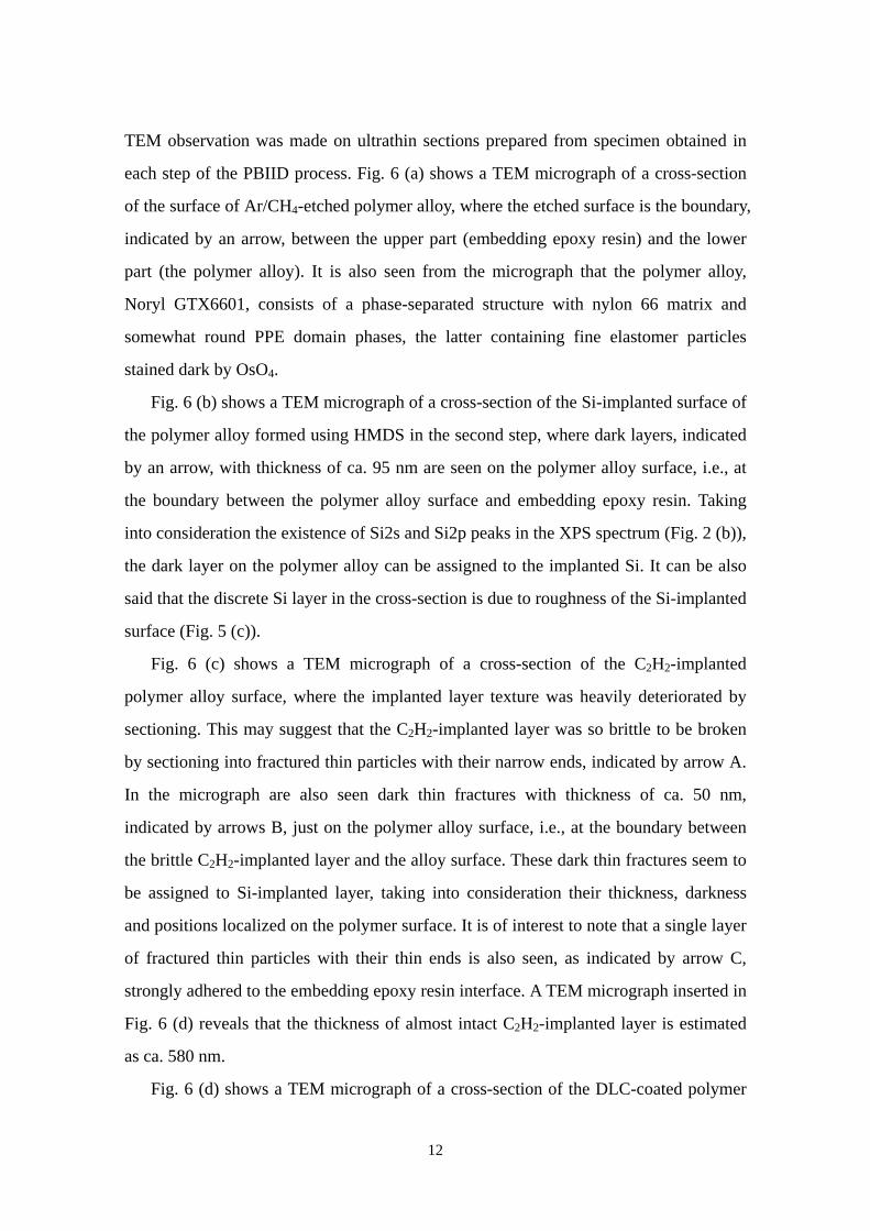
Fig. 5 shows SEM micrographs of the polymer alloy surface obtained in each step of
the PBIID process. Fig. 5 (a) shows a surface morphology of the neat polymer with
as-mold surface roughness. The surface turned rather smooth after Ar sputter-etching
(Fig. 5 (b)). Fig. 5 (c) shows the Ar sputter-etched and then silicon ion-implanted
polymer surface, whose morphology seems to be similar to that shown in Fig. 5 (b)
except for formation of ca. 0.2 �m-thick particles and a little ill-shaped rough edges on
the surface.
A drastic change in surface morphology was found in Fig. 5 (d) by the
C2H2-implantation, where both smooth part and rough edges shown in Fig. 5 (c) were
covered with nearly round particles with sizes less than ca. 2 �m. Coagulated particles
with sizes of a few micrometers are also seen. It is of interest that the former smooth
part still remained, while the latter rough edges were covered with large particles. This
may indicate a heterogeneity in rate of implantation or deposition of DLC such that the
rate is higher at rough edges than at smooth part of the surface.
Fig. 5 (e) shows a TEM micrograph of the surface after the
C2H2/C6H5CH3-deposition, which is similar to the morphology shown in Fig. 5 (d). It is
likely, however, that the morphology is somewhat smoother for the
C2H2/C6H5CH3-deposited surface than for the C2H2-deposited one. In addition, the
fraction of large coagulated particles decreased and the size of most particles is less than
ca. 1 �m. It may be said that the deposition of DLC onto rough edges of the surface
was suppressed in case of C2H2/C6H5CH3-deposition.
The surface roughness of the resultant DLC film deposited in the last fourth step is
anyhow not smooth as is evident from Fig. 5 (e), indicating a heterogeneity in DLC film
thickness. The various surface hardnesses of 2.14 – 3.54 GPa may be accounted for by
the heterogeneity of DLC film thickness, which is partly due to the original surface
roughness of the polymer specimen itself.
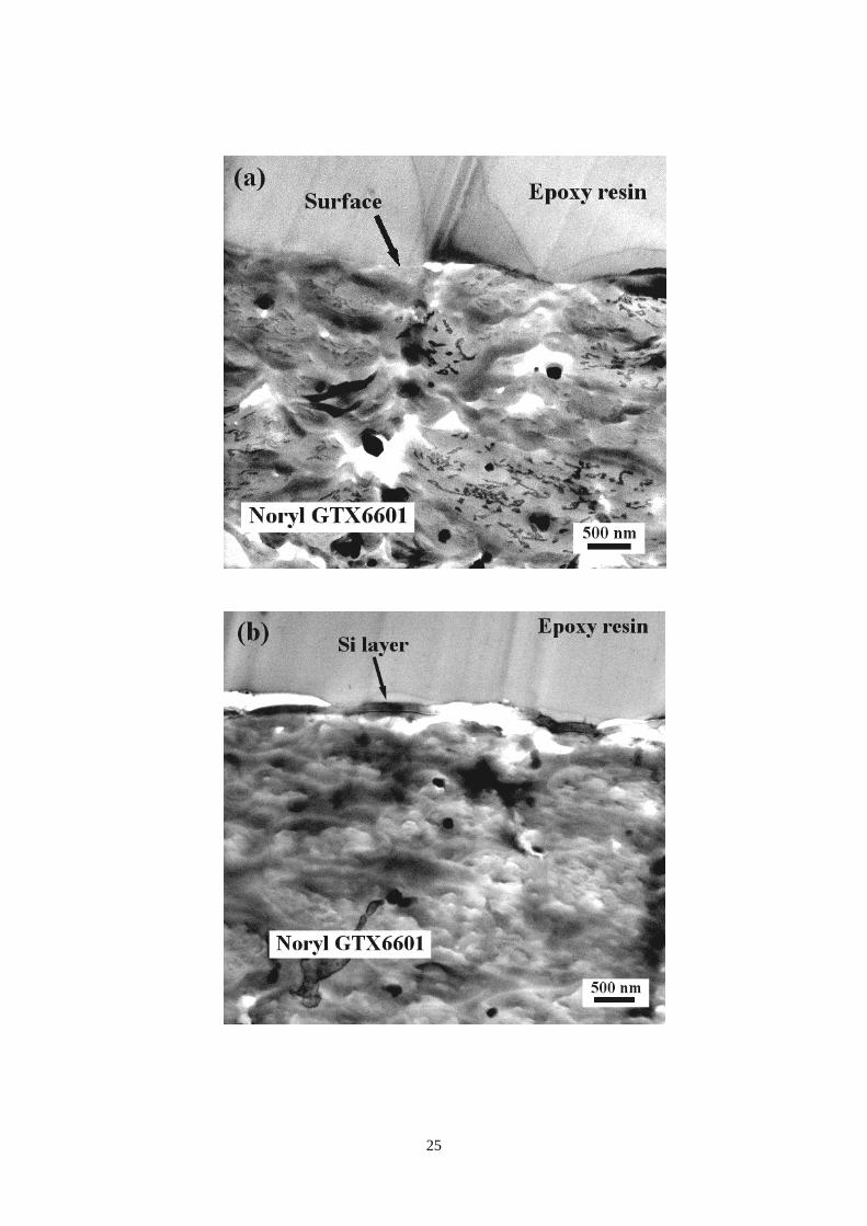
Morphology of the interface
In order to examine the detailed morphology of the DLC-coated polymer alloy,
11
TEM observation was made on ultrathin sections prepared from specimen obtained in
each step of the PBIID process. Fig. 6 (a) shows a TEM micrograph of a cross-section
of the surface of Ar/CH4-etched polymer alloy, where the etched surface is the boundary,
indicated by an arrow, between the upper part (embedding epoxy resin) and the lower
part (the polymer alloy). It is also seen from the micrograph that the polymer alloy,
Noryl GTX6601, consists of a phase-separated structure with nylon 66 matrix and
somewhat round PPE domain phases, the latter containing fine elastomer particles
stained dark by OsO4.
Fig. 6 (b) shows a TEM micrograph of a cross-section of the Si-implanted surface of
the polymer alloy formed using HMDS in the second step, where dark layers, indicated
by an arrow, with thickness of ca. 95 nm are seen on the polymer alloy surface, i.e., at
the boundary between the polymer alloy surface and embedding epoxy resin. Taking
into consideration the existence of Si2s and Si2p peaks in the XPS spectrum (Fig. 2 (b)),
the dark layer on the polymer alloy can be assigned to the implanted Si. It can be also
said that the discrete Si layer in the cross-section is due to roughness of the Si-implanted
surface (Fig. 5 (c)).
Fig. 6 (c) shows a TEM micrograph of a cross-section of the C2H2-implanted
polymer alloy surface, where the implanted layer texture was heavily deteriorated by
sectioning. This may suggest that the C2H2-implanted layer was so brittle to be broken
by sectioning into fractured thin particles with their narrow ends, indicated by arrow A.
In the micrograph are also seen dark thin fractures with thickness of ca. 50 nm,
indicated by arrows B, just on the polymer alloy surface, i.e., at the boundary between
the brittle C2H2-implanted layer and the alloy surface. These dark thin fractures seem to
be assigned to Si-implanted layer, taking into consideration their thickness, darkness
and positions localized on the polymer surface. It is of interest to note that a single layer
of fractured thin particles with their thin ends is also seen, as indicated by arrow C,
strongly adhered to the embedding epoxy resin interface. A TEM micrograph inserted in
Fig. 6 (d) reveals that the thickness of almost intact C2H2-implanted layer is estimated
as ca. 580 nm.
Fig. 6 (d) shows a TEM micrograph of a cross-section of the DLC-coated polymer
12
alloy obtained in the last step of the PBIID process. Compared with the morphology
shown in Fig. 6 (c), a very dark layered texture, indicated by an arrow A, with thickness
of ca. 320 nm is seen in the interface between the polymer alloy and the embedding
epoxy resin. Therefore, this dark layered texture highly stained by OsO4 should be
formed in the C2H2/C6H5CH3-deposition step.
The interface in the cross-section at A consists of three layers: the Si-implated layer
(shown by arrow B), the intermediate C2H2-implanted layer (arrow C) and the
C2H2/C6H5CH3-deposited layer (arrow A), with thickness of ca. 50 nm, ca. 240 nm and
320 nm, respectively. Another part of the cross-section at D consists of apparent two
layers: ca. 400 nm-thick C2H2-implanted layer and ca. 250 nm-thick
C2H2/C6H5CH3-deposited layer, the Si-implanted layer being likely obscure.
The total thickness of the DLC film coated on the polymer alloy is estimated as ca.
660 nm and 650 nm at position A and D, respectively, which are somewhat less than the
value of ca. 1 �m estimated by a surface roughness measuring system.
Closer looking at these TEM micrographs of the OsO4-stained ultrathin
cross-sections, it is of great interest that the C2H2/C6H5CH3-deposited layer is darkest of
all, Si-implanted one intermediately dark and the C2H2-implanted one is rather bright.
Taking into consideration the chemical composition of carbon and hydrogen in these
layers except for Si-implanted one, darkness depends on the reactivity with OsO4. It is
thought that the lower the density (or the higher the mobility) of materials is, the higher
the reactivity of OsO4. That is to say, low density materials are so stained by OsO4 to be
seen dark in TEM observation. As this DLC is amorphous, the density of the
C2H2/C6H5CH3-deposited layer can be estimated to be lower than that of the
C2H2-implanted one and the molecular mobility of the DLC prepared by
C2H2/C6H5CH3-deposition is high.
It can be, therefore, concluded that the present DLC-film coated on the polymer
alloy consists of a C2H2/C6H5CH3-deposited layer with a high flexibility and hard Si-
and C2H2-implanted intermediate layers. This result is also consistent with the formation
of a smooth surface by C2H2/C6H5CH3-deposition (Fig. 5 (d)). It is worthy of note that a
low structural strain21 of the PBIID-processed DLC film was first verified in this
13

morphological study.
It is also of interest to investigate tribology of the DLC-coated polymer alloy with a
moderate hardness and flexibility because this sort of DLC film with particular structure
and properties is said to give a low friction and wear under mild friction conditions. A
tribological study of this polymer alloy will be reported elsewhere.
14
References
1) “Hyomen Shori Handbook,” H. Mizumachi, M. Tobayama, Ed., NTS publisher,
Tokyo, 2000.
2) “Techniques and Applications of Plasma Chemistry,” J. R. Hollahan, A. T. Bell, Ed.,
Wiley Interscience, New York, 1974.
3) T. Komoto, in “Processing of Polymers by the Energy Beam,” S. Tazuke, Y. Osada,
I. Kaetsu, Ed., CMC publisher, Tokyo, 1986, p.163.
4) S. Aisenberg, R. Chabot, J. Appl. Phys., 42, 2953 (1971).
5) R. Hauert, U. Meuller, Diamond Relat. Mater., 12, 171 (2003).
6) H. Suzuki, M. Ikenaga, “DLC Seimaku Gijuttsu,” H. Suzuki, M. Ikenaga, Ed.,
Nikkan Kogyo Shinbunsha, Tokyo, 2003.
7) S. J. Bull, A. R. McCabe, A. M. Jones, Surf. Coat. Technol., 64, 87 (1994).
8) K. Donnelly, D. P. Dowling, M. L. McConnell, R. V. Flood, Diamond Relat. Mater.,
8, 538 (1999).
9) J. Hyun, M. Pope, J. Smith, M. park, J. J. Cuomo, J. Appl. Polymer Sci., 75, 1158
(2000).
10) X. T. Zhou, S. T. Lee, I. Bello, A. C. Cheung, D. S. Chiu, Y. W. Lam, C. S. Lee, K.
M. Leung, X. M. He, Surf. Coat. Technol., 123, 273 (2000).
11) S. Miyake, T. Saitoh, S. Watanabe, E. Hayashi, T. Nakamaru, Hyomen Gijutsu, 52,
878 (2001).
12) T. Nakahigashi, K. Miyake, Y. Murakami, Tribologist, 47, 833 (2002).
13) Y.-B. Guo, F. C.-N. Hong, Diamond Relat. Mater., 12, 946 (2003).
14) K. Inagawa, T. Zeniya, N. Hibino, Surf. Coat. Technol., 169-170, 344 (2003).
15) T. Nakahigashi, Y. Tanaka, K. Miyake, H. Oohara, Tribol. Inter., 37, 907 (2004).
16) V. P. Paliakov, C. J. de M. Siqueira, W. Veiga, I. A. Heummelgen, C. M. Lepienski,
G. G. Kirpilenko, S. T. Dechandt, Diamond Relat. Mater., 13, 1511 (2004).
17) D. Sheeja, B. K. Tay, L. N. Nung, Surf. Coat. Technol., 190, 231 (2005).
18) Y. Yamashita, Kobunshi, 52, 902 (2003).
19) J. X. Liao, W. M. Liu, T. Xu, Q. J. Xue, Appl. Surf. Sci., 226, 387 (2004).
15

20) Y. Nishimura, A. Chayahara, Y. Horino, M. Yatsuzuka, Surf. Coat. Technol., 156, 50
(2002).
21) Y. Oka, M. Kirinuki, Y. Nishimura, K. Azuma, E. Fujiwara, M. Yatsuzuka, Surf.
Coat. Technol., 186, 141 (2004).
22) Y. Oka, Y. Nishimura, M. Yatsuzuka, Vacuum, 73, 541 (2004).
23) Y. Xiaohan, R. C. Hsaio, D. B. Bogy, IEEE Trans. Magn., 33 (1. Pt.2, 7th Annual
Magnetic Recording Conference on Media), 938 (1997).
24) T. Yamanobe, M. Terao, A. Igarashi, T. Komoto, unpublisheid data.
25) H. –J. Scheibe, D. Drescher, P. Alers, Fressenius’ J. Anal. Chem., 353, 695 (1995).
26) J. Robertson, Mater. Sci. Eng. R. Rep., 37, 129 (2002).
16

Figure 1 Schematic illustration of DLC-coating equipment for PBIID process.
17

18

19

Figure 2. XPS spectra of as-mold polymer surface (a), Ar/CH4-cleaned surface (b),
HMSD-implanted surface (c), C2H2-implanted surface (d) and C2H2/C6H5CH3-deposited surface (e).
20

Figure 3. Raman scattering spectrum of DLC film coated onto the polymer.
Figure 4. Surface hardness of the as-mold polymer and DLC film coated thereon.
21

22
23

Figure.5. SEM micrographs of as-mold polymer surface (a), Ar/CH4-cleaned surface
(b), HMSD-implanted surface (c), C2H2-implanted surface (d) and C2H2/C6H5CH3-deposited surface (e).
24
25

Figure 6. TEM micrographs of OsO4-stained ultrathin cross-section of polymer surface subjected to Ar/CH4-cleaned surface (a), HMSD-implantation (b), C2H2-implantation (c) and
C2H2/C6H5CH3-deposition (d).
26

Table 1 DLC deposition parameters
Process Gas Flow rate (cc/min) Time (min)
1: Cleaning Ar + CH4 30 + 30 10
2: Ion implantation HMDS 15 15
3: DLC deposition C2H2 100 30
4: DLC deposition C2H2 + Toluene 90 + 20 240
27