study of high precision igbt macro-model considering
TRANSCRIPT

Study of High Precision IGBT Macro-Model Considering Temperature Dependency
Masaki Kazumi*, Hitoshi Aoki, Yukiko Arai, Ramin Khatami, Shunichiro Todoroki, Takuya Totsuka, Fumitaka Abe, Haruo Kobayashi
Division of Electronics and Informatics, Gunma University 1-5-1 Tenjin-cho Kiryu 376-8515 Japan [email protected] [email protected]
Abstract—In this study, a novel SPICE model of an Insulated-Gate-Bipolar-Transistor of (IGBT), which is often used to handle high power signals in automotive electrical circuits, has been developed. The model consists of basic SPICE elements. Thus, it can be used in any SPICE-compatible simulators without any source code modifications. This paper reports the results of drain current characteristics considering the temperature dependence by using the proposed IGBT macro-model for SPICE.
Keywords— Insulated Gate Bipolar Transistor, IGBT, SPICE, Macro Model )
I. INTRODUCTION Insulated Gate Bipolar Transistor (IGBT) is suitable for high-voltage and large current applications. Because IGBT is voltage-controlled device with the insulated gate, it is mainly applied for high voltage semiconductor elements for car electronic systems. IGBT models for circuit simulations have been implemented in any standard SPICE libraries [1]. However, existing SPICE models are not so accurate to simulate IGBT device behavior comparing with actual measurements. Therefore, model improvements are necessary to apply them for practical circuit design. Our study is to develop the SPICE IGBT macro-model by high voltage semiconductor elements for car electronic systems. An IGBT model for circuit simulations has been developed as a SPICE sub-circuit. The model consists of basic SPICE elements to improve accuracies without any source code modifications. Hence, it can be used in any SPICE-compatible simulators. This paper reports the results of drain current static characteristic considering the temperature dependence by using the proposed IGBT macro-model for SPICE simulators.
II. BASIC PRINCIPLES OF IGBT
A. Typical structure of IGBT IGBT is the structure of power MOSFET (DMOS transistor) by appending the high diffusion rate p-layer. Fig. 1 [2] shows the device structure of IGBT. When enough voltage is applied to the gate under forward bias between anode and cathode terminals condition, an inversion layer is formed in p-layer to the vicinity of the gate electrode. Current flows the n- layer through the inversion layer, and holes are injected toward the n- layer from the p-layer. This hole moves the n- layer which is
basically the drift layer by diffusion, and the part of them are recombined with electrons which passing through the drift layer. Remained halls flow into the p-layer through the junction. In other words, conduction has been made between the anode and the cathode. It can be seen that this is an on-state pnp bipolar transistor, whose p+ layer is the emitter of the hall, p-layer is the collector (cathode), and n-layer is the base (gate).
Fig. 1. Simplified structure of IGBT
B. The static characteristics of the IGBT Fig.2 shows static DC output characteristics of IGBT [2].
Fig. 2. Static DC output characteristics of IGBT [2]
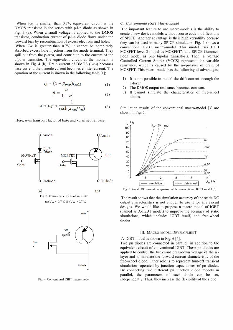
When VAK is smaller than 0.7V, equivalent circuit is the DMOS transistor in the series with p-i-n diode as shown in Fig. 3 (a). When a small voltage is applied to the DMOS transistor, conduction current of p-i-n diode flows under the forward bias by recombination of excess electrons and holes. When VAK is greater than 0.7V, it cannot be completely absorbed excess hole injection from the anode terminal. They spill out from the p-area, and contribute to the current of the bipolar transistor. The equivalent circuit at the moment is shown in Fig. 4 (b). Drain current of DMOS (IMOS) becomes base current, then, anode current becomes emitter current. The equation of the current is shown in the following table [1];
(1)
(2)
(3)
Here, αT is transport factor of base and xnn is neutral base.
Fig. 3. Equivalent circuits of an IGBT
(a) VAK < 0.7 V, (b) VAK > 0.7 V.
Fig. 4. Conventional IGBT macro-model
C. Conventional IGBT Macro-model The important feature to use macro-models is the ability to create a new device models without source code modifications of SPICE. Another advantage is their high versatility because they can be used in many SPICE simulators. Fig. 4 shows a conventional IGBT macro-model. This model uses UCB MOSFET level 3 model as MOSFET’s and SPICE Gummel-Poon model as pnp bipolar transistor’s. Then, a Voltage Controlled Current Source (VCCS) represents the variable resistance, which is caused by the n-epi-layer of drain of MOSFET. This macro-model has the following disadvantages, 1) It is not possible to model the drift current through the
n-layer. 2) The DMOS output resistance becomes constant. 3) It cannot simulate the characteristics of free-wheel
diodes.
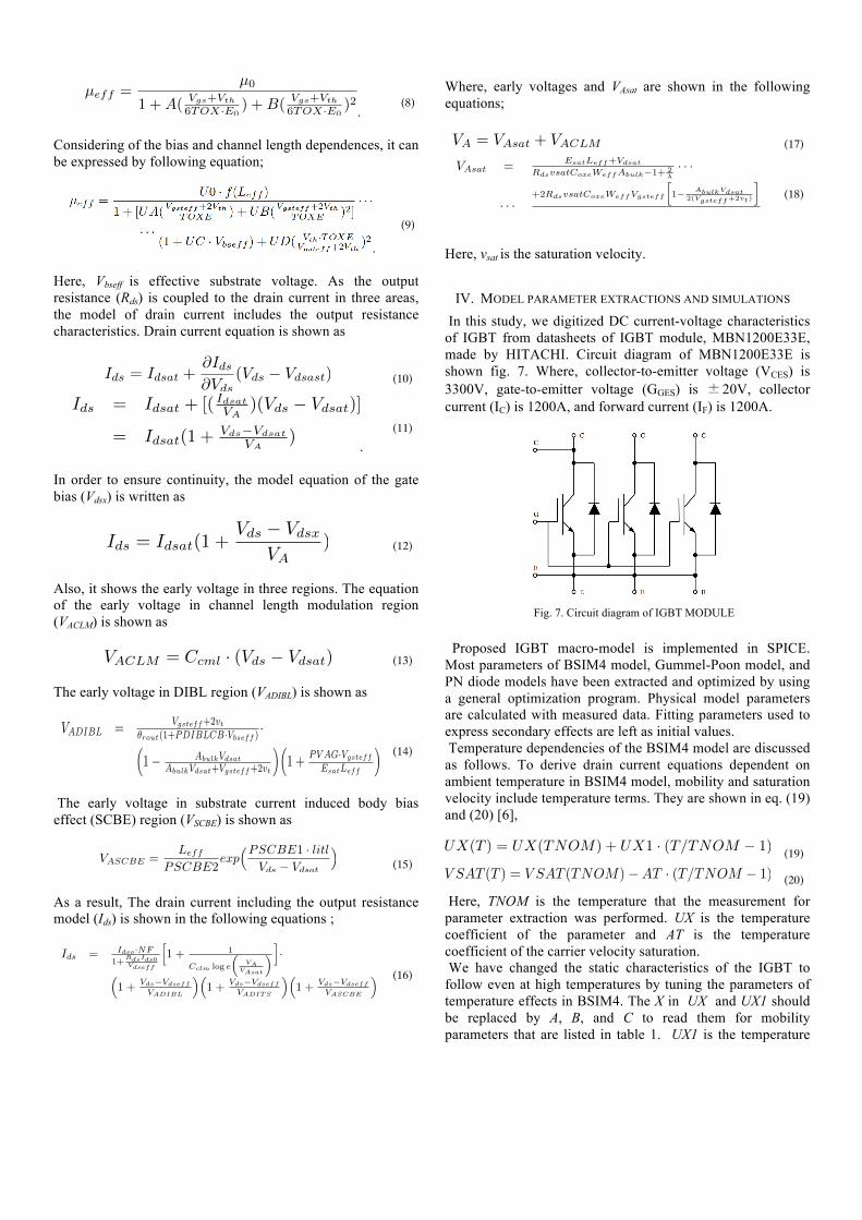
Simulation results of the conventional macro-model [3] are shown in Fig. 5.
Fig. 5. Anode DC current comparison of the conventional IGBT model [3]
The result shows that the simulation accuracy of the static DC output characteristics is not enough to use it for any circuit designs. We would like to propose a macro-model of IGBT (named as A-IGBT model) to improve the accuracy of static simulations, which includes IGBT itself, and free-wheel diodes.
III. MACRO-MODEL DEVELOPMENT A-IGBT model is shown in Fig. 6 [4]. Two pn diodes are connected in parallel, in addition to the equivalent circuit of conventional IGBT. These pn diodes are applied to control the backward breakdown voltage of the n--layer and to simulate the forward current characteristic of the free-wheel diode. Other role is to represent turn-off transient simulations operated by junction capacitances of pn diodes. By connecting two different pn junction diode models in parallel, the parameters of each diode can be set, independently. Thus, they increase the flexibility of the slope

Fig. 6. Proposed IGBT macro model (A-IGBT)
at current-voltage characteristic curve. In addition, we use the BSIM4 model to simulate the DMOS characteristics. To represent the carrier mobility behavior, UCBMOS level 3 supports linear mobility reduction with an analytical equation whose number of parameters is only one. BSIM4 supports four kind of mobility equation options to represent vertical and horizontal fields effects. Thus, it is possible to more accurately represent the current drift model for the model. Moreover, saturation region model of BSIM4 can be classified into three regions of the channel length modulation effect, DIBL (Drain Induced Barrier Lowering) effect and the hot electron effect the output resistance. Therefore, the output resistance can be accurately represented by BSIM4. Although A-IGBT model has a very simple equivalent circuit, it is suitable for the device operation mechanisms.
To explain the model equation of the Carrier mobility and the output resistance in BSIM4 [5], model parameter is shown in table Ⅰ.
TABLE I. BSIM4 MODEL PARAMETERS RELATED TO CARREIER MOBILITY AND OUTPUT RESISTANCE
Parameter Name Description TOX Gate oxide thickness U0 Carrier mobility UA First order factor of mobility
degradation UB Second order factor of mobility
degradation UC Substrate effect factor of
mobility degradation UD Coulomb scattering mobility
degradation factor TOXE Electrical gate oxide thickness
Vt Thermal voltage
Vgsteff Smoothing function to the gate bias
PCLM Channel length modulation parameter
PDIBLCB Body bias coefficient of DIBL effect on Rout
Abulk Substrate charge effect PVAG Gate depending parameter of
early voltage Leff Effective channel length
DROUT Channel-length dependence of DIBL effect on Rout
PSCBE1 First substrate current induced body-effect parameter
PSCBE2 Second substrate current induced body-effect parameter
NF Number of gate fingers Carrier mobility in BSIM4 is modeled based on the electric field in the vertical direction. Carriers affected by the effective electric field (Eeff) in the inversion layer are shown in the following equations ;
. (4)
Here, QB is substrate charge, Qinv is inversion charge and εsv is silicon permittivity. This equation can be written by the model parameters and the voltage as
. (5)
Where, Vgs is gate source voltage, and Vth is threshold voltage. The effective carrier mobility (µeff) and effective electric field are associated as follows;
. (6)
Where, v is a coefficient of the electric field ratio. This equation derives as a quadratic equation by series expansion as
. (7)
Where, A and B are the constants that occur in the series expansion. The following equation is obtained by substituting (7) to (5) as
Eeff =QB + Qinv
2
✏si
Eeff⇠=
Vgs + Vth
6TOX
µeff =µ0
1 + (Eeff
E0)v
µeff =µ0
1 +A(Eeff
E0) +B(Eeff
E0)2
. (8)
Considering of the bias and channel length dependences, it can be expressed by following equation;
.
(9)
Here, Vbseff is effective substrate voltage. As the output resistance (Rds) is coupled to the drain current in three areas, the model of drain current includes the output resistance characteristics. Drain current equation is shown as
(10)
. (11)
In order to ensure continuity, the model equation of the gate bias (Vdsx) is written as
(12)
Also, it shows the early voltage in three regions. The equation of the early voltage in channel length modulation region (VACLM) is shown as
(13) The early voltage in DIBL region (VADIBL) is shown as
(14)
The early voltage in substrate current induced body bias effect (SCBE) region (VSCBE) is shown as
(15)
As a result, The drain current including the output resistance model (Ids) is shown in the following equations ;
(16)
Where, early voltages and VAsat are shown in the following equations;
(17)
(18)
Here, vsat is the saturation velocity.
IV. MODEL PARAMETER EXTRACTIONS AND SIMULATIONS In this study, we digitized DC current-voltage characteristics of IGBT from datasheets of IGBT module, MBN1200E33E, made by HITACHI. Circuit diagram of MBN1200E33E is shown fig. 7. Where, collector-to-emitter voltage (VCES) is 3300V, gate-to-emitter voltage (GGES) is ±20V, collector current (IC) is 1200A, and forward current (IF) is 1200A.
Fig. 7. Circuit diagram of IGBT MODULE
Proposed IGBT macro-model is implemented in SPICE.
Most parameters of BSIM4 model, Gummel-Poon model, and PN diode models have been extracted and optimized by using a general optimization program. Physical model parameters are calculated with measured data. Fitting parameters used to express secondary effects are left as initial values. Temperature dependencies of the BSIM4 model are discussed as follows. To derive drain current equations dependent on ambient temperature in BSIM4 model, mobility and saturation velocity include temperature terms. They are shown in eq. (19) and (20) [6],
(19)
(20)
Here, TNOM is the temperature that the measurement for parameter extraction was performed. UX is the temperature coefficient of the parameter and AT is the temperature coefficient of the carrier velocity saturation. We have changed the static characteristics of the IGBT to follow even at high temperatures by tuning the parameters of temperature effects in BSIM4. The X in UX and UX1 should be replaced by A, B, and C to read them for mobility parameters that are listed in table 1. UX1 is the temperature
µeff =µ0
1 +A( Vgs+Vth
6TOX·E0) +B( Vgs+Vth
6TOX·E0)2
Ids = Idsat +@Ids@Vds
(Vds � Vdsast)
Ids = Idsat + [( IdsatVA
)(Vds � Vdsat)]
= Idsat(1 +Vds�Vdsat
VA)
Ids
= Idsat
(1 +Vds
� Vdsx
VA
)
VACLM = Ccml · (Vds � Vdsat)
VADIBL = Vgsteff
+2vt
✓rout
(1+PDIBLCB·Vbseff
) ·⇣1� A
bulk
Vdsat
Abulk
Vdsat
+Vgsteff
+2vt
⌘⇣1 + PV AG·V
gsteff
Esat
Leff
⌘
VASCBE =Leff
PSCBE2exp
⇣PSCBE1 · litlVds � Vdsat
⌘
Ids = Idso
·NF
1+
R
ds
I
ds0V
dseff
h1 + 1
Cclm
log e
⇣V
A
V
Asat
⌘i·
⇣1 + V
ds
�Vdseff
VADIBL
⌘⇣1 + V
ds
�Vdseff
VADITS
⌘⇣1 + V
ds
�Vdseff
VASCBE
⌘
VA = VAsat + VACLM
VAsat = Esat
Leff
+Vdsat
Rds
vsatCoxe
Weff
Abulk
�1+ 2�
· · ·
· · ·+2R
ds
vsatCoxe
Weff
Vgsteff
h1� A
bulk
V
dsat
2(Vgsteff
+2vt
)
i
UX(T ) = UX(TNOM) + UX1 · (T/TNOM � 1)
V SAT (T ) = V SAT (TNOM)�AT · (T/TNOM � 1)
coefficient of the parameter UX. These temperature parameters have been extracted and optimized with drain current measurements dependent on drain and gate voltages in linear and saturation regions at 25 and 125 Celsius. Parameters related to mobility and saturation velocity are shown in table Ⅰ and Ⅱ.
TABLE II. BSIM4 MODEL PARAMETERS RELATED TO TEMPERATURE DEPENDENCE ON MOBILITY
Parameter Name Value
U0 400 [m/V] UA 2.29×10⁻⁹ [m/V] UB 5.87×10⁻¹⁹ [m2/V2] UC 0 [m/V2] UA1 10.0×-9 [m/V] UB1 -2.61×10⁻¹⁸ [m2/V2] UC1 -40.0×10⁻¹² [m2/V2]
TABLE III. BSIM4 MODEL PARAMETERS RELATED TO TEMPERATURE DEPENDENCE OF SATURATION VELOCITY
Parameter Name Value
VSAT 8.00×10⁴ [m/s] AT 2.30×10⁴ [m/s]
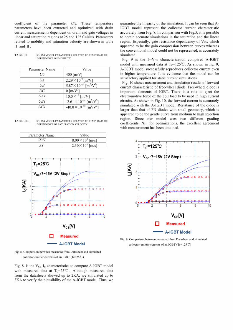
Fig. 8. Comparison between measured from Datasheet and simulated
collector-emitter currents of an IGBT (Tc=25℃) Fig. 8. is the VCE-IC characteristics to compare A-IGBT model with measured data at TC=25℃. Although measured data from the datasheets showed up to 2KA, we simulated up to 3KA to verify the plausibility of the A-IGBT model. Thus, we
guarantee the linearity of the simulation. It can be seen that A-IGBT model represent the collector current characteristic accurately from Fig. 8. In comparison with Fig.5, it is possible to obtain accurate simulations in the saturation and the linear region. Especially, gate resistance dependency of VCE, which appeared to be the gain compression between curves whereas the conventional model could not be represented, is accurately simulated.
Fig. 9 is the IC-VCE characterization compared A-IGBT model with measured data at TC=125℃. As shown in fig. 9, A-IGBT model successfully reproduces collector current even in higher temperature. It is evidence that the model can be satisfactory applied for static current simulations.
Fig. 10 shows measurement and simulation results of forward current characteristic of free-wheel diode. Free-wheel diode is important elements of IGBT. There is a role to eject the electromotive force of the coil load to be used in high current circuits. As shown in Fig. 10, the forward current is accurately simulated with the A-IGBT model. Resistance of the diode is larger than that of PN diodes with small geometry, which is appeared to be the gentle curve from medium to high injection region. Since our model uses two different grading coefficients, NF, for optimizations, the excellent agreement with measurement has been obtained.
Fig. 9. Comparison between measured from Datasheet and simulated
collector-emitter currents of an IGBT (Tc=125℃)
37
37
ICE vs VCE≉ᛶ䝰䝕䝸䞁䜾⤖ᯝ
A-IGBT Model
VCE[V] VCE[V]
Measured䠄䝕䞊䝍䝅䞊䝖䜘䜚䠅
IC[KA] TC=25Υ
VGE䠖7~15V 䠄2V Step䠅
TC=125Υ
VGE䠖7~15V 䠄2V Step䠅
37
37
I CE
vs V
CE≉
ᛶ䝰䝕䝸䞁䜾⤖
ᯝ
A-I
GB
T M
od
el
VC
E[V
]V
CE[V
]
Me
as
ure
d䠄䝕䞊䝍䝅䞊䝖䜘䜚
䠅
I C[K
A]
TC=
25Υ
VG
E䠖7
~1
5V
䠄2
V S
tep䠅
TC=
125Υ
VG
E䠖7
~1
5V
䠄2
V S
tep䠅
37
37
ICE vs VCE≉ᛶ䝰䝕䝸䞁䜾⤖ᯝ
A-IGBT Model
VCE[V] VCE[V]
Measured䠄䝕䞊䝍䝅䞊䝖䜘䜚䠅
IC[KA] TC=25Υ
VGE䠖7~15V 䠄2V Step䠅
TC=125Υ
VGE䠖7~15V 䠄2V Step䠅
14年5月29日木曜日
37
37
ICE vs VCE≉ᛶ䝰䝕䝸䞁䜾⤖ᯝ
A-IGBT Model
VCE[V] VCE[V]
Measured䠄䝕䞊䝍䝅䞊䝖䜘䜚䠅
IC[KA] TC=25Υ
VGE䠖7~15V 䠄2V Step䠅
TC=125Υ
VGE䠖7~15V 䠄2V Step䠅
37
37
I CE
vs V
CE≉
ᛶ䝰䝕䝸䞁䜾⤖
ᯝ
A-I
GB
T M
od
el
VC
E[V
]V
CE[V
]
Me
as
ure
d䠄䝕䞊䝍䝅䞊䝖䜘䜚
䠅
I C[K
A]
TC=
25Υ
VG
E䠖7
~1
5V
䠄2
V S
tep䠅
TC=
125Υ
VG
E䠖7
~1
5V
䠄2
V S
tep䠅
37
37
ICE vs VCE≉ᛶ䝰䝕䝸䞁䜾⤖ᯝ
A-IGBT Model
VCE[V] VCE[V]
Measured䠄䝕䞊䝍䝅䞊䝖䜘䜚䠅
IC[KA] TC=25Υ
VGE䠖7~15V 䠄2V Step䠅
TC=125Υ
VGE䠖7~15V 䠄2V Step䠅
14年5月29日木曜日

Fig. 10. Measurement from Datasheet and simulation results of forward
current of free-wheel diode
V. CONCLUSION This paper proposed a new IGBT macro-model for SPICE simulators and extractions of the high precision model parameters by using the DC I-V measurements. BSIM4 model is applied for the core DMOS structure to represent the drift current and output resistance models, accurately. Simulation results with the proposed macro-model represent the static characteristics, accurately. In addition, this simulation can be accurately represented static characteristics of the IGBT at high temperature by extracting model parameters of temperature effects related to mobility and saturation velocity. We are going to continue to develop the capacitance model of IGBT, then, complete our A-IGBT model by verifying the switching characteristics.
REFERENCES [1] PSpice Reference Guide, Cadance, 2000. [2] S. M. Sze, “Physics of Semiconductor”, 2nd, Wiley Inter-science, 1981. [3] 0. Apeldoom, S. Schmitt, and R.W. De Doncker: “An Electrical Model
of a NPT-IGBT Including Transient Temperature Effects Realized with PSpice Device Equations Modeling”, IEEE Catalog, No. 97TH8280 pp.223-228 (1997).
[4] Masaki Kazumi, Hitoshi Aoki, Yukiko Arai, Ramin Khatami, Shunichiro Todoroki, Takuya Totsuka, Fumitaka Abe, Haruo Kobayashi “Study of High Accuracy IGBT Macro-Model”, IEEJ Technical Meeting in Tochigi, Gunma Area, Kiryu (Feb.2014)
[5] Hitoshi Aoki, Masanori Shimasue, Yasuo Kawahara: CMOS Modeling technology, Maruzen Publishing, 2006. Hitoshi Aoki, Masanori Shimasue, Yasuo Kawahara CMOS Modeling technology, Maruzen Publishing, 2006.
[6] Mohan V. Dunga, Xuemei (Jane) Xi, Jin He, Weidong Liu, Kanyu M. Cao, Xiaodong Jin, Jeff J. Ou, Mansun Chan, Ali M. Niknejad, Chenming Hu, BSIM4.6.0 MOSFET Model – User’s Manual, 2006
39
1/27/2014
39
䝎䜲䜸䞊䝗㡰᪉㟁ὶ≉ᛶ䝰䝕䝸䞁䜾⤖ᯝ
Measured䠄䝕䞊䝍䝅䞊䝖䜘䜚䠅
A-IGBT Model
Forward Current [KA]
Forward Voltage [V]
TC=25Υ
TC=125Υ
39
1/27/2014 39
䝎䜲䜸䞊䝗㡰
᪉
㟁ὶ
≉ᛶ
䝰䝕䝸䞁䜾⤖
ᯝ
Mea
sure
d䠄䝕䞊䝍䝅䞊䝖䜘䜚
䠅
A-I
GB
T M
od
el
Fo
rwar
d C
urr
ent
[KA
]
Fo
rwar
d V
olt
age
[V]
TC=
25Υ
TC=
125Υ
37
37
ICE vs VCE≉ᛶ䝰䝕䝸䞁䜾⤖ᯝ
A-IGBT Model
VCE[V] VCE[V]
Measured䠄䝕䞊䝍䝅䞊䝖䜘䜚䠅
IC[KA] TC=25Υ
VGE䠖7~15V 䠄2V Step䠅
TC=125Υ
VGE䠖7~15V 䠄2V Step䠅
14年5月29日木曜日