xc83x ds - 北京晶川电子技术发展有限公司 · characteristics. with respect to any...
TRANSCRIPT

Data SheetV1.1 2010-11
Microcontrol lers
XC835/8368-Bit Single-Chip Microcontroller
Edition 2010-11Published byInfineon Technologies AG81726 Munich, Germany© 2010 Infineon Technologies AGAll Rights Reserved.
Legal DisclaimerThe information given in this document shall in no event be regarded as a guarantee of conditions or characteristics. With respect to any examples or hints given herein, any typical values stated herein and/or any information regarding the application of the device, Infineon Technologies hereby disclaims any and all warranties and liabilities of any kind, including without limitation, warranties of non-infringement of intellectual property rights of any third party.
InformationFor further information on technology, delivery terms and conditions and prices, please contact the nearest Infineon Technologies Office (www.infineon.com).
WarningsDue to technical requirements, components may contain dangerous substances. For information on the types in question, please contact the nearest Infineon Technologies Office.Infineon Technologies components may be used in life-support devices or systems only with the express written approval of Infineon Technologies, if a failure of such components can reasonably be expected to cause the failure of that life-support device or system or to affect the safety or effectiveness of that device or system. Life support devices or systems are intended to be implanted in the human body or to support and/or maintain and sustain and/or protect human life. If they fail, it is reasonable to assume that the health of the user or other persons may be endangered.

Data SheetV1.1 2010-11
Microcontrol lers
XC835/8368-Bit Single-Chip Microcontroller

XC835/836
Data Sheet V1.1, 2010-11
XC835/836 Data Sheet
Revision History: V1.1 2010-11Previous Versions: V 1.0Page Subjects (major changes since last revision)Page 3 Automotive variants and package type are updated.Page 21 Chip identification number for the new variant is updated.Page 46 The thermal characteristics of TSSOP-28-9 package for Automotive profile
is added.Page 49 The package outline of TSSOP-28-9 package for Automotive profile is
added.
We Listen to Your CommentsIs there any information in this document that you feel is wrong, unclear or missing?Your feedback will help us to continuously improve the quality of this document.Please send your proposal (including a reference to this document) to:[email protected]

XC835/836
Table of Contents
Data Sheet 1 V1.1, 2010-11
1 Summary of Features . . . . . . . . . . . . . . . . . . . . . . . . . . . . . . . . . . . . . . . . 1
2 General Device Information . . . . . . . . . . . . . . . . . . . . . . . . . . . . . . . . . . . 52.1 Block Diagram . . . . . . . . . . . . . . . . . . . . . . . . . . . . . . . . . . . . . . . . . . . . . . . 52.2 Logic Symbol . . . . . . . . . . . . . . . . . . . . . . . . . . . . . . . . . . . . . . . . . . . . . . . . 62.3 Pin Configuration . . . . . . . . . . . . . . . . . . . . . . . . . . . . . . . . . . . . . . . . . . . . . 72.4 Pin Definitions and Functions . . . . . . . . . . . . . . . . . . . . . . . . . . . . . . . . . . . 92.5 Memory Organization . . . . . . . . . . . . . . . . . . . . . . . . . . . . . . . . . . . . . . . . 182.6 JTAG ID . . . . . . . . . . . . . . . . . . . . . . . . . . . . . . . . . . . . . . . . . . . . . . . . . . . 202.7 Chip Identification Number . . . . . . . . . . . . . . . . . . . . . . . . . . . . . . . . . . . . 21
3 Electrical Parameters . . . . . . . . . . . . . . . . . . . . . . . . . . . . . . . . . . . . . . . 223.1 General Parameters . . . . . . . . . . . . . . . . . . . . . . . . . . . . . . . . . . . . . . . . . 223.1.1 Parameter Interpretation . . . . . . . . . . . . . . . . . . . . . . . . . . . . . . . . . . . . 223.1.2 Absolute Maximum Rating . . . . . . . . . . . . . . . . . . . . . . . . . . . . . . . . . . . 233.1.3 Operating Condition . . . . . . . . . . . . . . . . . . . . . . . . . . . . . . . . . . . . . . . . 243.2 DC Parameters . . . . . . . . . . . . . . . . . . . . . . . . . . . . . . . . . . . . . . . . . . . . . 253.2.1 Input/Output Characteristics . . . . . . . . . . . . . . . . . . . . . . . . . . . . . . . . . 253.2.2 Supply Threshold Characteristics . . . . . . . . . . . . . . . . . . . . . . . . . . . . . 283.2.3 ADC Characteristics . . . . . . . . . . . . . . . . . . . . . . . . . . . . . . . . . . . . . . . 293.2.3.1 ADC Conversion Timing . . . . . . . . . . . . . . . . . . . . . . . . . . . . . . . . . . 323.2.3.2 Out of Range Comparator Characteristics . . . . . . . . . . . . . . . . . . . . . 323.2.4 Flash Memory Parameters . . . . . . . . . . . . . . . . . . . . . . . . . . . . . . . . . . 333.2.5 Power Supply Current . . . . . . . . . . . . . . . . . . . . . . . . . . . . . . . . . . . . . . 353.3 AC Parameters . . . . . . . . . . . . . . . . . . . . . . . . . . . . . . . . . . . . . . . . . . . . . 383.3.1 Testing Waveforms . . . . . . . . . . . . . . . . . . . . . . . . . . . . . . . . . . . . . . . . 383.3.2 Output Rise/Fall Times . . . . . . . . . . . . . . . . . . . . . . . . . . . . . . . . . . . . . 393.3.3 Oscillator Timing and Wake-up Timing . . . . . . . . . . . . . . . . . . . . . . . . . 403.3.4 On-Chip Oscillator Characteristics . . . . . . . . . . . . . . . . . . . . . . . . . . . . . 413.3.5 SSC Timing . . . . . . . . . . . . . . . . . . . . . . . . . . . . . . . . . . . . . . . . . . . . . . 433.3.5.1 SSC Master Mode Timing . . . . . . . . . . . . . . . . . . . . . . . . . . . . . . . . . 433.3.5.2 SSC Slave Mode Timing . . . . . . . . . . . . . . . . . . . . . . . . . . . . . . . . . . 443.3.6 SPD Timing . . . . . . . . . . . . . . . . . . . . . . . . . . . . . . . . . . . . . . . . . . . . . . 45
4 Package and Quality Declaration . . . . . . . . . . . . . . . . . . . . . . . . . . . . . . 464.1 Package Parameters . . . . . . . . . . . . . . . . . . . . . . . . . . . . . . . . . . . . . . . . . 464.2 Package Outline . . . . . . . . . . . . . . . . . . . . . . . . . . . . . . . . . . . . . . . . . . . . 474.3 Quality Declaration . . . . . . . . . . . . . . . . . . . . . . . . . . . . . . . . . . . . . . . . . . 50
Table of Contents

XC835/836
Table of Contents
Data Sheet 2 V1.1, 2010-11

XC835/836
Summary of Features
Data Sheet 1 V1.1, 2010-11
1 Summary of FeaturesThe XC835/836 has the following features:• High-performance XC800 Core
– compatible with standard 8051 processor– two clocks per machine cycle architecture (for memory access without wait state)– two data pointers
• On-chip memory– 8 Kbytes of Boot ROM, Library ROM and User routines– 256 bytes of RAM– 256 bytes of XRAM– 4/8 Kbytes of Flash (includes memory protection strategy)
• I/O port supply at 2.5 V - 5.5 V and core logic supply at 2.5 V (generated byembedded voltage regulator)
Figure 1 XC835/836 Functional Units
• Power-on reset generation• Brownout detection for IO supply and core logic supply• 48 MHz on-chip OSC for clock generation
– Loss-of-Clock detection(more features on next page)
Port 0
Port 1
Port 2
XC800 Core
UART
ADC10-bit
8-channel
Boot ROM8K Bytes
XRAM256 Bytes
RAM256 Bytes
On-Chip Debug Support
Timer 016-bit
Timer 116-bit
Timer 216-bit
Watchdog Timer
SSC8/4K Bytes Flash
Capture/Compare Unit16-bit
Compare Unit16-bit
8-bit Digital I/O
6-bit Digital I/O
8-bit Digital/Analog Input
IIC
MDU
LED and Touch Sense Controller
Real-Time Clock
Port 3
CORDIC
3-bit Digital I/O

XC835/836
Summary of Features
Data Sheet 2 V1.1, 2010-11
Features: (continued)• Power saving modes
– idle mode– power-down mode with wake-up capability via real-time clock event– clock gating control to each peripheral
• Programmable 16-bit Watchdog Timer (WDT) running on independent oscillator withprogrammable window feature for refresh operation and warning prior to overflow
• Three general purpose I/O ports– 4 high current I/O– 2 high sink I/O– Up to 25 pins as digital I/O– Up to 8 pins as digital/analog input
• Up to 8 channels, 10-bit A/D Converter– support up to 7 differential input channel– results filtering by data reduction or digital low-pass filter, for up to 13-bit results
• Up to 8 channels, Out of range comparator• Three 16-bit timers
– Timer 0 and Timer 1 (T0 and T1)– Timer 2 (T2)
• Real-time clock with 32.768 kHz crystal pad• 16-bit Vector Computer for Field-Oriented Control (FOC)
– Multiplication/Division Unit (MDU) for arithmetic calculation– CORDIC Unit for trigonometric calculation
• Capture and Compare unit for PWM signal generation (CCU6)• A full-duplex or half-duplex serial interface (UART)• Synchronous serial channel (SSC)• Inter-IC (IIC) serial interface• LED and Touch-sense Controller (LEDTSCU)• Software libraries to support fixed-point control and EEPROM emulation• On-chip debug support via single pin DAP interface (SPD)• Packages:
– PG-DSO-24– PG-TSSOP-28
• Temperature range TA:– SAF (-40 to 85 °C)

XC835/836
Summary of Features
Data Sheet 3 V1.1, 2010-11
XC835/836 Variant DevicesThe XC835/836 product family features devices with different configurations, programmemory sizes, packages options and temperature profiles, to offer cost-effectivesolutions for different application requirements. The list of XC835/836 device configurations are summarized in Table 1. The type ofpackages available are DSO-24 for XC835 and TSSOP-28 for XC836.
Table 2 shows the device sales type available, based on above device.
As this document refers to all the derivatives, some description may not apply to aspecific product. For simplicity, all versions are referred to by the term XC835/836throughout this document.
Table 1 Device ConfigurationDevice Name MDU and CORDIC Module LEDTSCU ModuleXC835/836 No NoXC835/836M Yes NoXC835/836T No YesXC835/836MT Yes Yes
Table 2 Device ProfileSales Type Device
TypeProgram Memory (Kbytes)
Temp-erature Profile (°C)
Package Type
Quality Profile
SAF-XC835MT-2FGI Flash 8 -40 to 85 PG-DSO-24-1 IndustrialSAF-XC836-2FRI Flash 8 -40 to 85 PG-TSSOP-28-1 IndustrialSAF-XC836T-2FRI Flash 8 -40 to 85 PG-TSSOP-28-1 IndustrialSAF-XC836M-2FRI Flash 8 -40 to 85 PG-TSSOP-28-1 IndustrialSAF-XC836M-1FRI Flash 4 -40 to 85 PG-TSSOP-28-1 IndustrialSAF-XC836MT-2FRI Flash 8 -40 to 85 PG-TSSOP-28-1 IndustrialSAF-XC836MT-2FRA Flash 8 -40 to 85 PG-TSSOP-28-9 AutomotiveSAF-XC836MT-1FRA Flash 4 -40 to 85 PG-TSSOP-28-9 AutomotiveSAK-XC836MT-2FRA Flash 8 -40 to 125 PG-TSSOP-28-9 AutomotiveSAK-XC836MT-1FRA Flash 4 -40 to 125 PG-TSSOP-28-9 Automotive

XC835/836
Summary of Features
Data Sheet 4 V1.1, 2010-11
Ordering InformationThe ordering code for Infineon Technologies microcontrollers provides an exactreference to the required product. This ordering code identifies:• The derivative itself, i.e. its function set, the temperature range, and the supply
voltage• The package and the type of deliveryFor the available ordering codes for the XC835/836, please refer to your responsiblesales representative or your local distributor.
XC835/836
General Device Information
Data Sheet 5 V1.1, 2010-11
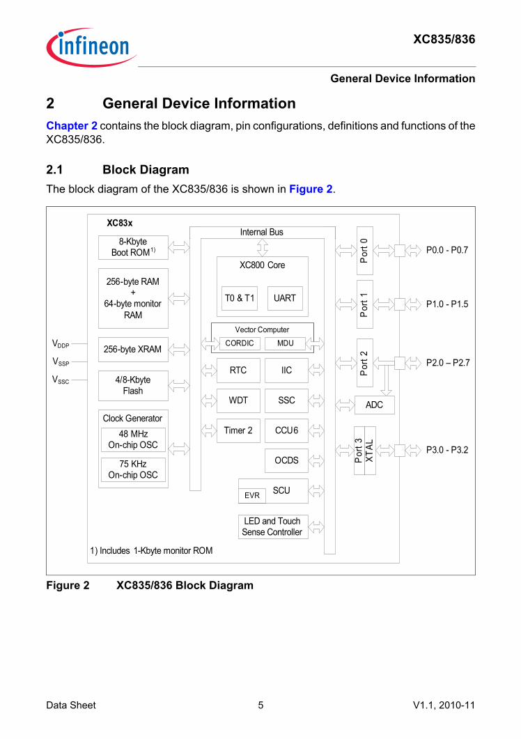
2 General Device InformationChapter 2 contains the block diagram, pin configurations, definitions and functions of theXC835/836.
2.1 Block DiagramThe block diagram of the XC835/836 is shown in Figure 2.
Figure 2 XC835/836 Block Diagram
Por
t 0P
ort 1
LED and Touch Sense Controller
8-Kbyte Boot ROM1)
256-byte RAM+
64-byte monitor RAM
256-byte XRAM
4/8-Kbyte Flash
XC800 Core
T0 & T1 UART
1) Includes 1-Kbyte monitor ROM
P0.0 - P0.7
P1.0 - P1.5
Clock Generator48 MHz
On-chip OSC
Internal Bus
VDDP
VSSP
VSSC
XC83x
WDT SSC
IICRTC
CCU6
ADC
Por
t 2 P2.0 – P2.7P
ort 3 P3.0 - P3.2
XTAL
75 KHz On-chip OSC
Timer 2
SCUEVR
CORDIC MDU
Vector Computer
OCDS
XC835/836
General Device Information
Data Sheet 6 V1.1, 2010-11
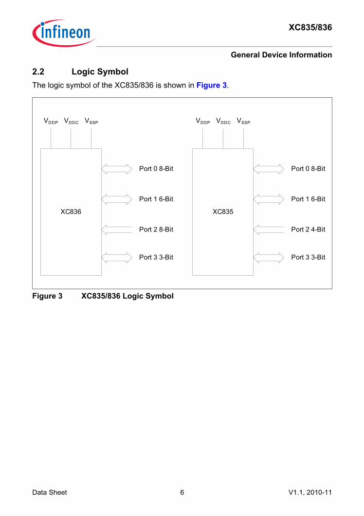
2.2 Logic SymbolThe logic symbol of the XC835/836 is shown in Figure 3.
Figure 3 XC835/836 Logic Symbol
XC836
VDDP VSSPVDDC
Port 0 8-Bit
Port 1 6-Bit
Port 2 8-Bit
XC835
VDDP VSSPVDDC
Port 0 8-Bit
Port 1 6-Bit
Port 2 4-Bit
Port 3 3-Bit Port 3 3-Bit
XC835/836
General Device Information
Data Sheet 7 V1.1, 2010-11
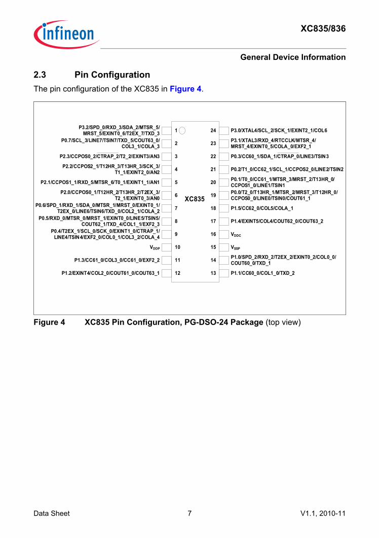
2.3 Pin ConfigurationThe pin configuration of the XC835 in Figure 4.
Figure 4 XC835 Pin Configuration, PG-DSO-24 Package (top view)
1
2
3
4
5
6
7
8
9
10
11
12
14
13
23
22
21
20
19
18
17
16
15
24
XC835
P1.0/SPD_2/RXD_2/T2EX_2/EXINT0_2/COL0_0/COUT60_0/TXD_1
P1.4/EXINT5/COL4/COUT62_0/COUT63_2
P0.6/SPD_1/RXD_1/SDA_0/MTSR_1/MRST_0/EXINT0_1/T2EX_0/LINE6/TSIN6/TXD_0/COL2_1/COLA_2
P0.5/RXD_0/MTSR_0/MRST_1/EXINT0_0/LINE5/TSIN5/COUT62_1/TXD_4/COL1_1/EXF2_3
P1.3/CC61_0/COL3_0/CC61_0/EXF2_2
P0.1/T0_0/CC61_1/MTSR_3/MRST_2/T13HR_0/CCPOS1_0/LINE1/TSIN1
P0.2/T1_0/CC62_1/SCL_1/CCPOS2_0/LINE2/TSIN2
P3.0/XTAL4/SCL_2/SCK_1/EXINT2_1/COL6
P3.1/XTAL3/RXD_4/RTCCLK/MTSR_4/MRST_4/EXINT0_5/COLA_0/EXF2_1
P3.2/SPD_0/RXD_3/SDA_2/MTSR_5/MRST_5/EXINT0_6/T2EX_7/TXD_3
P1.5/CC62_0/COL5/COLA_1
P0.0/T2_0/T13HR_1/MTSR_2/MRST_3/T12HR_0/CCPOS0_0/LINE0/TSIN0/COUT61_1
VDDP VSSP
VDDC
P2.1/CCPOS1_1/RXD_5/MTSR_6/T0_1/EXINT1_1/AN1
P1.2/EXINT4/COL2_0/COUT61_0/COUT63_1
P2.2/CCPOS2_1/T12HR_3/T13HR_3/SCK_3/T1_1/EXINT2_0/AN2
P0.7/SCL_3/LINE7/TSIN7/TXD_5/COUT63_0/COL3_1/COLA_3
P1.1/CC60_0/COL1_0/TXD_2
P2.0/CCPOS0_1/T12HR_2/T13HR_2/T2EX_3/T2_1/EXINT0_3/AN0
P0.4/T2EX_1/SCL_0/SCK_0/EXINT1_0/CTRAP_1/LINE4/TSIN4/EXF2_0/COL0_1/COL3_2/COLA_4
P0.3/CC60_1/SDA_1/CTRAP_0/LINE3/TSIN3P2.3/CCPOS0_2/CTRAP_2/T2_2/EXINT3/AN3

XC835/836
General Device Information
Data Sheet 8 V1.1, 2010-11
The pin configuration of the XC836 in Figure 5.
Figure 5 XC836 Pin Configuration, PG-TSSOP-28 Package (top view)
1
2
3
4
5
6
7
8
9
10
11
12
13
14
18
17
16
15
27
26
25
24
23
22
21
20
19
28
XC836
P2.6/SCK_2/EXINT6/AN6
P2.5/T12HR_7/T13HR_7/AN5
P2.4/T12HR_5/T13HR_5/T2_3/AN4
P1.4/EXINT5/COL4/COUT62_0/COUT63_2
P0.6/SPD_1/RXD_1/SDA_0/MTSR_1/MRST_0/EXINT0_1/T2EX_0/LINE6/TSIN6/TXD_0/COL2_1/COLA_2
P0.5/RXD_0/MTSR_0/MRST_1/EXINT0_0/LINE5/TSIN5/COUT62_1/TXD_4/COL1_1/EXF2_3
P0.1/T0_0/CC61_1/MTSR_3/MRST_2/T13HR_0/CCPOS1_0/LINE1/TSIN1
P0.2/T1_0/CC62_1/SCL_1/CCPOS2_0/LINE2/TSIN2
P3.0/XTAL4/SCL_2/SCK_1/EXINT2_1/COL6
P3.1/XTAL3/RXD_4/RTCCLK/MTSR_4/MRST_4/EXINT0_5/COLA_0/EXF2_1
P3.2/SPD_0/RXD_3/SDA_2/MTSR_5/MRST_5/EXINT0_6/T2EX_7/TXD_3
P1.5/CC62_0/COL5/COLA_1
P0.0/T2_0/T13HR_1/MTSR_2/MRST_3/T12HR_0/CCPOS0_0/LINE0/TSIN0/COUT61_1
VDDP VSSP
VDDC
P2.1/CCPOS1_1/RXD_5/MTSR_6/T0_1/EXINT1_1/AN1
P2.2/CCPOS2_1/T12HR_3/T13HR_3/SCK_3/T1_1/EXINT2_0/AN2
P0.7/SCL_3/LINE7/TSIN7/TXD_5/COUT63_0/COL3_1/COLA_3P2.7/RXD_6/T2EX_6/MTSR_7/EXINT0_4/AN7
P2.3/CCPOS0_2/CTRAP_2/T2_2/EXINT3/AN3
P2.0/CCPOS0_1/T12HR_2/T13HR_2/T2EX_3/T2_1/EXINT0_3/AN0
P0.4/T2EX_1/SCL_0/SCK_0/EXINT1_0/CTRAP_1/LINE4/TSIN4/EXF2_0/COL0_1/COL3_2/COLA_4
P0.3/CC60_1/SDA_1/CTRAP_0/LINE3/TSIN3
P1.0/SPD_2/RXD_2/T2EX_2/EXINT0_2/COL0_0/COUT60_0/TXD_1P1.3/CC61_0/COL3_0/CC61_0/EXF2_2
P1.2/EXINT4/COL2_0/COUT61_0/COUT63_1 P1.1/CC60_0/COL1_0/TXD_2

XC835/836
General Device Information
Data Sheet 9 V1.1, 2010-11
2.4 Pin Definitions and FunctionsThe functions and default states of the XC835/836 external pins are provided in Table 3.
Table 3 Pin Definitions and Functions for XC835/836Symbol Pin
NumberTSSOP28/DS024
Type Reset State
Function
P0 I/O Port 0Port 0 is a bidirectional general purpose I/O port. It can be used as alternate functions for LEDTSCU, Timer 0, 1 and 2, SSC, CCU6, IIC, SPD and UART.
P0.0 21/19 Hi-Z T2_0 Timer 2 InputT13HR_1 CCU6 Timer 13 Hardware Run
InputMTSR_2 SSC Master Transmit Output/
Slave Receive InputMRST_3 SSC Master Receive InputT12HR_0 CCU6 Timer 12 Hardware Run
InputCCPOS0_0 CCU6 Hall Input 0TSIN0 Touch-sense Input 0LINE0 LED Line 0COUT61_1 Output of Capture/Compare
Channel 1

XC835/836
General Device Information
Data Sheet 10 V1.1, 2010-11
P0.1 22/20 Hi-Z T0_0 Timer 0 InputCC61_1 Input/Output of Capture/Compare
channel 1MTSR_3 SSC Slave Receive InputMRST_2 SSC Master Receive Input/
Slave Transmit OutputT13HR_0 CCU6 Timer 13 Hardware Run
InputCCPOS1_0 CCU6 Hall Input 1TSIN1 Touch-sense Input 1LINE1 LED Line 1
P0.2 23/21 Hi-Z T1_0 Timer 1 InputCC62_1 Input/Output of Capture/Compare
channel 2SCL_1 IIC Clock LineCCPOS2_0 CCU6 Hall Input 2TSIN2 Touch-sense Input 2LINE2 LED Line 2
P0.3 24/22 Hi-Z CC60_1 Input/Output of Capture/Compare channel 0
SDA_1 IIC Data LineCTRAP_0 CCU6 Trap InputTSIN3 Touch-sense Input 3LINE3 LED Line 3
Table 3 Pin Definitions and Functions for XC835/836 (cont’d)
Symbol Pin NumberTSSOP28/DS024
Type Reset State
Function

XC835/836
General Device Information
Data Sheet 11 V1.1, 2010-11
P0.4 11/9 PD T2EX_1 Timer 2 External Trigger InputSCK_0 SSC Clock Input/OutputSCL_0 IIC Clock LineCTRAP_1 CCU6 Trap InputEXINT1_0 External Interrupt Input 1TSIN4 Touch-sense Input 4LINE4 LED Line 4EXF2_0 Timer 2 Overflow FlagCOL0_1 LED Column 0COL3_2 LED Column 3COLA_4 LED Column A
P0.5 10/8 Hi-Z RXD_0 UART Receive InputMTSR_0 SSC Master Transmit Output/
Slave Receive InputMRST_1 SSC Master Receive InputEXINT0_0 External Interrupt Input 0TSIN5 Touch-sense Input 5LINE5 LED Line 5COUT62_1 Output of Capture/Compare
Channel 2TXD_4 UART Transmit OutputCOL1_1 LED Column 1EXF2_3 Timer 2 Overflow Flag
Table 3 Pin Definitions and Functions for XC835/836 (cont’d)
Symbol Pin NumberTSSOP28/DS024
Type Reset State
Function

XC835/836
General Device Information
Data Sheet 12 V1.1, 2010-11
P0.6 9/7 PU SPD_1 SPD Input/OutputRXD_1 UART Receive InputSDA_0 IIC Data LineMTSR_1 SSC Slave Receive InputMRST_0 SSC Master Receive Input/
Slave Transmit OutputEXINT0_1 External Interrupt Input 0T2EX_0 Timer 2 External Trigger InputTSIN6 Touch-sense Input 6LINE6 LED Line 6TXD_0 UART Transmit OutputCOL2_1 LED Column 2COLA_2 LED Column A
P0.7 28/2 Hi-Z SCL_3 IIC Clock LineTSIN7 Touch-sense Input 7LINE7 LED Line 7TXD_5 UART Transmit Output/
2-wire UART BSL Transmit OutputCOUT63_0 Output of Capture/Compare
Channel 3COL3_1 LED Column 3COLA_3 LED Column A
P1 I/O Port 1Port 1 is a bidirectional general purpose I/O port. It can be used as alternate functions for CCU6, LEDTSCU, SPD, UART and Timer 2
Table 3 Pin Definitions and Functions for XC835/836 (cont’d)
Symbol Pin NumberTSSOP28/DS024
Type Reset State
Function

XC835/836
General Device Information
Data Sheet 13 V1.1, 2010-11
P1.0 16/14 Hi-Z SPD_2 SPD Input/OutputRXD_2 UART Receive InputT2EX_2 Timer 2 External Trigger InputEXINT0_2 External Interrupt Input 0COL0_0 LED Column 0COUT60_0 Output of Capture/Compare
Channel 0TXD_1 UART Transmit Output
P1.1 15/13 Hi-Z CC60_0 Input/Output of Capture/Compare channel 0
COL1_0 LED Column 1TXD_2 UART Transmit Output
P1.2 14/12 Hi-Z EXINT4 External Interrupt Input 4COL2_0 LED Column 2COUT61_0 Output of Capture/Compare
channel 1COUT63_1 Output of Capture/Compare
channel 3P1.3 13/11 Hi-Z CC61_0 Input/Output of Capture/Compare
channel 1COL3_0 LED Column 3EXF2_2 Timer 2 Overflow Flag
P1.4 19/17 Hi-Z EXINT5 External Interrupt Input 5COL4 LED Column 4COUT62_0 Output of Capture/Compare
channel 2COUT63_2 Output of Capture/Compare
channel 3
Table 3 Pin Definitions and Functions for XC835/836 (cont’d)
Symbol Pin NumberTSSOP28/DS024
Type Reset State
Function

XC835/836
General Device Information
Data Sheet 14 V1.1, 2010-11
P1.5 20/18 Hi-Z CC62_0 Input/Output of Capture/Compare channel 2
COL5 LED Column 5COLA_1 LED Column A
P2 I Port 2Port 2 is a general purpose input-only port. It can be used as inputs for A/D Converter and out of range comparator, CCU6, Timer 2, SSC and UART.
P2.0 8/6 Hi-Z CCPOS0_1 CCU6 Hall Input 0T12HR_2 CCU6 Timer 12 Hardware Run
InputT13HR_2 CCU6 Timer 13 Hardware Run
InputT2EX_3 Timer 2 External Trigger InputT2_1 Timer 2 InputEXINT0_3 External Interrupt Input 0AN0 Analog Input 0 /
Out of range comparator channel 0P2.1 7/5 Hi-Z CCPOS1_1 CCU6 Hall Input 1
RXD_5 UART Receive InputMTSR_6 SSC Slave Receive InputT0_1 Timer 0 InputEXINT1_1 External Interrupt Input 1AN1 Analog Input 1 /
Out of range comparator channel 1
Table 3 Pin Definitions and Functions for XC835/836 (cont’d)
Symbol Pin NumberTSSOP28/DS024
Type Reset State
Function

XC835/836
General Device Information
Data Sheet 15 V1.1, 2010-11
P2.2 6/4 Hi-Z CCPOS2_1 CCU6 Hall Input 2T12HR_3 CCU6 Timer 12 Hardware Run
InputT13HR_3 CCU6 Timer 13 Hardware Run
InputSCK_3 SSC Clock Input/OutputT1_1 Timer 1 InputEXINT2_0 External Interrupt Input 2AN2 Analog Input 2 /
Out of range comparator channel 2P2.3 5/3 Hi-Z CCPOS0_2 CCU6 Hall Input 0
CTRAP_2 CCU6 Trap InputT2_2 Timer 2 InputEXINT3 External Interrupt Input 3AN3 Analog Input 3 /
Out of range comparator channel 3P2.4 4/- Hi-Z T12HR_5 CCU6 Timer 12 Hardware Run
InputT13HR_5 CCU6 Timer 13 Hardware Run
InputT2_3 Timer 2 InputAN4 Analog Input 4 /
Out of range comparator channel 4P2.5 3/- Hi-Z T12HR_7 CCU6 Timer 12 Hardware Run
InputT13HR_7 CCU6 Timer 13 Hardware Run
InputAN5 Analog Input 5 /
Out of range comparator channel 5
Table 3 Pin Definitions and Functions for XC835/836 (cont’d)
Symbol Pin NumberTSSOP28/DS024
Type Reset State
Function

XC835/836
General Device Information
Data Sheet 16 V1.1, 2010-11
P2.6 2/- Hi-Z SCK_2 SSC Clock Input/OutputEXINT6 External Interrupt Input 6AN6 Analog Input 6 /
Out of range comparator channel 6P2.7 1/- Hi-Z RXD_6 UART Receive Input
T2EX_6 Timer 2 External Trigger InputMTSR_7 SSC Slave Receive InputEXINT0_4 External Interrupt Input 0AN7 Analog Input 7 /
Out of range comparator channel 7P3 I/O Port 3
Port 3 is a bidirectional general purpose I/O port. It can be used as alternate functions for IIC, LEDTSCU, UART, Timer 2, SSC, SPD and 32.768 kHz crystal pad.
P3.0 26/24 PU SCL_2 IIC Clock LineSCK_1 SSC Clock Input/OutputEXINT2_1 External Interrupt Input 2COL6 LED Column 6XTAL4 32.768 kHz External Oscillator
Output
Table 3 Pin Definitions and Functions for XC835/836 (cont’d)
Symbol Pin NumberTSSOP28/DS024
Type Reset State
Function

XC835/836
General Device Information
Data Sheet 17 V1.1, 2010-11
P3.1 25/23 PU RXD_4 UART Receive InputRTCCLK RTC External Clock InputMTSR_4 SSC Master Transmit Output/
Slave Receive InputMRST_4 SSC Master Receive InputEXINT0_5 External Interrupt Input 0COLA_0 LED Column AXTAL3 32.768 kHz External oscillator
InputEXF2_1 Timer 2 Overflow Flag
P3.2 27/1 PU SPD_0 SPD Input/OutputRXD_3 UART Receive Input/
UART BSL Receive InputSDA_2 IIC Data LineMTSR_5 SSC Slave Receive InputMRST_5 SSC Master Receive Input/
Slave Transmit OutputEXINT0_6 External Interrupt Input 0T2EX_7 Timer 2 External Trigger InputTXD_3 UART Transmit Output/
1-wire UART BSL Transmit OutputVDDP 12/10 – – I/O Port Supply (2.5 V - 5.5 V)VDDC 18/16 – – Core Supply Monitor (2.5 V)VSSP/VSSC
17/15 – – I/O Port Ground/Core Supply Ground
Table 3 Pin Definitions and Functions for XC835/836 (cont’d)
Symbol Pin NumberTSSOP28/DS024
Type Reset State
Function

XC835/836
General Device Information
Data Sheet 18 V1.1, 2010-11
2.5 Memory OrganizationThe XC835/836 CPU operates in the following five address spaces:• 8 Kbytes of Boot ROM, Library ROM and User routines • 256 bytes of internal RAM • 256 bytes of XRAM
(XRAM can be read/written as program memory or external data memory)• A 128-byte Special Function Register area• 4/8 Kbytes of Flash Figure 6 illustrates the memory address spaces of the 4 Kbyte Flash devices. Figure 7illustrates the memory address spaces of the 8 Kbyte Flash devices.
Figure 6 Memory Map of XC835/836 with 4 Kbytes of Flash memory
0000H
1000H
F000H
C000H
E000H
F100H
FFFF H
Flash Bank 04 KBytes
Boot ROM8 KBytes
XRAM256 Bytes F000H
F100H
0000H
FFFF H
Special Function Registers
IndirectAddress
DirectAddress
80H
FFH
00H
Code Space External Data Space Internal Data Space
Internal RAM
Memory Map User Mode
XRAM256 Bytes
7FHInternal RAM
B000H
Flash Bank 04 KBytes 1)
A000H
In Debug Mode, this 64-byte address area is replaced by a 64-byte Monitor RAM.
40H
1) Physically one 4-Kbyte Flash bank, mapped to both address range .

XC835/836
General Device Information
Data Sheet 19 V1.1, 2010-11
Figure 7 Memory Map of XC835/836 with 8 Kbytes of Flash memory
0000H
1000H
F000H
C000H
E000H
F100H
FFFF H
Flash Bank 04 KBytes
Boot ROM8 KBytes
XRAM256 Bytes F000H
F100H
0000H
FFFF H
Special Function Registers
IndirectAddress
DirectAddress
80H
FFH
00H
Code Space External Data Space Internal Data Space
Internal RAM
Memory Map User Mode
XRAM256 Bytes
7FHInternal RAM
B000H
Flash Bank 14 KBytes 1)
2000H
A000H
In Debug Mode, this 64-byte address area is replaced by a 64-byte Monitor RAM.
40H
Flash Bank 14 KBytes 1)
1) Physically one 4-Kbyte Flash bank, mapped to both address range . Flash Bank 1 is only available in 8-Kbyte Flash Variant .2) User BSL Flash sector is only available in 8-Kbyte Flash Variant .
User BSL Flash Sector 64 Bytes2)
FF40H
FF80H
XC835/836
General Device Information
Data Sheet 20 V1.1, 2010-11
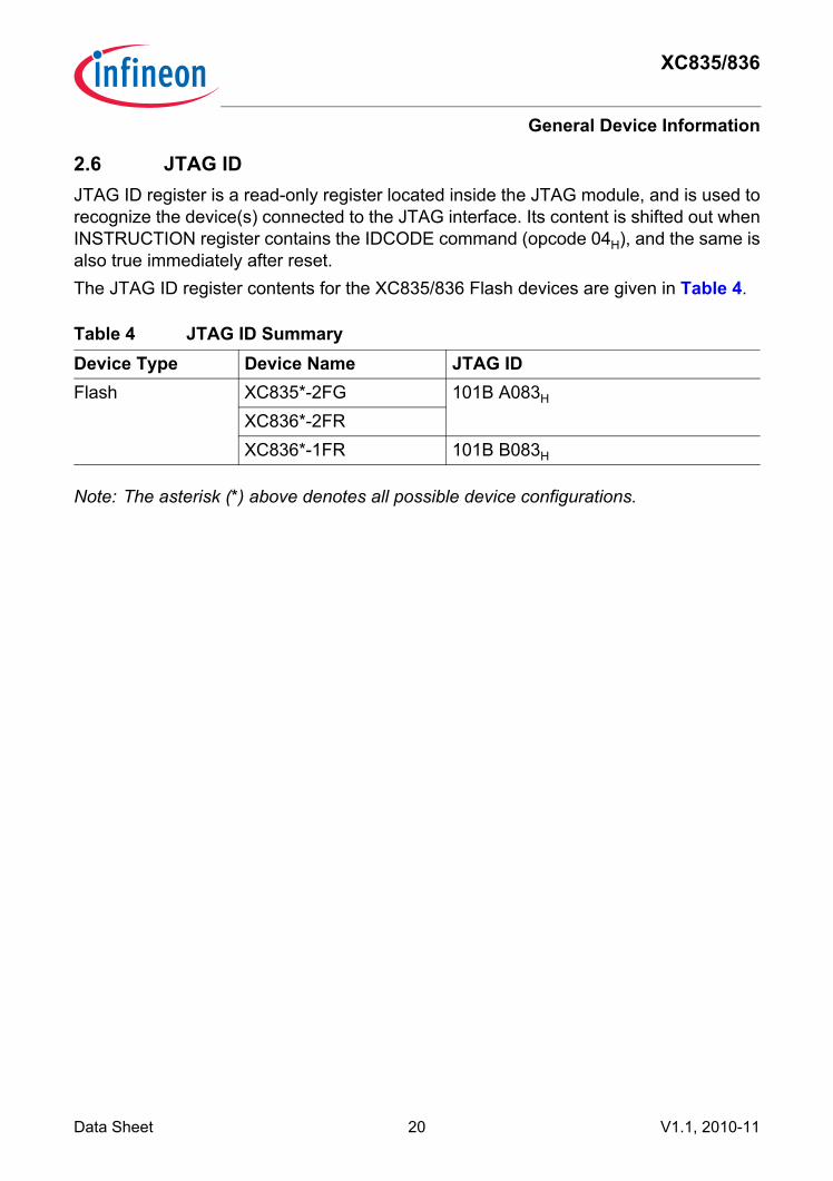
2.6 JTAG IDJTAG ID register is a read-only register located inside the JTAG module, and is used torecognize the device(s) connected to the JTAG interface. Its content is shifted out whenINSTRUCTION register contains the IDCODE command (opcode 04H), and the same isalso true immediately after reset.The JTAG ID register contents for the XC835/836 Flash devices are given in Table 4.
Note: The asterisk (*) above denotes all possible device configurations.
Table 4 JTAG ID SummaryDevice Type Device Name JTAG IDFlash XC835*-2FG 101B A083H
XC836*-2FRXC836*-1FR 101B B083H

XC835/836
General Device Information
Data Sheet 21 V1.1, 2010-11
2.7 Chip Identification NumberThe XC835/836 identity (ID) register is located at Page 1 of address B3H. The value ofID register is 59H. However, for easy identification of product variants, the ChipIdentification Number, which is an unique number assigned to each product variant, isavailable. The differentiation is based on the product and variant type information.Two methods are provided to read a device’s Chip Identification number:• In-application subroutine, GET_CHIP_INFO• Boot-loader (BSL) mode ATable 5 lists the Chip Identification numbers of XC835/836 device variants.
Table 5 Chip Identification NumberProduct Variant Chip Identification NumberXC835MT-2FG 59080001H
XC836-2FR 59080060H
XC836T-2FR 59080040H
XC836M-2FR 59080020H
XC836M-1FR 59080120H
XC836MT-2FR 59080000H
XC836MT-1FR 59080100H

XC835/836
Electrical Parameters
Data Sheet 22 V1.1, 2010-11
3 Electrical ParametersChapter 3 provides the characteristics of the electrical parameters which areimplementation-specific for the XC835/836.
3.1 General ParametersThe general parameters are described here to aid the users in interpreting theparameters mainly in Section 3.2 and Section 3.3.
3.1.1 Parameter InterpretationThe parameters listed in this section represent partly the characteristics of theXC835/836 and partly its requirements on the system. To aid interpreting the parameterseasily when evaluating them for a design, they are indicated by the abbreviations in the“Symbol” column:• CC
– These parameters indicate Controller Characteristics, which are distinctivefeatures of the XC835/836 and must be regarded for a system design.
• SR– These parameters indicate System Requirements, which must be provided by the
microcontroller system in which the XC835/836 is designed in.

XC835/836
Electrical Parameters
Data Sheet 23 V1.1, 2010-11
3.1.2 Absolute Maximum RatingMaximum ratings are the extreme limits to which the XC835/836 can be subjected towithout permanent damage.
Note: Stresses above those listed under “Absolute Maximum Ratings” may causepermanent damage to the device. This is a stress rating only and functionaloperation of the device at these or any other conditions above those indicated inthe operational sections of this specification is not implied. Exposure to absolutemaximum rating conditions for extended periods may affect device reliability.During absolute maximum rating overload conditions (VIN > VDDP or VIN < VSS) thevoltage on VDDP pin with respect to ground (VSS) must not exceed the valuesdefined by the absolute maximum ratings.
Table 6 Absolute Maximum Rating ParametersParameter Symbol Limit Values Unit Notes
Min. Max.Ambient temperature TA -40 125 °C under biasStorage temperature TST -65 150 °C –Junction temperature TJ -40 150 °C under biasVoltage on power supply pin with respect to VSS
VDDP -0.5 6 V
Maximum current per pin for P1[3:0]
IM -115 115 mA
Input current on any pin during overload condition
IIN -10 10 mA
Absolute sum of all input currents during overload condition
Σ|IIN| – 50 mA
XC835/836
Electrical Parameters
Data Sheet 24 V1.1, 2010-11
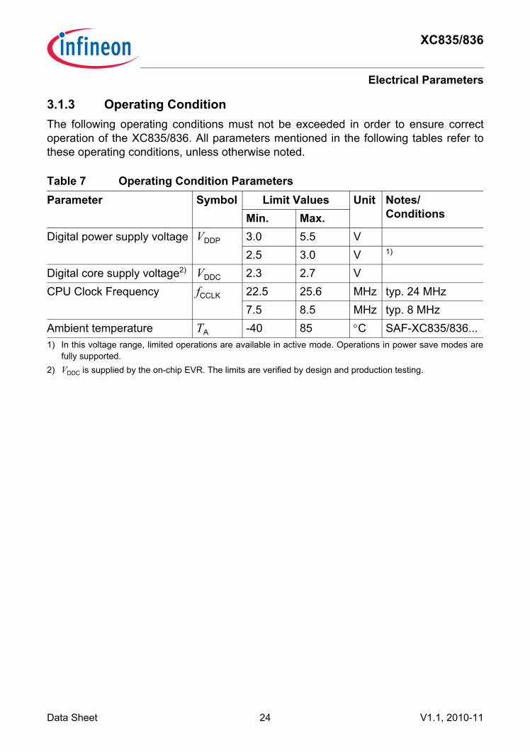
3.1.3 Operating ConditionThe following operating conditions must not be exceeded in order to ensure correctoperation of the XC835/836. All parameters mentioned in the following tables refer tothese operating conditions, unless otherwise noted.
Table 7 Operating Condition ParametersParameter Symbol Limit Values Unit Notes/
ConditionsMin. Max.Digital power supply voltage VDDP 3.0 5.5 V
2.5 3.0 V 1)
1) In this voltage range, limited operations are available in active mode. Operations in power save modes arefully supported.
Digital core supply voltage2)
2) VDDC is supplied by the on-chip EVR. The limits are verified by design and production testing.
VDDC 2.3 2.7 VCPU Clock Frequency fCCLK 22.5 25.6 MHz typ. 24 MHz
7.5 8.5 MHz typ. 8 MHzAmbient temperature TA -40 85 °C SAF-XC835/836...

XC835/836
Electrical Parameters
Data Sheet 25 V1.1, 2010-11
3.2 DC ParametersThe electrical characteristics of the DC Parameters are detailed in this section.
3.2.1 Input/Output CharacteristicsTable 8 provides the characteristics of the input/output pins of the XC835/836.
Table 8 Input/Output Characteristics (Operating Conditions apply)Parameter Symbol Limit Values Unit Test Conditions
Min. Max.Output low voltage on port pins (all except P1)
VOLP CC – 1.0 V IOL = 25 mA (5 V)IOL = 13 mA (3.3 V)
– 0.4 V IOL = 10 mA (5 V)IOL = 5 mA (3.3 V)
Output low voltage on P1[3:0]
VOLP1 CC – 1.0 V IOL = 50 mA (5 V)IOL = 25 mA (3.3 V)
– 0.32 V IOL = 20 mA (5 V)– 0.4 V IOL = 10 mA (3.3 V )
Output low voltage on P1[5:4]
VOLP2 CC – 1.0 V IOL = 50 mA (5 V)IOL = 25 mA (3.3 V)
– 0.4 V IOL = 20 mA (5 V)IOL = 10 mA (3.3 V)
Output high voltage on port pins(all except P1)
VOHP CC VDDP - 1.0
– V IOH = -15 mA (5 V)IOH = -8 mA (3.3 V )
VDDP - 0.4
– V IOH = -5 mA (5 V)IOH = -2.5 mA (3.3 V)
Output high voltage on P1[3:0]
VOHP1 CC VDDP - 0.32
– V IOH = -20 mA (5 V)
VDDP - 1.0
– V IOH = -25 mA (3.3 V)
VDDP - 0.4
– V IOH = -10 mA (3.3 V)
Output high voltage on P1[5:4]
VOHP2 CC VDDP - 1.0
– V IOH = -30 mA (5 V)IOH = -16 mA (3.3 V)
VDDP - 0.4
– V IOH = -10 mA (5 V)IOH =- 5 mA (3.3 V)

XC835/836
Electrical Parameters
Data Sheet 26 V1.1, 2010-11
Input low voltage on port pins
VILP SR – 0.3 × VDDP
V CMOS Mode (5 & 3.3 V)
Input high voltage on port pins
VIHP SR 0.7 × VDDP
– V CMOS Mode(5 V & 3.3 V)
Input Hysteresis1) HYS CC 0.08 × VDDP
– V CMOS Mode (5 V)
0.03 × VDDP
– V CMOS Mode (3.3 V)
0.01 × VDDP
– V CMOS Mode (2.5 V)
Pull-up current IPUP SR – -20 µA VIH,min (5 V)-150 – µA VIL,max (5 V)– -5 µA VIH,min (3.3 V)-100 – µA VIL,max (3.3 V)
Pull-down current IPDP SR – 20 µA VIL,max (5 V)150 – µA VIH,min (5 V)– 5 µA VIL,max (3.3 V)100 – µA VIH,min (3.3 V)
Input leakage current on port pins2)
(all except P1)
IOZP CC -1 1 µA 0 < VIN < VDDP,TA ≤ 125 °C
Input leakage current on P1[3:0]2)
IOZP1 CC -3 3 µA 0 < VIN < VDDP,TA ≤ 125 °C
Input leakage current on P1[5:4]2)
IOZP2 CC -2 2 µA 0 < VIN < VDDP,TA ≤ 125 °C
Overcurrent threshold per pin for P1[3:0]3)
|IOCP1| SR 60 115 mA VDDP = 5 V
Overload current on any pin
IOVP SR -5 5 mA 4)
Absolute sum of overload currents
Σ|IOV| SR – 25 mA 4)
Table 8 Input/Output Characteristics (Operating Conditions apply) (cont’d)
Parameter Symbol Limit Values Unit Test ConditionsMin. Max.

XC835/836
Electrical Parameters
Data Sheet 27 V1.1, 2010-11
Voltage on any pin during VDDP power off
VPO SR – 0.3 V 5)
Maximum current per pin (excluding P1, VDDP and VSS)
IMP SR -15 25 mA –
Maximum current per pin for P1[3:0]
IMP1A SR -50 50 mA –
Maximum current per pin for P1[5:4]
IMP1B SR -30 50 mA –
Maximum current into VDDP
IMVDDP SR – 130 mA 4)
Maximum current out of VSS
IMVSS SR – 130 mA 4)
1) Not subjected to production test, verified by design/characterization. Hysteresis is implemented to avoid metastable states and switching due to internal ground bounce. It cannot be guaranteed that it suppresses switchingdue to external system noise.
2) An additional error current (IINJ) will flow if an overload current flows through an adjacent pin.3) Over current detection is available for 5V application only.4) Not subjected to production test, verified by design/characterization.5) Not subjected to production test, verified by design/characterization. However, for applications with strict low
power-down current requirements, it is mandatory that no active voltage source is supplied at any GPIO pinwhen VDDP is powered off.
Table 8 Input/Output Characteristics (Operating Conditions apply) (cont’d)
Parameter Symbol Limit Values Unit Test ConditionsMin. Max.
XC835/836
Electrical Parameters
Data Sheet 28 V1.1, 2010-11
3.2.2 Supply Threshold CharacteristicsTable 9 provides the characteristics of the supply threshold in the XC835/836.
Figure 8 Supply Threshold Parameters
Table 9 Supply Threshold Parameters (Operating Conditions apply)Parameters Symbol Limit Values Unit
Min. Typ. Max.VDDP prewarning voltage1)2)
1) Detection is enabled via SDCON register in active mode. It is automatically disabled in power down mode.Detection should be disabled for VDDP less than maximum of VDDPPW.
2) This parameter has a hysteresis of 50 mV.
VDDPPW CC 3.0 3.6 4.5 VVDDP brownout voltage in active mode2)3)
3) Detection is enabled via SDCON register. Detection must be disabled for application with VDDP less than thespecified values.
VDDPBOA CC 2.65 2.75 2.87 VVDDP brownout voltage in all power down mode2)3)
VDDPBOPD 3.0 3.6 4.5 V
VDDP system reset release voltage2)4)
4) VDDPSRR and VDDCSRR must be met before the system reset is released.
VDDPSRR CC 2.7 2.8 2.92 VVDDC prewarning voltage2)5)
5) Detection is enabled via SDCON register in active mode. It is automatically disabled in power down mode.
VDDCPW CC 2.3 2.4 2.48 VVDDC brownout voltage in active mode2) VDDCBOA CC 2.25 2.3 2.42 VVDDC brownout voltage in power down mode2) VDDCBOPD CC 1.35 1.5 1.95 VVDDC system reset release voltage2)4) VDDCSRR CC 2.28 2.3 2.47 VRAM data retention voltage VDDCRDR CC 1.1 – – V
VDDP
VDDC
VDDPPW/VDDPBOPD
VDDCSRR
VDDCPWVDDCBOA
VDDCRDR
5.0V
2.5V
VDDCBOPD
VDDPBOAVDDPSRR

XC835/836
Electrical Parameters
Data Sheet 29 V1.1, 2010-11
3.2.3 ADC CharacteristicsThe values in Table 10 are given for an analog power supply of 5.0 V. The ADC can beused with an analog power supply down to 3 V. But in this case, analog parameters mayshow a reduced performance. In the reduced voltage mode (2.5 V < VDDP < 3 V), theADC is not recommended to be used.
Table 10 ADC Characteristics (Operating Conditions apply; VDDP = 5 V; fADCI <= 12 MHz)
Parameter Symbol Limit Values Unit Test Conditions / Remarks
Min. Typ. Max.
Analog reference voltage
VAREF – VDDP – V Connect internally to VDDP
Analog reference ground
VAGND – VSSP – V Connect internally to VSSP
Alternate analog reference ground
VAGNDALT SR VSSP -0.1
– 2.51) V Connect to AN0 in differential mode, See Figure 9.
Internal voltage reference
VINTREF SR 1.19 1.23 1.28 V 4)
Analog input voltage range
VAIN SR VAGND – VAREF V –
ADC clock fADCI 8 – 16 MHz internal analog clock
Sample time tS CC (2 + INPCR0.STC) ×tADCI
µs –
Conversion time tC CC See Section 3.2.3.1 µs –Set-up time between conversions using internal voltage reference
tSETUP SR – 35 – µs 2)

XC835/836
Electrical Parameters
Data Sheet 30 V1.1, 2010-11
Total unadjusted error
TUE3) CC – – ±1 LSB8 8-bit conversion with internal reference4)
– – +4/-2 LSB10 10-bit conversion with internal reference4)5)
– – +14/-2 LSB12 12-bit conversion using the Low Pass Filter 4)
Differential Nonlinearity
EADNL CC – – +1.5/ -1 LSB 10-bit conversion4)
Integral Nonlinearity EAINL CC – – ±1.5 LSB 10-bit conversion4)
Offset EAOFF CC – +4 – LSB 10-bit conversion4)
Gain EAGAIN CC – -4 – LSB 10-bit conversion4)
Switched capacitance at an analog input
CAINSW CC – 2 3 pF 4)6)
Total capacitance at an analog input
CAINT CC – – 12 pF 4)6)
Input resistance of an analog input
RAIN CC – 1.5 2 kΩ 4)
1) 1.2 V at VDDP = 3.0 V.2) Not subject to production test, verified at CPU clock (fSCLK, CCLK ) = 8 MHz, TA = + 25 °C and VDDP = 5 V.3) TUE is tested at VAREF = VDDP = 5.0 V and CPU clock (fSCLK, CCLK ) = 8 MHz.4) Not subject to production test, verified by design/characterization.5) If a reduced positive reference voltage is used, TUE will increase. If the positive reference is reduced by a
factor of K, the TUE will increased by 1/K. Example:K = 0.8, 1/K = 1.25; 1.25 X TUE = 2.5 LSB10.6) The sampling capacity of the conversion C-Network is pre-charged to VAREF/2 before connecting the input to
the C-Network. Because of the parasitic elements, the voltage measured at ANx is lower than VAREF/2.
Table 10 ADC Characteristics (Operating Conditions apply; VDDP = 5 V; fADCI <= 12 MHz) (cont’d)
Parameter Symbol Limit Values Unit Test Conditions / Remarks
Min. Typ. Max.

XC835/836
Electrical Parameters
Data Sheet 31 V1.1, 2010-11
Figure 9 Differential like measurement with internal 1.2V voltage reference, and CH0 gnd.
Figure 10 ADC Input Circuits
AD converter
conversion control
request control
Interrupt generation
ADC kernel
resulthandling
V1.2VREF
V1.2VGND
va_altgndva_altref
AIN CH0
AIN CH1
AIN CH7
...
VSSP
REXT
Analog Input Circuitry
VAIN CEXT
ANx
CAINSW
RAIN, On
CAINT - CAINSW

XC835/836
Electrical Parameters
Data Sheet 32 V1.1, 2010-11
3.2.3.1 ADC Conversion TimingConversion time, tC = tADC × (1 + r × (3 + n + STC)), where• r = CTC + 3,• CTC = Conversion Time Control (GLOBCTR.CTC),• STC = Sample Time Control (INPCR0.STC),• n = 8 or 10 (for 8-bit and 10-bit conversion respectively),• tADC = 1 / fADC
3.2.3.2 Out of Range Comparator CharacteristicsTable 11 below shows the Out of Range Comparator characteristics.
Table 11 Out of Range Comparator Characteristics (Operating Conditions apply)
Parameter Symbol Limit Values Unit RemarksMin. Typ. Max.
DC Switching Level
VSenseDC SR 60 125 270 mV Above VDDP
DC Hysteresis VSenseHys CC 30 – – mV 1)
1) Not subject to production test, verified by design/characterization.
Pulse Width tSensePW SR 300 – – ns ANx > VDDP1)
Switching Delay tSenseSD CC – – 400 ns ANx >= VDDP + 350 mV1)
Pulse Switching Level
tSensePSL SR – 250 – mV @ 300 nsec1)
SR – 60 – mV @ 800 usec1)

XC835/836
Electrical Parameters
Data Sheet 33 V1.1, 2010-11
3.2.4 Flash Memory ParametersThe XC835/836 is delivered with all Flash sectors erased (read all zeros).The data retention time of the XC835/836’s Flash memory (i.e. the time after whichstored data can still be retrieved) depends on the number of times the Flash memory hasbeen erased and programmed.Note: Flash memory parameters are not subject to production test but verified by design
and/or characterization.
Table 12 Flash Timing Parameters (Operating Conditions apply)Parameter Symbol Limit Values Unit Remarks
Min. Typ. Max.Read access time (per byte)
tACC CC – 125 – ns
Programming time (per wordline)
tPR CC – 2.2 – ms
Erase time (one or more sectors)
tER CC – 120 – ms
Flash wait states NWSFLASH CC 0 CPU clock = 8 MHz1 CPU clock = 24 MHz
Table 13 Flash Data Retention and Endurance (Operating Conditions apply)Retention Endurance1)
1) One cycle refers to the programming of all wordlines in a sector and erasing of sector. The Flash endurancedata specified in Table 13 is valid only if the following conditions are fulfilled:- the maximum number of erase cycles per Flash sector must not exceed 100,000 cycles.- the maximum number of erase cycles per Flash bank must not exceed 300,000 cycles.- the maximum number of program cycles per Flash bank must not exceed 2,500,000 cycles.
Size Remarks20 years 1,000 cycles up to 8 Kbytes5 years 10,000 cycles 1 Kbyte2 years 70,000 cycles 512 bytes2 years 100,000 cycles 128 bytes
XC835/836
Electrical Parameters
Data Sheet 34 V1.1, 2010-11
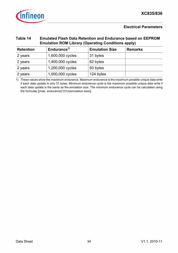
Table 14 Emulated Flash Data Retention and Endurance based on EEPROM Emulation ROM Library (Operating Conditions apply)
Retention Endurance1)
1) These values show the maximum endurance. Maximum endurance is the maximum possible unique data writeif each data update is only 31 bytes. Minimum endurance cycle is the maximum possible unique data write ifeach data update is the same as the emulation size. The minimum endurance cycle can be calculated usingthe formulae [(max. endurance)*(31)/(emulation size)].
Emulation Size Remarks2 years 1,600,000 cycles 31 bytes2 years 1,400,000 cycles 62 bytes2 years 1,200,000 cycles 93 bytes2 years 1,000,000 cycles 124 bytes

XC835/836
Electrical Parameters
Data Sheet 35 V1.1, 2010-11
3.2.5 Power Supply CurrentTable 15 provides the characteristics of the power supply current in the XC835/836.
Table 15 Power Consumption Parameters1) 2)(Operating Conditions apply)
1) The typical IDDP values are measured at TA = + 25 °C and VDDP = 5 V and 3.3 V.2) The maximum IDDC values are measured under worst case conditions (TA = + 125 °C and VDDC = 5 V).
Parameter Symbol Limit Values Unit Test ConditionTyp. Max.
Active Mode IDDPA 23 28 mA 5 V / 3.3 V 3)
3) IDDP (active mode) is measured with: CPU clock and input clock to all peripherals running at 24 MHz(CLKMODE=0).
16 20 mA 5 V / 3.3 V 4)
4) IDDP (active mode) is measured with: CPU clock and input clock to all peripherals running at 8 MHz(CLKMODE=1).
– 5 mA 2.5 V5)
5) This value is based on the maximum load capacity of EVR during VDDP = 2.5 V. Not subject to production test,verified by design/characterisation.
Idle Mode IDDPI 18 25 mA 5 V / 3.3 V 6)
6) IDDPI (idle mode) is measured with: CPU clock disabled, watchdog timer disabled, input clock to all peripheralsenabled and running at 24 MHz (CLKMODE=0).
– 5 mA 2.5 V 5)
Power Down Mode 1 IPDP1 3 5 µA TA = 25° C7)
7) IPDP1, IPDP2, IPDP3 and IPDP4 is measured at 5 V and 3.3 V with: wake-up port is programmed to be input witheither internal pull devices enabled or driven externally to ensure no floating inputs.
– 28 µA TA = 85° C7)8)9)
8) Not subject to production test, verified by design/characterisation.9) IPDP1, IPDP2, IPDP3 and IPDP4 has a maximum values of 120 uA at TA = + 125 °C.
Power Down Mode 2 IPDP2 6 8 µA TA = 25° C7)8)
– 31 µA TA = 85° C7)8)9)
Power Down Mode 3 IPDP3 5 7 µA TA = 25° C7)8)
– 30 µA TA = 85° C7)8)9)
Power Down Mode 4 IPDP4 5 7 µA TA = 25° C7)
– 30 µA TA = 85° C7)8)9)

XC835/836
Electrical Parameters
Data Sheet 36 V1.1, 2010-11
Table 16 shows the maximum active current within the device in the reduced voltagecondition of 2.5 V < VDDP < 3.0 V. The active current consumption needs to be below thespecified values as according to the VDDP voltage. If the conditions are not met, abrownout reset may be triggered.
Table 17 provides the active current consumption of some modules operating at 8 MHzactive mode, 3 V power supply at 25° C. The typical values shown are used as areference guide for device operating in reduced voltage conditions.
Table 16 Active Current Consumption in Reduced Voltage Condition VDDP 2.5 V 2.6 V 2.7 V 2.8 VMaximum active current 7 mA 13 mA 20 mA 25 mA
Table 17 Typical Active Current Consumption1) 2)
1) Modules that are controllable by programming the register PMCON1.2) Not subject to production test, verified by design/characterisation.
Active Current Consumption
Symbol Limit Values Unit Test ConditionTyp.
Baseload current3)
3) Baseload current is measured when the device is running in user mode with an endless loop in the flashmemory. All modules in register PMCON1 are disabled.
ICPUDDC 6900 µA Modules including Core, memories, UART, T0, T1 and EVR. Disable ADC analog (GLOBCTR.ANON = 0).
ADC4)
4) ADC active current is measured with: module enable, ADC analog clock at 8MHz, running in parallelconversion request in autoscan mode for 4 channels
IADCDDC 3760 µA Set PMCON1.ADC_DIS to 0 and GLOBECTR. ANON to 1
SSC5)
5) SSC active curremt is measured with: module enabled, running in loop back mode at a baud rate of 1 MBaud
ISSCDDC 460 µA Set PMCON1.SSC_DIS to 0CCU66)
6) CCU6 active current is measured with: module enabled, all timers running in 8 MHz, 6 PWM outputs aregenerated.
ICCU6DDC 3320 µA Set PMCON1.CCU_DIS to 0Timer 27) IT2DDC 200 µA Set PMCON1.T2_DIS to 0MDU8) IMDUDDC 1260 µA Set PMCON1.MDU_DIS to 0CORDIC9) ICORDICDDC 1880 µA Set PMCON1.CDC_DIS to 0LEDTSCU10) ILEDDDC 850 µA Set PMCON1.LTS_DIS to 0IIC11) IIICDDC 580 µA Set PMCON1.IIC_DIS to 0

XC835/836
Electrical Parameters
Data Sheet 37 V1.1, 2010-11
7) Timer 2 active current is measured with: module enabled, timer running in 8 MHz8) MDU active current is measured with: module enabled, division operation was performed.9) CORDIC active mode is measured with: module enabled, circular mode was selected for the calculation.10) LEDTSCU active curent is measured with: module enabled, counter running in 8 MHz.11) IIC active current is measured with: module enabled, performing a master transmit with the master clock
running at 400 KHz.

XC835/836
Electrical Parameters
Data Sheet 38 V1.1, 2010-11
3.3 AC ParametersThe electrical characteristics of the AC Parameters are detailed in this section.
3.3.1 Testing WaveformsThe testing waveforms for rise/fall time, output delay and output high impedance areshown in Figure 11, Figure 12 and Figure 13.
Figure 11 Rise/Fall Time Parameters
Figure 12 Testing Waveform, Output Delay
Figure 13 Testing Waveform, Output High Impedance
10%
90%
10%
90%
VSS
VDDP
tR tF
VDDE / 2 Test Points VDDE / 2
VSS
VDDP
VLoad + 0.1 V VOH - 0.1 VTimingReference
PointsVLoad - 0.1 V VOL - 0.1 V
XC835/836
Electrical Parameters
Data Sheet 39 V1.1, 2010-11
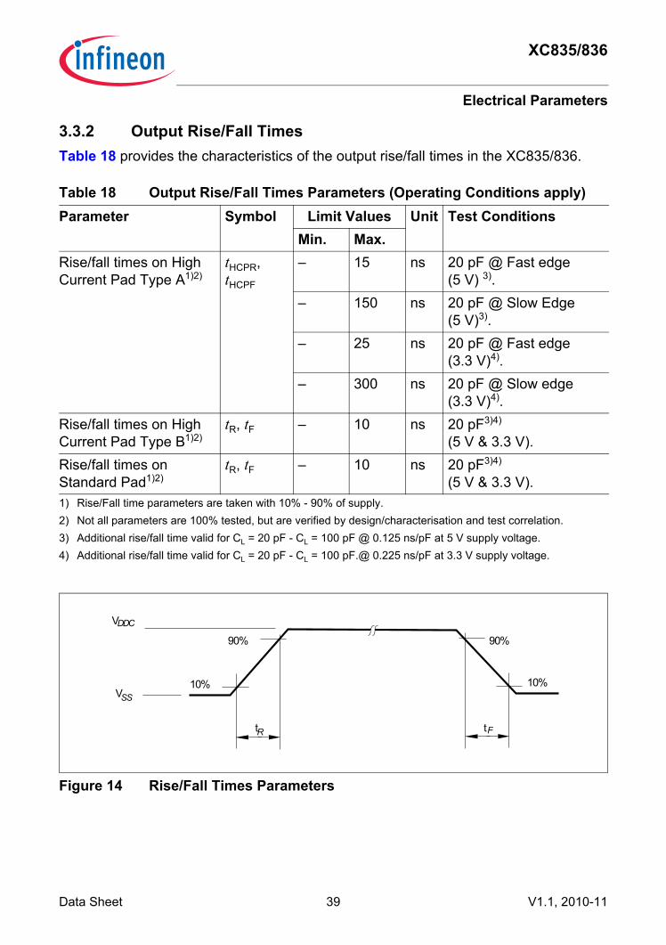
3.3.2 Output Rise/Fall TimesTable 18 provides the characteristics of the output rise/fall times in the XC835/836.
Figure 14 Rise/Fall Times Parameters
Table 18 Output Rise/Fall Times Parameters (Operating Conditions apply)Parameter Symbol Limit Values Unit Test Conditions
Min. Max.Rise/fall times on High Current Pad Type A1)2)
1) Rise/Fall time parameters are taken with 10% - 90% of supply.2) Not all parameters are 100% tested, but are verified by design/characterisation and test correlation.
tHCPR, tHCPF
– 15 ns 20 pF @ Fast edge (5 V) 3).
3) Additional rise/fall time valid for CL = 20 pF - CL = 100 pF @ 0.125 ns/pF at 5 V supply voltage.
– 150 ns 20 pF @ Slow Edge (5 V)3).
– 25 ns 20 pF @ Fast edge (3.3 V)4).
4) Additional rise/fall time valid for CL = 20 pF - CL = 100 pF.@ 0.225 ns/pF at 3.3 V supply voltage.
– 300 ns 20 pF @ Slow edge (3.3 V)4).
Rise/fall times on High Current Pad Type B1)2)
tR, tF – 10 ns 20 pF3)4) (5 V & 3.3 V).
Rise/fall times on Standard Pad1)2)
tR, tF – 10 ns 20 pF3)4) (5 V & 3.3 V).
tR
10%
90%
10%
90%
tF
VSS
VDDC

XC835/836
Electrical Parameters
Data Sheet 40 V1.1, 2010-11
3.3.3 Oscillator Timing and Wake-up TimingTable 19 provides the characteristics of the power-on reset, PLL and wake-up timings inthe XC835/836.
Table 19 Power-On Reset Wake-up Timing1) (Operating Conditions apply)
1) Not subject to production test, verified by design/characterisation.
Parameter Symbol Limit Values Unit Test ConditionsMin. Typ. Max.
48 MHz Oscillator start-up time
t48MOSCST CC – – 13 µs
75 KHz Oscillator start-up time
t75KOSCST CC – – 800 µs
32 KHz external oscillator start-up time2)
2) The external circuitry has to be optimized by the user and checked for negative resistance as recommendedand specified by the crystal supplier.
t32KOSCST CC – – 1 s
Flash initialization time tFINT CC – 160 – µs

XC835/836
Electrical Parameters
Data Sheet 41 V1.1, 2010-11
3.3.4 On-Chip Oscillator CharacteristicsTable 20 provides the characteristics of the 48 MHz oscillator in the XC835/836.
Table 20 48 MHz Oscillator Characteristics (Operating Conditions apply)Parameter Symbol Limit Values Unit Test Conditions
Min. Typ. Max.Nominal frequency fNOM CC -0.5 % 48 +0.5% MHz under nominal
conditions1) after trimming
1) Nominal condition: VDDC = 2.5 V, TA = + 25°C.
Long term frequency deviation
∆fLT CC -2.0 – 3.0 % with respect to fNOM, over lifetime and temperature (0 °C to 85 °C)
-4.5 – 4.5 % with respect to fNOM, over lifetime and temperature (-40 °C to 125 °C)
Short term frequency deviation (over VDDC)
∆fST CC -1 – 1 % with respect to fNOM, within one LIN message (< 10 ms … 100 ms)

XC835/836
Electrical Parameters
Data Sheet 42 V1.1, 2010-11
Table 21 provides the characteristics of the 75 kHz oscillator in the XC835/836.
Table 21 75 kHz Oscillator Characteristics (Operating Conditions apply)Parameter Symbol Limit Values Unit Test Conditions
Min. Typ. Max.Nominal frequency fNOM CC -1% 75 +1% KHz under nominal
conditions1) after trimming
1) Nominal condition: VDDC = 2.5 V, TA = + 25°C.
Long term frequency deviation
∆fLT CC -4.5 – 4.5 % with respect to fNOM, over lifetime and temperature (-40 °C to 125 °C)
Short term frequency deviation
∆fST CC -1.5 – 1.5 % with respect to fNOM, over VDDC

XC835/836
Electrical Parameters
Data Sheet 43 V1.1, 2010-11
3.3.5 SSC Timing
3.3.5.1 SSC Master Mode TimingTable 22 provides the SSC master mode timing in the XC835/836.
Figure 15 SSC Master Mode Timing
Table 22 SSC Master Mode Timing1) (Operating Conditions apply; CL = 50 pF)
1) Not subject to production test, verified by design/characterisation.
Parameter Symbol Limit Values UnitMin. Max.
SCLK clock period t0 CC 2 * TSSC2)
2) TSSCmin = TCPU = 1/fCPU. When fCPU = 24 MHz, t0 = 83.3 ns. TCPU is the CPU clock period.
– nsMTSR delay from SCLK t1 CC 0 3 ns
MRST set-up to SCLK t2 SR 32 – ns
MRST hold from SCLK t3 SR 0 – ns
SSC_Tmg1
SCLK1)
MTSR1)
t1 t1
MRST1)
t3Datavalid
t2
t11) This timing is based on the following setup: CON.PH = CON.PO = 0.
t0

XC835/836
Electrical Parameters
Data Sheet 44 V1.1, 2010-11
3.3.5.2 SSC Slave Mode TimingTable 23 provides the SSC slave mode timing in the XC835/836.
Figure 16 SSC Slave Mode Timing
Table 23 SSC Slave Mode Timing1) (Operating Conditions apply; CL = 50 pF)
1) Not subject to production test, verified by design/characterisation.
Parameter Symbol Limit Values UnitMin. Max.
SCLK clock period t0 SR 4 * TSSC2)
2) TSSCmin = TCPU = 1/fCPU. When fCPU = 24 MHz, t0 = 166.7 ns. TCPU is the CPU clock period.
– nsMRST delay from SCLK t1 CC 0 29 ns
MTSR set-up to SCLK t2 SR 32 – ns
MTSR hold from SCLK t3 SR 0 – ns
t2 t3
t1
SCLK1)
MTSR1)
MRST1)
t0
Data Valid
1) This timing is based on the following setup : CON.PH = CON.PO = 0.

XC835/836
Electrical Parameters
Data Sheet 45 V1.1, 2010-11
3.3.6 SPD Timing
The SPD interface will work with standard SPD tools having a sample/output clock fre-quency deviation of +/- 5% or less. For further details please refer to application note AP24004 in section SPD Timing Requirements.Note: These parameters are no subject to product test but verified by design and/or
characterization.
Note: Operating Conditions apply.

XC835/836
Package and Quality Declaration
Data Sheet 46 V1.1, 2010-11
4 Package and Quality DeclarationChapter 4 provides the information of the XC835/836 package and reliability section.
4.1 Package ParametersTable 24 provides the thermal characteristics of the packages used in XC835 andXC836 respectively.
Table 24 Thermal Characteristics of the PackagesParameter Symbol Limit Values Unit Package Types
Min. Max.Thermal resistance junction case1)
1) The thermal resistances between the case and the ambient (RTCA) , the lead and the ambient (RTLA) are to becombined with the thermal resistances between the junction and the case (RTJC), the junction and the lead(RTJL) given above, in order to calculate the total thermal resistance between the junction and the ambient(RTJA). The thermal resistances between the case and the ambient (RTCA), the lead and the ambient (RTLA)depend on the external system (PCB, case) characteristics, and are under user responsibility.The junction temperature can be calculated using the following equation: TJ=TA+RTJA × PD, where the RTJA isthe total thermal resistance between the junction and the ambient. This total junction ambient resistance RTJAcan be obtained from the upper four partial thermal resistances, by a) simply adding only the two thermal resistances (junction lead and lead ambient), or b) by taking all four resistances into account, depending on the precision needed.
RTJC CC - 30.8 K/W PG-DSO-24-1- 27.0 K/W PG-TSSOP-28-1- 20.2 K/W PG-TSSOP-28-9
Thermal resistance junction lead1)
RTJL CC - 30.5 K/W PG-DSO-24-1- 195.3 K/W PG-TSSOP-28-1- 41 K/W PG-TSSOP-28-9
XC835/836
Package and Quality Declaration
Data Sheet 47 V1.1, 2010-11
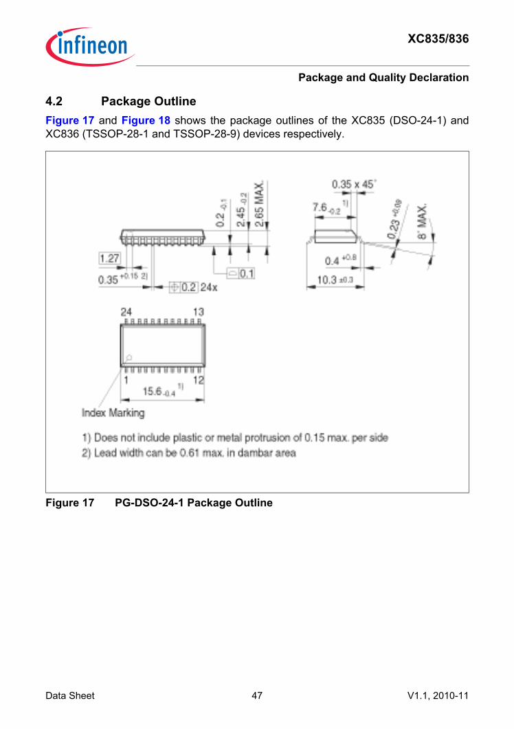
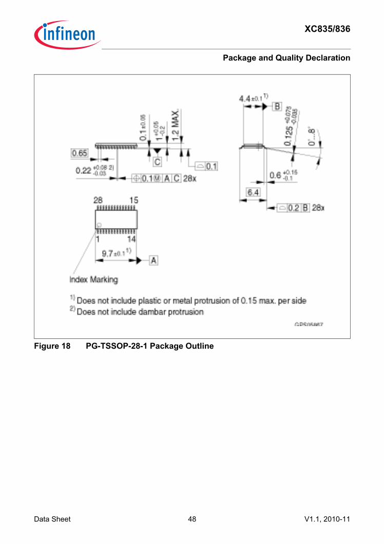
4.2 Package OutlineFigure 17 and Figure 18 shows the package outlines of the XC835 (DSO-24-1) andXC836 (TSSOP-28-1 and TSSOP-28-9) devices respectively.
Figure 17 PG-DSO-24-1 Package Outline
XC835/836
Package and Quality Declaration
Data Sheet 48 V1.1, 2010-11
Figure 18 PG-TSSOP-28-1 Package Outline
XC835/836
Package and Quality Declaration
Data Sheet 49 V1.1, 2010-11
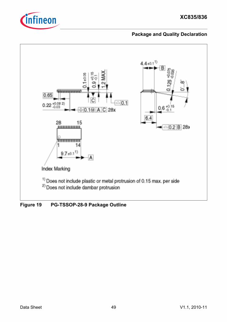
Figure 19 PG-TSSOP-28-9 Package Outline
XC835/836
Package and Quality Declaration
Data Sheet 50 V1.1, 2010-11
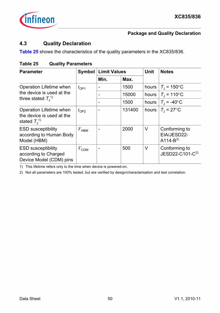
4.3 Quality DeclarationTable 25 shows the characteristics of the quality parameters in the XC835/836.
Table 25 Quality ParametersParameter Symbol Limit Values Unit Notes
Min. Max.Operation Lifetime when the device is used at the three stated TJ
1)
1) This lifetime refers only to the time when device is powered-on.
tOP1 - 1500 hours TJ = 150°C- 15000 hours TJ = 110°C- 1500 hours TJ = -40°C
Operation Lifetime when the device is used at the stated TJ
1)
tOP2 - 131400 hours TJ = 27°C
ESD susceptibility according to Human Body Model (HBM)
VHBM - 2000 V Conforming to EIA/JESD22-A114-B2)
2) Not all parameters are 100% tested, but are verified by design/characterisation and test correlation.
ESD susceptibility according to Charged Device Model (CDM) pins
VCDM - 500 V Conforming to JESD22-C101-C2)
