1-1 circuit simulation and analysis with hspice 國研院國家晶片系統設計中心 july - 2005...
Post on 18-Dec-2015
262 views
TRANSCRIPT
1-1
Circuit Simulation and Analysis with HSPICE
國研院國家晶片系統設計中心July - 2005
林棋勝
1-2
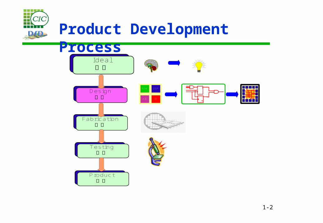
Ideal想法
Design設計
ROM DSP
I/OA/D
Vin
GND
Vref
D1
D4
Sign
ENB
A/D Converter
D
Q
QSET
CLR
Fabrication製作
Testing測試
Product產品
Product Development Process

1-3
Circuit Design Background
Circuit/System Design :
A procedure to construct a physical structure which is based on
a set of basic component, and the constructed structure will
provide a desired function at specified time/ time interval under a
given working condition.
To be DefinedInput Stimuli Output Response
1-4
FoundryManufacturing
?
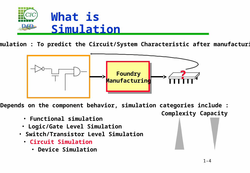
Simulation : To predict the Circuit/System Characteristic after manufacturing
Depends on the component behavior, simulation categories include :
Complexity Capacity• Functional simulation• Logic/Gate Level Simulation• Switch/Transistor Level Simulation• Circuit Simulation• Device Simulation
What is Simulation

1-5
Circuit Simulation Background
Physical Structure
Electrical characteristic
I
V
modeling
Circuit Simulation
Tool
f
gain
Behavior
+-
IN+
IN-
OUT
Circuit Structure
OUT
IN
1-6
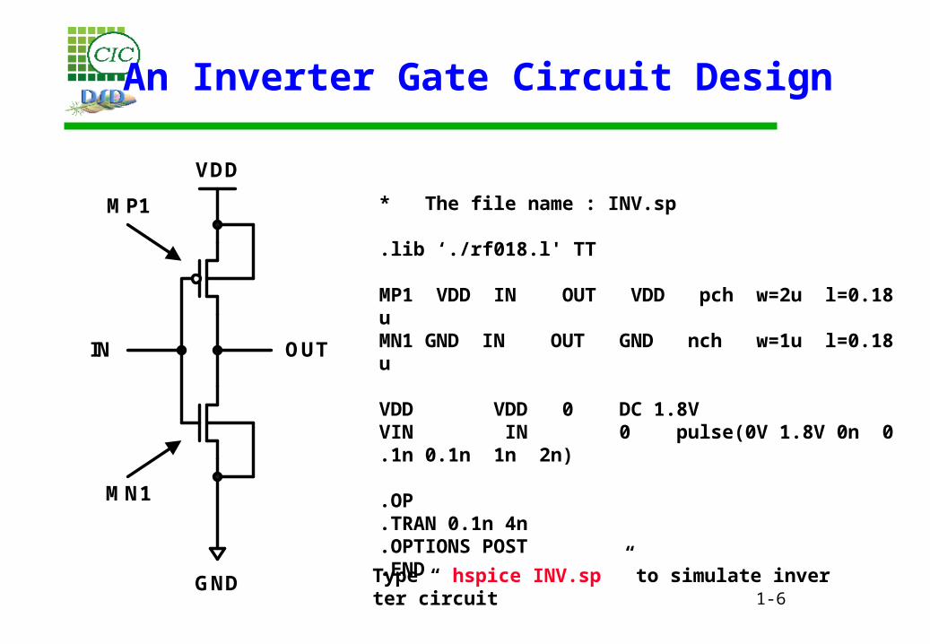
An Inverter Gate Circuit Design
* The file name : INV.sp
.lib ‘./rf018.l' TT
MP1 VDD IN OUT VDD pch w=2u l=0.18uMN1 GND IN OUT GND nch w=1u l=0.18u
VDD VDD 0 DC 1.8VVIN IN 0 pulse(0V 1.8V 0n 0.1n 0.1n 1n 2n)
.OP
.TRAN 0.1n 4n
.OPTIONS POST
.END
VDD
MP1
GND
IN OUT
MN1
Type “ hspice INV.sp ” to simulate inverter circuit
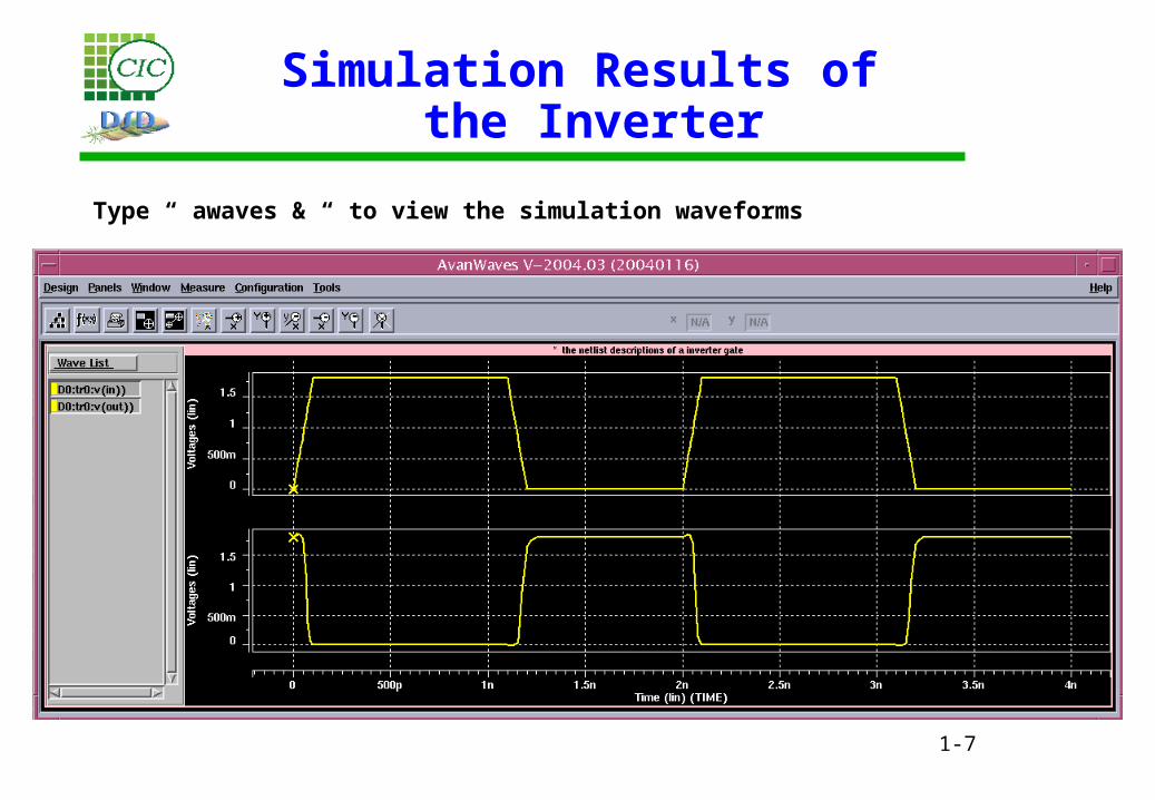
1-7
Simulation Results of the Inverter
Type “ awaves & “ to view the simulation waveforms
1-8
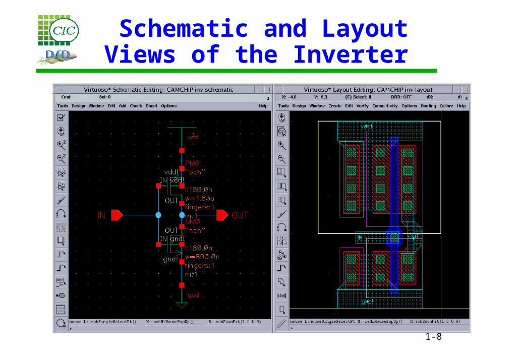
Schematic and Layout Views of the Inverter

1-9
A 2-Input NAND Gate Circuit Design
* The file name : NAND2.sp
.lib ‘./rf018.l' TT
MP1 VDD A OUT VDD pch w=2u l=0.18uMP2 VDD B OUT VDD pch w=2u l=0.18u MN1 NET1 A OUT GND nch w=2u l=0.18u MN2 GND B NET1 GND nch w=2u l=0.18u
VDD VDD 0 DC 1.8VVA A 0 pulse(0V 1.8V 0n 0.1n 0.1n 1n 2n)VB B 0 pulse(0V 1.8V 0n 0.1n 0.1n 2n 4n)
.OP
.TRAN 0.1n 4n
.OPTIONS POST
.END
VDD
GND
A
OUT
B
MP1 MP2
MN2
MN1
NET1
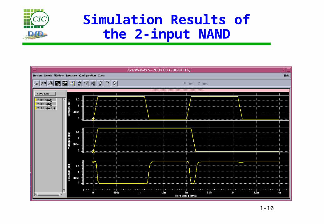
1-10
Simulation Results ofthe 2-input NAND
1-11
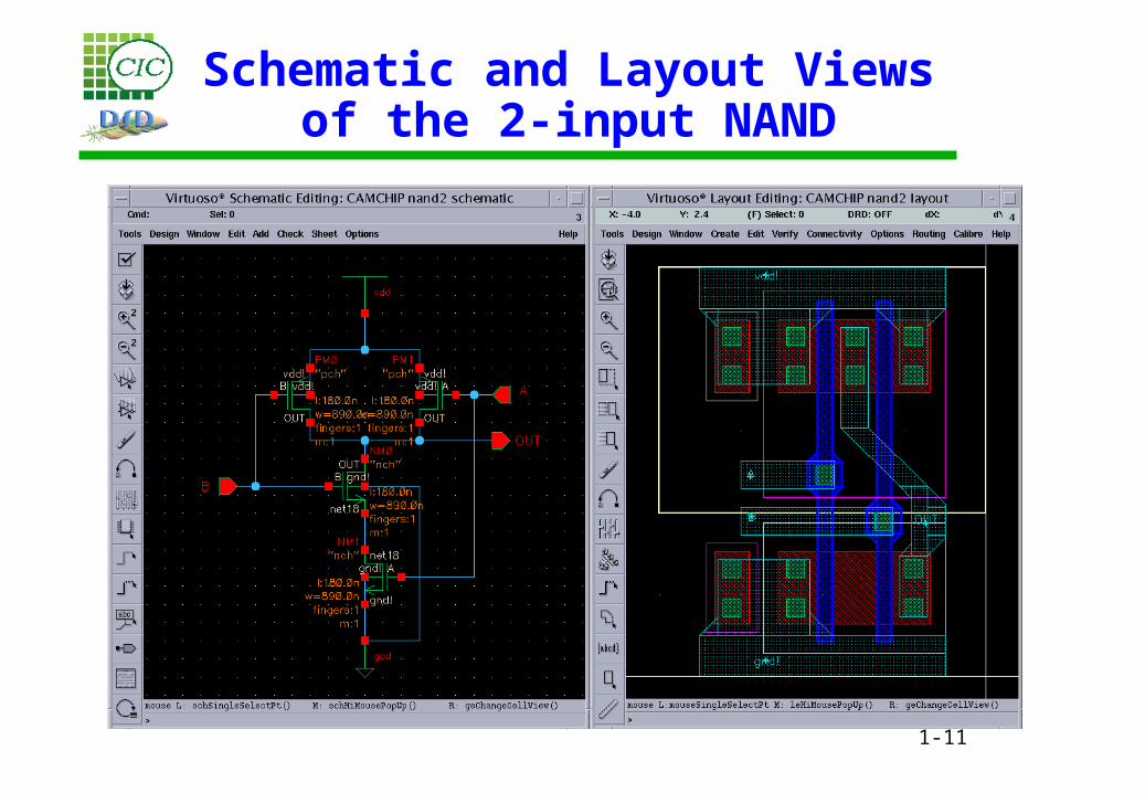
Schematic and Layout Views of the 2-input NAND
1-12
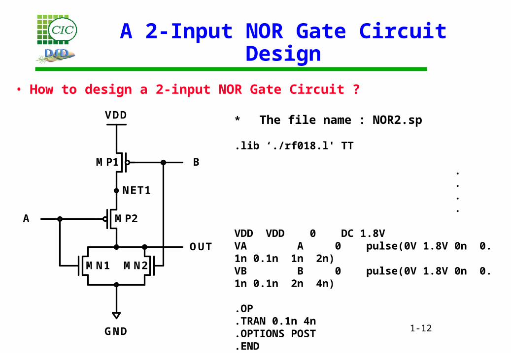
A 2-Input NOR Gate Circuit Design
• How to design a 2-input NOR Gate Circuit ?
* The file name : NOR2.sp
.lib ‘./rf018.l' TT
. . . .
VDD VDD 0 DC 1.8VVA A 0 pulse(0V 1.8V 0n 0.1n 0.1n 1n 2n)VB B 0 pulse(0V 1.8V 0n 0.1n 0.1n 2n 4n)
.OP
.TRAN 0.1n 4n
.OPTIONS POST
.END
VDD
GND
OUT
B
MN1 MN2
MP1
MP2
NET1
A
1-13
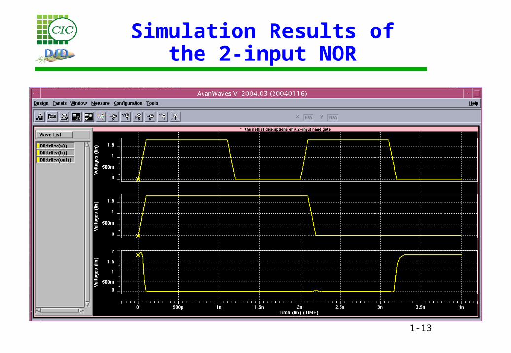
Simulation Results ofthe 2-input NOR
1-14
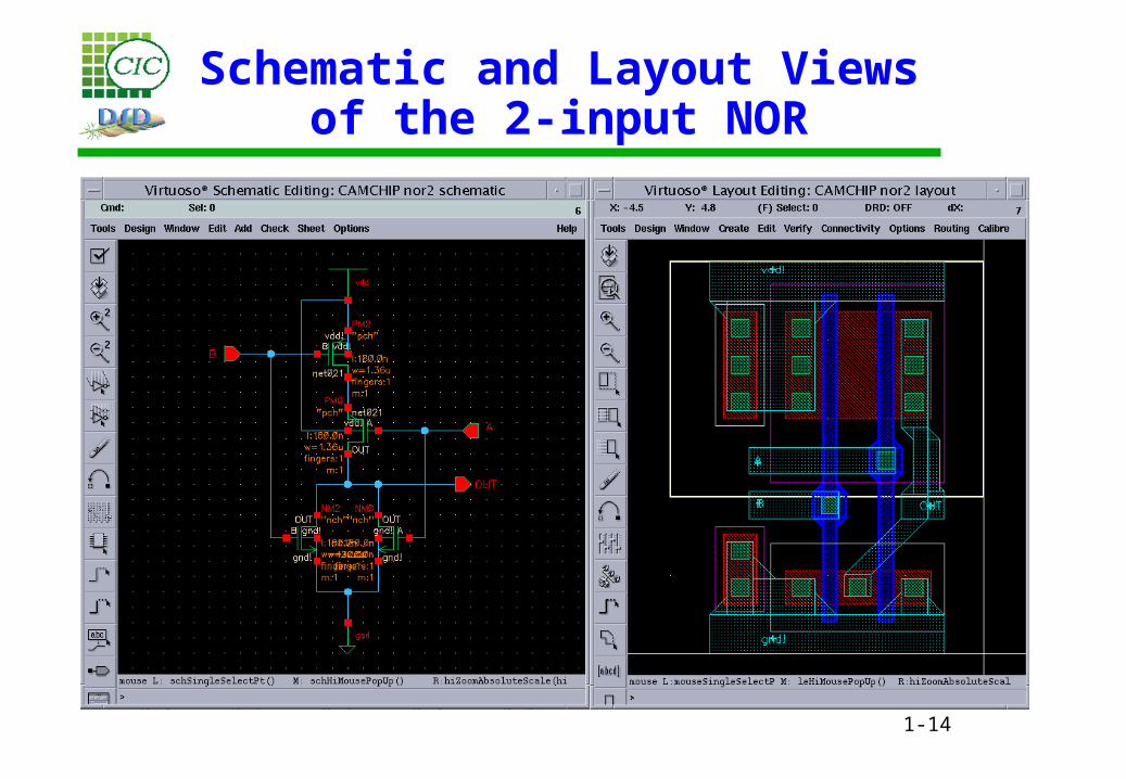
Schematic and Layout Views of the 2-input NOR
1-15
Lab
• A 3-input NAND Gate Circuit Design
• A 3-input NOR Gate Circuit Design
CBAOUT
CBAOUT

1-16
A layout diagram of Memory Circuit
1
9
1026
27
43
44 60
68
61
13:1
1-17
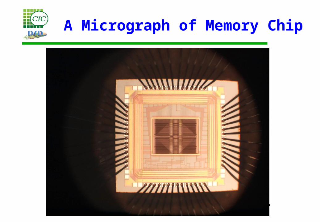
A Micrograph of Memory Chip