19 all-optical digital processing through semiconductor
TRANSCRIPT
All-optical digital processing through semiconductor optical amplifiers: state
of the art and perspectives
Gianluca Berrettini2, Antonella Bogoni1, Emma Lazzeri2, Gianluca Meloni2, Claudio Porzi2, Luca Potì1
and Mirco Scaffardi1 1Consorzio Nazionale Interuniversitario per le Telecomunicazioni (CNIT), Pisa
2Scuola Superiore Sant’Anna, Pisa 1Italy 2Italy
1. Introduction
Photonic digital processing is a capability which interest has been growing in for a long time. The main advantage of the photonic processing with respect to the electronic processing is the high speed (Tangdiongga et al., 2007; Liu et al., 2007). Nevertheless photonics is in its early stage and the realisation of complete all-optical computing system is still far, mainly due to the lack of efficient all optical memories. Despite the present limitations, photonic digital processing shows promise in the applications where fast computation speed is required. One of these scenarios is represented by the all-optical short-range photonic interconnection networks. The improvement of the present high performance computing systems is hampered by the bottleneck of the chip-to-chip and chip-to-memory communication. The limit is represented by the wiring density, the high power consumption and the throughput (Shacham et al., 2005). Photonic interconnection networks can overcome the limitations of the electronic interconnection networks by guaranteeing high bit rate communications, data format transparency and electromagnetic field immunity. Moreover they can reduce the wiring density and the power consumption. In such networks photonic digital processing can be the most suitable paradigm for simple and ultra-fast control and switching operations, since it reduces the packet latency to the optical time-of-flight. Elementary logic gates as AND, NOR, NAND, NOT, XOR are the basic functions necessary to realizing digital processing. Nevertheless for the controlling of all-optical interconnection networks several complex functions are required. Among them, two important functions are the managing of the contentions and the controlling of the switch. Moreover for a more flexible and effective managing of the network the priority information has to be carried by the packet label. In case of packets directed to the same node output port, the priority field of the contending packet is compared. The packet with the highest priority is directed to the
19
www.intechopen.com
Semiconductor Technologies438
designated output port. The other packet is delayed or discharged. Therefore a complex photonic digital circuit, able to compare two boolean numbers, is mandatory (Andriolli et al., 2007). All-optical subsystems able to discriminate if an N-bit (with N1) pattern representing a boolean number is greater or lower than another one are not reported yet. Calculating the addition of boolean numbers is another important functionality to perform packet header processing. If some packets are routed to the wrong link or are mislabelled, they can be routed in circles without reaching the destination. These loops are a cause of network congestion and must be avoided. A Time-To-Live (TTL) field in the packet prevents the formation of loops. This field represents the maximum number of hops of a packet and it is decremented after each node. When the field value is zero, the packet is discharged (McGeehan et al., 2003). The implementation of this functionality requires an all-optical processing circuit able to perform the decrementing of the boolean number in the TTL field. This operation can be performed by means of an all optical full-adder applying the so called method of complements (Hayes 1998). Moreover the all-optical full-adder can find application in resolving the Viterbi algorithm in the Maximum-Likelihood Sequence Estimation (MLSE) (Forney 1973; Proakis 1996). This method requires performing fast additions. An all-optical implementation of this algorithm can improve its efficiency. Other two important functions are analog-to-digital conversion (ADC) and digital-to-analog conversion (DAC). ADC is a key functionality which, converting continuous-time signals to digital binary signals, enables them to be transmitted through the modern digital communication networks. Applications regard e.g. radar signals, high-definition video, real-time signal monitoring, ultra-fast dispersion compensation. Although it didn’t receive the same attention as all-optical analog-to-digital conversion, DAC and/or multilevel codification in the optical domain has also been extensively investigated in order to implement some ultra-fast signal processing functions. These functions include, for instance, pattern recognition for header extraction (Saida et al., 2001), amplitude multiplexing for increasing spectral efficiency (Abbade et al., 2005) or label/payload encoding techniques (Abbade et al., 2006), and waveform generation for radar and display applications (Yacoubian & Das, 2003). The photonic digital processing is effective and attractive if it can be realised with integrated solutions. SOAs have shown to be attractive because of their compactness, stability, low switching energy and low latency. SOAs are reliable, relatively low cost devices which can be integrated within complex optical circuits with hybrid techniques (Maxwell, 2008; Lal et al., 2007; Kehayas et al., 2006 b). In this perspective, the possibility of using a single basic building gate for implementing all the complex logic functions is practical. In this chapter new schemes for the implementation of SOA-based reconfigurable logic gates, a photonic combinatorial network, a comparator, a full-adder, a digital-to–analog converter and an analog-to-digital converter will be presented.
2. Reconfigurable logic gates with a single SOA
Scheme of all-optical logic gates are reported in literature, using nonlinear effects in optical fibers (Bogoni et al., 2005; Chbat et al., 1992), in semiconductor devices (Ibrahim et al., 2003; Dorren et al., 2004) or in waveguides (Collecutt & Drummond, 2000). Moreover several efforts have been done to demonstrate the suitability of new structures for the realization of optical logic gates (Wu, 2005; Brzozowski & Sargent, 2001). In particular SOAs are very
www.intechopen.com
All-optical digital processing through semiconductor optical ampliiers: state of the art and perspectives 439
attractive nonlinear elements for the realization of different logic functions, due to their strong change of the refractive index together with high gain. Moreover, differently from fiber devices, SOAs allow photonic integration. In some schemes, SOA-based logic gates require interferometric structures including two or more devices with identical characteristics (Dorren et al., 2004) that need accurate control and stabilization. A practical and efficient solution makes use of a single SOA to realize the XNOR logic function, by exploiting simultaneously Four Wave Mixing (FWM) and Cross Gain Modulation (XGM) (Kumar & Willner, 2004; Berrettini et al., 2006 a). This architecture avoids using tricky interferometric configurations. Moreover it is easily reconfigurable: the same architecture can also implement NOT, AND, and NOR logic gates, merely turning on or off a probe signal. The use of a counter-propagating Continuous Wave (CW) light reduces the SOA response times, by increasing the maximum bit rate of the signals to be processed. In more details, the presence of the CW light allows to increase the mean saturation level of the SOA, thus reducing the dynamics of the gain recovery after the arrival of the input signals. In this way the signal distortions due to the SOA pattern effects can be minimized, thus allowing to process ultra-fast signals. All the new aspects of this scheme contribute to strongly reduce the complexity and the instability of the implementation, realizing an ultra-fast and reconfigurable logic gate.
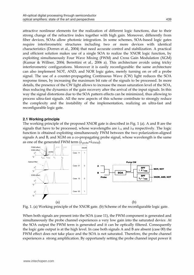
2.1 Working principle The working principle of the proposed XNOR gate is described in Fig. 1 (a). A and B are the signals that have to be processed, whose wavelengths are A and B respectively. The logic function is obtained exploiting simultaneously FWM between the two polarization-aligned signals A and B, and XGM on a co-propagating probe signal, whose wavelength is the same as one of the generated FWM term (probe=FWM).
XGM effect
FWM effectXGM effect
A Bprobe FWM
Case 11
Case 01
Case 10
Case 00
XNOR
0
0
1
1
Optical filter
ch Bch A
probe
x
y
x
y
x
y
x
y
XNOR, AND, NOT
SOABPF2 = FWM
BPF ≠ FWM
Pump CW
NOR, NOTA
B
Probe XNOR, AND, NOT
SOABPF2 = FWM
BPF ≠ FWM
Pump CW
NOR, NOTA
B
Probe
(a) (b) Fig. 1. (a) Working principle of the XNOR gate. (b) Scheme of the reconfigurable logic gate. When both signals are present into the SOA (case 11), the FWM component is generated and simultaneously the probe channel experiences a very low gain into the saturated device. At the SOA output the FWM term is generated and it can be optically filtered. Consequently the logic gate output is at the high level. In case both signals A and B are absent (case 00) the FWM effect does not take place and the SOA is not saturated. Therefore, the probe channel experiences a strong amplification. By opportunely setting the probe channel input power it
www.intechopen.com
Semiconductor Technologies440
is possible to equalize the high power level at the gate output in the case 00, which is equal to FWM component in the case 11. On the other hand, if only one of the signals A and B is present (cases 10 and 01) the FWM does not occur but the SOA is saturated, strongly reducing the gain of the probe. In these cases at the output the power level is low. In Fig. 1 (b) it is shown the scheme of the reconfigurable SOA-based logic gate. The proposed scheme can be exploited not only to realize the XNOR logic gate, but also AND, NOR and NOT functionalities, maintaining the same input conditions for the signals A and B. In particular, if the probe channel is turned off, the output of the optical filter centered at FWM represents a FWM-based logic function AND. Moreover, by changing the wavelength of the probe channel so that probe≠FWM allows to extract the NOR signal, using an optical band pass filter centered at probe. In this case, the NOR gate is based on XGM in the SOA. Finally, the NOT function can be obtained considering only one input signal in both gate output, by exploiting XGM on the probe channel. Therefore the simple and integrable scheme reported in Fig. 1 (b), which includes two different filters at the output of the SOA, can be easily reconfigured to obtain different logic gates, just controlling the wavelength of the probe channel or turning it off. The proposed scheme is suitable for both Non Return-to-Zero (NRZ) or Return-to-Zero (RZ) signals. In order to avoid the phase interference between probe and FWM component, the probe channel is launched into the SOA with orthogonal polarization with respect to the signals and consequently to the FWM term. The pulsed signals A and B have the same input peak power, and it is high enough to saturate the device and to induce a high-efficiency FWM effect. The probe peak power is sufficiently low to avoid SOA saturation. To eliminate pattern dependent signal distortions, a counter-propagating high-power CW light has been launched into the device, decreasing the mean life time of the carriers and keeping an optimum saturation level in the SOA.
2.2 Performance of the logic gate
Time [100 ps/Div]
Phot
orec
eive
d am
plitu
de
[a.u
.]
T ime [20 ps/Div]
Phot
orec
eive
d am
plitu
de
[a.u
.]
Oscilloscope Trace Eye Diagram
Ch A
Ch B
AND
NOR
NOT A
XNOR
Ch A
Ch B
AND
NOR
NOT A
XNOR
-11 -10 -9 -8 -7 -6 -5 -41E-12
1E-10
1E-8
1E-6
1E-4
0,01
1
BER
Received peak power [dBm]
BtoB chABtoB chBANDXNORNOTNOR
-11 -10 -9 -8 -7 -6 -5 -41E-12
1E-10
1E-8
1E-6
1E-4
0,01
1
-11 -10 -9 -8 -7 -6 -5 -41E-12
1E-10
1E-8
1E-6
1E-4
0,01
1
BER
Received peak power [dBm]
BtoB chABtoB chBANDXNORNOTNOR
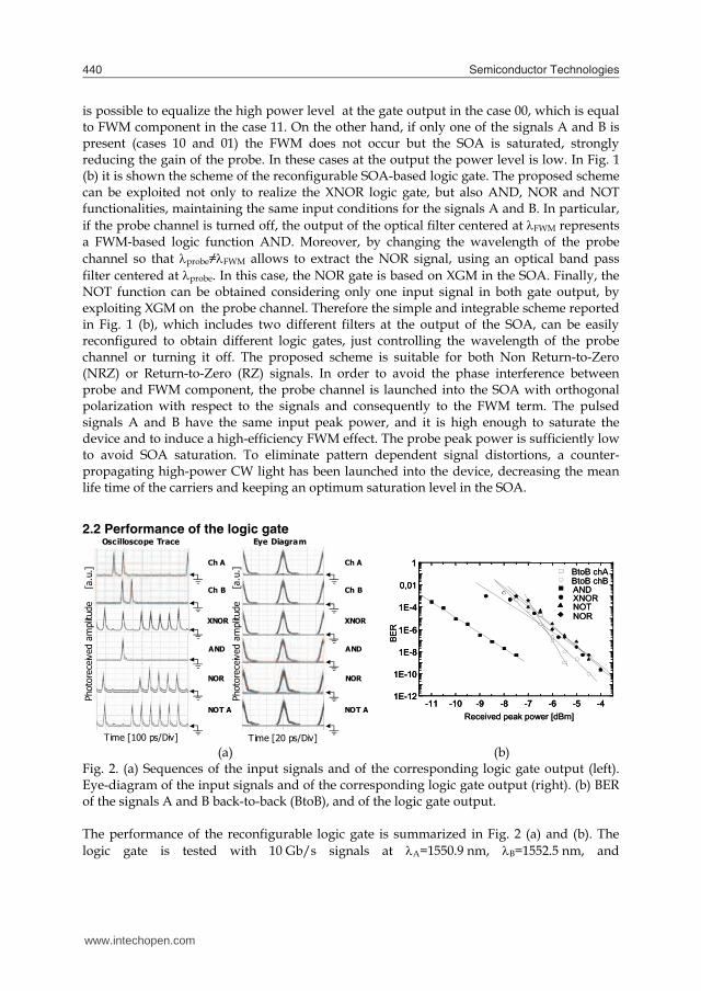
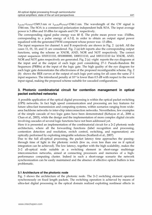
(a) (b) Fig. 2. (a) Sequences of the input signals and of the corresponding logic gate output (left). Eye-diagram of the input signals and of the corresponding logic gate output (right). (b) BER of the signals A and B back-to-back (BtoB), and of the logic gate output. The performance of the reconfigurable logic gate is summarized in Fig. 2 (a) and (b). The logic gate is tested with 10 Gb/s signals at A=1550.9 nm, B=1552.5 nm, and
www.intechopen.com
All-optical digital processing through semiconductor optical ampliiers: state of the art and perspectives 441
probe=FWM=1549.3 nm or probe≠FWM=1546.1 nm. The wavelength of the CW signal is 1544 nm. The SOA is a commercial polarization independent bulk SOA. The input average power is 3 dBm and 10 dBm for signals and CW respectively. The corresponding signal pulse energy was 40 fJ. The probe mean power was -15dBm, corresponding to a pulse energy of 6.3 fJ, in order to obtain an output signal power equalized with the generated FWM component whose power was -13 dBm. The input sequences for channel A and B respectively are shown in Fig. 2 (a)-left. All the cases 11, 01, 10, and 11 are considered. Fig. 2 (a)-left reports also the corresponding output functions, using the scheme as XNOR, AND, NOR and NOT respectively. The correct output sequences 1010111110, 0010000000, 1000111110, and 1001111110 for XNOR, AND, NOR and NOT gates respectively are generated. Fig. 2 (a) –right reports the eye diagrams at the input and at the output of each logic port considering 231-1 Pseudo-Random Bit Sequences (PRBSs) at the input of the logic gate. The high quality of the eye diagram for each logic gate demonstrates the effectiveness of the proposed reconfigurable scheme. Fig. 2 (b) shows the BER curves at the output of each logic port using for all cases the same 27-1 input sequence. The introduced penalty at 10-9 is lower than 0.5 dB with respect to the worst input signal, making the proposed scheme suitable for cascaded configurations.
3. Photonic combinatorial circuit for contention management in optical packet switched networks
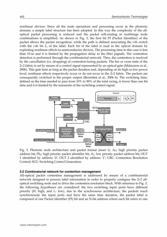
A possible application of the optical digital processing is within the optical packet switching (OPS) networks. In fact high speed communication and processing are key features for future ultra-fast transmission and computing systems, within scenarios ranging from wide-area backbone networks to inter-chip interconnection networks. Nevertheless, few examples of the simple cascade of two logic gates have been demonstrated (Kehayas et al., 2006 a; Chan et al., 2003), while the design and the implementation of more complex digital circuits involving cascades of several logic functions have not been addressed yet. Here it is presented an implementation of the combinatorial circuit for a 22 photonic node architecture, where all the forwarding functions (label recognition and processing, contention detection and resolution, switch control, switching, and regeneration) are optically performed by exploiting integrable solutions (Scaffardi et al., 2007). Due to the full all-optical processing, the packet latency time approaches the passing-through time of light in the photonic switch (few ns, even less than one ns if optical integration can be achieved). The low latency, together with the high scalability, makes the 22 all-optical node suitable as a switching element in short-range multistage interconnection networks, aimed at connecting processors and memories of a high-performance computing cluster. Indeed in such a short-range scenario the network synchronization can be easily maintained and the absence of effective optical buffers is less problematic. 3.1 Architecture of the photonic node Fig. 3 shows the architecture of the photonic node. The 22 switching element operates synchronously on fixed length packets. The switching operation is achieved by means of ultra-fast digital processing in the optical domain realized exploiting nonlinear effects in
www.intechopen.com
Semiconductor Technologies442
nonlinear devices. Since all the node operations and processing occur in the photonic domain, a simple label structure has been adopted. In this way the complexity of the all-optical packet processing is reduced and the packet self-routing in multistage node combinations is simplified. As shown in Fig. 3, the first bit PI (Packet Identifier) of the packet allows the packet recognition, while the path is defined associating the i-th switch with the i-th bit Li of the label. Each bit of the label is read in the optical domain by exploiting nonlinear effects in semiconductor devices. The processing time in this case is less than 10 ns and it is limited by the propagation delay in the fiber pigtails. The contention detection is performed through the combinatorial network. Then, the contention is resolved by the cancellation (i.e. dropping) of contention-losing packets. The bar or cross state of the 22 fabric is set by means of a control signal represented by an optical gate (Malacarne et al., 2006). This gate lasts as long as the packet duration and, depending on its high or low power level, nonlinear effects respectively occur or do not occur in the 22 fabric. The packets are consequently switched to the proper output (Berrettini et al., 2006 b). The switching time, defined as the time needed to pass from 10% to 90% of the total swing, is lower than one bit time and it is limited by the transients of the switching control signal.
Output 2 ContentionResolution
(packetcancellation)
LabelExtractor
Low priority input INL
High priority input INH
In L
In H
Out 2
Out 1
2x2 Optical Fabric
Opticaldelay
Opticaldelay
CRC
Output 1
PacketRecognizer
LabelExtractor
Contention Management
Optical FabricController
PPayload An A2 A1 PI
PPacket
SCG
PPIHH
AHH
AL
Fig. 3. Photonic node architecture and packet format (inset 1). AH: high priority packet address bit; PIH: high priority packet identifier bit; AL: low priority packet address bit; OUT 1 identified by address ‘0’; OUT 2 identified by address ‘1’; CRC: Contention Resolution Control; SCG: Switching Control Generation.
3.2 Combinatorial network for contention management All-optical packet contention management is addressed by means of a combinatorial network designed to process label information in order to properly configure the 22 all-optical switching node and to drive the contention resolution block. With reference to Fig. 3, the following hypotheses are considered: the two switching input ports have different priority (H: high, and L: low), due to the synchronous architecture, the packets reach synchronously the input ports and have the same time duration, the packet label is composed of one Packet Identifier (PI) bit and an N-bit address where each bit refers to one
www.intechopen.com
All-optical digital processing through semiconductor optical ampliiers: state of the art and perspectives 443
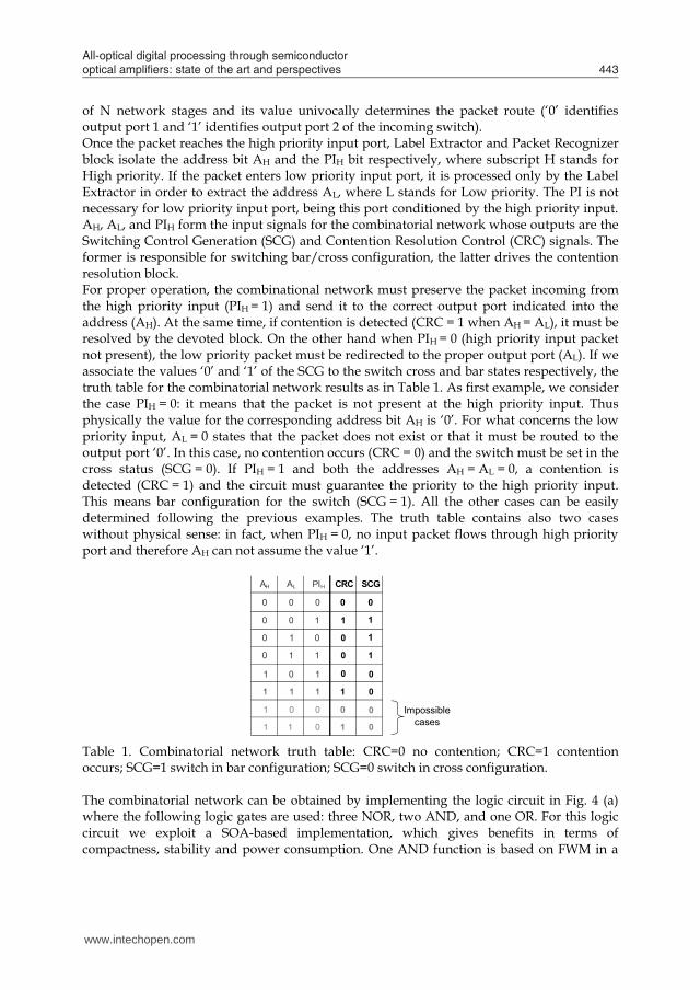
of N network stages and its value univocally determines the packet route (‘0’ identifies output port 1 and ‘1’ identifies output port 2 of the incoming switch). Once the packet reaches the high priority input port, Label Extractor and Packet Recognizer block isolate the address bit AH and the PIH bit respectively, where subscript H stands for High priority. If the packet enters low priority input port, it is processed only by the Label Extractor in order to extract the address AL, where L stands for Low priority. The PI is not necessary for low priority input port, being this port conditioned by the high priority input. AH, AL, and PIH form the input signals for the combinatorial network whose outputs are the Switching Control Generation (SCG) and Contention Resolution Control (CRC) signals. The former is responsible for switching bar/cross configuration, the latter drives the contention resolution block. For proper operation, the combinational network must preserve the packet incoming from the high priority input (PIH = 1) and send it to the correct output port indicated into the address (AH). At the same time, if contention is detected (CRC = 1 when AH = AL), it must be resolved by the devoted block. On the other hand when PIH = 0 (high priority input packet not present), the low priority packet must be redirected to the proper output port (AL). If we associate the values ‘0’ and ‘1’ of the SCG to the switch cross and bar states respectively, the truth table for the combinatorial network results as in Table 1. As first example, we consider the case PIH = 0: it means that the packet is not present at the high priority input. Thus physically the value for the corresponding address bit AH is ‘0’. For what concerns the low priority input, AL = 0 states that the packet does not exist or that it must be routed to the output port ‘0’. In this case, no contention occurs (CRC = 0) and the switch must be set in the cross status (SCG = 0). If PIH = 1 and both the addresses AH = AL = 0, a contention is detected (CRC = 1) and the circuit must guarantee the priority to the high priority input. This means bar configuration for the switch (SCG = 1). All the other cases can be easily determined following the previous examples. The truth table contains also two cases without physical sense: in fact, when PIH = 0, no input packet flows through high priority port and therefore AH can not assume the value ‘1’.
PIHAH AL SCGCRC
0
1
0 0 0 0
0 1
1
0
1
1 0
0
0
0 0
0
1
1
1
1 1
1
1
1
1
0
1
1 1
0
0
10
0
0
0
0
0
Impossiblecases
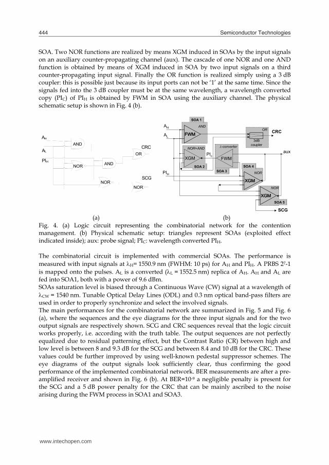
Table 1. Combinatorial network truth table: CRC=0 no contention; CRC=1 contention occurs; SCG=1 switch in bar configuration; SCG=0 switch in cross configuration. The combinatorial network can be obtained by implementing the logic circuit in Fig. 4 (a) where the following logic gates are used: three NOR, two AND, and one OR. For this logic circuit we exploit a SOA-based implementation, which gives benefits in terms of compactness, stability and power consumption. One AND function is based on FWM in a
www.intechopen.com
Semiconductor Technologies444
SOA. Two NOR functions are realized by means XGM induced in SOAs by the input signals on an auxiliary counter-propagating channel (aux). The cascade of one NOR and one AND function is obtained by means of XGM induced in SOA by two input signals on a third counter-propagating input signal. Finally the OR function is realized simply using a 3 dB coupler: this is possible just because its input ports can not be ‘1’ at the same time. Since the signals fed into the 3 dB coupler must be at the same wavelength, a wavelength converted copy (PIC) of PIH is obtained by FWM in SOA using the auxiliary channel. The physical schematic setup is shown in Fig. 4 (b).
AH
AL
PIH
CRC
SCG
AND
AND
OR
NORNOR
NOR
FWMFWM
XGM
XGMXGM
XGMXGM
PIcaux
3dBcoupler
SCG
CRC
PIH
AL
AH
FWM
ANDOR
NOR+AND
NOR
NOR
-converter
SOA 1
SOA 2 SOA 3
SOA 4
SOA 5
(a) (b)
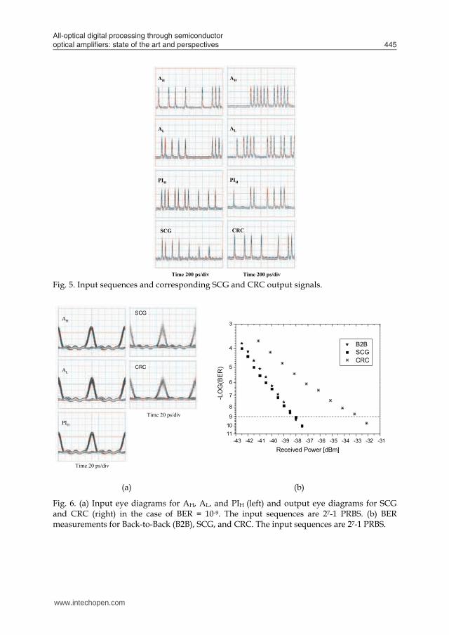
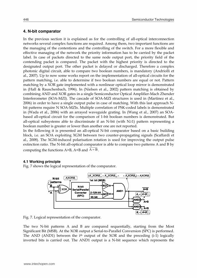
Fig. 4. (a) Logic circuit representing the combinatorial network for the contention management. (b) Physical schematic setup: triangles represent SOAs (exploited effect indicated inside); aux: probe signal; PIC: wavelength converted PIH. The combinatorial circuit is implemented with commercial SOAs. The performance is measured with input signals at H= 1550.9 nm (FWHM: 10 ps) for AH and PIH. A PRBS 27-1 is mapped onto the pulses. AL is a converted (L = 1552.5 nm) replica of AH. AH and AL are fed into SOA1, both with a power of 9.6 dBm. SOAs saturation level is biased through a Continuous Wave (CW) signal at a wavelength of CW = 1540 nm. Tunable Optical Delay Lines (ODL) and 0.3 nm optical band-pass filters are used in order to properly synchronize and select the involved signals. The main performances for the combinatorial network are summarized in Fig. 5 and Fig. 6 (a), where the sequences and the eye diagrams for the three input signals and for the two output signals are respectively shown. SCG and CRC sequences reveal that the logic circuit works properly, i.e. according with the truth table. The output sequences are not perfectly equalized due to residual patterning effect, but the Contrast Ratio (CR) between high and low level is between 8 and 9.3 dB for the SCG and between 8.4 and 10 dB for the CRC. These values could be further improved by using well-known pedestal suppressor schemes. The eye diagrams of the output signals look sufficiently clear, thus confirming the good performance of the implemented combinatorial network. BER measurements are after a pre-amplified receiver and shown in Fig. 6 (b). At BER=10-9 a negligible penalty is present for the SCG and a 5 dB power penalty for the CRC that can be mainly ascribed to the noise arising during the FWM process in SOA1 and SOA3.
www.intechopen.com
All-optical digital processing through semiconductor optical ampliiers: state of the art and perspectives 445
Time 200 ps/div
AH
AL
PIH
SCG
Time 200 ps/div
AH
AL
PIH
CRC
Fig. 5. Input sequences and corresponding SCG and CRC output signals.
Time 20 ps/div
AH
AL
PIH
CRC
SCG
Time 20 ps/div
-43 -42 -41 -40 -39 -38 -37 -36 -35 -34 -33 -32 -3111109
8
7
6
5
4
3
-LO
G(B
ER
)
Received Power [dBm]
B2B SCG CRC
(a) (b)
Fig. 6. (a) Input eye diagrams for AH, AL, and PIH (left) and output eye diagrams for SCG and CRC (right) in the case of BER = 10-9. The input sequences are 27-1 PRBS. (b) BER measurements for Back-to-Back (B2B), SCG, and CRC. The input sequences are 27-1 PRBS.
www.intechopen.com
Semiconductor Technologies446
4. N-bit comparator
In the previous section it is explained as for the controlling of all-optical interconnection networks several complex functions are required. Among them, two important functions are the managing of the contentions and the controlling of the switch. For a more flexible and effective managing of the network the priority information has to be carried by the packet label. In case of packets directed to the same node output port, the priority field of the contending packet is compared. The packet with the highest priority is directed to the designated output port. The other packet is delayed or discharged. Therefore a complex photonic digital circuit, able to compare two boolean numbers, is mandatory (Andriolli et al., 2007). Up to now some works report on the implementation of all-optical circuits for the pattern matching, i.e. able to determine if two boolean numbers are equal or not. Pattern matching by a XOR gate implemented with a nonlinear optical loop mirror is demonstrated in (Hall & Rauschenbach, 1996). In (Nielsen et al., 2002) pattern matching is obtained by combining AND and XOR gates in a single Semiconductor Optical Amplifier-Mach Zhender Interferometer (SOA-MZI). The cascade of SOA-MZI structures is used in (Martinez et al., 2006) in order to have a single output pulse in case of matching. With this last approach N-bit patterns require N SOA-MZIs. Multiple correlation of PSK-coded labels is demonstrated in (Wada et al., 2006) with an arrayed waveguide grating. In (Wang et al., 2007) an SOA-based all-optical circuit for the comparison of 1-bit boolean numbers is demonstrated. But all-optical subsystems able to discriminate if an N-bit (with N1) pattern representing a boolean number is greater or lower than another one are not reported. In the following it is presented an all-optical N-bit comparator based on a basic building block, i.e. an SOA exploiting XGM between two counter-propagating signals (Scaffardi et al., 2008). The XGM-induced polarisation rotation is used for improving the output pulse extinction ratio. The N-bit all-optical comparator is able to compare two patterns A and B by computing the functions A>B, A<B and BA .
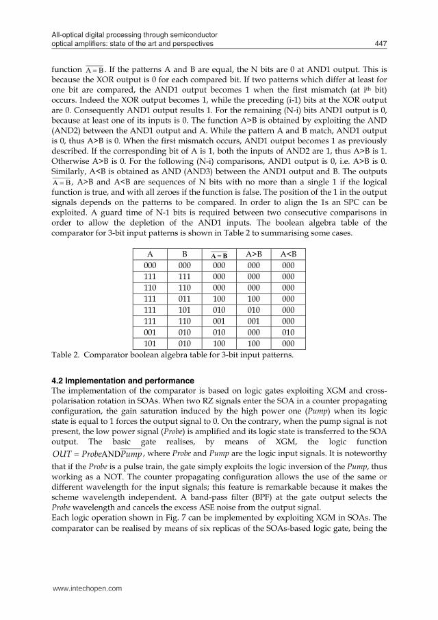
4.1 Working principle Fig. 7 shows the logical representation of the comparator.
XORA
B N-bitSerial/Parallel
Converter(SPC)
1st bit (MSB)
ith bit
NOT
AND1
AND2
AND3
A>B
A<B
NOT(i-1)th bitA=B
N-bitpatterns
(Ai-1XORBi-1 Ai-2XORBi-2 A0XORB0) AiXORBiAiXORBi
Ai A=B i
Bi A=B i
XORA
B N-bitSerial/Parallel
Converter(SPC)
1st bit (MSB)
ith bit
NOT
AND1
AND2
AND3
A>B
A<B
NOT(i-1)th bitA=B
N-bitpatterns
(Ai-1XORBi-1 Ai-2XORBi-2 A0XORB0) AiXORBiAiXORBi
Ai A=B iAi A=B i
Bi A=B iBi A=B i Fig. 7. Logical representation of the comparator. The two N-bit patterns A and B are compared sequentially, starting from the Most Significant Bit (MSB). At the XOR output a Serial-to-Parallel Conversion (SPC) is performed. The AND (AND1) between the ith output of the XOR and the preceding (i-1) logically inverted bits is carried out. The AND1 output is a N-bit sequence which represents the
www.intechopen.com
All-optical digital processing through semiconductor optical ampliiers: state of the art and perspectives 447
function BA . If the patterns A and B are equal, the N bits are 0 at AND1 output. This is because the XOR output is 0 for each compared bit. If two patterns which differ at least for one bit are compared, the AND1 output becomes 1 when the first mismatch (at ith bit) occurs. Indeed the XOR output becomes 1, while the preceding (i-1) bits at the XOR output are 0. Consequently AND1 output results 1. For the remaining (N-i) bits AND1 output is 0, because at least one of its inputs is 0. The function A>B is obtained by exploiting the AND (AND2) between the AND1 output and A. While the pattern A and B match, AND1 output is 0, thus A>B is 0. When the first mismatch occurs, AND1 output becomes 1 as previously described. If the corresponding bit of A is 1, both the inputs of AND2 are 1, thus A>B is 1. Otherwise A>B is 0. For the following (N-i) comparisons, AND1 output is 0, i.e. A>B is 0. Similarly, A<B is obtained as AND (AND3) between the AND1 output and B. The outputs
BA , A>B and A<B are sequences of N bits with no more than a single 1 if the logical function is true, and with all zeroes if the function is false. The position of the 1 in the output signals depends on the patterns to be compared. In order to align the 1s an SPC can be exploited. A guard time of N-1 bits is required between two consecutive comparisons in order to allow the depletion of the AND1 inputs. The boolean algebra table of the comparator for 3-bit input patterns is shown in Table 2 to summarising some cases.
A B BA A>B A<B
000 000 000 000 000 111 111 000 000 000 110 110 000 000 000 111 011 100 100 000 111 101 010 010 000 111 110 001 001 000 001 010 010 000 010 101 010 100 100 000
Table 2. Comparator boolean algebra table for 3-bit input patterns.
4.2 Implementation and performance The implementation of the comparator is based on logic gates exploiting XGM and cross-polarisation rotation in SOAs. When two RZ signals enter the SOA in a counter propagating configuration, the gain saturation induced by the high power one (Pump) when its logic state is equal to 1 forces the output signal to 0. On the contrary, when the pump signal is not present, the low power signal (Probe) is amplified and its logic state is transferred to the SOA output. The basic gate realises, by means of XGM, the logic function
PumpProbeOUT AND , where Probe and Pump are the logic input signals. It is noteworthy that if the Probe is a pulse train, the gate simply exploits the logic inversion of the Pump, thus working as a NOT. The counter propagating configuration allows the use of the same or different wavelength for the input signals; this feature is remarkable because it makes the scheme wavelength independent. A band-pass filter (BPF) at the gate output selects the Probe wavelength and cancels the excess ASE noise from the output signal. Each logic operation shown in Fig. 7 can be implemented by exploiting XGM in SOAs. The comparator can be realised by means of six replicas of the SOAs-based logic gate, being the
www.intechopen.com
Semiconductor Technologies448
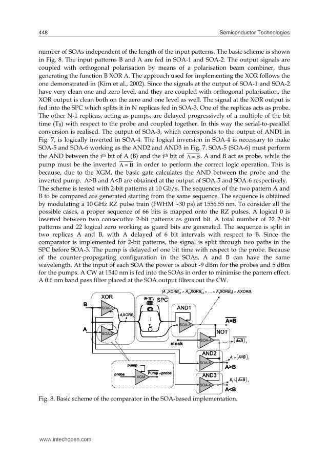
number of SOAs independent of the length of the input patterns. The basic scheme is shown in Fig. 8. The input patterns B and A are fed in SOA-1 and SOA-2. The output signals are coupled with orthogonal polarisation by means of a polarisation beam combiner, thus generating the function B XOR A. The approach used for implementing the XOR follows the one demonstrated in (Kim et al., 2002). Since the signals at the output of SOA-1 and SOA-2 have very clean one and zero level, and they are coupled with orthogonal polarisation, the XOR output is clean both on the zero and one level as well. The signal at the XOR output is fed into the SPC which splits it in N replicas fed in SOA-3. One of the replicas acts as probe. The other N-1 replicas, acting as pumps, are delayed progressively of a multiple of the bit time (TB) with respect to the probe and coupled together. In this way the serial-to-parallel conversion is realised. The output of SOA-3, which corresponds to the output of AND1 in Fig. 7, is logically inverted in SOA-4. The logical inversion in SOA-4 is necessary to make SOA-5 and SOA-6 working as the AND2 and AND3 in Fig. 7. SOA-5 (SOA-6) must perform the AND between the ith bit of A (B) and the ith bit of BA . A and B act as probe, while the pump must be the inverted BA in order to perform the correct logic operation. This is because, due to the XGM, the basic gate calculates the AND between the probe and the inverted pump. A>B and A<B are obtained at the output of SOA-5 and SOA-6 respectively. The scheme is tested with 2-bit patterns at 10 Gb/s. The sequences of the two pattern A and B to be compared are generated starting from the same sequence. The sequence is obtained by modulating a 10 GHz RZ pulse train (FWHM 30 ps) at 1556.55 nm. To consider all the possible cases, a proper sequence of 66 bits is mapped onto the RZ pulses. A logical 0 is inserted between two consecutive 2-bit patterns as guard bit. A total number of 22 2-bit patterns and 22 logical zero working as guard bits are generated. The sequence is split in two replicas A and B, with A delayed of 6 bit intervals with respect to B. Since the comparator is implemented for 2-bit patterns, the signal is split through two paths in the SPC before SOA-3. The pump is delayed of one bit time with respect to the probe. Because of the counter-propagating configuration in the SOAs, A and B can have the same wavelength. At the input of each SOA the power is about -9 dBm for the probes and 5 dBm for the pumps. A CW at 1540 nm is fed into the SOAs in order to minimise the pattern effect. A 0.6 nm band pass filter placed at the SOA output filters out the CW.
SOA-1B
A
…
(N-1)Tb
Tb SOA-3
SOA-4
SOA-5
SOA-6
A=B
A<B
A>B
clock
SOA-2
Pump probeXGM
pump
probe
XOR SPCAND1
AND3
AND2
NOT
AiXORBi
A=B i
Ai A=B i
Bi A=B i
(A -1XORBi-1 Ai-2XORBi-2 … A0XORB0) AiXORBi
SOA-1B
A
…
(N-1)Tb
Tb SOA-3
SOA-4
SOA-5
SOA-6
A=B
A<B
A>B
clock
SOA-2
Pump probeXGM
pump
probe
XOR SPCAND1
AND3
AND2
NOT
AiXORBi
A=B iA=B i
Ai A=B i
Bi A=B i
(A -1XORBi-1 Ai-2XORBi-2 … A0XORB0) AiXORBi
Fig. 8. Basic scheme of the comparator in the SOA-based implementation.
www.intechopen.com
All-optical digital processing through semiconductor optical ampliiers: state of the art and perspectives 449
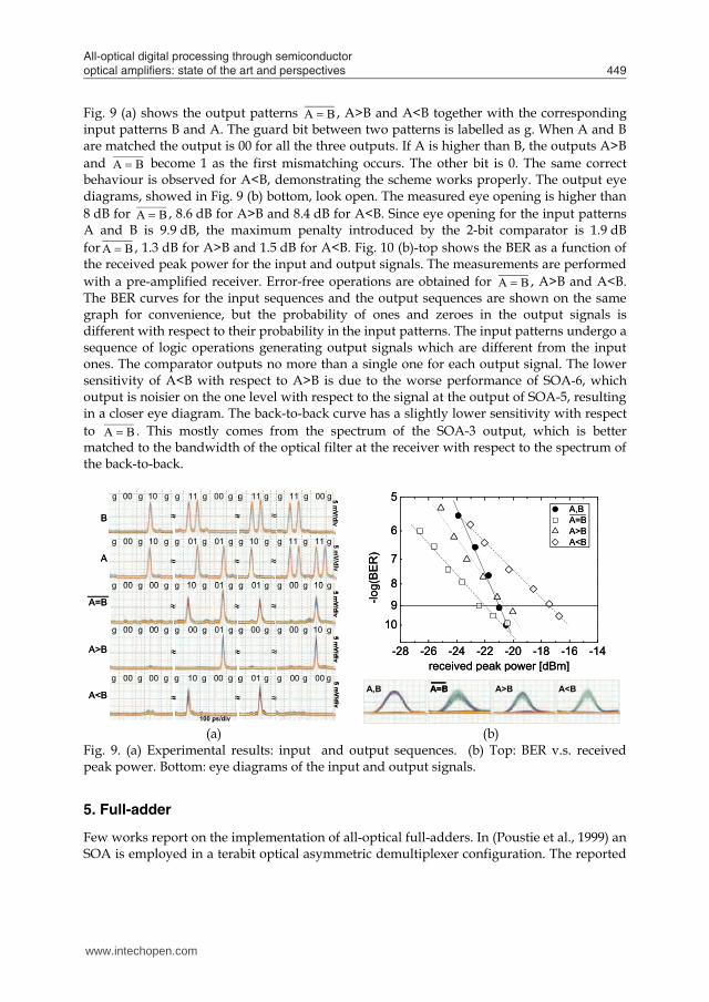
Fig. 9 (a) shows the output patterns BA , A>B and A<B together with the corresponding input patterns B and A. The guard bit between two patterns is labelled as g. When A and B are matched the output is 00 for all the three outputs. If A is higher than B, the outputs A>B and BA become 1 as the first mismatching occurs. The other bit is 0. The same correct behaviour is observed for A<B, demonstrating the scheme works properly. The output eye diagrams, showed in Fig. 9 (b) bottom, look open. The measured eye opening is higher than 8 dB for BA , 8.6 dB for A>B and 8.4 dB for A<B. Since eye opening for the input patterns A and B is 9.9 dB, the maximum penalty introduced by the 2-bit comparator is 1.9 dB for BA , 1.3 dB for A>B and 1.5 dB for A<B. Fig. 10 (b)-top shows the BER as a function of the received peak power for the input and output signals. The measurements are performed with a pre-amplified receiver. Error-free operations are obtained for BA , A>B and A<B. The BER curves for the input sequences and the output sequences are shown on the same graph for convenience, but the probability of ones and zeroes in the output signals is different with respect to their probability in the input patterns. The input patterns undergo a sequence of logic operations generating output signals which are different from the input ones. The comparator outputs no more than a single one for each output signal. The lower sensitivity of A<B with respect to A>B is due to the worse performance of SOA-6, which output is noisier on the one level with respect to the signal at the output of SOA-5, resulting in a closer eye diagram. The back-to-back curve has a slightly lower sensitivity with respect to BA . This mostly comes from the spectrum of the SOA-3 output, which is better matched to the bandwidth of the optical filter at the receiver with respect to the spectrum of the back-to-back.
A
B
A>B
A<B
A=B
100 ps/div
5 mV/div
5 mV/div
5 mV/div
5 mV/div
5 mV/div
g g g g g g g g g g g00 10 11 00 11 11 00
g g g g g g g g g g g00 10 01 01 10 11 11
g g g g g g g g g g g00 00 10 01 01 00 10
g g g g g g g g g g g00 00 00 01 00 00 10
g g g g g g g g g g g00 00 10 00 01 00 00
A
B
A>B
A<B
A=B
100 ps/div
5 mV/div
5 mV/div
5 mV/div
5 mV/div
5 mV/div
g g g g g g g g g g g00 10 11 00 11 11 00
g g g g g g g g g g g00 10 01 01 10 11 11
g g g g g g g g g g g00 00 10 01 01 00 10
g g g g g g g g g g g00 00 00 01 00 00 10
g g g g g g g g g g g00 00 10 00 01 00 00
-28 -26 -24 -22 -20 -18 -16 -14
10
9
8
7
6
5
-log(
BE
R)
received peak power [dBm]
A,B A=B A>B A<B
A,B A=B A>B A<B
-28 -26 -24 -22 -20 -18 -16 -14
10
9
8
7
6
5
-log(
BE
R)
received peak power [dBm]
A,B A=B A>B A<B
A,B A=BA=B A>B A<B
(a) (b)
Fig. 9. (a) Experimental results: input and output sequences. (b) Top: BER v.s. received peak power. Bottom: eye diagrams of the input and output signals.
5. Full-adder
Few works report on the implementation of all-optical full-adders. In (Poustie et al., 1999) an SOA is employed in a terabit optical asymmetric demultiplexer configuration. The reported
www.intechopen.com
Semiconductor Technologies450
operation speed is below 1 Gb/s. A faster full-adder is reported in (Kim et al., 2003) based on SOAs, but in that scheme the output sum depends directly on the carry in; moreover performances in terms of bit error-rate and eye opening are not reported. In the scheme presented in the following, both the sum and the output carry do not depend directly on the input carry. This helps improving the quality of the output signals in case of cascade of multiple full-adders.
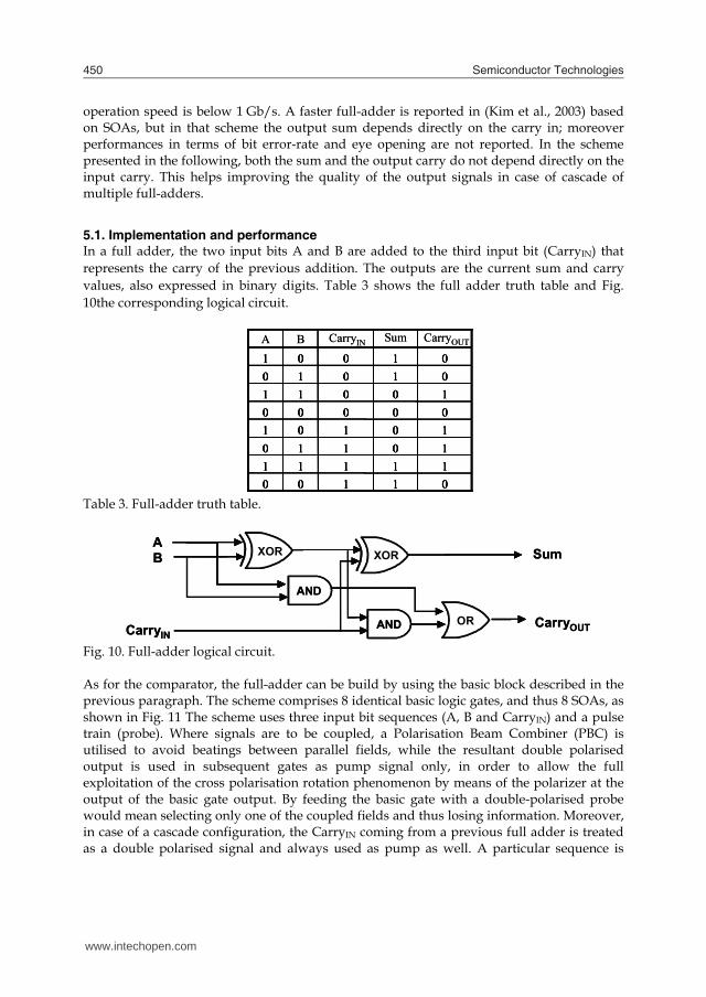
5.1. Implementation and performance In a full adder, the two input bits A and B are added to the third input bit (CarryIN) that represents the carry of the previous addition. The outputs are the current sum and carry values, also expressed in binary digits. Table 3 shows the full adder truth table and Fig. 10the corresponding logical circuit.
0110011111101101010100000100110101001001
SumCarryINBA
0110011111101101010100000100110101001001
CarryOUT
0110011111101101010100000100110101001001
SumCarryINBA
0110011111101101010100000100110101001001
CarryOUT
Table 3. Full-adder truth table.
XOR
AND
XOR
AND
AB Sum
CarryOUTCarryINOR
XOR
AND
XOR
AND
AB Sum
CarryOUTCarryINOR
Fig. 10. Full-adder logical circuit. As for the comparator, the full-adder can be build by using the basic block described in the previous paragraph. The scheme comprises 8 identical basic logic gates, and thus 8 SOAs, as shown in Fig. 11 The scheme uses three input bit sequences (A, B and CarryIN) and a pulse train (probe). Where signals are to be coupled, a Polarisation Beam Combiner (PBC) is utilised to avoid beatings between parallel fields, while the resultant double polarised output is used in subsequent gates as pump signal only, in order to allow the full exploitation of the cross polarisation rotation phenomenon by means of the polarizer at the output of the basic gate output. By feeding the basic gate with a double-polarised probe would mean selecting only one of the coupled fields and thus losing information. Moreover, in case of a cascade configuration, the CarryIN coming from a previous full adder is treated as a double polarised signal and always used as pump as well. A particular sequence is
www.intechopen.com
All-optical digital processing through semiconductor optical ampliiers: state of the art and perspectives 451
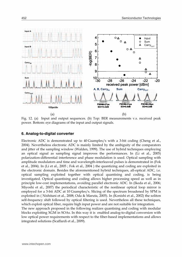
mapped onto the RZ pulse train with a Mach Zehnder Modulator (MZM). A, B and CarryIN are generating by splitting and opportunely delaying the pattern. In order to consider all the possible cases, a 24 bit sequence is produced and split in three replicas that are then delayed of 8 bit times with respect to each others. The signals have a repetition rate of 10 Gb/s at the wavelength of 1556.55 nm. The Band Pass Filters (BPF) in the setup have a bandwidth of 0.7 nm. To assess the scheme performances, the BER and the Eye Opening (EO) have been evaluated. The receiver used was a pre-amplified one comprising an EDFA, a tunable 0.25 nm bandwidth BPF used to optimise the received signal, and a 12.3 Gb/s photo-receiver. The traces of input and output sequences reported in Fig. 12(a) demonstrate the correct behaviour of the circuit. A limited pulse broadening can be noticed, mostly due to cascading filters with slightly different centre wavelength. The BER measurements, shown in Fig. 12(b) - top show error-free operations both on the Sum and CarryOUT signal. Fig. 12(b) - bottom shows the input and output eye diagrams. Open eyes are obtained for both the output sequences even if the Sum is less equalised than the CarryOUT output signal, and suffer from slow polarisation fluctuations.
PBCGATE 1
Fixed DelayFixed Delay
AB
EDFA
GATE 2
Fixed DelayB
A
GATE 3
Fixed DelayA
GATE 4
Fixed DelayFixed Delay
GATE 5
Fixed DelayProbe
GATE 6
Fixed Delay
GATE 7
Fixed DelayFixed Delay
GATE 8Carry IN Fixed Delay
Probe
PBC
PBCCarryOUT
OUT
EDFA
EDFA
EDFA
EDFAPBC
A AND B
B AND A
A XOR B
A AND (A XOR B)=A AND B
Carry IN
A XOR B
Carry IN AND (A XOR B)
A XOR B AND Carry IN
(A XOR B) XOR Carry IN
(A XOR B) OR Carry IN AND Carry IN
(A AND B) OR (Carry IN AND (A XOR B))
PBCPBCGATE 1
Fixed DelayFixed Delay
AB
EDFAEDFA
GATE 2
Fixed DelayB
A
GATE 3
Fixed DelayA
GATE 4
Fixed DelayFixed Delay
GATE 5
Fixed DelayProbe
GATE 6
Fixed Delay
GATE 7
Fixed DelayFixed Delay
GATE 8Carry IN Fixed Delay
Probe
PBCPBC
PBCPBCCarryOUT
OUT
EDFAEDFA
EDFAEDFA
EDFAEDFA
EDFAEDFAPBCPBC
A AND B
B AND A
A XOR B
A AND (A XOR B)=A AND B
Carry IN
A XOR B
Carry IN AND (A XOR B)
A XOR B AND Carry IN
(A XOR B) XOR Carry IN
(A XOR B) OR Carry IN AND Carry IN
(A AND B) OR (Carry IN AND (A XOR B))
Fig. 11. Full-adder implementation. These fluctuations are likely caused by mechanical stress on the fibres. The BER of the CarryOUT is measured in the best conditions, i.e. for the maximum eye opening. The eye closure penalty, measured in a long temporal scale, is 5.1 dB for the CarryOUT and 6.5 dB for the Sum. The polarisation stability of the system can be improved with an integrated implementation of the scheme.
www.intechopen.com
Semiconductor Technologies452
Fig. 12. (a) Input and output sequences. (b) Top: BER measurements v.s. received peak power. Bottom: eye diagrams of the input and output signals.
6. Analog-to-digital converter
Electronic ADC is demonstrated up to 40 Gsamples/s with a 3-bit coding (Cheng et al., 2004). Nevertheless electronic ADC is mainly limited by the ambiguity of the comparators and jitter of the sampling window (Walden, 1999). The use of hybrid techniques employing an optical signal as sampling signal improves the performances. In (Li et al., 2005) polarization-differential interference and phase modulation is used. Optical sampling with amplitude modulators and time and wavelength-interleaved pulses is demonstrated in (Fok et al., 2004). In (Li et al., 2005 ; Fok et al., 2004 ) the quantizing and coding are exploited in the electronic domain. Besides the aforementioned hybrid techniques, all-optical ADC, i.e. optical sampling exploited together with optical quantising and coding, is being investigated. Optical quantising and coding allows higher processing speed as well as in principle low-cost implementations, avoiding parallel electronic ADC. In (Ikeda et al., 2006; Miyoshi et al., 2007) the periodical characteristic of the nonlinear optical loop mirror is employed for a 3-bit ADC at 10 Gsamples/s. Slicing of the spectrum broadened by SPM is exploited in ( Nishitani et al., 2008; Oda & Maruta, 2005). In (Konishi et al., 2002) the soliton self-frequency shift followed by optical filtering is used. Nevertheless all these techniques, which exploit optical fiber, require high input power and are not suitable for integration. The new approach proposed in the following realizes quantising and coding with modular blocks exploiting XGM in SOAs. In this way it is enabled analog-to-digital conversion with low optical power requirements with respect to the fiber-based implementations and allows integrated solutions (Scaffardi et al., 2009).
Input A
Carry OUT
Sum
Carry IN
Input B
Input A
Carry OUT
Sum
Carry IN
Input B
Input A
Carry OUT
Sum
Carry IN
Input B
Input A
Carry OUT
Sum
Carry IN
Input B
100ps/div
Input A
Carry OUT
Sum
Carry IN
Input B
Input A
Carry OUT
Sum
Carry IN
Input B
Input A
Carry OUT
Sum
Carry IN
Input B
Input A
Carry OUT
Sum
Carry IN
Input B
100ps/div
-30 -28 -26 -24 -22 -2010
9
8
7
6
5
4 Input Sum Carry
OUT
-log(
BER
)received peak power [dBm]
FWHM=27psEO=13.3dB
A, B, CarryIN
FWHM=31psEO=6.8dB
Sum
FWHM=29psEO=8.2dB
CarryOUT
20ps/div 20ps/div 20ps/div
-30 -28 -26 -24 -22 -2010
9
8
7
6
5
4 Input Sum Carry
OUT
-log(
BER
)received peak power [dBm]
FWHM=27psEO=13.3dB
A, B, CarryIN
FWHM=31psEO=6.8dB
Sum
FWHM=29psEO=8.2dB
CarryOUT
20ps/div 20ps/div 20ps/div
(a) (b)
www.intechopen.com
All-optical digital processing through semiconductor optical ampliiers: state of the art and perspectives 453
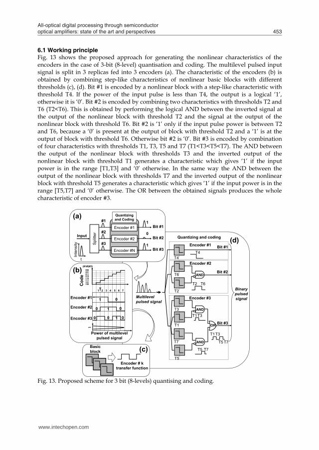
6.1 Working principle Fig. 13 shows the proposed approach for generating the nonlinear characteristics of the encoders in the case of 3-bit (8-level) quantisation and coding. The multilevel pulsed input signal is split in 3 replicas fed into 3 encoders (a). The characteristic of the encoders (b) is obtained by combining step-like characteristics of nonlinear basic blocks with different thresholds (c), (d). Bit #1 is encoded by a nonlinear block with a step-like characteristic with threshold T4. If the power of the input pulse is less than T4, the output is a logical ‘1’, otherwise it is ‘0’. Bit #2 is encoded by combining two characteristics with thresholds T2 and T6 (T2<T6). This is obtained by performing the logical AND between the inverted signal at the output of the nonlinear block with threshold T2 and the signal at the output of the nonlinear block with threshold T6. Bit #2 is ‘1’ only if the input pulse power is between T2 and T6, because a ‘0’ is present at the output of block with threshold T2 and a ‘1’ is at the output of block with threshold T6. Otherwise bit #2 is ‘0’. Bit #3 is encoded by combination of four characteristics with thresholds T1, T3, T5 and T7 (T1<T3<T5<T7). The AND between the output of the nonlinear block with thresholds T3 and the inverted output of the nonlinear block with threshold T1 generates a characteristic which gives ‘1’ if the input power is in the range [T1,T3] and ‘0’ otherwise. In the same way the AND between the output of the nonlinear block with thresholds T7 and the inverted output of the nonlinear block with threshold T5 generates a characteristic which gives ‘1’ if the input power is in the range [T5,T7] and ‘0’ otherwise. The OR between the obtained signals produces the whole characteristic of encoder #3.
1T2 3 4 5 6 7
Encoder #1
Encoder #2
Encoder #3
1 0
00
0 0 0
1
1
t
Cod
e
Multilevel pulsed signal
Spl
itter
t
Inte
nsity
Input
Encoder #1
Encoder #2
Encoder #N
#3
#1
#2
Quantizingand Coding
1
1
0
Bit #3
Bit #1
Bit #2
Basic block
Encoder # k transfer function
Power of multilevel pulsed signal
T4
Bit #1
Bit #2
Bit #3
T6
T2
T3
T1
T7
T5
Encoder #1
Encoder #2
Encoder #3
Binary pulsed signal
AND
OR
AND
AND
T4
T2 T6
T1T3
T5 T7
T1T3
T5 T7
Quantizing and coding
(a)
(b)
(c)
(d)
000001011010110111101100
(#1#2#3)
Fig. 13. Proposed scheme for 3 bit (8-levels) quantising and coding.
www.intechopen.com
Semiconductor Technologies454
clock(probe)
multilevel signal(pump)
1 1 0 0
01
01
4 levels
2 bits coding
Bit # 1
Bit # 2
T1
T3
T2
Encoder #1
Encoder #2
T2T1 T3AND
Block 1
Block 2 Block 3
Block 4 Block 5Multilevel signal Input power
Multilevel signal Input power
(c)
0 2 4 6 8 100,00,20,40,60,81,01,21,4
Aver. probe power-20 dBm
Out
put p
ower
[mW
]
Pump power [mW]
(b)
XGM
ODLODL
VOAVOA BPFBPF
CW
Basic Block
VOAVOA
SOA
output
pump
probe
(a)
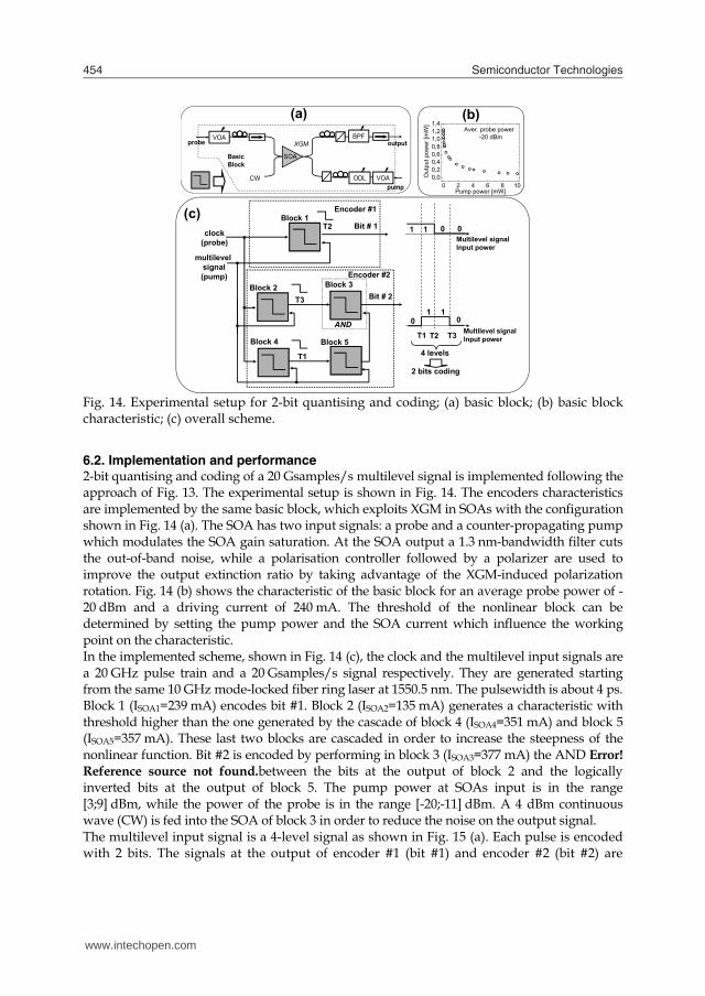
Fig. 14. Experimental setup for 2-bit quantising and coding; (a) basic block; (b) basic block characteristic; (c) overall scheme.
6.2. Implementation and performance 2-bit quantising and coding of a 20 Gsamples/s multilevel signal is implemented following the approach of Fig. 13. The experimental setup is shown in Fig. 14. The encoders characteristics are implemented by the same basic block, which exploits XGM in SOAs with the configuration shown in Fig. 14 (a). The SOA has two input signals: a probe and a counter-propagating pump which modulates the SOA gain saturation. At the SOA output a 1.3 nm-bandwidth filter cuts the out-of-band noise, while a polarisation controller followed by a polarizer are used to improve the output extinction ratio by taking advantage of the XGM-induced polarization rotation. Fig. 14 (b) shows the characteristic of the basic block for an average probe power of -20 dBm and a driving current of 240 mA. The threshold of the nonlinear block can be determined by setting the pump power and the SOA current which influence the working point on the characteristic. In the implemented scheme, shown in Fig. 14 (c), the clock and the multilevel input signals are a 20 GHz pulse train and a 20 Gsamples/s signal respectively. They are generated starting from the same 10 GHz mode-locked fiber ring laser at 1550.5 nm. The pulsewidth is about 4 ps. Block 1 (ISOA1=239 mA) encodes bit #1. Block 2 (ISOA2=135 mA) generates a characteristic with threshold higher than the one generated by the cascade of block 4 (ISOA4=351 mA) and block 5 (ISOA5=357 mA). These last two blocks are cascaded in order to increase the steepness of the nonlinear function. Bit #2 is encoded by performing in block 3 (ISOA3=377 mA) the AND Error! Reference source not found.between the bits at the output of block 2 and the logically inverted bits at the output of block 5. The pump power at SOAs input is in the range [3;9] dBm, while the power of the probe is in the range [-20;-11] dBm. A 4 dBm continuous wave (CW) is fed into the SOA of block 3 in order to reduce the noise on the output signal. The multilevel input signal is a 4-level signal as shown in Fig. 15 (a). Each pulse is encoded with 2 bits. The signals at the output of encoder #1 (bit #1) and encoder #2 (bit #2) are
www.intechopen.com
All-optical digital processing through semiconductor optical ampliiers: state of the art and perspectives 455
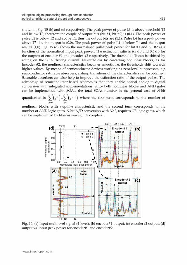
shown in Fig. 15 (b) and (c) respectively. The peak power of pulse L3 is above threshold T2 and below T3, therefore the couple of output bits (bit #1, bit #2) is (0,1). The peak power of pulse L2 is below T2 and above T1, thus the output bits are (1,1). Pulse L4 has a peak power above T3, i.e. the output is (0,0). The peak power of pulse L1 is below T1 and the output results (1,0). Fig. 15 (d) shows the normalised pulse peak power for bit #1 and bit #2 as a function of the normalised input peak power. The extinction ratio is 6.8 dB and 3.6 dB for the outputs of encoder #1 and encoder #2 respectively. The thresholds Ti can be shifted by acting on the SOA driving current. Nevertheless by cascading nonlinear blocks, as for Encoder #2, the nonlinear characteristics becomes smooth, i.e. the thresholds shift towards higher values. By means of semiconductor devices working as zero-level suppressors, e.g semiconductor saturable absorbers, a sharp transitions of the characteristics can be obtained. Saturable absorbers can also help to improve the extinction ratio of the output pulses. The advantage of semiconductor-based schemes is that they enable optical analog-to digital conversion with integrated implementations. Since both nonlinear blocks and AND gates can be implemented with SOAs, the total SOAs number in the general case of N-bit
quantisation is
1
1
11
022
N
n
nN
n
n where the first term corresponds to the number of
nonlinear blocks with step-like characteristic and the second term corresponds to the number of AND logic gates. N-bit A/D conversion with N>2, requires OR logic gates, which can be implemented by fiber or waveguide couplers.
50 ps/div
0
1
0
10 mV/div
50 ps/div
00
1
1
10 mV/div
50 ps/div
10 mV/div
T1 T2 T3
Input Signal
L3
L1
L2
L4
L3 L2 L4 L1
Encoder # 2 Output
Encoder # 1 Output
1
T1 T2 T3
(d)
(a)
(c)
(b)
0,0 0,2 0,4 0,6 0,8 1,00,0
0,2
0,4
0,6
0,8
1,0
Nor
mal
ized
out
put
peak
pow
er
Normalized input peak power
Bit # 1 Bit # 2
Fig. 15. (a) Input multilevel signal (4-level); (b) encoder#1 output; (c) encoder#2 output; (d) output vs. input peak power for encoder#1 and encoder#2.
www.intechopen.com
Semiconductor Technologies456
7. Digital-to-analog converter
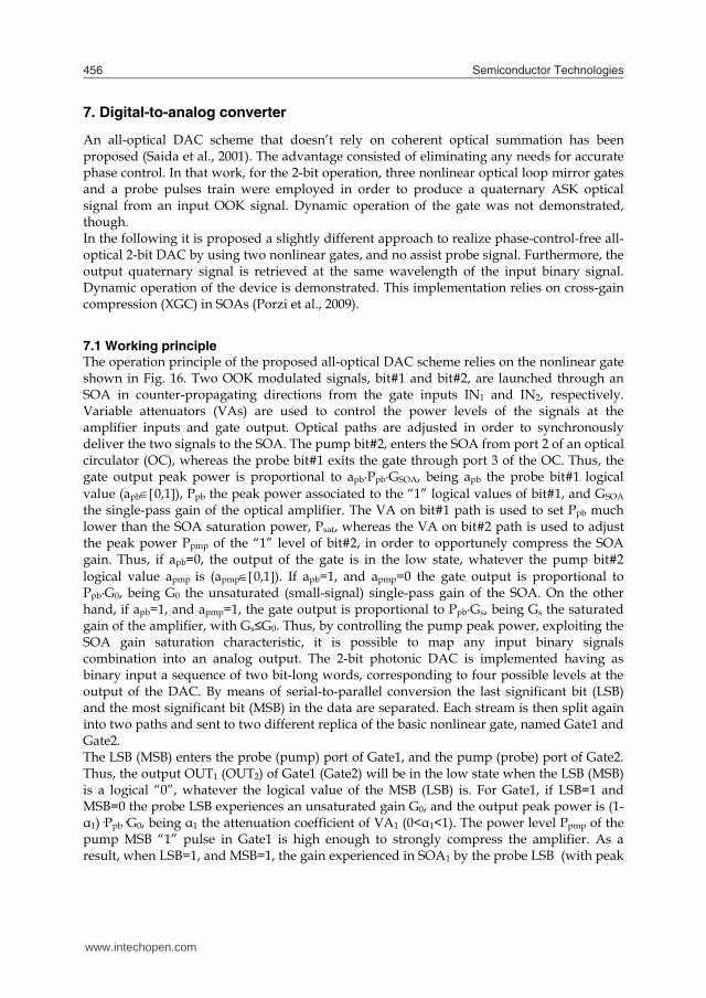
An all-optical DAC scheme that doesn’t rely on coherent optical summation has been proposed (Saida et al., 2001). The advantage consisted of eliminating any needs for accurate phase control. In that work, for the 2-bit operation, three nonlinear optical loop mirror gates and a probe pulses train were employed in order to produce a quaternary ASK optical signal from an input OOK signal. Dynamic operation of the gate was not demonstrated, though. In the following it is proposed a slightly different approach to realize phase-control-free all-optical 2-bit DAC by using two nonlinear gates, and no assist probe signal. Furthermore, the output quaternary signal is retrieved at the same wavelength of the input binary signal. Dynamic operation of the device is demonstrated. This implementation relies on cross-gain compression (XGC) in SOAs (Porzi et al., 2009). 7.1 Working principle The operation principle of the proposed all-optical DAC scheme relies on the nonlinear gate shown in Fig. 16. Two OOK modulated signals, bit#1 and bit#2, are launched through an SOA in counter-propagating directions from the gate inputs IN1 and IN2, respectively. Variable attenuators (VAs) are used to control the power levels of the signals at the amplifier inputs and gate output. Optical paths are adjusted in order to synchronously deliver the two signals to the SOA. The pump bit#2, enters the SOA from port 2 of an optical circulator (OC), whereas the probe bit#1 exits the gate through port 3 of the OC. Thus, the gate output peak power is proportional to apb·Ppb·GSOA, being apb the probe bit#1 logical value (apb0,1), Ppb the peak power associated to the “1” logical values of bit#1, and GSOA the single-pass gain of the optical amplifier. The VA on bit#1 path is used to set Ppb much lower than the SOA saturation power, Psat, whereas the VA on bit#2 path is used to adjust the peak power Ppmp of the “1” level of bit#2, in order to opportunely compress the SOA gain. Thus, if apb=0, the output of the gate is in the low state, whatever the pump bit#2 logical value apmp is (apmp0,1). If apb=1, and apmp=0 the gate output is proportional to Ppb·G0, being G0 the unsaturated (small-signal) single-pass gain of the SOA. On the other hand, if apb=1, and apmp=1, the gate output is proportional to Ppb·Gs, being Gs the saturated gain of the amplifier, with Gs≤G0. Thus, by controlling the pump peak power, exploiting the SOA gain saturation characteristic, it is possible to map any input binary signals combination into an analog output. The 2-bit photonic DAC is implemented having as binary input a sequence of two bit-long words, corresponding to four possible levels at the output of the DAC. By means of serial-to-parallel conversion the last significant bit (LSB) and the most significant bit (MSB) in the data are separated. Each stream is then split again into two paths and sent to two different replica of the basic nonlinear gate, named Gate1 and Gate2. The LSB (MSB) enters the probe (pump) port of Gate1, and the pump (probe) port of Gate2. Thus, the output OUT1 (OUT2) of Gate1 (Gate2) will be in the low state when the LSB (MSB) is a logical “0”, whatever the logical value of the MSB (LSB) is. For Gate1, if LSB=1 and MSB=0 the probe LSB experiences an unsaturated gain G0, and the output peak power is (1-α1)PpbG0, being α1 the attenuation coefficient of VA1 (0<α1<1). The power level Ppmp of the pump MSB “1” pulse in Gate1 is high enough to strongly compress the amplifier. As a result, when LSB=1, and MSB=1, the gain experienced in SOA1 by the probe LSB (with peak
www.intechopen.com
All-optical digital processing through semiconductor optical ampliiers: state of the art and perspectives 457
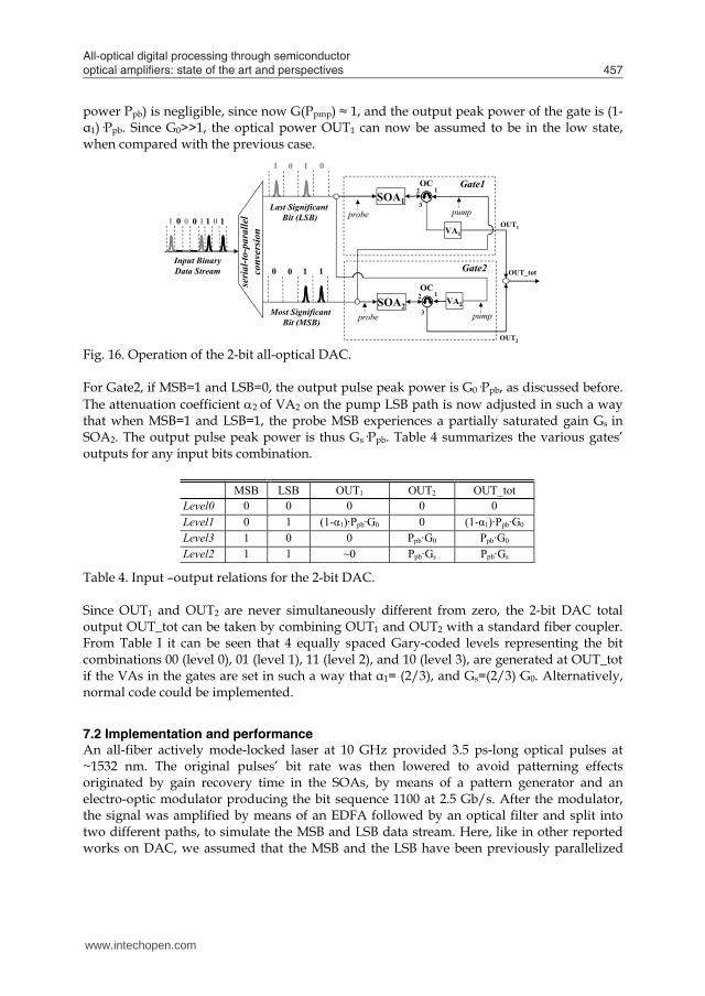
power Ppb) is negligible, since now G(Ppmp) ≈ 1, and the output peak power of the gate is (1-α1)Ppb. Since G0>>1, the optical power OUT1 can now be assumed to be in the low state, when compared with the previous case.
0 0 0 1 1 0 1
SOA1
OUT1
OUT2
seria
l-to-
para
llel
conv
ersio
nInput BinaryData Stream
Most SignificantBit (MSB)
Last SignificantBit (LSB)
probe
probe
pump
pump
SOA2
OUT_tot
Gate1
Gate2
OC12
3
3
OC12
1
1 0 1 0
0 1 1
VA1
VA2
0
Fig. 16. Operation of the 2-bit all-optical DAC. For Gate2, if MSB=1 and LSB=0, the output pulse peak power is G0Ppb, as discussed before. The attenuation coefficient 2 of VA2 on the pump LSB path is now adjusted in such a way that when MSB=1 and LSB=1, the probe MSB experiences a partially saturated gain Gs in SOA2. The output pulse peak power is thus GsPpb. Table 4 summarizes the various gates’ outputs for any input bits combination.
MSB LSB OUT1 OUT2 OUT_tot Level0 0 0 0 0 0 Level1 0 1 (1-α1)·Ppb·G0 0 (1-α1)·Ppb·G0 Level3 1 0 0 Ppb·G0 Ppb·G0 Level2 1 1 ~0 Ppb·Gs Ppb·Gs
Table 4. Input –output relations for the 2-bit DAC. Since OUT1 and OUT2 are never simultaneously different from zero, the 2-bit DAC total output OUT_tot can be taken by combining OUT1 and OUT2 with a standard fiber coupler. From Table I it can be seen that 4 equally spaced Gary-coded levels representing the bit combinations 00 (level 0), 01 (level 1), 11 (level 2), and 10 (level 3), are generated at OUT_tot if the VAs in the gates are set in such a way that α1= (2/3), and Gs=(2/3)G0. Alternatively, normal code could be implemented.
7.2 Implementation and performance An all-fiber actively mode-locked laser at 10 GHz provided 3.5 ps-long optical pulses at ~1532 nm. The original pulses’ bit rate was then lowered to avoid patterning effects originated by gain recovery time in the SOAs, by means of a pattern generator and an electro-optic modulator producing the bit sequence 1100 at 2.5 Gb/s. After the modulator, the signal was amplified by means of an EDFA followed by an optical filter and split into two different paths, to simulate the MSB and LSB data stream. Here, like in other reported works on DAC, we assumed that the MSB and the LSB have been previously parallelized
www.intechopen.com
Semiconductor Technologies458
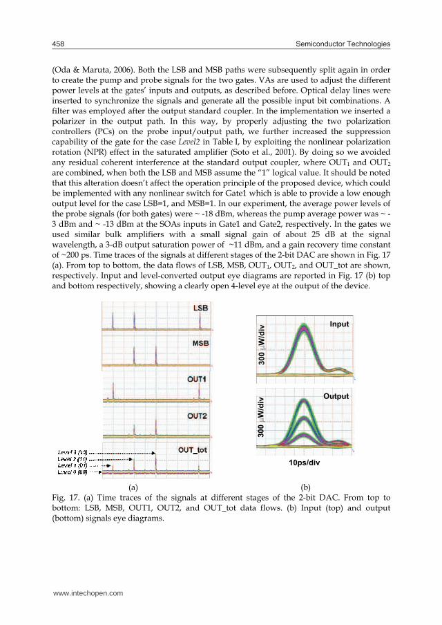
(Oda & Maruta, 2006). Both the LSB and MSB paths were subsequently split again in order to create the pump and probe signals for the two gates. VAs are used to adjust the different power levels at the gates’ inputs and outputs, as described before. Optical delay lines were inserted to synchronize the signals and generate all the possible input bit combinations. A filter was employed after the output standard coupler. In the implementation we inserted a polarizer in the output path. In this way, by properly adjusting the two polarization controllers (PCs) on the probe input/output path, we further increased the suppression capability of the gate for the case Level2 in Table I, by exploiting the nonlinear polarization rotation (NPR) effect in the saturated amplifier (Soto et al., 2001). By doing so we avoided any residual coherent interference at the standard output coupler, where OUT1 and OUT2 are combined, when both the LSB and MSB assume the “1” logical value. It should be noted that this alteration doesn’t affect the operation principle of the proposed device, which could be implemented with any nonlinear switch for Gate1 which is able to provide a low enough output level for the case LSB=1, and MSB=1. In our experiment, the average power levels of the probe signals (for both gates) were ~ -18 dBm, whereas the pump average power was ~ -3 dBm and ~ -13 dBm at the SOAs inputs in Gate1 and Gate2, respectively. In the gates we used similar bulk amplifiers with a small signal gain of about 25 dB at the signal wavelength, a 3-dB output saturation power of ~11 dBm, and a gain recovery time constant of ~200 ps. Time traces of the signals at different stages of the 2-bit DAC are shown in Fig. 17 (a). From top to bottom, the data flows of LSB, MSB, OUT1, OUT2, and OUT_tot are shown, respectively. Input and level-converted output eye diagrams are reported in Fig. 17 (b) top and bottom respectively, showing a clearly open 4-level eye at the output of the device.
Input
Output
300
W/d
iv
10ps/div
300
W/d
iv
(a) (b) Fig. 17. (a) Time traces of the signals at different stages of the 2-bit DAC. From top to bottom: LSB, MSB, OUT1, OUT2, and OUT_tot data flows. (b) Input (top) and output (bottom) signals eye diagrams.
www.intechopen.com
All-optical digital processing through semiconductor optical ampliiers: state of the art and perspectives 459
To the best of our knowledge, this is the first time that dynamic operation for a phase-control-free 2-bit all-optical DAC is experimentally demonstrated for single wavelength operation. We measured the Q factors for the input and level-converted output signals by taking the histograms of noise distributions with a standard sampling oscilloscope with 10-GHz of bandwidth. The input binary signal Q factor was measured to be 22, whereas the output Q factors were measured to be 10.2, 9.8, and 10.9 for level1-to-level0, level2-to-level1, and level3-to-level2 eyes, respectively.
8. References
Abbade M. L. F., Fagotto E. A. M., Braga R. S., Fonseca I. E., Moschim E. & Barbosa F. R., (2005). Optical Amplitude Multiplexing Through Four-Wave Mixing in Optical Fibers. IEEE Photonics Technology Letters, Vol. 17 No. 1 (Jan. 2005) pp. 151-153, 1041-1135.
Abbade M. L. F., Fagotto E. A. M., Braga R. S., Barbosa F. R., Moschim E. & Fonseca I. E., (2006). Quaternary Optical Packets Generated by Fiber Four-Wave Mixing. IEEE Photonics Technology Letters, Vol. 18 No. 2 (Jan. 2006) pp. 331-333, 1041-1135.
Andriolli N.,Scaffardi M., Berrettini G., Potì L. & Bogoni A.,(2007). Multistage interconnection network photonic controller exploiting a cascaded SOA-based ultrafast module. Proceedings of ECOC’07, P117, 978-3-8007-3059-9, Berlin, Germany, 16-20 September 2007.
Berrettini G., Simi A., Malacarne A., Bogoni A., & Poti L., (2006). Ultrafast Integrable and Reconfigurable XNOR, AND, NOR, and NOT Photonic Logic Gate. IEEE Photonics Technology Letters, Vol. 18 No. 8 (Apr. 2006) pp. 917-919, 1041-1135.
Berrettini G.,. Lauri E, Ghelfi P., Bogoni A. & Potì L., (2006). Ultra-Fast Integrable 2x2 All-Optical Switch for Optical Packet Routing. Proceedings of ECOC’06, We3.P.102, 978-2-912328-39-7, Cannes, France, 24-28 Sept. 2006.
Bogoni, A.; Poti, L.; Proietti, R.; Meloni, G.; Ponzini, E. & Ghelfi, P., (2005). Regenerative and Reconfigurable All-Optical Logic Gates for Ultra-Fast Applications. IEE Electronics Letters, Vol. 41, No, 7, (Mar. 2005) pp.435-436, 0013-5194.
L. Brzozowski & E. H. Sargent, (2001). All-optical analog-to-digital converters, hardlimiters, and logic gates. IEEE Journal of Lightwave Technology, Vol. 19, No. 1, (Jan. 2001) pp. 114–119, 0733-8724.
Chbat M. W.; Hong B. J.; Islam M. N., Coccoloch C. E. & Prucnal A. L., (1992). Ultrafast soliton-trapping AND gate. IEEE Journal of Lightwave Technology, Vol. 10, No. 12, (Dec. 1992) pp. 2011-2016, 0733-8724.
Chan L. Y., Qureshi K. K., Wai P. K. A., Moses B., Lui L. F. K., Tam H. Y. & Demokan M. S., (2003). All-Optical Bit-Error Monitoring System Using Cascaded Inverted Wavelength Converter and Optical NOR Gate. IEEE Photonics Technology Letters, Vol. 15 No. 4 (Apr. 2003) pp. 593-595, 1041-1135.
Cheng W., Ali W., Choi M.-J., Liu K., Tat T., Devendorf D., Linder L. & Stevens R., (2004). A 3b 40 Gsamples/s ADC-DAC in 0.12 μm SiGe. Proceedings of IEEE Int. Solid-State Circuits Conference, Vol. 1, pp. 262–263, 0-7803-8267-6, San Francisco, California, USA, 15-19 Feb. 2004.
www.intechopen.com
Semiconductor Technologies460
Collecutt, G.R. & Drummond, P.D., (2000). Digital response in an all optical AND gate using parametric (χ (2)) solitons. Proceedings of CLEO’00, pp. 194, 1-55752-634-6, San Francisco, California, USA, 7-12 May 2000.
Dorren H. J. S., Lenstra D., Liu Y., Hill M. T. & Khoe G.-D., (2003). Nonlinear polarization rotation in semiconductor optical amplifiers: theory and application to all-optical flip-flop memories. IEEE Journal of Quantum Electronics, Vol. 39, No. 1, (Jan 2003) pp. 141-148, 0018–9197.
Dorren, H.J.S.; Mishra, A.K.; Li, Z.G.; Ju, H.K.; de Waardt, H.; Khoe, G.D.; Simoyama, T.; Ishikawa, H.; Kawashima, H. & Hasama, T., (2004). All-optical logic based on ultrafast gain and index dynamics in a semiconductor optical amplifier. IEEE Selected Topics in Quantum Electronics, Vol. 10, No. 5, (Sept./Oct. 2004) pp. 1079-1092, 1077-260X.
Fok M. P., Lee K. L. & Shu C., (2004). 4 2.5 GHz Repetitive Photonic Sampler for High-Speed Analog-to-Digital Signal Conversion. IEEE Photonics Technology Letters, Vol. 16 No. 3 (Mar. 2004) pp. 876-878, 1041-1135.
Forney G. D., (1973). The Viterbi algorithm. Proceedings of IEEE, Vol. 61, No. 3, (Mar. 1973) pp. 268–278, 0018-9219.
Hall K. L. & Rauschenbach K. A., (1996). All-optical bit pattern generation and matching. IEE Electronics Letters, Vol. 32, No, 13, (Jun. 1996) pp. 1214-1215, 0013-5194.
Hayes J. P., (1998). Computer Architecture and Organization. McGraw-Hill, 0-07-100479-3, New York.
Ibrahim, T.A.; Grover, R.; Kuo, L.C.; Kanakaraju, S.; Calhoun, L.C. & Ho, P.T., (2003). All-optical AND/NAND logic gates using semiconductor microresonators. IEEE Photonics Technology Letters, Vol. 15, No. 10, (Oct. 2003) pp. 1422-1424, 1041-1135.
Ikeda K., Abdul J. M., Tobioka H., Inoue T., Namiki S. & Kitayama K., (2006). Design Considerations of All-Optical A/D Conversion: Nonlinear Fiber-Optic Sagnac-Loop Interferometer-Based Optical Quantizing and Coding. IEEE Journal of Lightwave Technology, Vol. 24, No. 7, (Jul. 2006) pp. 2618-2628, 0733-8724.
Kehayas E., Seoane J., Liu Y., Martinez J. M., Herrera J., Holm-Nielsen P. V., Zhang S., McDougall R., Maxwell G., Ramos F., Marti J., Dorren H. S. J., Jeppesen P. & Avramopoulos H., (2006). All-Optical Network Subsystems Using Integrated SOA-Based Optical Gates and Flip-Flops for Label-Swapped Networks. IEEE Photonics Technology Letters, Vol. 18 No. 16 (Aug. 2006) pp. 1750-1752, 1041-1135.
Kehayas E. Tsiokos, D.I., Bakopoulos, P., Apostolopoulos, D., Petrantonakis, D., Stampoulidis, L., Poustie, A., McDougall, R., Maxwell, G., Liu, Y., Zhang, S. X., Dorren, H.J.S., Seoane, J., Van Holm-Nielsen, P., Jeppesen, P. & Avramopoulos, H., (2006). 40-Gb/s all-optical processing systems using hybrid photonic integration technology. IEEE Journal of Lightwave Technology, Vol. 24, No. 12, (Dec. 2006) pp. 4903-4911, 0733-8724.
Kim J. H., Jhon Y. M., Byun Y. T., Lee S., Woo D. H. & Kim S. H., (2002). All-optical XOR gate using semiconductor optical amplifiers without additional input beam. IEEE Photonics Technology Letters, Vol. 14 No. 10 (Oct. 2002) pp. 1436-1438, 1041-1135.
Kim J. H., Kim B. C., Byun Y. T., Jhon Y. M., Lee S., Woo D. H. & Kim S. H., (2003). All-optical full adder using semiconductor optical amplifiers. Proceedings of ECOC’03, We4.P75, Rimini, Italy, 21-25 Sept. 2003.
www.intechopen.com
All-optical digital processing through semiconductor optical ampliiers: state of the art and perspectives 461
Konishi T., Tanimura K., Asano K., Oshita Y. & Ichioka Y., (2002). All-optical analog-to-digital converter by use of self-frequency shifting in fiber and a pulse-shaping technique. Jornal of the Optical Society of American B, Vol. 19, No. 11, (Nov. 2002), pp. 2817-2823, 0740-3224.
Kumar S. & Willner A. E., (2004). All optical gate using simultaneous four-wave mixing and cross-gain modulation in an SOA. Proceedings of LEOS’04, pp. 913, 0-7803-8557-8, Westin Rio Mar Beach, Rio Grande, Puerto Rico, 7-11 Nov 2004.
Lal V., Masanovic, M.L., Summers, J.A., Fish, G. & Blumenthal, D.J., (2007). Monolithic wavelength converters for high-speed packet-switched optical networks. IEEE Selected Topics in Quantum Electronics, Vol. 13, No. 1, (Jan./Feb. 2007) pp. 49-57, 1077-260X.
Li W., Zhang H., Wu Q., Zhang Z. & Yao M., (2005). All-Optical Analog-to-Digital Conversion Based on Polarization-Differential Interference and Phase Modulation. IEEE Photonics Technology Letters, Vol. 19 No. 8 (Apr. 2005) pp. . 625-627, 1041-1135.
Liu, Y., Tangdiongga, E., Li, Z., de Waardt, H., Koonen, A. M. J., Khoe, G. D., Shu, X., Bennion, & Dorren, H. J. S., (2007). Error-free 320-Gb/s all-optical wavelength conversion using a single semiconductor optical amplifier. IEEE Journal of Lightwave Technology, Vol. 25, No. 1, (Jan. 2007) pp. 103-108, 0733-8724.
Malacarne A., Bogoni A. & Potì L., (2006). An Optical Flip-Flop Based on Erbium-Ytterbium Doped Fibre. Proceedings of ECOC’06, We3.P.31, 978-2-912328-39-7, Cannes, France, 24-28 Sept. 2006.
Martinez M., Herrera J., Ramos F. & Marti J., (2006). All-optical address recognition scheme for label-swapping networks. IEEE Photonics Technology Letters, Vol. 18 No. 1 (Jan. 2006) pp. 151-153, 1041-1135.
Maxwell G., (2008). Hybrid Integration Technology for High Functionality Devices in Optical Communications. Proceedings of OFC’08, OWI3, 978-1-55752-856-8, San Diego, California, USA, 24-28 February 2008.
McGeehan, J.E.; Kumar, S.; Gurkan, D.; Nezam, S.M.R.M.; Willner, A.E.; Parameswaran, K.R.; Fejer, M.M.; Bannister, J. & Touch, J.D. (2003). All-optical decrementing of a packet’s Time-to-Live (TTL) field and subsequent dropping of a zero-TTL packet. IEEE Journal of Lightwave Technology, Vol. 21, No. 11, (Nov. 2003) pp. 27466-2752, 0733-8724.
Miyoshi Y., Ikeda K., Tobioka H., Inoue T., Namiki S. & Kitayama K., (2007). All-Optical Analog-to-Digital Conversion Using Split-and-Delay Technique. IEEE Journal of Lightwave Technology, Vol. 25, No. 6, (Jun. 2007) pp. 1339-1347, 0733-8724.
Nielsen M. L., Fjelde T., Buron J. D. & Dagens B., (2002). All-optical bit-pattern recognition in data segments using logic AND and XOR in a single all-active MZI wavelength converter. Proceedings of ECOC’02, 1.4.6, 87-90974-63-8, Copenhagen, Denmark, 8-12 Sept. 2002.
Nishitani T., Konishi T. & Itoh K., (2008). Resolution Improvement of All-Optical Analog-to-Digital Conversion Employing Self-frequency Shift and Self-Phase-Modulation-Induced Spectral Compression. IEEE Selected Topics in Quantum Electronics, Vol. 14, No. 3, (May/Jun. 2008) pp. 724-732, 1077-260X.
Oda S. & Maruta A., (2005). A Novel Quantization Scheme by Slicing Supercontinuum Spectrum for All-Optical Analog-to-Digital Conversion. IEEE Photonics Technology Letters, Vol. 17 No. 2 (Feb. 2005) pp. . 465-467, 1041-1135.
www.intechopen.com
Semiconductor Technologies462
Oda S. & Maruta A., (2006). All-Optical Digital-to-Analog Conversion Using Nonlinear Optical Loop Mirrors. IEEE Photonics Technology Letters, Vol. 18 No. 5 (Mar. 2006) pp. 703-705, 1041-1135.
Porzi, C., Nguyen, A.T., Poti, L. & Bogoni, A., (2009). Binary-to-Quaternary ASK Encoding in the Optical Domain With Semiconductor Optical Amplifiers. IEEE Photonics Technology Letters, Vol. 21 No. 10 (May. 2009) pp. 654 - 656, 1041-1135.
Poustie A.J., Blow K.J., Kelly A.E. & Manning R.J., (1999). All-optical full adder with bit-differential delay. Optics Communications, Vol. 168, (Sept. 1999) pp. 89-93, 0030-4018.
Proakis J. G., (1996). Digital Communications, McGraw-Hill, 978-0072321111, New York. Saida T., Okamoto K., Uchiyama K.,. Takiguchi K, Shibata T. & Sugita A., (2001). Integrated
optical digital-to-analogue converter and its application to pulse pattern recognition. IEE Electronics Letters, Vol. 37, No, 20, (Sept. 2001) pp. 1237-1238, 0013-5194.
Scaffardi, M; Andriolli, N; Meloni, G; Berrettini, G; Fresi, F; Castoldi, P (; Poti, L & Bogoni, A., (2007). Photonic combinatorial network for contention management in 160 Gb/s interconnection networks based on all-optical 22 switching elements. IEEE Selected Topics in Quantum Electronics, Vol. 13, No. 5, (Sept./Oct. 2007) pp. 1531- 1539, 1077-260X.
Scaffardi, M.; Ghelfi, P.; Lazzeri, E.; Poti, L. & Bogoni, A., (2008). Photonic processing for digital comparison and full addition based on semiconductor optical amplifiers. IEEE Selected Topics in Quantum Electronics, Vol. 14, No. 3, (May./Jun. 2008) pp. 826-833, 1077-260X.
Scaffardi, M; Lazzeri, E.; Fresi, F. ; Poti, L. & Bogoni, A, (2009). Analog-to-Digital Conversion Based on Modular Blocks Exploiting Cross-Gain Modulation in Semiconductor Optical Amplifiers. IEEE Photonics Technology Letters, Vol. 21 No. 8 (Apr. 2009) pp. 540-542, 1041-1135.
Shacham, A.; Small, B.A.; Liboiron-Ladouceur & O.; Bergman, K., (2005). A fully implemented 12x12 data vortex optical packet switching interconnection network. IEEE Journal of Lightwave Technology, Vol. 23, No. 10, (Oct. 2005) pp. 3066-3075, 0733-8724.
Soto H., Erasme D. & Guekos G., (1999). Cross-polarization modulation in semiconductor optical amplifiers. IEEE Photonics Technology Letters, Vol. 11 No. 8 (Aug. 1999) pp970-972, 1041-1135.
Soto H., Erasme D. & Guekos G., (2001). 5-Gb/s XOR optical gate based on cross-polarization modulation in semiconductor optical amplifiers. IEEE Photonics Technology Letters, Vol. 13 No. 4 (Apr. 2001) pp. 335-337, 1041-1135.
Tangdiongga E., Hansen Mulvad H.C., de Waardt H., Khoe G.D., Koonen A.M.J. & Dorren H.J.S., (2007). SOA-based Clock Recovery and Demultiplexing in a Lab Trial of 640-Gb/s OTDM and Demultiplexing in a Lab Trial of 640-Gb/s OTDM Transmission over 50-km Fibre Link. Proceedings of ECOC’07, PD 1.2, 978-3-8007-3059-9, Berlin, Germany, 16-20 September 2007.
Wada N., Cincotti G., Yoshima S., Kataoka N. & Kitayama K., (2006). Characterization of a full encoder/decoder in the AWG configuration for code-based photonic routers—part II: experiments and Applications. IEEE Journal of Lightwave Technology, Vol. 24, No. 1, (Jan. 2006) pp. 113-121, 0733-8724.
www.intechopen.com

All-optical digital processing through semiconductor optical ampliiers: state of the art and perspectives 463
Walden R. H., (1999). Analog-to-Digital Converter Survey and Analysis. IEEE Journal on Selected Areas in Communications, Vol. 17, No. 4, (Apr. 1999) pp. 539-550, 0733-8716.
Wang Y., Zhang X., Dong J. & Huang D., (2007). Simultaneous demonstration on all-optical digital encoder and comparator at 40 Gb/s with semiconductor optical amplifiers. Optics Express, Vol. 15, No. 23, (Nov. 2007) pp. 15080-15085, 1094-4087.
Wu Y. D., (2005). All-optical logic gates by using multibranch waveguide structure with localized optical nonlinearity. IEEE Selected Topics in Quantum Electronics, Vol. 11, No. 2, (Mar. 2005) pp. 307-312, 1077-260X.
Yacoubian A. & Das P. K., (2003). Digital-to-Analog Conversion Using Electrooptic Modulators. IEEE Photonics Technology Letters, Vol. 15 No. 1 (Jan. 2003) pp. 117-119, 1041-1135.
www.intechopen.com

Semiconductor Technologies464
www.intechopen.com

Semiconductor TechnologiesEdited by Jan Grym
ISBN 978-953-307-080-3Hard cover, 462 pagesPublisher InTechPublished online 01, April, 2010Published in print edition April, 2010
InTech EuropeUniversity Campus STeP Ri Slavka Krautzeka 83/A 51000 Rijeka, Croatia Phone: +385 (51) 770 447 Fax: +385 (51) 686 166www.intechopen.com
InTech ChinaUnit 405, Office Block, Hotel Equatorial Shanghai No.65, Yan An Road (West), Shanghai, 200040, China
Phone: +86-21-62489820 Fax: +86-21-62489821
Semiconductor technologies continue to evolve and amaze us. New materials, new structures, newmanufacturing tools, and new advancements in modelling and simulation form a breeding ground for novelhigh performance electronic and photonic devices. This book covers all aspects of semiconductor technologyconcerning materials, technological processes, and devices, including their modelling, design, integration, andmanufacturing.
How to referenceIn order to correctly reference this scholarly work, feel free to copy and paste the following:
Gianluca Berrettini, Antonella Bogoni, Emma Lazzeri, Gianluca Meloni, Claudio Porzi, Luca Poti and MircoScaffardi (2010). All-optical Digital Processing Through Semiconductor Optical Amplifiers, SemiconductorTechnologies, Jan Grym (Ed.), ISBN: 978-953-307-080-3, InTech, Available from:http://www.intechopen.com/books/semiconductor-technologies/all-optical-digital-processing-through-semiconductor-optical-amplifiers

© 2010 The Author(s). Licensee IntechOpen. This chapter is distributedunder the terms of the Creative Commons Attribution-NonCommercial-ShareAlike-3.0 License, which permits use, distribution and reproduction fornon-commercial purposes, provided the original is properly cited andderivative works building on this content are distributed under the samelicense.