2017 international conference on microelectronic …
TRANSCRIPT
A Statistical Modeling Methodology of RTN GateSize Dependency Based on Skewed Ring Oscillators
A.K.M. Mahfuzul Islam⇤, Tatsuya Nakai†, and Hidetoshi Onodera†⇤ Institute of Industrial Science, The University of Tokyo, 4-6-1 Komaba, Meguro-ku, Tokyo 153-8505, JAPAN.
e-mail: [email protected]: +81-3-5452-6253, Fax: +81-3-552-6632
† Graduate School of Informatics, Kyoto University, Yoshida-honmachi, Sakyo-ku, Kyoto 606-8501, JAPAN.e-mail: {tnakai,onodera}@vlsi.kuee.kyoto-u.ac.jp
Tel: +81-75-753-5353, Fax: +81-75-753-5343
Abstract—This paper proposes a statistical modeling method-ology of RTN (Random Telegraph Noise) gate size dependencyutilizing skewed ring oscillator (RO) structures. An iterativecharacterization flow is developed to estimate RTN inducedthreshold distribution of each gate sizes of pMOSFET andnMOSFET independently. The skewed RO based test structurewas fabricated in a 65 nm SOTB (Silicon On Thin Body) process.It is observed that Lognormal distribution represents RTN in-duced delay distribution well. RTN model of gate size dependencyis then developed and validated using the measured data. Modelbased delay distribution estimation and measurement matchwell. The proposed extraction methodology is thus suitable forestimating RTN of transistors with arbitrary gate size. The modelhelps reliability and worst case analysis of digital circuits wheretransistors of various gate sizes are used.
I. INTRODUCTION
With technology scaling, RTN induced threshold voltagevariation �VT is becoming significant [1]. There are reportsof RTN in SRAMs [2], ring oscillators (RO) [3], and Flashmemories [4]. At low voltage operation, frequency fluctuationof 10.4 % has been reported for a 40 nm process [3]. AsRTN induced �VT distribution has long tails, worst case delaydegradation is severe compared with process variation. In adigital circuit, transistors of different gate sizes and lengthsare used to optimize delay and power. For design time opti-mization and reliability analysis, RTN models incorporatingchannel width and length dependencies are required. In thispaper, we focus on RTN modeling of gate size dependencybased on delay measurement. We propose a test structurecomprised of an array of ring oscillators (RO) with differentskewed inverters. We build RTN models for pMOSFET andnMOSFET separately that can be applied to transistor of arbi-trary sizes. This eliminates the need to characterize transistorRTN for each of the gate sizes used in a standard cell library.
As RTN is a statistical phenomena and have dynamic nature,measurement and characterization of RTN consumes time.Transistor I–V based characterization is the most commonmethod [5]. However, in a digital circuit environment, thetransistors operate under switching conditions. Therefore, anembedded test structure in a digital circuit will provide in-situ RTN properties of switching behavior. For example dis-tribution of total �VT amplitude due to complex RTN can
differ from convolution of individual trap �VT distribution[6]. RO based delay fluctuation measurement can be used tocharacterize RTN properties under switching conditions [3].To enable transistor level characterization of RTN using ROs,tuning of the inverter topology [7] or the transistor sizes areperformed so that measured delay variation can be relatedto a particular transistor [8]. This gives us in-situ charac-terization of transistor RTN under switching conditions. Wehave proposed such RO structures and their characterizationmethodology in Refs. [7, 9]. A topology reconfigurable ROstructure can be used to further amplify RTN effects of thetarget transistors [9].
In the RO structures mentioned above, transistor sizingneeds to be tuned such that the delay fluctuation can beattributed only to a particular transistor. The required sizingratio varies depending on the RTN distribution spread. Alarge spread will require a larger sizing ratio. Another keyfeature to emulate actual digital circuit behavior is to evaluatemulti-stage delay instead of a single stage. A homogeneousstructure rather than an inhomogeneous structure is thus morerepresentative of a digital circuit behavior. However, using ahomogeneous structure, obtaining transistor level �VT dis-tribution is difficult as other transistors in the RO contributeto overall delay fluctuation. In this paper, we propose a newcharacterization methodology that utilizes the convolution andde-convolution operations to sum or deduct distributions, andshow that the methodology can be used to estimate efficienttransistor level RTN models using the homogeneous structures.
Our goal is to build RTN models for pMOSFET andnMOSFET separately that incorporates transistor gate sizedependency similar to the one used for modeling static �VT
variation known as the Pelgrom model [10]. We find that theamount of overall fluctuation can be modeled by a Lognormaldistribution. As the Lognormal distribution has two parame-ters, we evaluate their size dependency, and develop a modelthat can be used to predict RTN for arbitrary size transistor.
We describe our test structure and its design methodologyis Sec. II. We then describe our proposed statistical modelingmethodology for gate size dependency extraction. We presentand discuss the measurement results in Sec. III. We put ourconcluding remarks in Sec. IV.
2017 INTERNATIONAL CONFERENCE ON MICROELECTRONIC TEST STRUCTURES, MARCH 28-30, GRENOBLE, FRANCE 8.1
978-1-5090-3615-8/17 $31.00 © 2017 IEEE

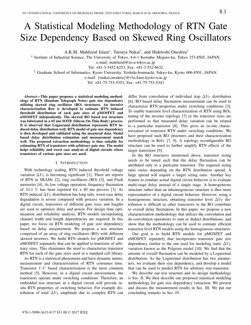
(a)
80x
1x2x4x16x
80x
16x
80x
4x
80x
80x
2x
80x
80x
1x
80x(b)
Fig. 1: Concept of skewed inverter design for RTN gate sizedependency modeling. (a) pMOSFET dominant, (b) nMOS-FET dominant.
II. CHARACTERIZATION AND MODELING METHODOLOGY
A. Test Structure Design Methodology
In this paper, we show that skewed inverters of differentratios can be utilized to build RTN model for gate sizedependency. Fig. 1 shows the design methodology of skewedinverters. Two series of skewed inverters are used. In oneseries, pMOSFET is larger than the nMOSFET and vice versa.The key point here is to keep the larger MOSFET size sameand change the smaller transistor size ratios so that a singledistribution can be used for the larger transistor across theROs. If we have a sufficient model to estimate the delaycontribution from larger transistors, delay contribution fromthe smaller transistors can be estimated by de-convolvinglarger transistor distribution from the total �D distribution.Iterating and updating the RTN gate size dependency modelwill eventually converge to a point where distributions of allROs are fitted well. We then obtain our final RTN gate sizeddependency model.
B. RTN Induced Delay Distribution
In evaluating the total variation, we use the maximum andminimum values and take their differences.
�D = DMAX �DMIN. (1)
In a homogeneous RO structure, all the inverter stagesshare the same topology. We use skewed inverters in thistest structure where we denote �VT distribution for thesmaller transistor as VTARGET. VOTHER is used to representdistribution for the larger transistor. Multiple RO instances ofthe same ratio are measured to obtain the distributions. Totaldelay distribution ZMEAS can be expressed as the sum of dis-tributions contributed by both the smaller and larger transistors
Prob
abili
ty
Normalized delay variation0 0.2 0.4 0.6 0.8 10
10
20
30
40
50
Contribution from pMOSFET (6000 nm)
Contribution from nMOSFET (1120 nm)
Total delay
Fig. 2: Contributions of transistors in a RO to total delaydistribution. Total delay distribution is the convolution of twodelay distributions caused by noises. One distribution is causedby the RTN in the smaller nMOSFET. The other distributionis caused by the larger pMOSFETs.
as in (4). The delay contributions from each transistor can bemodeled by multiplying sensitivity coefficient to �VT.
XTARGET =
X
i
kiTARGET · V iTARGET, (2)
XOTHER =
X
i
kiOTHER · V iOTHER, (3)
ZMEAS = XTARGET +XOTHER. (4)
Here, XTARGET is the delay distribution contributed by thesmall transistors. XOTHER is the delay distribution contributedby the large transistors. kiTARGET and kiOTHER are sensitivitycoefficients. V i
TARGET and V iOTHER represent distributions
for the i-th stage transistors. ZMEAS is the measured delaydistribution.
Fig. 2 shows simulated probability distribution functions(PDF) of XTARGET, XOTHERS and ZMEAS for a RO wheregate sizes of nMOSFET and pMOSFET are 1120 nm and6000 nm, respectively. From the figure, MOSFETs with largergate size have significant impact on the overall delay distri-bution. Thus, �VT distribution for the smaller transistor sizecannot be extracted accurately from this RO only. One solutioncan be to use very high size ratios for the skewed inverter.However, the required size ratio is not fixed and may result ina unrealistic value if the RTN is high for the target process.Instead, we propose an iterative statistical method which doesnot rely on specific size ratios to extract �VT distributions.This is performed by modeling the gate size dependency andutilizing the fact that total distribution is a convolution ofdistributions from smaller and larger transistors.
C. Extraction of �VT Distribution
As we obtain delay distributions using RO based test struc-tures, we need to extract �VT distributions from measured

Estimate smallTr. distribution
Distributions
Distribution fitting
Sensitivitycoefficients
Simulation
Measurement
Build RTN modelσ∝ kσ /Wa, µ′ ∝ kµ/Wb
Estimate largeTr. distribution
Subtract largeTr. Contribution
(Initial contribution = 0)
Converge? Final RTN modelYes
No
Fig. 3: Proposed characterization flow.
delay distributions. In order to do that, we first approximatetotal delay variation as follows.
�D ⇡X
ki�VT,i. (5)
Here, ki is sensitivity coefficient and �VTi is RTN induced�VT fluctuation for a particular transistor. Now, if �VT
follows Lognormal distribution lnN (µ,�2), then ki�VT will
follow lnN (µ + ln ki,�2). This refers that for the same
transistor size, the delay contribution contributed by transistorsof different sensitivity coefficient values can be expressedby Lognormal distributions of the same � value. As sumof Lognormal distributions can be approximated by anotherLognormal distribution, we can derive µz and �z of themeasured delay distribution as in (6) [11, 12].
�2z ⇠ ln
(e�
2
� 1)
Pk2j
(
Pkj)2
+ 1
!,
µz ⇠ µ+
�2
2
� �2z
2
+ ln(
Xkj). (6)
Thus, measured distribution parameters µz and �z can beexpressed by the terms of µ, � and kj . Solving (6) for µand �, we obtain these values with (8) . Thus, �VT distribu-tion is obtained from �D distributions given the sensitivitycoefficients of each transistor in the RO.
�2 ⇠ ln
✓exp(�2
z)� 1
Ck1+ 1
◆, Ck1 =
Pk2j
(
Pkj)2
, (7)
µ ⇠ µz ��2
2
+
�2z
2
� ln(
Xkj). (8)
D. RTN Characterization Flow
We propose a modeling methodology shown in Fig. 3 thatincorporates RTN contributions from both the smaller and
larger transistors. Using Lognormal models to represent the�D and �VT distributions, convolution and de-convolution ofPDFs are used to obtain sum and difference between multipledistributions. An iterative flow is used which update the RTNmodel at each iteration.
At the beginning of the flow, Lognormal distribution param-eters of µz and �z are fitted with the measured �D distributionfor each RO. Then, Lognormal distribution parameters of µand � of the �VT distribution are estimated using (8). In thefirst iteration, we consider that RTN of each RO is contributedby the smaller transistors only ignoring the larger transistors.Therefore, RTN of each RO is attributed to smaller transistorswith different gate sizes. RTN of an RO where pMOSFET issmaller than nMOSFET is attributed to pMOSFET and viceversa. Thus, we obtain Lognormal distribution parameters fordifferent gate sizes of pMOSFET and nMOSFET, respectively.The µ and � values of �VT distributions for each gate sizeare then fitted against a model that incorporates gate sizedependency as shown in (9) and (10).
µ = ln µ̂ = ln
✓kµW aµ
◆, (9)
� =
k�W a�
. (10)
One key point to note in (9) is that logarithm is used to modelgate size dependency. This is to make sure that with gate sizeapproaching infinity, �VT spread approaches zero. Althoughcontributions from the larger transistors were ignored at thefirst iteration, these contributions are taken into account sincethe second iteration forward. We estimate these contributionsusing the models of (9) and (10) that are obtained at the endof the previous iteration. Since the second iteration forward,as we have estimations for larger transistor contributions, wededuct these contributions and re-evaluate the �VT distribu-tions for the smaller transistors. After several iterations, allthe distribution parameter values converges to fixed values.Finally, we obtain �VT distributions for each transistor sizeof pMOSFET and nMOSFET. In this study, our flow convergesafter the fourth iteration.
III. MEASUREMENT AND RESULTS
A. Test Structure
Fig. 4 shows our test structure in a 65 nm SOTB (Siliconon Thin Body) process consisting of an array of RO blocks.There are 150 blocks in a chip. Therefore, we obtain 150
samples for each RO type. Each block consists of multiple ROswith different skewed inverters. Transistor sizing used in theskewed inverters are shown in the table. There are two types ofskewed inverters. One type has smaller nMOSFET and largerpMOSFET. The other type has smaller pMOSFET and largernMOSFET. Smaller transistor size in each inverter type isvaried to four different sizes to evaluate gate size dependency.Fig. 5 shows chip micrograph of our test structure.
As RTN is a time-dependent phenomena, the all RO in-stances are measured for 12 s of time. The oscillation signal

EN
EN
EN
EN
Large P
Small N
Small P
Large N
Array of RO blocks
nMOSFETgate size (µm)
pMOSFETgate size (µm)
#1 140 10480#2 280 10480#3 560 10480#4 1120 10480#5 6720 140#6 6720 280#7 6720 560#8 6720 1120#9 6720 10480
Fig. 4: An array of ROs to evaluate transistor noise of variousgate widths.
Fig. 5: Chip micrograph.
for each circuit is integrated for about 2 ms and then measuredwith a clock signal of 24 MHz frequency.
B. Delay Distributions
Figs. 6 and 7 shows two samples of oscillation periodfluctuation over 12 s of time. Fig. 8 shows measured delaydistributions for four ROs where pMOSFET is much smallerthan nMOSFET. pMOSFETs of four different sizes are usedhere. Delay distribution follows Lognormal distribution. Fig. 9shows delay distributions for ROs with four different nMOS-FETs where nMOSFET is much smaller than pMOSFET. Inthis study, we focus on the total delay variation, thus we donot extract single trap induced RTN. The total delay variationis thus results of both single trap and multiple traps.
C. Characterization Flow
Fig. 10 shows traces of � values that converge as the numberof iteration increases in the cases of four nMOSFET dominatedROs. After three iterations, the values converge to constantvalues confirming that the proposed iterative flow works.
D. Gate Size Dependency Modeling
As ROs of four different gate sizes nMOSFET and pMOS-FET each are used, we obtain four sets of (µ,�2
) values fornMOSFET and four sets of (µ,�2
) for pMOSFET. Finally,µ̂(= e
µ) and � are plotted and fitted against the gate sizes.
Fig. 6: Sample with large delay fluctuation.
Fig. 7: Sample with small delay fluctuation.
Fig. 8: �D distributions for four skewed ROs where pMOS-FET is much smaller than nMOSFET.
Fig. 9: �D distributions for four skewed ROs where nMOS-FET is much smaller than pMOSFET.

Fig. 10: Change of � of Lognormal distribution for fourdifferent nMOSFETs.
Fig. 11: Gate size dependency of µ̂ for pMOSFET andnMOSFET.
Fig. 12: Gate size dependency of � for pMOSFET andnMOSFET.
Next, we show the final µ̂ and � values for pMOSFETand nMOSFET of four different gate sizes. Fig. 11 shows theresulted µ̂ dependency for nMOSFET and Fig. 12 shows theresulted � for pMOSFET. Solid and dotted lines show thefitted model equations of (9) and (10). We obtain monotonicchange of µ̂ and � values over transistor gate size. Themodel equations fits the data well. The evaluated µ̂ follows0.015/W 0.40 and 0.004/W 0.24 for nMOSFET and pMOSFET,respectively. Evaluated � follows 3.0/W 0.24 and 1.8/W 0.14
for nMOSFET and pMOSFET, respectively.Figs. 13 and 14 show the estimated �VT distributions
for four different gate sizes of pMOSFET and nMOSFETrespectively. Estimated results show nMOSFET has larger gate
Fig. 13: Estimated �VT distributions for four different gatesizes of pMOSFET.
Fig. 14: Estimated �VT distributions for four different gatesizes of nMOSFET.
size dependency than pMOSFET in this process.
E. Validation
Figs. 15 and 16 show the comparisons between measuredand estimated delay distributions for pMOSFET and nMOS-FET dominant ROs. Measured and estimated distributionsmatch well. Delay estimations are performed based on theRTN model developed using our proposed methodology.
IV. CONCLUSION
Ring oscillators (RO) with different skewed inverters canbe used to characterize RTN gate size dependency. Althoughdelay distribution of a particular RO type is a convolutionof RTN contributions of both the pMOSFET and nMOSFET,we show that an iterative characterization methodology canbe effective to estimate pMOSFET and nMOSFET specificRTN models. The characterization flow converges after sev-eral iterations that give us RTN models incorporating gatesize dependency for pMOSFET and nMOSFET separately.Measurement results from a 65 nm SOTB (Silicon On ThinBody) process confirms that overall delay distribution due totransistor RTN is best represented by Lognormal distributions.Then, RTN models incorporating gate size dependency is usedfor the two Lognormal distribution parameters. The model isthen used to predict the delay distributions for different skewedROs. Predicted and measured distributions match well. Thus,

Fig. 15: Comparison between measured and estimated delaydistributions for pMOSFET dominated skewed inverters.
Fig. 16: Comparison between measured and estimated delaydistributions for nMOSFET dominated skewed inverters.
the model is useful in analysis of circuit performance thatconsists of transistors of various gate sizes.
ACKNOWLEDGMENT
The authors would like to express their thanks to HidenoriGyoten for his support in measurement. The VLSI chip in thisstudy was fabricated in the chip fabrication program of theVLSI Design and Education Center (VDEC), the Universityof Tokyo, in collaboration with Renesas Electronics. This workhas been supported in part by JSPS KAKENHI 25280014 and16H01713.
REFERENCES
[1] N. Tega, H. Miki, and F. Pagette, “Increasing ThresholdVoltage Variation due to Random Telegraph Noise inFETs as Gate Lengths Scale to 20 nm,” in Symposium
on VLSI Technology, 2009, pp. 50–51.[2] H. Qiu, T. Mizutani, Y. Yamamoto, H. Makiyama, T. Ya-
mashita, H. Oda, S. Kamohara, N. Sugii, T. Saraya,M. Kobayashi, and T. Hiramoto, “Impact of RandomTelegraph Noise on Write Stability in Silicon-on-Thin-BOX (SOTB) SRAM Cells at Low Supply Voltage inSub-0.4V Regime,” in IEEE Symposium on VLSI Tech-
nology, 2015, pp. 38–39.
[3] T. Matsumoto, K. Kobayashi, and H. Onodera, “Impactof Random Telegraph Noise on CMOS Logic Delay Un-certainty under Low Voltage Operation,” in International
Electron Devices Meeting, dec 2012, pp. 25.6.1–25.6.4.[4] A. Ghetti, C. Compagnoni, A. Spinelli, and A. Visconti,
“Comprehensive Analysis of Random Telegraph NoiseInstability and Its Scaling in Deca-Nanometer FlashMemories,” IEEE Transactions on Electron Devices,vol. 56, no. 8, pp. 1746–1752, 2009.
[5] K. Takeuchi, T. Nagumo, S. Yokogawa, K. Imai, andY. Hayashi, “Single-Charge-Based Modeling of Tran-sistor Characteristics Fluctuations Based on StatisticalMeasurement of RTN Amplitude,” in Symposium on
VLSI Technology, 2009, pp. 54–55.[6] J. Zou, R. Wang, S. Guo, M. Luo, Z. Yu, X. Jiang,
P. Ren, J. Wang, J. Liu, J. Wu, W. Wong, S. Yu, H. Wu,S. W. Lee, Y. Wang, and R. Huang, “New understandingof state-loss in complex RTN: Statistical experimentalstudy, trap interaction models, and impact on circuits,”in IEEE International Electron Devices Meeting, 2015,pp. 34.5.1–34.5.4.
[7] S. Fujimoto, A. K. M. M. Islam, T. Matsumoto, andH. Onodera, “Inhomogeneous Ring Oscillator for Within-Die Variability and RTN Characterization,” IEEE Trans-
actions on Semiconductor Manufacturing, vol. 26, no. 3,pp. 296–305, 2013.
[8] S. Dongaonkar, M. D. Giles, A. Kornfeld, B. Grossnickle,and J. Yoon, “Random Telegraph Noise ( RTN ) in14nm Logic Technology : High Volume Data Extractionand Analysis,” in IEEE Symposium on VLSI Technology,2016, pp. 176–177.
[9] A. K. M. M. Islam and H. Onodera, “In-Situ Vari-ability Characterization of Individual Transistors UsingTopology-Reconfigurable Ring Oscillators,” in Interna-
tional Conference on Microelectronic Test Structures,2014, pp. 121–126.
[10] M. Pelgrom, A. Duinmaijer, and A. Welbers, “MatchingProperties of MOS Transistors,” IEEE Journal of Solid-
State Circuits, vol. 24, no. 5, pp. 1433–1439, oct 1989.[11] L. Fenton, “The Sum of Log-Normal Probability Dis-
tributions in Scatter Transmission Systems,” IRE Trans-
actions on Communications Systems, vol. 8, no. 1, pp.57–67, March 1960.
[12] N. Beaulieu, A. Abu-Dayya, and P. McLane, “Compar-ison of Methods of Computing Lognormal Sum Distri-butions and Outages for Digital Wireless Applications,”in IEEE International Conference on Communications,May 1994, pp. 1270–1275 vol.3.