a high-efficiency wide-input-voltage range 2013
TRANSCRIPT

IEEE TRANSACTIONS ON POWER ELECTRONICS, VOL. 28, NO. 9, SEPTEMBER 2013 4335
A High-Efficiency Wide-Input-Voltage RangeSwitched Capacitor Point-of-Load DC–DC Converter
Vincent W. Ng, Member, IEEE, and Seth R. Sanders, Fellow, IEEE
Abstract—The traditional inductor-based buck converter hasbeen the default design for switched-mode voltage regulators fordecades. Switched capacitor (SC) dc–dc converters, on the otherhand, have traditionally been used in low-power (<10 mW) andlow conversion ratio (<4:1) applications where neither regula-tion nor efficiency is critical. This study encompasses the com-plete successful design, fabrication, and test of a CMOS-based SCdc–dc converter, addressing the ubiquitous 12–1.5 V board-mounted point-of-load application. In particular, the circuit devel-oped in this study attains higher efficiency (92% peak, and >80%over a load range of 5 mA to 1 A) than surveyed competitive buckconverters, while requiring less board area and less costly passivecomponents. The topology and controller enable a wide input rangeof 7.5–13.5 V. Controls based on feedback and feedforward pro-vide tight regulation under worst case line and load step conditions.This study shows that the SC converter can outperform the buckconverter, and thus, the scope of SC converter application can andshould be expanded.
Index Terms—DC-DC power converters, switched capacitor cir-cuits, switched-mode power supply.
I. INTRODUCTION
A S discussed in [1] and [2], a number of SC convertertopologies are very effective in their utilization of switches
and passive elements, especially in relation to the ever popularbuck converter. In terms of switches, the power switches in thebuck converter each block the full input voltage and supportthe full output current. For a large or even moderate conver-sion ratio, this leads to a high switch total volt-ampere product,and causes the buck converter to suffer from poor power deviceutilization. In contrast, the switches in a ladder or Dickson SCconverter only block a fraction of the input voltage, while sup-porting a fraction of the output current. This not only enablesutilization of native low-voltage CMOS transistors in a modernlow-cost CMOS process, but also leads to a low total switchvolt-ampere product, allowing these SC converters to sustainhigh efficiency with a high conversion ratio. In terms of passiveelements, SC converters benefit from the significantly higherenergy density of capacitors over inductors. As discussed in [2]and [3], surveyed surface mount scale capacitors have a volu-metric energy density that is over 1000 times higher than that
Manuscript received May 31, 2012; revised September 12, 2012; acceptedSeptember 29, 2012. Date of current version February 15, 2013. This workwas supported by National Semiconductor. Recommended for publication byAssociate Editor Y.-F. Liu.
V. W. Ng is with Volterra Semiconductor, Fremont, CA 94538-6537 USA(e-mail: [email protected]).
S. R. Sanders is with the Department of Electrical Engineering and ComputerScience, University of California at Berkeley, Berkeley, CA 94720 USA (e-mail:[email protected]).
Digital Object Identifier 10.1109/TPEL.2012.2224887
Fig. 1. Circuit schematic of a converter.
of surveyed inductors. This can lead to a considerable reductionin printed circuit board (PCB) area and in cost by replacingone bulky inductor with several smaller capacitors. This studybuilds a moderate conversion ratio (12–1.5 V) SC converter ina 0.18 μm/0.6 μm process to realize these advantages of the SCconverter.
II. ARCHITECTURE
Fig. 1 shows the schematic of the Dickson SC converter im-plemented in this study [12], [14]. In contrast to Dickson’s orig-inal work on a voltage step-up converter [10], this study utilizesthe Dickson topology as a step-down converter. The input volt-age may range from 7.5 to 13.5 V, while the converter outputsa nominal voltage of 1.5 V, defined by an on-chip bandgap ref-erence. Capacitors C1 − C9 are the power-train capacitors, andthey are implemented with off-chip ceramic capacitors. Whencompared to [11], this converter utilizes a “ladder” type capac-itor configuration in contrast to a “star” type capacitor configu-ration for quicker line transient response [12].
The Dickson converter operates in two phases, and achievesvoltage conversion through charge transfers among capacitorsC1–C9 [10]. Switches S1–S12 are the power switches, and thephase in which they are turned ON is indicated by the numberin bracket next to the switch label in the figure; the switch isturned OFF in the other phase. Switches S13–S18 are also powerswitches, but they may turn ON in either clock phase depending
0885-8993/$31.00 © 2012 IEEE

4336 IEEE TRANSACTIONS ON POWER ELECTRONICS, VOL. 28, NO. 9, SEPTEMBER 2013
TABLE ISTATE OF SWITCHES TO SUPPORT VARIOUS CONVERSION RATIOS
on the conversion ratio of the converter. The timing sequence ofswitches S13–S18 allows the converter to attain seven differentconversion ratios, ranging from 5-to-1 to 8-to-1 with half-integersteps. Table I shows the states of switches S13–S18 in each clockphase to support these various conversion ratios. The wholeinteger conversion ratios are obtained by connecting the inputterminal to either the top or bottom plate of capacitor C7 in oneof the two clock phases. The half-integer step conversion ratiosare obtained by connecting capacitor C9 in series with the inputterminal. Since an SC converter is most efficient when operatingclose to its nominal conversion ratio, a finer conversion ratio steptopology allows higher efficiency across the input voltage range.
The integrated circuit implementation, in a 0.18-μm triple-well CMOS process, is subdivided into various voltage domainsto allow the usage of low-voltage transistors (blocking a maxi-mum of 4 V) to accommodate a moderate voltage input (as highas 13.5 V). Level-shifter circuits are implemented to conveysignals across voltage domains, while protection clamps andstartup helper circuits are implemented to support safe shut-down and self-startup [11]. Startup of the converter is realizedby operating the circuit in charge-pump (boost) mode at power-up. During startup, the SC converter is initially isolated fromthe input source with a single full-voltage-rated pass transistorwhile an auxiliary linear regulator charges up the output rail.The SC converter then operates in charge-pump (boost) modeto charge up all the capacitors and internal nodes to predeter-mined values. The pass transistor is then activated, followed byturn-off of the auxiliary linear regulator.
III. REGULATION
The SC converter can be modeled as an ideal transformer inseries with an equivalent output resistance, ROUT [1]. The con-version ratio of the ideal transformer is given by the unloadedconversion ratio of the SC converter, whereas ROUT is depen-dent on the conductance of the power switches, sizes of thepower-train capacitors, and the switching frequency [1]. Thisconverter achieves regulation by first adjusting its nominal con-version ratio, and then by modulating the switch conductanceof switches S1,4,5 . Switch conductance modulation [13] allowstight regulation for line and load variation whereas changingconversion ratio allows the converter to attain a high efficiencythroughout the operating space. Further, the converter also mod-ulates switching frequency to attain high efficiency under light-load conditions. The control action is divided into an inner loopand an outer loop; the inner loop regulates switch conductance
Fig. 2. Conceptual diagram of the controller.
Fig. 3. Overall block diagram of the controller.
and switching frequency, whereas the outer loop chooses thenominal conversion ratio. Fig. 2 shows a conceptual diagramof the two-loop controller implemented in this converter, andFig. 3 shows a more detailed structure of the controller.
A. Inner Loop Controller
The inner loop controller modulates ROUT in Fig. 2through switch conductance modulation, and at the same time

NG AND SANDERS: HIGH-EFFICIENCY WIDE-INPUT-VOLTAGE RANGE SWITCHED CAPACITOR POINT-OF-LOAD DC–DC CONVERTER 4337
chooses switching frequency roughly proportional to switchconductance. Switch conductance modulation is achievedthrough modulating the gate drive voltages of the three out-put switches, S1,4,5 . These three switches all block 1.5 V andare implemented using 0.18-μm PMOS transistors. This choiceof device allows the three switches to be in the same voltagedomain when they are ON, and thus, only one controlled sup-ply rail, with voltage VGD , is needed to provide their gate drivevoltages. Voltage VGD is maintained by an error amplifier thatcompares the output voltage with a reference voltage generatedon-chip. On-chip decoupling capacitors are also added to re-duce the fluctuations on this controlled supply rail. The outputvoltage is sensed differentially with a pair of Kelvin sense wiresto eliminate the effects of voltage drops on the bondwire resis-tances, RWIRE . A low-pass filter composed of RLPF and CLPFis inserted to reduce the noise associated with remote sensing.The pole frequency of this low-pass filter is chosen to be ap-proximately the ESR corner frequency of the output capacitorso as to roughly cancel the zero associated with it.
The inner loop switch conductance modulator involves con-trolling VDROP in Fig. 2 and operates very similarly to a linearregulator. For simplicity, only proportional feedback is used inthis controller, and thus, loop dynamics design involves makingsure that the nondominant poles of the system are beyond themaximum gain bandwidth product of the loop. The lowest fre-quency nondominant pole of the system is the closed-loop poleof the error amplifier shown in Fig. 3. Due to the use of ceramiccapacitors, the zero associated with the capacitor ESR is beyondthe gain bandwidth product of the loop and can be ignored. Thepole associated with the voltage sensing low-pass filter approx-imately cancels this ESR zero, in any case. The gain bandwidthproduct of the loop is given by AEA∗GM /COUT , where AEA isthe closed-loop gain of the error amplifier shown in Fig. 3, GM
is the transconductance of the controlling action, and COUT isthe output capacitor. The value of all three terms can be de-termined or estimated by other specifications of the converter.Capacitor COUT is chosen based on the target ripple voltageof the converter, while gain AEA is picked based on the tar-get tightness of regulation. In order to maintain gain precision,gain AEA is implemented using resistive feedback around anoperational amplifier to give a nominal value of 75, as shownin Fig. 3. Transconductance GM can be approximated by thetransconductance of the output switches S1,4,5 , which is depen-dent on operating conditions, and thus, the maximum value hasto be used for stability design.
The switching frequency of the converter is designed toroughly track the conductance of switches S1,4,5 such that thetotal output resistance of the converter is dominated by the re-sistances of switches S1,4,5 . This allows coarse frequency bin-ning without destabilizing effects since a change in switchingfrequency has negligible impact on the total converter output re-sistance. Further, to avoid discontinuous transition in switchingfrequency, the controller uses lower bound hysteretic control toobtain a smooth and continuous transition from one frequencybin to another [12]. This choice of switching frequency not onlysmoothes the impulsive transfer of charges to the output capac-itor and reduces the output voltage ripple, but also results in
lower power loss under light-load conditions. Since the con-troller maintains a constant VDROP through modulating ROUTin Fig. 2, conductance of switches S1,4,5 are set proportional tooutput current when no conversion ratio change is initiated bythe outer loop controller. The action of the outer loop controlleris discussed in the next section. Thus, by setting switching fre-quency roughly proportional to conductance of switches S1,4,5 ,the switching frequency scales roughly proportional to outputcurrent as well. Since switching loss associated with gate driveis the dominant loss under light-load conditions, this choice ofswitching frequency allows the converter to maintain high effi-ciency under light-load conditions. In terms of implementation,the gate drive voltage of switches S1,4,5 , VGD , is digitized usinga simple flash analog-to-digital converter (ADC) and is used asa proxy for switch conductance. The controller then uses thedigitized VGD to determine the switching frequency of the con-verter. The controller runs on a 50 MHz clock generated by anon-chip oscillator, and is capable of generating a switching fre-quency ranging from a maximum value of 2.5 MHz to virtually0 Hz. The converter stops switching if switches S1,4,5 are in acut-off region and yet the output voltage is higher than the ref-erence level. Clocking is only initiated when the stored chargein the output capacitor is reduced, and the output recovers to itsreference value.
B. Outer Loop Controller
The outer loop controller chooses the optimal conversionratio such that the converter maintains regulation and attainsmaximum efficiency under all line and load conditions. Theouter loop controller bases its decision on the output conduc-tance of the converter, GOUT in Fig. 2, and an estimate voltagedrop across the virtual output resistor of the converter, VDROP .Conductance GOUT is approximated by the digitized gate drivevoltage VGD as developed in the inner loop controller. The valueVDROP = (VIN /n − VOUT) is estimated by first dividing VINusing a voltage divider, and then converting to the digital domainusing a flash ADC. The voltage divider has a variable divisionratio chosen to be n by the controller, where n is the conversionratio, and the flash ADC uses a reference voltage proportionalto VOUT .
The outer loop controller changes the conversion ratio by bothfeedback action and feedforward action. Feedforward action isused when VDROP drops to below 20 mV due to a change ininput voltage. When this happens, the converter is closed tobeing unable to maintain regulation, and thus, a reduction inconversion ratio is needed. Depending on the measured VDROPvalue, the outer loop controller changes the conversion ratio byone or more steps. Since the optimal conversion ratio dependson both VDROP and GOUT , this feedforward action can onlyget the conversion ratio to roughly the optimal value. Feedbackaction is used to allow the conversion ratio to converge close toits optimal value.
Feedback action of the outer loop controller reduces theconversion ratio when GOUT approaches its maximum value,GMAX , and increases the conversion ratio when VDROP is highand GOUT is low. When GOUT approaches GMAX , the inner
4338 IEEE TRANSACTIONS ON POWER ELECTRONICS, VOL. 28, NO. 9, SEPTEMBER 2013
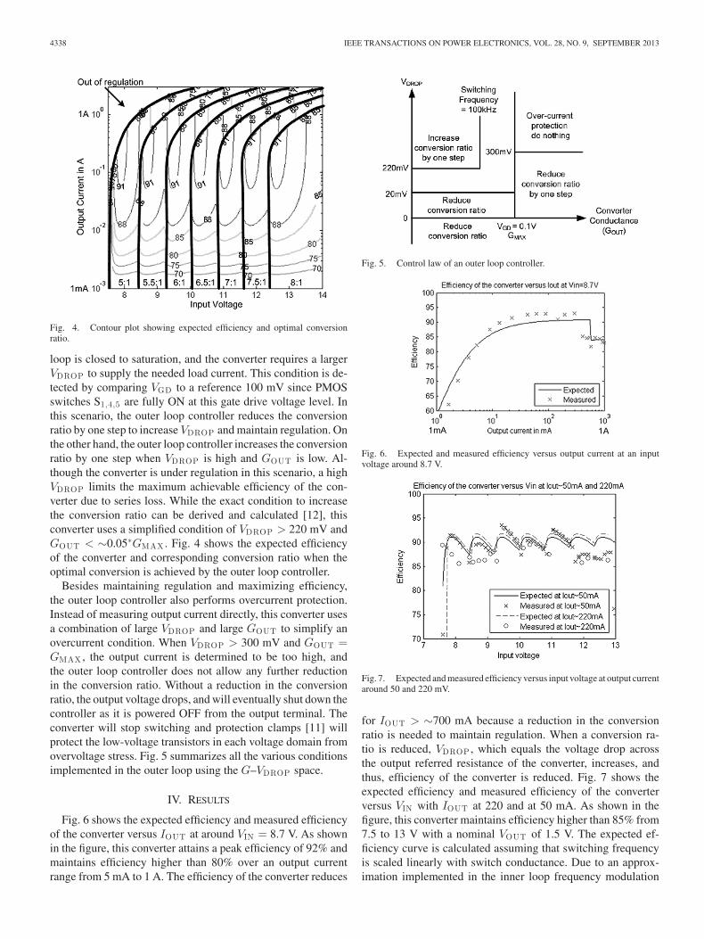
Fig. 4. Contour plot showing expected efficiency and optimal conversionratio.
loop is closed to saturation, and the converter requires a largerVDROP to supply the needed load current. This condition is de-tected by comparing VGD to a reference 100 mV since PMOSswitches S1,4,5 are fully ON at this gate drive voltage level. Inthis scenario, the outer loop controller reduces the conversionratio by one step to increase VDROP and maintain regulation. Onthe other hand, the outer loop controller increases the conversionratio by one step when VDROP is high and GOUT is low. Al-though the converter is under regulation in this scenario, a highVDROP limits the maximum achievable efficiency of the con-verter due to series loss. While the exact condition to increasethe conversion ratio can be derived and calculated [12], thisconverter uses a simplified condition of VDROP > 220 mV andGOUT < ∼0.05∗GMAX . Fig. 4 shows the expected efficiencyof the converter and corresponding conversion ratio when theoptimal conversion is achieved by the outer loop controller.
Besides maintaining regulation and maximizing efficiency,the outer loop controller also performs overcurrent protection.Instead of measuring output current directly, this converter usesa combination of large VDROP and large GOUT to simplify anovercurrent condition. When VDROP > 300 mV and GOUT =GMAX , the output current is determined to be too high, andthe outer loop controller does not allow any further reductionin the conversion ratio. Without a reduction in the conversionratio, the output voltage drops, and will eventually shut down thecontroller as it is powered OFF from the output terminal. Theconverter will stop switching and protection clamps [11] willprotect the low-voltage transistors in each voltage domain fromovervoltage stress. Fig. 5 summarizes all the various conditionsimplemented in the outer loop using the G–VDROP space.
IV. RESULTS
Fig. 6 shows the expected efficiency and measured efficiencyof the converter versus IOUT at around VIN = 8.7 V. As shownin the figure, this converter attains a peak efficiency of 92% andmaintains efficiency higher than 80% over an output currentrange from 5 mA to 1 A. The efficiency of the converter reduces
Fig. 5. Control law of an outer loop controller.
Fig. 6. Expected and measured efficiency versus output current at an inputvoltage around 8.7 V.
Fig. 7. Expected and measured efficiency versus input voltage at output currentaround 50 and 220 mV.
for IOUT > ∼700 mA because a reduction in the conversionratio is needed to maintain regulation. When a conversion ra-tio is reduced, VDROP , which equals the voltage drop acrossthe output referred resistance of the converter, increases, andthus, efficiency of the converter is reduced. Fig. 7 shows theexpected efficiency and measured efficiency of the converterversus VIN with IOUT at 220 and at 50 mA. As shown in thefigure, this converter maintains efficiency higher than 85% from7.5 to 13 V with a nominal VOUT of 1.5 V. The expected ef-ficiency curve is calculated assuming that switching frequencyis scaled linearly with switch conductance. Due to an approx-imation implemented in the inner loop frequency modulation
NG AND SANDERS: HIGH-EFFICIENCY WIDE-INPUT-VOLTAGE RANGE SWITCHED CAPACITOR POINT-OF-LOAD DC–DC CONVERTER 4339
Fig. 8. Oscilloscope plot of loading and unloading output current step of 1 Aat input voltage equals 9 V. Timebase 20 μs/div.
TABLE IICOMPONENTS USED AND CONTRIBUTION TO POWER LOSS
block, the converter may switch faster (reduces efficiency) orslower (increases efficiency) than the expected frequency. Fig. 8shows the load transient response of the converter during load-ing and unloading steps of 1 A. On the loading transient, afterfirst increasing switch conductances to their maximum values,the controller decreases the conversion ratio from 5.5 to 5, inorder to meet the load. On the unloading transient, the controllerimmediately stops clocking, and then adjusts the conversion ra-tio back to 5.5 to be prepared to continue operation. Clockingis only initiated when the stored charge in the output capacitoris reduced, and the output recovers to its regulated value. Theoutput voltage is regulated to within 30 mV during the transient.
Table II shows the components used in this converter andthe contributing factors to power loss. Off-chip X5R EIA sizecode 0603 ceramic capacitors are used due to their high-densitycapacitance and low cost. A maximum switching frequency of2.5 MHz is chosen for this converter based on the approximateESR corner frequency of 5 MHz of these power train capacitors.The widths of the power train switches are chosen such thatthey contribute roughly half of the fast switching limit outputresistance, RFSL . In the asymptotic fast switching limit, the
Fig. 9. Die photo of the fabricated silicon chip.
Fig. 10. Comparison of efficiency between this work and similar works.
voltages on the power train capacitors remain constant, andcurrent flows are represented by square waveforms within eachphase of conduction. In this case, the output referred resistance isdetermined by the resistances—switch, metal, ESR, bond-wire,etc., [1]. In contrast, in the slow switching limit (SSL), the outputreferred resistance is determined by the values of the power-traincapacitors [1]. In the asymptotic SSL, capacitors are allowedto fully equilibrate after each clock edge, and consequently,output resistance is determined only by capacitor values in thislimit. Table II also shows the output referred resistance, ROUT ,at 2.5 MHz switching frequency, at which the circuit outputresistance is dominated by the fast switching limit impedance.As evidenced from Table II, power loss at 1 A load is dominatedby conduction loss of bond-wire and on-chip metal resistances,rather than conduction loss due to on-chip MOS channel orpower-switch gate-drive loss. Fig. 9 shows the die photo ofthe fabricated silicon in a 0.18-μm CMOS process. The totaldie area of this experimental converter is 11.55 mm2 , but only

4340 IEEE TRANSACTIONS ON POWER ELECTRONICS, VOL. 28, NO. 9, SEPTEMBER 2013
TABLE IIICOMPARISON BETWEEN THIS WORK AND SIMILAR WORKS
Fig. 11. Comparison between this work and similar works.
about 20% of the die area is occupied by active power traindevices. Rather, die area is dominated by bond pads and otherconservative design considerations for this experimental chip.Solder bump interconnect and a thick on-chip metal layer wouldallow a substantial performance improvement, manifested inreduced diesize.
Fig. 10 shows a graph comparing the peak efficiency of thisconverter with that of similarly rated converters. All the sur-veyed buck and SC converters achieve respectable efficiency,but show a general trend of reduced efficiency as conversionratio increases. This study shows a significant increase in effi-ciency when compared to similarly rated SC and buck convert-ers. Table III and Fig. 11 compare critical performance metricsof this work with other existing technologies. In addition tohigher peak efficiency, the reported device achieves high effi-ciency for a wider range of load currents than in other com-petitive designs. Peak-to-peak output voltage transient duringa full-load current step is also respectable while using simi-lar values of input and output capacitances. Significantly, thisstudy also achieves an overall reduction in PCB area, passivecomponent height, and passive component cost when comparedto dc–dc converters with similar ratings. This comparison onlyconsiders input/output capacitors, inductors and power-train ca-pacitors because other auxiliary passives required for compen-sation, start-up, etc., are not fundamental and are eliminated orminimized in leading modern designs. The estimated cost ofcapacitors or inductors is based on large-volume purchase per-unit prices from Digikey. This study shows that the SC converterprovides a new direction for performance and cost advantageswith respect to the conventional buck converter.
V. CONCLUSION
The traditional inductor-based buck converter has been the de-fault design for switched-mode voltage regulators for decades.Switched capacitor (SC) dc–dc converters, on the other hand,have traditionally been used in low-power (<10 mW) and lowconversion ratio (<4:1) applications where neither regulationnor efficiency is critical. This study encompasses the completesuccessful design, fabrication, and test of a CMOS-based SCdc–dc converter, addressing the ubiquitous 12–1.5 V board-mounted point-of-load application. In particular, the circuit de-veloped in this study attains higher efficiency (92% peak, and>80% over a load range of 5 mA to 1 A) than surveyed compet-itive buck converters, while requiring less board area and lesscostly passive components. The topology and controller enablea wide input range of 7.5–13.5 V. Controls based on feedbackand feedforward provide tight regulation under worst case lineand load step conditions. This study shows that the SC convertercan outperform the buck converter, and thus, the scope of SCconverter application can and should be expanded.
ACKNOWLEDGMENT
The authors would like to thank National Semiconductor formanufacturing the test silicon.
REFERENCES
[1] M. Seeman and S. Sanders, “Analysis and optimization of switched-capacitor dc–dc converters,” IEEE Trans. Power Electron., vol. 23, no. 2,pp. 841–851, Mar. 2008.
[2] M. Seeman, V. Ng, H.-P. Le, M. John, E. Aton, and S. Sanders, “A compar-ative analysis of switched-capacitor and inductor-based dc–dc conversiontechnologies,” in Proc. IEEE Workshop Control Model. Power Electron.(COMPEL), Jun. 2010.
[3] M. Seeman, “A design methodology for switched-capacitor dc-dc con-verters,” Ph.D. dissertation, UC Berkeley, Berkeley, CA, May 2009.
[4] High Efficiency, 250 mA Step-Down Charge Pump, Texas Instruments(TPS60503), Dallas, TX, 2002.
[5] 500 mA High Efficiency, Low Noise, Inductor-Less Step-Down DC/DCConverter, Linear Technology (LTC3251), Milpitas, CA, 2003.
[6] 1A Simple Switcher Power Module With 20V Maximum Input Voltage,National Semiconductor Inc. (LMZ12001), Santa Clara, CA, Jun. 2010.
[7] 1.5A, 15V Monolithic Synchronous Step-Down Regulator, Linear Tech-nology (LTC3601), Milpitas, CA, 2009.
[8] 2A, 16V, Non-Synchronous Step-Down, DC/DC Regulator, Fairchild Semi-conductor Inc. (FAN8301), San Jose, CA, Nov. 2008.
[9] 4.5V to 18V Input, 2-A Synchronous Step-Down Swift Converter WithEco-Mode, Texas Instruments (TPS54226), Dallas, TX, Feb. 2011.
[10] J. F. Dickson, “On-chip high-voltage generation in nmos integrated cir-cuits using an improved voltage multiplier technique,” IEEE J. Solid-StateCircuits, vol. 11, no. 3, pp. 376–378, Jun. 1976.
[11] V. Ng, M. Seeman, and S. Sanders, “Minimum PCB footprint point-of-load dc–dc converter realized with switched capacitor architecture,” inProc. IEEE Energy Convers. Congr. Expo., Sep. 2009, pp. 1575–1581.

NG AND SANDERS: HIGH-EFFICIENCY WIDE-INPUT-VOLTAGE RANGE SWITCHED CAPACITOR POINT-OF-LOAD DC–DC CONVERTER 4341
[12] V. Ng, “Switched capacitor dc–dc converter: superior where the buckconverter has dominated,” Ph.D. dissertation, UC Berkeley, Berkeley,CA, Dec. 2011.
[13] L. Salem and R. Jain, “A novel control technique to eliminate output-voltage-ripple in switched-capacitor dc-dc converters,” in Proc. IEEE Int.Symp. Circuits Syst., Jun. 2011, pp. 825–828.
[14] V. Ng and S. Sanders, “A 92% efficiency wide-input voltage rangeswitched-capacitor dc-dc converter,” in Proc. IEEE Solid State CircuitConf., Feb. 2012, pp. 282–284.
Vincent W. Ng (M’10) received the B.S. degree inelectrical and computer engineering from CornellUniversity, Ithaca, NY, and the Ph.D. degree in elec-trical engineering from UC Berkeley, Berkeley, in2005 and 2011, respectively. His Ph.D. research wasfocused on designing switched-capacitor dc–dc con-verter for point-of-load applications.
Since 2010, he has been with Volterra Semicon-ductor, Fremont, CA, as a Design Engineer on voltageregulators in solar power application. His researchinterests include integrated circuits for power elec-
tronics, renewable energy, dc–dc conversion circuitries, and control systems.
Seth R. Sanders (F’10) received the S.B. degreesin electrical engineering and physics in 1981, andthe S.M. and Ph.D. degrees in electrical engineer-ing from the Massachusetts Institute of Technology,Cambridge, in 1985 and 1989, respectively.
Following an early experience as a Design En-gineer at the Honeywell Test Instruments Divisionin 1981–1983, he joined the UC Berkeley faculty in1989. He is a Professor of electrical engineering inthe Department of Electrical Engineering and Com-puter Sciences, University of California, Berkeley.
His research interests include high-frequency power conversion circuits andcomponents, design and control of electric machine systems, and nonlinear cir-cuit and system theory as related to the power electronics field. He is presently orhas recently been active in supervising research projects in the areas of flywheelenergy storage, novel electric machine design, renewable energy systems, anddigital pulse-width modulation strategies and associated IC designs for powerconversion applications. During the 1992–1993 academic year, he was on in-dustrial leave with National Semiconductor, Santa Clara, CA.
Dr. Sanders received the NSF Young Investigator Award in 1993 and multi-ple Best Paper Awards from the IEEE Power Electronics and the IEEE IndustryApplications Societies. He has served as the Chair of the IEEE Technical Com-mittee on Computers in Power Electronics, and as a Member-At-Large of theIEEE PELS Adcom.