atk 方法的扩展及其应用 王雪峰 苏州大学物理系 2009.11.28 zjnu-jinhua
TRANSCRIPT
ATK 方法的扩展及其应用
王雪峰
苏州大学物理系
2009.11.28 ZJNU-JinHua
Introduction
Inelastic scattering
Gate effect: electrostatic potential profile
Optimization of tridiagonal matrix inverter
Thermoelectric effect
Improvement of functionals
Summary
Outline
2009.11.28 ZJNU-JinHua

SIESTA TranSIESTAKS Hamiltonian Matrix
Nonequilibrium Green’s Function
TranSIESTA-C
ATK+VNL
Other transport packages:Smeagol, OpenMX,WanT,PWSCF
2009.11.28 ZJNU-JinHua
Jose M. Soler, et al., J. Phys.: CM 14, 2745 (2002); J. Taylor, H. Guo and J. Wang, Phys. Rev. B 63, 245407 (2001); M. Brandbyge, et al., Phys. Rev. B 65, 165401 (2002);www.openmx-square.orgwww.smeagol.tcd.iewww.icmab.es/siesta/www.quantumwise.comwww.wannier-transport.orgwww.pwscf.org

The systemT1, T2,
vibration
http://nanohub.org/
2009.11.28 ZJNU-JinHua

Band-diagram of the system in equilibrium

Effect of gate voltage
Not just a shift in reality!

Effect of source-drain voltage

Escape time, contact coupling

Current
N
E ( ) EI dED E I
Occupation number
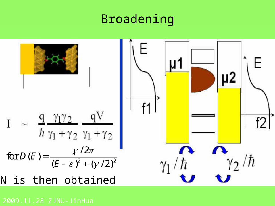
Broadening
2009.11.28 ZJNU-JinHua
2 2
/ 2for ( )
( ) ( / 2)D E
E
N is then obtained
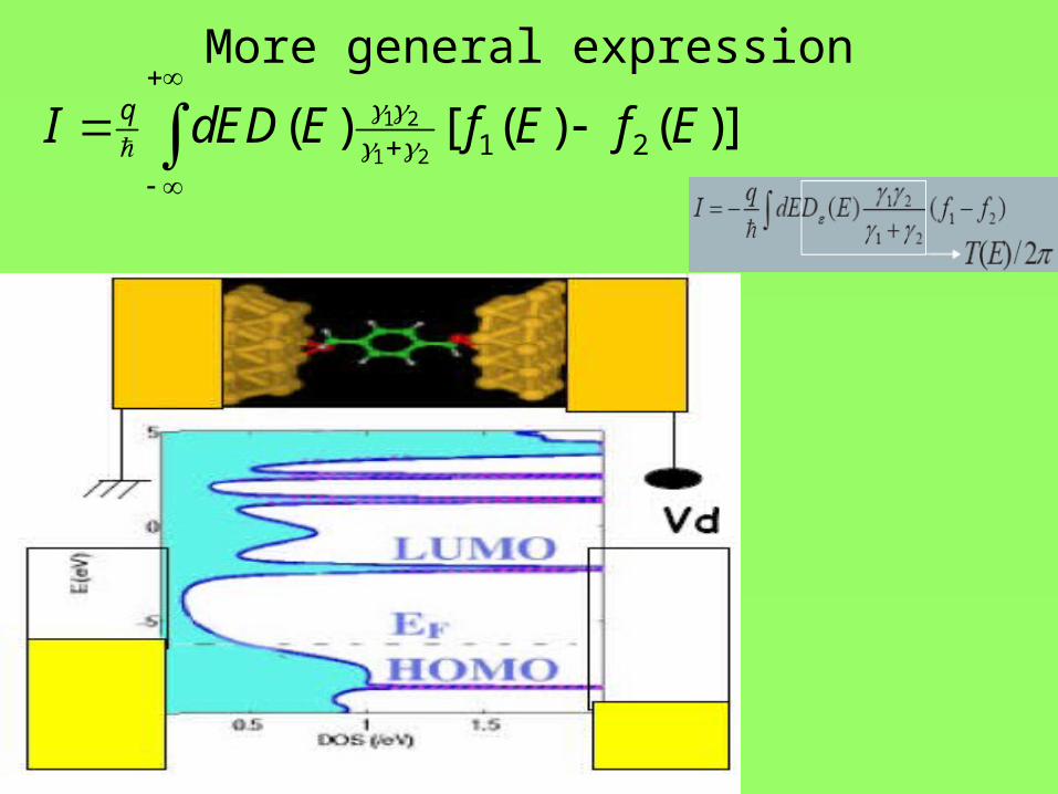
More general expression1 2
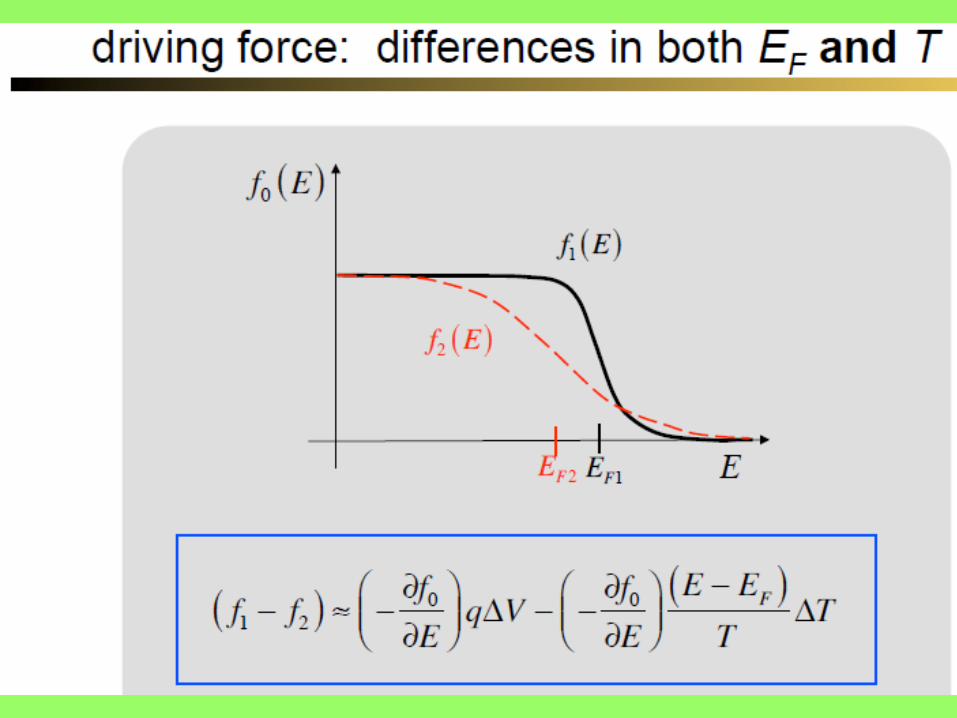
1 2 1 2( ) [ ( ) ( )]qI dED E f E f E

Potential profilecapacitance
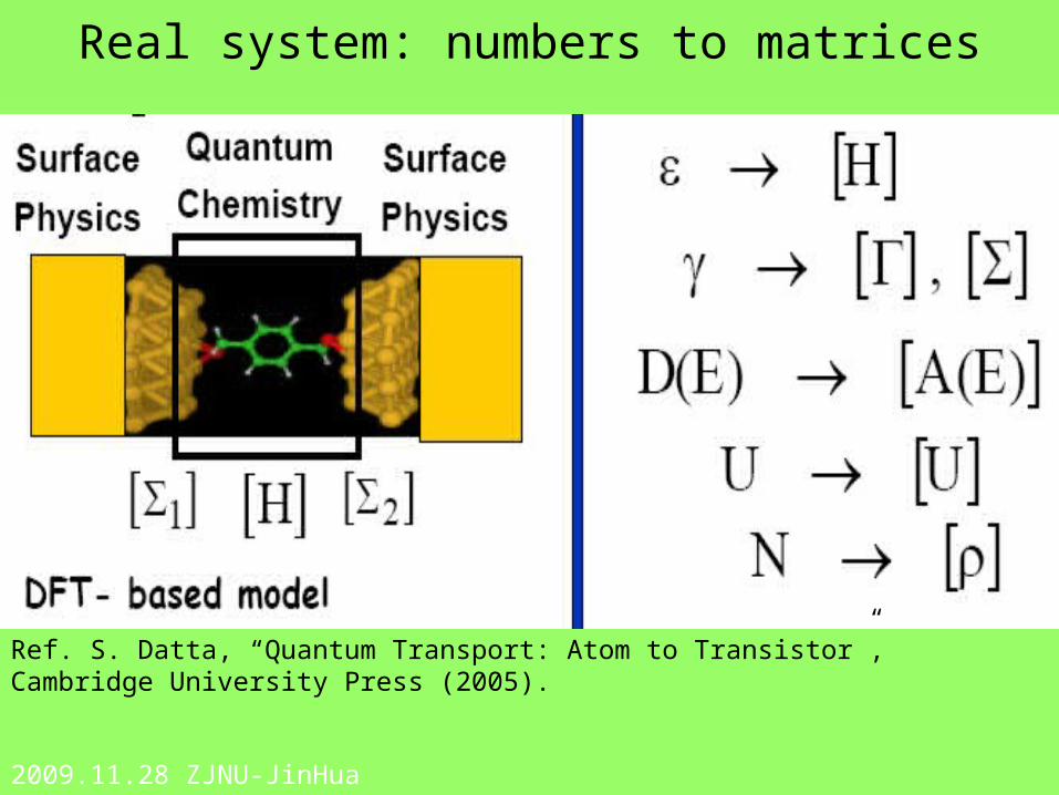
Real system: numbers to matrices
Ref. S. Datta, “Quantum Transport: Atom to Transistor”, Cambridge University Press (2005).
2009.11.28 ZJNU-JinHua
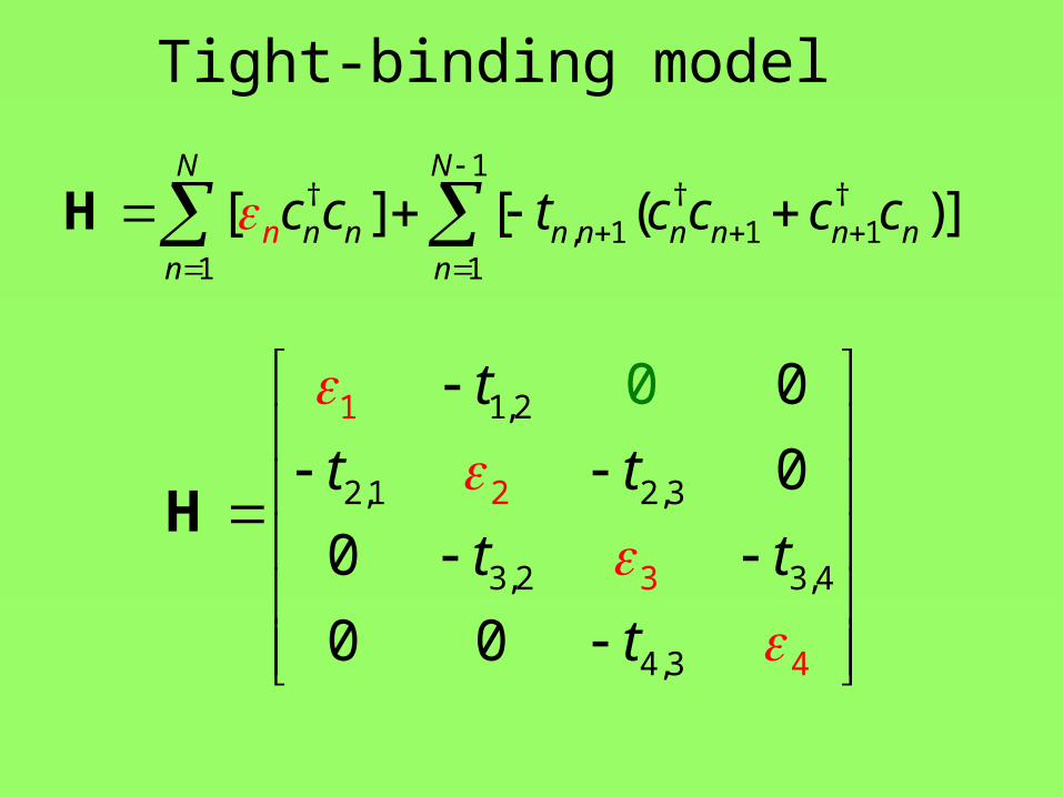
1† † †
, 1 1 11 1
[ ] [ ( )]N N
n n n n n n n nnn n
c c t c c c c
H
Tight-binding model
1,2
2,1 2,3
3,2 3,4
4
1
2
3
,3 4
0
0
0
0
0 0
t
t t
t t
t
H

Inflow and outflow
11 12
1 1
Trace[ ]
Tr[ ]
q in n
q in p out nh
I dE A G
dE G G
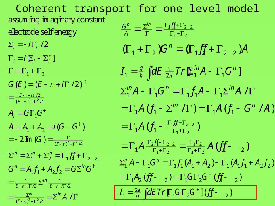
Coherent transport for one level model
2 2
2 2
1 2
1
/2( ) /4
1
†1 2
( ) /4
1 2 1 1 2 2
†1 1 2 2
assuming imaginary constant
electrode self energy
/ 2
[ ]
( ) ( / 2)
( )
2 Im( )
i i
i i i
E iE
i
E
in in in
n in
i
i
G E E i
A G G
A A A i G G
G
f f
G A f A f G G
2 2
1 1/2 /2
( ) /4/
in
inE i E i
in
EA
1 1 2 2
1 2
1 2 1 1 2 2( ) ( )
n in f fGA
nG f f A
1 1 2 2
1 2
2 1 2 2 1 2
1 2 1 2
11 1 12
1 1 1 1 1
1 1 1 1
1 1
1 1 2
[ ]
/
( / ) ( / )
( )
( )
q in n
in n in
in n
f f
f f
I dE Tr A G
A G f A A
A f A f G A
A f
A A f f
1 1 1 1 1 2 1 1 1 2 2
1 2 1 2 1 2 1 2
21 1 2 1 2
( ) ( )
( ) G G ( )
[ G G ]( )
in n
eh
A G f A A A f A f
A f f f f
I dETr f f
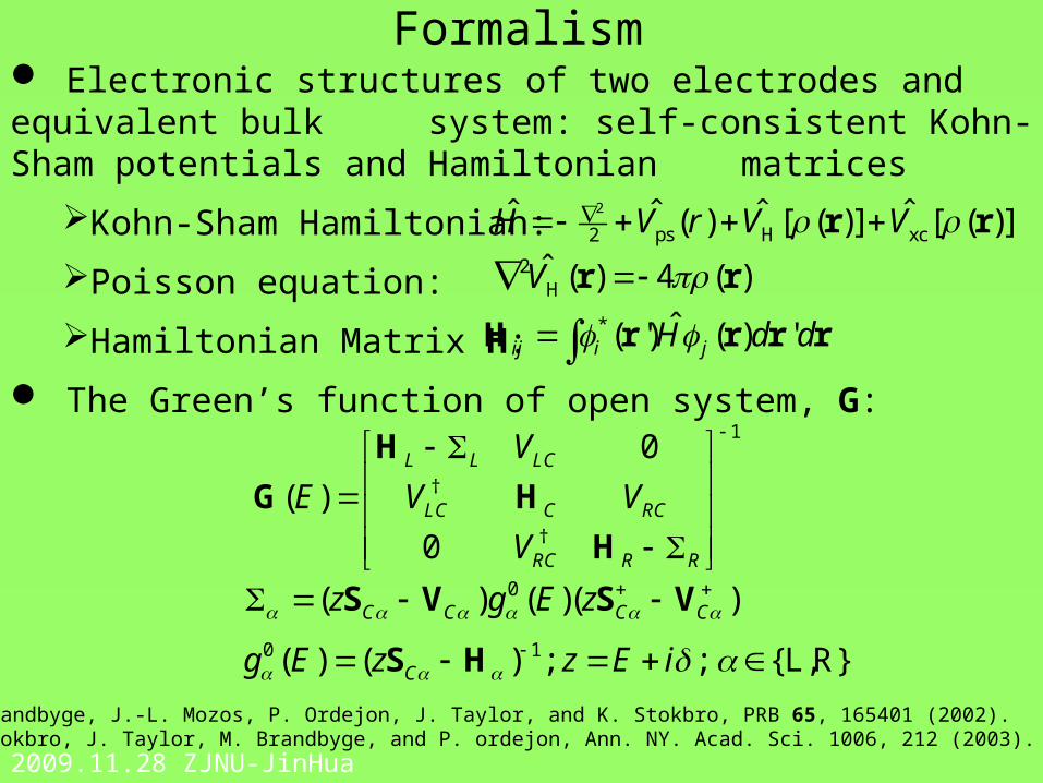
Electronic structures of two electrodes and equivalent bulk system: self-consistent Kohn-Sham potentials and Hamiltonian matrices
Kohn-Sham Hamiltonian:
Poisson equation:
Hamiltonian Matrix H:
The Green’s function of open system, G:
Formalism
2
ps H xc2ˆ ˆ ˆ ˆ( ) [ ( )] [ ( )]H V r V V r r
2H ( ) 4 ( )V r r
* ˆ( ') ( ) 'ij i jH d d H r r r r
1
†
†
0
( )
0
L L LC
LC C RC
RC R R
V
E V V
V
H
G H
H0( ) ( )( )C C C Cz g E z
S V S V0 1( ) ( ) ; ; {L,R}Cg E z z E i S H
M. Brandbyge, J.-L. Mozos, P. Ordejon, J. Taylor, and K. Stokbro, PRB 65, 165401 (2002).K. Stokbro, J. Taylor, M. Brandbyge, and P. ordejon, Ann. NY. Acad. Sci. 1006, 212 (2003).
2009.11.28 ZJNU-JinHua
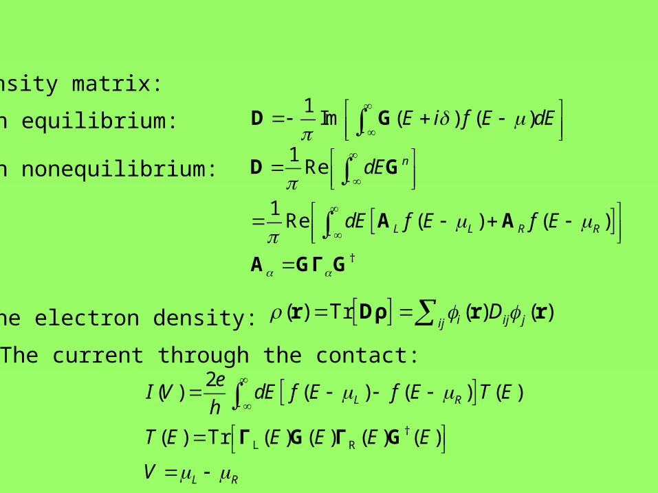
Density matrix:
In equilibrium:
In nonequilibrium:
The electron density:
The current through the contact:
1Im ( ) ( )E i f E dE
D G
†
1Re
1Re ( ) ( )
n
L L R R
dE
dE f E f E
D G
A A
A GΓ G
( ) Tr ( ) ( )i ij jijD r Dρ r r
†
L R
2( ) ( ) ( ) ( )
( ) Tr ( ) ( ) ( ) ( )
L R
L R
eI V dE f E f E T E
h
T E E E E E
V
Γ G Γ G
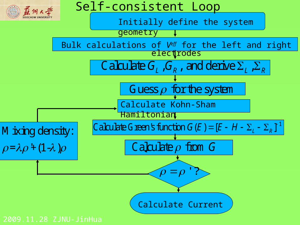
Calculate Kohn-Sham Hamiltonian
Calculate , , and derive ,L R L RG G
Guess for the system
1Calculate Green's function ( ) [ ]L RG E E H
Initially define the system geometry
Bulk calculations of Veff for the left and right electrodes
Calculate from G
' ?
Calculate Current
Mixing density:
= '+(1- )
Self-consistent Loop
2009.11.28 ZJNU-JinHua
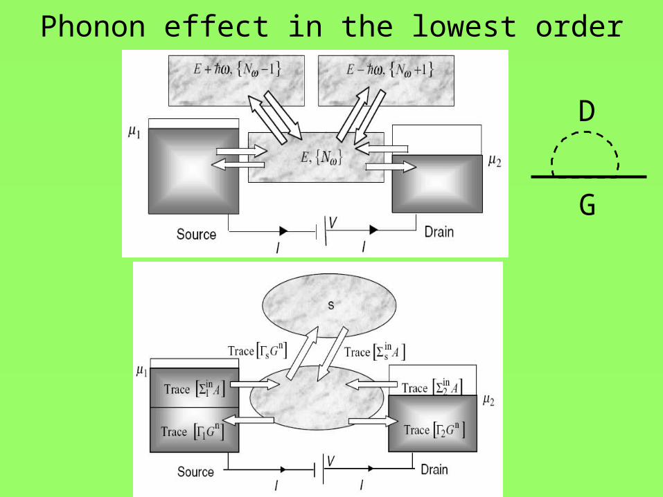
Phonon effect in the lowest order
D
G

Inelastic scattering
p.287
p.336

Elastic scattering for one level model
2 2
2 2
2 2
1 2 0
1
/2( ) /4
†
( ) /4
1 1 2 2 0
† 1 1/2 /2
( ) /4
( ) ( / 2)
( ) 2 Im( )
/in
E iE
E
in n
n in inE i E i
in
E
D A
G E E i
A i G G G
f f D G
G G G
A
1 1 2 2 0
1 2 0
1 1 2 2
1 2
0 1 2
1 1 2 2 0
1 2 1 1 2 2
( )
( )
( ) ( )
nn in
n
f f D GGA D A
n n
n
n
f fGA
D AG G
f f A D G A
G f f A
1 1 2 2
1 2
2 1 2 2 1 2
1 2 1 2
12
0 0
11 1 12
1 1 1 1 1
1 1 1 1
1 1
1 1 2
[ ]
0
0
[ ]
/
( / ) ( / )
( )
( )
q in ns s s
in n n ns s
s
q in n
in n in
in n
f f
f f
I dE Tr A G
A G D AG D G A
I
I dE Tr A G
A G f A A
A f A f G A
A f
A A f f
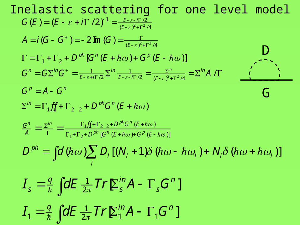
Inelastic scattering for one level model2 2
2 2
2 2
1 / 2( ) / 4
( ) / 4
1 2
1 1/ 2 / 2 ( ) / 4
1 1 2 2
( ) ( / 2)
( ) 2 Im( )
[ ( ) ( )]
/
( )
in
E iE
E
ph n p
n in in inE i E i E
p n
in ph n
G E E i
A i G G G
D G E G E
G G G A
G A G
f f D G E
1 1 2 2
1 2
( )
[ ( ) ( )]
( ) [( 1) ( ) ( )]
ph nn in
ph n p
f f D G EGA D G E G E
phi i i i i
i
D d D N N
12
11 1 12
[ ]
[ ]
q in ns s s
q in n
I dE Tr A G
I dE Tr A G
D
G

A7-atom gold wire with L=29.20 Å is coupled to semi-infinite electrodes. The vibrational region is taken to include the atoms in the pyramidal bases. The device region (describing the e-ph couplings) includes also the outermost surface layers.
T. Frederiksen, M. Paulsson, M. Brandbyge, A. P. Jauho, Phys. Rev. B 75, 205413 (2007)2009.11.28 ZJNU-JinHua

The measured (noisy black curves) are for different strain. The calculated (smooth colored lines) are for different damping.
T=4.2K

Gate effect: Si MOSFET devices
Equivalent capacitive circuit
Vg
MOSFETs are the most important building blocks Si nanostructures are still the fundamental units: Si cluster, nanowire, nanoslab, and so on
2009.11.28 ZJNU-JinHua

Top-down technologiesin traditional semiconductor industry --
Microelectronicsm 100nm 10nm nm 0.1nm
45 32 0.54Si latticeCPU wireITRS
Intl. Tech. Roadmap Semi.
Bottom-up technologiesMolecular electronics, Spintronics, Quantum computation
m0.1nm nm 10 nm 100nm
DNA
Si latticeH2O
Quantum dot
nanotube, nanowire
2009.11.28 ZJNU-JinHua
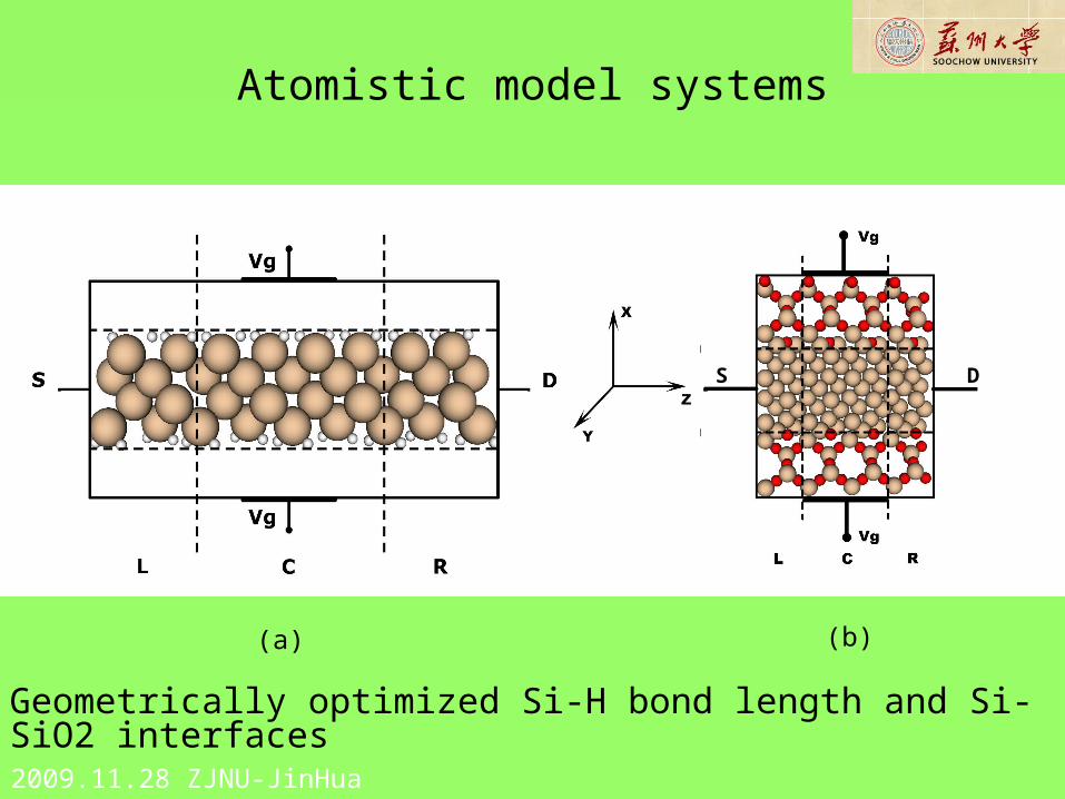
S D
(a) (b)
Atomistic model systems
Geometrically optimized Si-H bond length and Si-SiO2 interfaces
2009.11.28 ZJNU-JinHua
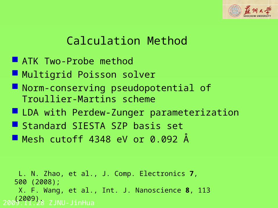
ATK Two-Probe method Multigrid Poisson solver Norm-conserving pseudopotential of Troullier-
Martins scheme LDA with Perdew-Zunger parameterization Standard SIESTA SZP basis set Mesh cutoff 4348 eV or 0.092 Å
Calculation Method
2009.11.28 ZJNU-JinHua
L. N. Zhao, et al., J. Comp. Electronics 7, 500 (2008); X. F. Wang, et al., Int. J. Nanoscience 8, 113 (2009).

Si-slab based MOSFET capacitor
Result:
2009.11.28 ZJNU-JinHua

Charge and electrostatic potential distribution
X
V
X
2009.11.28 ZJNU-JinHua

Total induced charge and surface potential versus gate voltage
Q Vs
Vs
Vg Vg Vg
Q
2009.11.28 ZJNU-JinHua

Transmission spectrum under gate voltageT
T
2009.11.28 ZJNU-JinHua

Thermoelectric effects

Thermoelectric effects

thermoelectric devices
Thermal conductance
2009.11.28 ZJNU-JinHua

2009.11.28 ZJNU-JinHua

2009.11.28 ZJNU-JinHua

1 1 1 2 2 2
1 1 1 2 2 2
( ) ( )[ ( , , ) ( , , )]
( ) ( )[ ( , , ) ( , , )]
qh
qQ h
I dED E T E f E T f E T
I dED E ET E f E T f E T
Charge current and heat current
2 1
2 1
0,I
VS
T T T
Q
I G V SG T
I TSG V K T
Here we do not include the phonon effect
2009.11.28 ZJNU-JinHua

silicon nanowiresA. I. Hochbaum et al., Nature 451, 163 (2008).
silicon nanowires array
Akram I. Boukai, ibid. 451, 168 (2008).
ZT=S2T/

ATK method is under development Optimize algorithm: faster, better
accuracy, larger system Inelastic scattering Multi-terminal systems: transistor Temperature bias: thermoelectric
effect Better density functional
Summary
2009.11.28 ZJNU-JinHua
