cdteピクセル検出器...
TRANSCRIPT

CdTeピクセル検出器とその周辺技術
高橋忠幸
JAXA 宇宙科学研究本部(ISAS)

ガンマ線イメージャー
キロ電子ボルト メガ電子ボルト
ガンマ線で細かな内部構造を探る~数百ミクロン
ガンマ線望遠鏡
医療用非破壊検査放射性廃棄物検査放射性物質探索(テロ対策)(Homeland Security, US)天体観測
ガンマ線で遠方のガンマ線を探る(数mm/数cm)
角度分解能
ACRORAD提供
ピクセルサイズは、用途に応じて100ミクロンから数mmまで
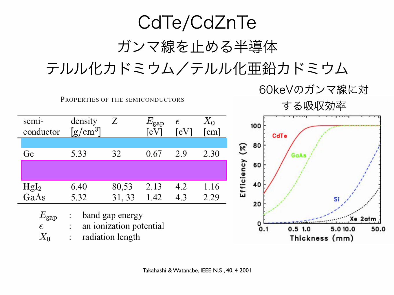
CdTe/CdZnTeガンマ線を止める半導体
テルル化カドミウム/テルル化亜鉛カドミウム60keVのガンマ線に対
する吸収効率
Takahashi & Watanabe, IEEE N.S , 40, 4 2001

CdTe/CdZnTe半導体
CdTe single crystal (ACRORAD)
5 cm
● p型にもn型にもなる● THM-CdTe (ACRORAD)では5cm角の単結晶Wafer可能(一様性、再現性がよい)(p型)● HPB-CdZnTe (eV-Products)では大きなインゴットが得られるが1cm角以上の大きさの単結晶は難しい(比抵抗は高いが、一様性が悪い)(n型)● 用途に応じた使い分けが必要
表面電極をつける技術も大切電極素材(Pt、Auなど)
前処理、後処理
ピクセル電極の例 100ミクロン
高橋、中澤物理学会誌2005年1月

CdTe Imager
50mm
アクロラド提供
有効視野 50x50 mm空間分解能 0.1 mmフレーム 50 fr/秒
ただしスペクトル情報はないこれのカラー版が求められている

Takahashi et al. NIM A 2005 Tanaka et al. 2003
CdTe Diode(20 deg)
高いエネルギー分解能を持つCdTeダイオード検出器の開発
(宇宙研/ACRORAD)
CdTe Diode(-40 deg.)
● 薄型(0.3-1.0 mm)● ショットキーダイオード (In/CdTe/Pt)● ガードリング
● 低いリーク電流● 高いバイアス電圧
● 完全電荷収集● 安定性
Amptek:ガンマ線プローブ等に採用
Δ[email protected] keV

現在進めているプロジェクト(www.astro.isas.jaxa.jp/~takahasi)
• すざく衛星による宇宙X線、ガンマ線観測(硬X線検出器 - HXD -の開発:1993年から)
• 将来のX線・ガンマ線衛星のための検出器開発
• 高いエネルギー分解能を持つ硬X線検出器とイメージャー
• CdTe/CdZnTeを用いたピクセル検出器• シリコンストリップ検出器 (with 田島@SLAC, with 深沢@広大)
• ガンマ線イメージャー(Si/CdTe半導体コンプトンカメラ)
• 組み込み型データ処理装置(with 能町@阪大)
• アナログLSI開発(with 田島@SLAC, with 池田@ISAS)
Suzaku July.10th 2005
産学連携プロジェクト(国内、合衆国、ヨーロッパへ技術移転)
CdTeガンマ線モジュール医療、検査・探査装置
HXDone unit

CdTeピクセル検出器今、NeXTをめざして私たちが開発しているもの
(ピクセルサイズ 250-500 ミクロン角)硬X線撮像検出器 (HXI) 軟γ線撮像検出器 (SGD)
2cm x 2cm から 3cm x 3cmの大きさのCdTe イメージャー
(ピクセルサイズ 1.5-2.0 mm)
シリコン両面検出器
Si/CdTe Compton Camera
宇宙は要求仕様が高い上、壊れてはいけないので、最初から筋のよいやり方をしないといけない
Takahashi et al. 2004

CdTeピクセル検出器今、異分野から我々のチームが技術協力を求められているもの
Homeland Securityの観点から、新しい検出器が求められている(核物質、放射性物質の違法所持、搬入の阻止)。 条件は:High Z, High Density, High Energy Resolution
求む:これまでにない、性能の検出器を (Department of Homeland Security, USA IEEE NS 2005基調講演から)
・150 keV程度まで、エネルギー分解能2keV以下、ピクセル分解能1.4 mm
・511 keVで、1%のエネルギー分解能、高効率、位置分解能は1-2 mm
海外では
ENERGY-RESOLVED COHERENT SCATTER CT GEOMETRY
In Figure 2 the geometry of Coherent Scatter CT (CSCT) data acquisition is shown. A fan-beam illuminates the object
and the transmitted fan reaches the transmission CT detector at its central row. The transmission data can be used for
attenuation correction and also for generating a conventional CT image. Off-center rows of the detector receive solely
scattered radiation and form a 2-dimensional data set for each projection.
In contrast to the conventional fan-beam CSCT setup25
now a separate energy-resolving detector is applied (marked as
‘CSCT-detector’ in Figure 2). This can be a multi-line detector to realize higher throughput, but for a proof-of-principle
it is sufficient that the energy-resolving detector consists of only one row. Looking at Eq. (4) is becomes clear that a
range of momentum transfers can be measured with a single detector line (which means that the scatter angle ! is
roughly constant (see Figure 3)), when energy discrimination is used.
Since scattering changes the direction of the radiation, a fan-beam CSCT setup requires collimator lamellas in front of
the scatter detector to ensure spatial resolution.
Figure 2: Geometry of fan-beam Coherent Scatter CT. A fan-beam is used to illuminate one object slice. The central detector row
receives the transmitted radiation while the out-of-center rows receive only scattered radiation. In energy-resolved CSCT an extra
detector (‘CSCT-detector’) is applied which measures the energy of each incoming photon. A 1-D collimator in front of the detector is
required for spatial resolution of the setup.
Even with the lamellas in place each detector element receives radiation scattered along a certain path through the object.
This is depicted in Figure 3. In the confined geometry of a CT-scanner the distance between the object and the detector
will be of the same order of magnitude as the sample size. Therefore, a detector pixel picks up radiation that not only
originated from an elongated path through the object but was also scattered under various scatter angles. This is shown as
the gray-shaded region in Figure 3.
However, the relationship between the position within the object and the momentum-transfer parameter x can be
calculated if the energy of the measured photon is known. Using Eq. (4) for small angles this gives
d
a
hc
Ex
2"# . (5)
For one detector row, a (the distance of the detector pixel from the transmitted beam) will be constant and x will only
vary with d, where d describes the distance from an object voxel to the detector.
The dependence of x on the position within an object is shown in Figure 4. The rectangle drawn in the figure indicates
that for an object with a diameter of 20 cm and a usable energy spectrum ranging from 30 keV to 160 keV, a complete
dataset can be collected for x # 1.3 nm-1
... 4.8 nm-1
. The geometry parameters are given in the figure caption.
医療
with 原子力機構&群馬大学
with 某海外メーカ
Energy Resolved Coherent Scatter CT

Alternative Detector substrates • Si • Diamond • GaAs
「核」となる検出器
1. ガンマ線を止める半導体 (高品質のウェハー)2. 半導体ピクセル化技術3. 読み出し用アナログLSI
4. 実装技術 a) バンプ接合 b) フリップチップ技術5. 読み出し、DAQ、RTOS
6. 大面積化 a) 大面積CdTeウェハー b) バッタブルの技術 c)大型ASIC、
ハイブリッドピクセル検出器必要となる技術
pixel readout chip
semiconductor pixel detector
pixel contact
flip chip bonding

低雑音アナログVLSI
1)ひとつひとつのフォトンを検出し、カウンタで数えて イメージにする2)ひとつひとつのフォトンを検出し、リストモードで送り出し、 詳細なスペクトルと同時にイメージを作る
● 高い感度(一つ一つのX線光子、ガンマ線光子の検出を可能にする) ● エネルギー情報を使えるので、ディスクリがかけられる ● あるエネルギー範囲のみのイメージ、またカラー写真がとれる ● ピクセルあたりのカウントレートは整形時定数によって制限される (τ=1 microsec -> ~100 kcnts/s/pixelが最大)
フォトンカウンティング型

主なASICのアーキテクチャ1. Fast-Shaper/Slow Shaper
Level-sensitive
Discriminator
Semigaussian“fast” shaper
Monostable(fixed width)
Semigaussian“slow” shaper
ChargeIntegrator(preamp.)
S/H Vss
Vdd
TriggerOut
TAVA
Multiplexer
analog out
2. Capacitor Array
VA/TA (IDEAS,宇宙研)Medpix2 (Cern)H02 (宇宙研)
Caltech
3. TOTHXI chip(LBL/宇宙研)LBLと宇宙研の共同開発
Time Over Thresholdの(ATLASの低雑音化)(TOTで100 e- は Challenging
結局、殆ど0から開発)
低電圧で、ダイナミックを稼げる16x16完成、試験中

2mm
2dim version(200µm pitch)
32x32 (蛭田講演)
12x12
VLSI based on deep submicron CMOSTechnology
(a) Low Noise (ENC ~50 e- RMS at 0pF)
(b) Low Power (~0.2 mW/pixel) (c) Self Trigger Capability (d) Low Rate
読み出し用アナログASIC の開発
2000- IDEASと2000- Bonn U.と2003- LBNLと2003 - Caltechと
1. 低雑音化2. 低消費電力3. ピクセルへの対応
with IDEAS
共同研究
VDECにて
2002- KEK(池田)と
2003-2004 経産省 Project2004- JAXA Project
16x16
GEMの読み出しには電極を大きくするだけ

Development for the Next Prototype: VA64TA
7 mm
VA64TA: 64 channel analog ASIC By ISAS, SLAC & Ideas ASA, Norway
Measured Power Consumption: 0.4 mW/chOne order lower than VA32TA
Expected Noise: (rms)Majority selector circuit for the tolerance against
SEU
2005
Energy resolution: 1.1 keV @ 60 keV 1.2 keV @ 122 keV
Same as VA32TA
Energy threshold: ~ 4.0 keV
Si Stripによるスペクトル
Tajima et al. 2003, Tanaka et al. 2005

アナログLSIオープンIPプロジェクト @ ISAS/JAXA
K01
H01 H02
T01
T02
K02
T01B
0.35 umROHM
0.35 umROHM
0.35 umROHM
0.35 umROHM
0.35 umTSMC
0.25 umTSMC
マスクエラー
層間ショート
4096 ch200 umpixel
64 ch
64 ch
256 ch280 um
32 ch
0.35 umTSMC
144 ch260 um
波高分析型2次元アレー
計数型2次元アレー
計数型1次元アレー
波高分析型1次元アレー
小林修論
井上修論
井上修論
田村修論
蛭田修論
池田&高橋
2002
2003
2004
2005
Tamura et al. 2005Ikeda et al. 2006, Hiruta et al. 2006

H02チップのレイアウト64 x 64 (15mm角)TSMC/0.25ミクロン5層メタル配線deep N-well
1ピクセルのレイアウト(200ミクロン角)

Bump Bondingシリコンチップ用
(Waferを相手にしたプロセスであることが多く使いにくい)
(CdTeには、うまく適応できなかった:熱、圧力)
X-ray/Gamma-ray
Electrode
CdTe/CdZnTe
ASIC
Support board

CdTeのために開発したIn/Au Stud• In/Au スタッドバンプ(背の高いバンプ)ー>入力容量をさげる• CdTe/CZT に適している(低温、ソフト)
これが我々にとって一番の鍵の技術となった。ISAS&MHI US特許、ヨーロッパ、日本特許申請中(Takahashi et al. IEEE NS. 2001)
CdTe
ASIC
underfill
50 micron
宇宙研&三菱重工業名古屋誘導システム(民生の最先端実装技術、MEMS、ナノテク
LSI パッケージング、宇宙応用)
ボンディング
ボンディングヘッド
加熱・圧力(PC制御)
日本の実装マシンは世界一(九州松下、澁谷工業他)

例:カウンティング素子を用いたCdTeイメージャー
宇宙研/ボン大学共同プロジェクト(フォトカウントChip)
200μm角というような細かなピクセル検出器の実証を世界に先駆けて行った (2001)
12.8mm

例:500μmピッチ大面積CdTeピクセル検出器
2.5cm
1.3cm
pixel size: 580 µm x 580 µmhybrid size : 1.3 cm x 2.5 cmpower : 50 µW/pixel
CdTe (Pt/CdTe/Pt) & バンプ接合 (ISAS,ACRORAD,MHI)VLSIとDAQ (Caltech)
0.4mm thick
Oonuki et al. SPIE 2004

CdTeガンマ線モジュール
Takahashi et al. 2006

area: 18 x 18 mm2, thickness: 0.5 mmpixel size: 2 x 2 mm2, 64ch, cathode sideguard ring : 1 mm widthbacking : 200 micron thick Al2O3
8x8 CdTe Pixel “Gamma-ray Module”64ch sum-spectrum
800 V
area: 11.2 x 11.2 mm2, thickness: 0.75 mmpixel size: 1.35 x 1.35 mm2, 64 ch
1400 V57Co 5 ºC122 keV FWHM 1.7 keV
New ASIC (VA32TA/VA64TA) by ISAS/SLAC/IDEAS

Spectra from 64 pixels
1.4 mm pitch 0.5 mm thick
module at 600 V
57Co 5 ºC 122 keV Av. FWHM 1.5 keVHigh Uniformity, NO-TAIL, High-ΔE
0 20 40 60 80 100 120 1400
200
400
600
800
1000
1200
1400
1600
1800
2000
2200

大面積化
4.4 cm x 1.1 cm1.4 mm Pitch
疑似バッタブルでしきつめた円筒型
CdTe検出器
米、ヨーロッパのメーカーに技術移転

半導体イメージング素子の応用
Si/CdTeコンプトンカメラ
Si(Z小) →散乱体 CdTe(Z大)→吸収体
半導体のみで構成↓
・優れたエネルギー分解能・優れた位置(角度)分解能・コンパクトな設計が可能
Si/CdTeの組合せ↓
・100keV~MeVで高効率・ドップラーの影響小
Takahashi et al. 2002, 2004, 2005, Mitani et al. 2004, Tajima et al. 2004, Tanaka et al. 2004, 2005, Watanabe et al. 2005, 2006

37.5
cm
RI source
γ
CdTe
18 mm -800 -600 -400 -200 0 200 400 600 800-800
-600
-400
-200
0
200
400
600
800
0
0.1
0.2
0.3
0.4
0.5
0.6
0.7
Reconstructed Image
22Na: 511 keV +/– 10 keV
radius 10°
x [mm]
y [m
m]
Prototype (1) - CdTe Compton -
0.5 mm thickTanaka et al. 2005

Spectrum Reconstruction
-800 -600 -400 -200 0 200 400 600 800-800
-600
-400
-200
0
200
400
600
800
0
0.1
0.2
0.3
0.4
0.5
0.6
Reconstructed Image
511 keV image
FWHM:7.3 keV@ 511 keV
Oonuki et al. 2005

Prototype (2) - Si / CdTe --
• Si (Z=14) is much suitable as a scatterer.
• CdTe (Z=48,52) works better as an absorber
Si 6 layers
3 CdTe pixels
26 mm
5 cm

コンプトン再構成(イメージ)
線源
DSSD
CdTe
40cm
γ
81keV ~ 662keV でのコンプトン撮像に成功
133Ba 81keV57Co 122keV133Ba 276~384keV22Na 511keV137Cs 662keV
理論限界(ドップラー限界)に近い分解能をはじめて実現
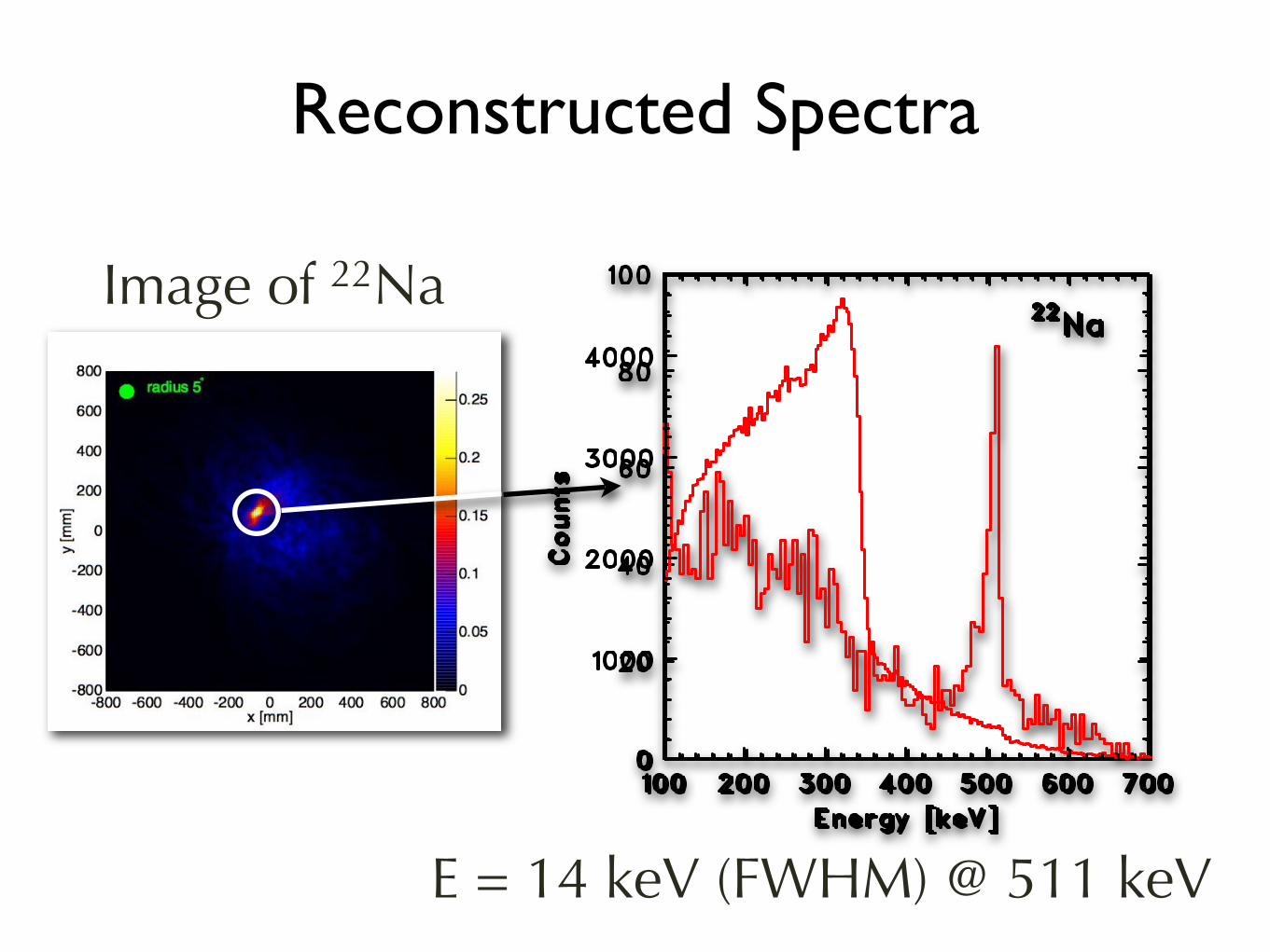
Reconstructed Spectra
Image of 22Na
E = 14 keV (FWHM) @ 511 keV

まとめ1. ガンマ線を止める半導体 (高品質のウェハー)2. 半導体ピクセル化技術3. 読み出し用アナログLSI
4. 実装技術 a) バンプ接合 b) フリップチップ技術5. 読み出し、DAQ、RTOS
6. 大面積化 (20cm角、30cm角) a)大面積CdTeウェハー b)バッタブルの技術 c)大型ASIC
@ISAS
ピクセル検出器の技術開発を進めている「民」の技術を使わないと、発展しない (大量生産を行なう事を最初から考える)「民」のニーズを知って、共同開発をすることが必要。(民にとって魅力的なビジネスモデルを提示する)
長期的な視野にたった開発が必要(特にASIC)
一人ではできない。
宇宙オープンラボ(JAXA産学官連携部)
蒸着装置
必須 必須

2006/01/26 12:53 PMSNIC06: Welcome
ページ 1/2http://www-conf.slac.stanford.edu/snic/default.htm
April 3 - 6, 2006Stanford Linear
Accelerator CenterStanford, California
in Particle, Astroparticle and Synchrotron Radiation
Home | Program | Committees | Request Invitation | Registration/Abstract | Participants | Visa |
Payment Options | Accommodations | Transportation | Tourism | Author Instructions |
First Announcement
The International Symposium on the Development of Detectors for Particle, Astroparticle and
Synchrotron Radiation Experiments is scheduled to take place at the Stanford Linear
Accelerator Center (SLAC), April 3 - 6, 2006. This will be the ninth conference in a series
that was started in 1977 jointly by experimenters at the SLAC and the Budker Institute for
Nuclear Physics at Novosibirsk. These conferences initially focused on detectors for e+ e-
colliding beam facilities, but more recently the focus has been enlarged to include
instrumentation for proton colliders.
In recognition of the fact that the research program at many High Energy Physics laboratories
is going to change dramatically in the years to come, the program for this Symposium will
cover detector development for experiments in three different areas of research: Particle
Physics, Astroparticle Physics, as well as experiments at Synchrotron Radiation Facilities. The
emphasis will be on detectors and sensors that are based on fundamentally similar concepts
and properties of matter. The goal of this Symposium is to bring together experts from these
different communities to exchange information and stimulate interdisciplinary developments.
The Symposium program will be organized in plenary sessions with invited speakers, and will
include longer overview talks and shorter oral presentations on specific applications or
developments. A poster session will supplement the shorter presentations. We plan to hold
sessions on
Single photon detectors
Silicon based detectors with high position or spectral resolution
Semiconductor developments
Imaging techniques
Detection of dark matter and cosmic microwave background
Instrumentation of particle and laser beams
High energy calorimeters
Charged particle identification devices
The attendance will be limited to 200 invited participants. If you are interested in attending
this Symposium, you can select here to request an invitation. Any questions about the
symposium may be directed to the Conference Committee at [email protected].
分野横断的検出器会議@SLAC
April 3-6, 2006
日本の技術の発信を
検出器の会議でもっと日本からの
招待講演が増えるようにならないといけない

Angular Resolution
θGeom ← Hit PositionsθComp ← E1, E2
θComp – θGeom 511 keV
src. position(known)
θGeom
ExperimentsSimulations
DopplerEnergyPosition
Si/CdTe Compton
CdTe-only Compton12 degree at 511 keV
(Doppler Limited)same situation for Ge