ch nh sn pb i perovskite solar cells covering up to graduate school of life science and systems...
TRANSCRIPT
CH3NH3SnxPb(1−x)I3 Perovskite Solar Cells Covering up to 1060 nmYuhei Ogomi,*,† Atsushi Morita,† Syota Tsukamoto,† Takahiro Saitho,† Naotaka Fujikawa,† Qing Shen,‡,∥
Taro Toyoda,‡,∥ Kenji Yoshino,§,∥ Shyam S. Pandey,† Tingli Ma,† and Shuzi Hayase*,†,∥
†Graduate School of Life Science and Systems Engineering, Kyushu Institute of Technology, 2-4 Hibikino, Wakamatsu-ku,Kitakyushu, Fukuoka 808-0196, Japan‡Graduate School of Informatics and Engineering, University of Electro-Communications, 1-5-1 Chofugaoka, Chofu, Tokyo182-8585, Japan§Department of Electrical and Electronic Engineering, University of Miyazaki, 1-1, Gakuen Kibanadai Nishi, Miyazaki 889-2192, Japan∥CREST, Japan Science and Technology Agency (JST), 4-1-8 Honcho Kawaguchi, Saitama 332-0012, Japan
*S Supporting Information
ABSTRACT: We report photovoltaic performances of all-solid state Sn/Pb halide-based perovskite solar cells. The cell has the following composition: F-doped SnO2layered glass/compact titania layer/porous titania layer/CH3NH3SnxPb(1−x)I3/regioregularpoly(3-hexylthiophene-2,5-diyl). Sn halide perovskite itself did not show photovoltaicproperties. Photovoltaic properties were observed when PbI2 was added in SnI2. The bestperformance was obtained by using CH3NH3Sn0.5Pb0.5I3 perovskite. 4.18% efficiency withopen circuit voltage 0.42 V, fill factor 0.50, and short circuit current 20.04 mA/cm2 arereported. The edge of the incident photon to current efficiency curve reached 1060 nm,which was 260 nm red-shifted compared with that of CH3NH3PbI3 perovskite solar cells.
SECTION: Energy Conversion and Storage; Energy and Charge Transport
Conventional dye-sensitized solar cells consist of liquidelectrolytes that provide well-organized electronic contact
between titania and the electrolyte in nanoporous titania layer.Although these liquid electrolytes have a lot of advantages forhigh-efficiency solar cells, developments of all-solid state dye-sensitized solar cells with high efficiency have also been one ofthe major research items.1 All solid-state solar cells consisting ofperovskite have recently attracted interest because of the highefficiency reaching 12−16%.1−9 Perovskite solar cells consist ofcompact titania layer, porous metal oxide layer, perovskite layer,and p-type organic semiconductor layer. Two mechanisms onthe electron collection have been reported depending on whichporous layer (porous titania or porous alumina) was employed.When porous titania layer was used, electrons are collectedby the porous titania layer. Park and coworkers have reportedperovskite solar cells with 9.7% efficiency, where the cell iscomposed of TiO2/CH3NH3PbI3/(2,2′,7,7′-tetrakis[N,N-di(4-methoxy phenyl) amino]-9,9′-spirobifluorene) (spiro-OMe-TAD).3 The efficiency has further increased to 14.14%(certified efficiency) by using two-step perovskite fabricationprocess.4 When the perovskite layer was fabricated on porousalumina layer, electrons are collected by the perovskite layeritself covering the porous alumina surface.5,6 Recently,perovskite solar cells with flat heterojunction structure preparedby a coevaporation process under vacuum have been reported,and the efficiency reached 15.4%.9 Electronic absorption
spectra for Pb halide perovskite shift to longer wavelength bychanging the halide from Cl to Br and I.2,10−15 CH3NH3PbI3perovskite has the most red-shifted edge of 800 nm. Lightharvesting in the area longer than 800 nm (near-infrared region:NIR region) is necessary to realize high-efficiency tandemperovskite solar cells. It has been reported that Sn halideperovskites have electronic absorption up to 1000 nm.16−22
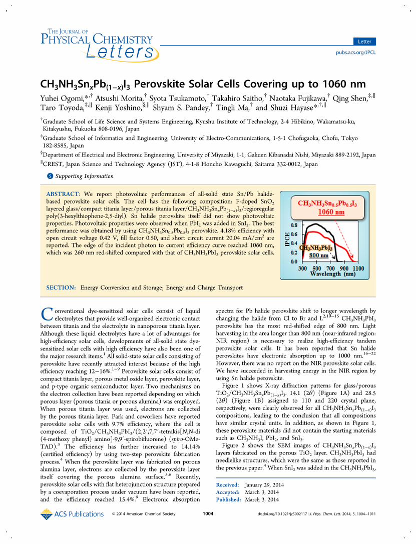
However, there was no report on the NIR perovskite solar cells.We have succeeded in harvesting energy in the NIR region byusing Sn halide perovskite.Figure 1 shows X-ray diffraction patterns for glass/porous
TiO2/CH3NH3SnxPb(1−x)I3. 14.1 (2θ) (Figure 1A) and 28.5(2θ) (Figure 1B) assigned to 110 and 220 crystal plane,respectively, were clearly observed for all CH3NH3SnxPb(1−x)I3compositions, leading to the conclusion that all compositionshave similar crystal units. In addition, as shown in Figure 1,these perovskite materials did not contain the starting materialssuch as CH3NH3I, PbI2, and SnI2.Figure 2 shows the SEM images of CH3NH3SnxPb(1−x)I3
layers fabricated on the porous TiO2 layer. CH3NH3PbI3 hadneedlelike structures, which were the same as those reported inthe previous paper.4 When SnI2 was added in the CH3NH3PbI3,
Received: January 29, 2014Accepted: March 3, 2014Published: March 3, 2014
Letter
pubs.acs.org/JPCL
© 2014 American Chemical Society 1004 dx.doi.org/10.1021/jz5002117 | J. Phys. Chem. Lett. 2014, 5, 1004−1011
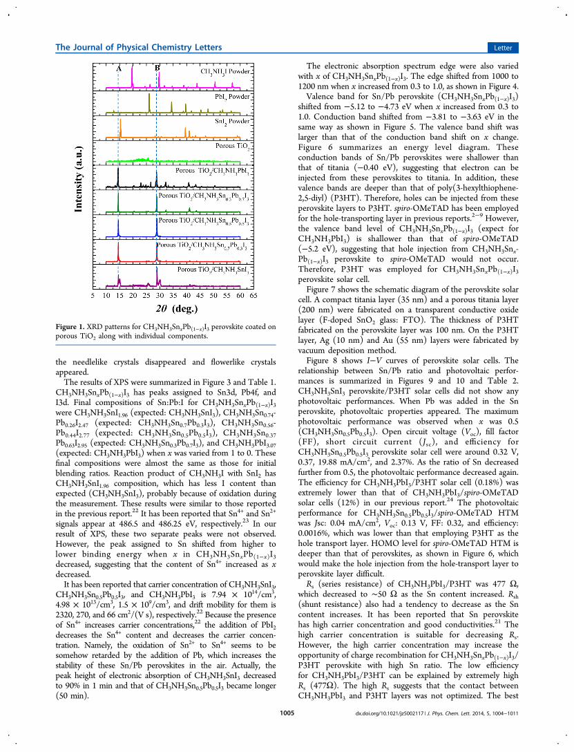
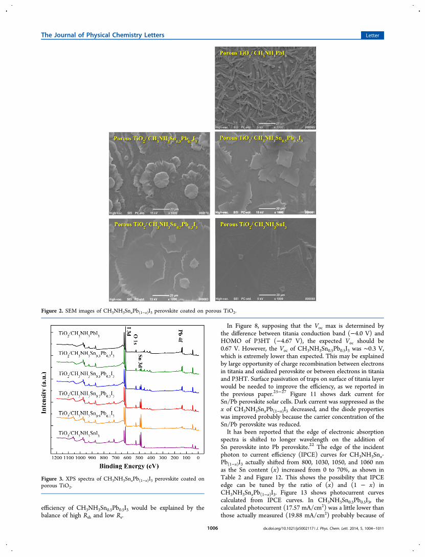
the needlelike crystals disappeared and flowerlike crystalsappeared.The results of XPS were summarized in Figure 3 and Table 1.
CH3NH3SnxPb(1−x)I3 has peaks assigned to Sn3d, Pb4f, andI3d. Final compositions of Sn:Pb:I for CH3NH3SnxPb(1−x)I3were CH3NH3SnI1.96 (expected: CH3NH3SnI3), CH3NH3Sn0.74-Pb0.26I2.47 (expected: CH3NH3Sn0.7Pb0.3I3), CH3NH3Sn0.56-Pb0.44I2.77 (expected: CH3NH3Sn0.5Pb0.5I3), CH3NH3Sn0.37Pb0.63I2.95 (expected: CH3NH3Sn0.3Pb0.7I3), and CH3NH3PbI3.07(expected: CH3NH3PbI3) when x was varied from 1 to 0. Thesefinal compositions were almost the same as those for initialblending ratios. Reaction product of CH3NH3I with SnI2 hasCH3NH3SnI1.96 composition, which has less I content thanexpected (CH3NH3SnI3), probably because of oxidation duringthe measurement. These results were similar to those reportedin the previous report.22 It has been reported that Sn4+ and Sn2+
signals appear at 486.5 and 486.25 eV, respectively.23 In ourresult of XPS, these two separate peaks were not observed.However, the peak assigned to Sn shifted from higher tolower binding energy when x in CH3NH3SnxPb(1−x)I3decreased, suggesting that the content of Sn4+ increased as xdecreased.It has been reported that carrier concentration of CH3NH3SnI3,
CH3NH3Sn0.5Pb0.5I3, and CH3NH3PbI3 is 7.94 × 10¹⁴/cm3,4.98 × 1013/cm3, 1.5 × 10⁹/cm3, and drift mobility for them is2320, 270, and 66 cm2/(V s), respectively.22 Because the presenceof Sn4+ increases carrier concentrations,22 the addition of PbI2decreases the Sn4+ content and decreases the carrier concen-tration. Namely, the oxidation of Sn2+ to Sn4+ seems to besomehow retarded by the addition of Pb, which increases thestability of these Sn/Pb perovskites in the air. Actually, thepeak height of electronic absorption of CH3NH3SnI3 decreasedto 90% in 1 min and that of CH3NH3Sn0.5Pb0.5I3 became longer(50 min).
The electronic absorption spectrum edge were also variedwith x of CH3NH3SnxPb(1−x)I3. The edge shifted from 1000 to1200 nm when x increased from 0.3 to 1.0, as shown in Figure 4.Valence band for Sn/Pb perovskite (CH3NH3SnxPb(1−x)I3)
shifted from −5.12 to −4.73 eV when x increased from 0.3 to1.0. Conduction band shifted from −3.81 to −3.63 eV in thesame way as shown in Figure 5. The valence band shift waslarger than that of the conduction band shift on x change.Figure 6 summarizes an energy level diagram. Theseconduction bands of Sn/Pb perovskites were shallower thanthat of titania (−0.40 eV), suggesting that electron can beinjected from these perovskites to titania. In addition, thesevalence bands are deeper than that of poly(3-hexylthiophene-2,5-diyl) (P3HT). Therefore, holes can be injected from theseperovskite layers to P3HT. spiro-OMeTAD has been employedfor the hole-transporting layer in previous reports.2−9 However,the valence band level of CH3NH3SnxPb(1−x)I3 (expect forCH3NH3PbI3) is shallower than that of spiro-OMeTAD(−5.2 eV), suggesting that hole injection from CH3NH3Snx-Pb(1−x)I3 perovskite to spiro-OMeTAD would not occur.Therefore, P3HT was employed for CH3NH3SnxPb(1−x)I3perovskite solar cell.Figure 7 shows the schematic diagram of the perovskite solar
cell. A compact titania layer (35 nm) and a porous titania layer(200 nm) were fabricated on a transparent conductive oxidelayer (F-doped SnO2 glass: FTO). The thickness of P3HTfabricated on the perovskite layer was 100 nm. On the P3HTlayer, Ag (10 nm) and Au (55 nm) layers were fabricated byvacuum deposition method.Figure 8 shows I−V curves of perovskite solar cells. The
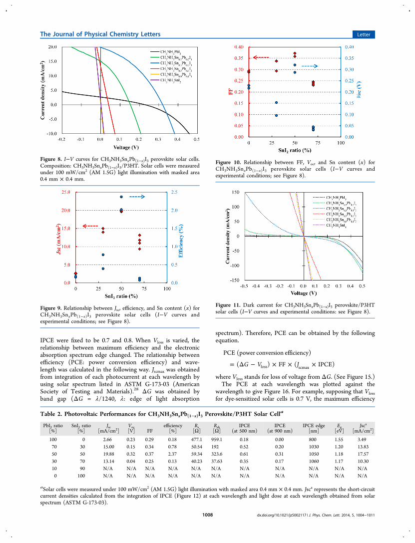
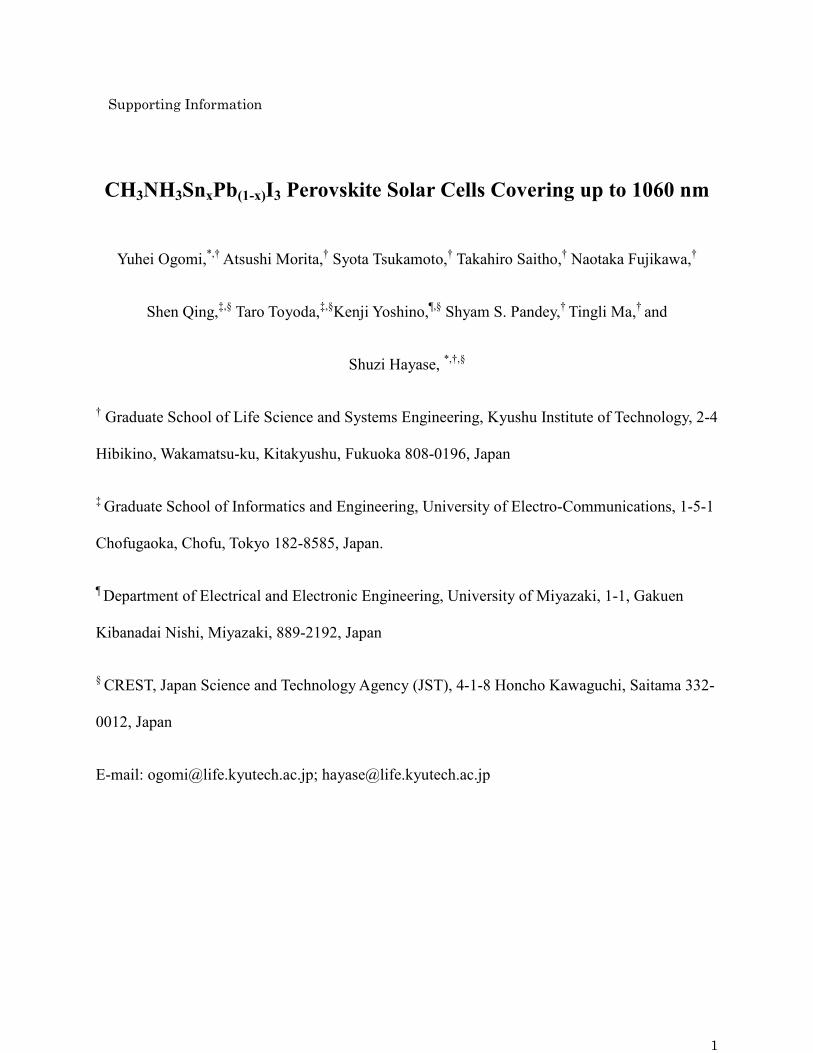
relationship between Sn/Pb ratio and photovoltaic perfor-mances is summarized in Figures 9 and 10 and Table 2.CH3NH3SnI3 perovskite/P3HT solar cells did not show anyphotovoltaic performances. When Pb was added in the Snperovskite, photovoltaic properties appeared. The maximumphotovoltaic performance was observed when x was 0.5(CH3NH3Sn0.5Pb0.5I3). Open circuit voltage (Voc), fill factor(FF), short circuit current (Jsc), and efficiency forCH3NH3Sn0.5Pb0.5I3 perovskite solar cell were around 0.32 V,0.37, 19.88 mA/cm2, and 2.37%. As the ratio of Sn decreasedfurther from 0.5, the photovoltaic performance decreased again.The efficiency for CH3NH3PbI3/P3HT solar cell (0.18%) wasextremely lower than that of CH3NH3PbI3/spiro-OMeTADsolar cells (12%) in our previous report.24 The photovoltaicperformance for CH3NH3Sn0.5Pb0.5I3/spiro-OMeTAD HTMwas Jsc: 0.04 mA/cm2, Voc: 0.13 V, FF: 0.32, and efficiency:0.0016%, which was lower than that employing P3HT as thehole transport layer. HOMO level for spiro-OMeTAD HTM isdeeper than that of perovskites, as shown in Figure 6, whichwould make the hole injection from the hole-transport layer toperovskite layer difficult.Rs (series resistance) of CH3NH3PbI3/P3HT was 477 Ω,
which decreased to ∼50 Ω as the Sn content increased. Rsh(shunt resistance) also had a tendency to decrease as the Sncontent increases. It has been reported that Sn perovskitehas high carrier concentration and good conductivities.21 Thehigh carrier concentration is suitable for decreasing Rs.However, the high carrier concentration may increase theopportunity of charge recombination for CH3NH3SnxPb(1−x)I3/P3HT perovskite with high Sn ratio. The low efficiencyfor CH3NH3PbI3/P3HT can be explained by extremely highRs (477Ω). The high Rs suggests that the contact betweenCH3NH3PbI3 and P3HT layers was not optimized. The best
Figure 1. XRD patterns for CH3NH3SnxPb(1−x)I3 perovskite coated onporous TiO2 along with individual components.
The Journal of Physical Chemistry Letters Letter
dx.doi.org/10.1021/jz5002117 | J. Phys. Chem. Lett. 2014, 5, 1004−10111005
efficiency of CH3NH3Sn0.5Pb0.5I3 would be explained by thebalance of high Rsh and low Rs.
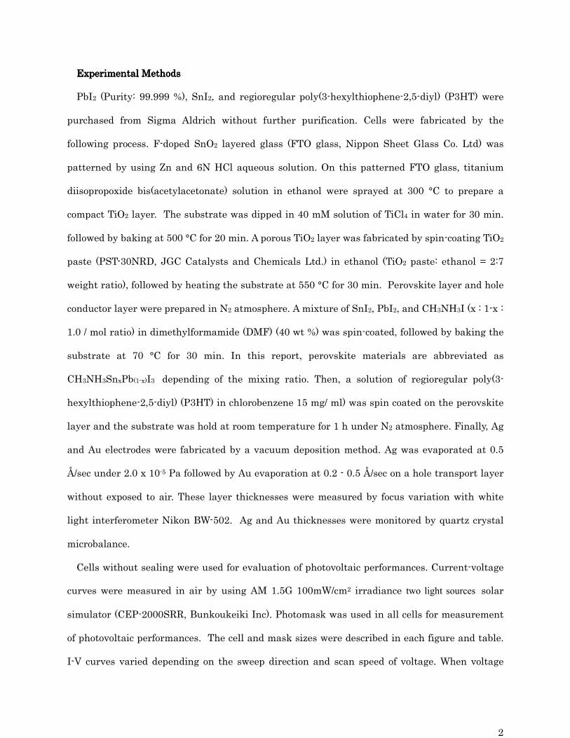
In Figure 8, supposing that the Voc max is determined bythe difference between titania conduction band (−4.0 V) andHOMO of P3HT (−4.67 V), the expected Voc should be0.67 V. However, the Voc of CH3NH3Sn0.5Pb0.5I3 was ∼0.3 V,which is extremely lower than expected. This may be explainedby large opportunity of charge recombination between electronsin titania and oxidized perovskite or between electrons in titaniaand P3HT. Surface passivation of traps on surface of titania layerwould be needed to improve the efficiency, as we reported inthe previous paper.25−27 Figure 11 shows dark current forSn/Pb perovskite solar cells. Dark current was suppressed as thex of CH3NH3SnxPb(1−x)I3 decreased, and the diode propertieswas improved probably because the carrier concentration of theSn/Pb perovskite was reduced.It has been reported that the edge of electronic absorption
spectra is shifted to longer wavelength on the addition ofSn perovskite into Pb perovskite.22 The edge of the incidentphoton to current efficiency (IPCE) curves for CH3NH3Snx-Pb(1−x)I3 actually shifted from 800, 1030, 1050, and 1060 nmas the Sn content (x) increased from 0 to 70%, as shown inTable 2 and Figure 12. This shows the possibility that IPCEedge can be tuned by the ratio of (x) and (1 − x) inCH3NH3SnxPb(1−x)I3. Figure 13 shows photocurrent curvescalculated from IPCE curves. In CH3NH3Sn0.5Pb0.5I3, thecalculated photocurrent (17.57 mA/cm2) was a little lower thanthose actually measured (19.88 mA/cm2) probably because of
Figure 3. XPS spectra of CH3NH3SnxPb(1−x)I3 perovskite coated onporous TiO2.
Figure 2. SEM images of CH3NH3SnxPb(1−x)I3 perovskite coated on porous TiO2.
The Journal of Physical Chemistry Letters Letter
dx.doi.org/10.1021/jz5002117 | J. Phys. Chem. Lett. 2014, 5, 1004−10111006
easier oxidation of these perovskites with large x ratio duringIPCE measurements.Figure 14 and Table 3 show the optimized characteristics for
CH3NH3Sn0.5Pb0.5I3/P3HT and CH3NH3PbI3/spiro-OMeTADwith 12% efficiency in our previous report.24 Voc, FF, Jsc, andefficiency for CH3NH3Sn0.5Pb0.5I3/P3HT were 0.42 V, 0.50,20.04 mA/cm2, and 4.18%. CH3NH3Sn0.5Pb0.5I3/P3HT canharvest light in the area from 800 to 1060 nm, where previousPb-based solar cells were not able to. Rsh of CH3NH3Sn0.5Pb0.5I3/P3HT was 1402 Ω, which was seriously lower than that of71320 Ω for CH3NH3PbI3-based solar cell. As discussed in theprevious session, retardation of charge recombination is neededto increase the efficiency further.Figure 15 shows the energy level diagrams for dye-sensitized
solar cells with iodide/triiodide redox species, conventional
organic thin film solar cells and perovskite solar cells. In eachsolar cell, observed Voc is lower than that expected from thelight absorption edge. The difference between the observed Vocand that expected from the light-absorption spectrum edge(ΔG = 1240/light absorption edge (nm)) is called Vloss. TheVloss for dye-sensitized solar cells with iodide/triiodide andorganic thin film solar cells is ∼0.7 V.29 For example, in the caseof dye-sensitized solar cell consisting of iodide/triiodide redoxspecies, Vloss (0.7 V) was estimated by summarizing ΔG1 (energyloss caused by electron injection from dye to titania), ΔG2(energy loss caused by electron injection from iodide to oxidizeddye), and ΔGx (energy loss caused by charge recombination).Vloss for perovskite solar cells is expected to be 0.5 V, which islower than that with iodide/triiodide redox species.29
Figure 16 shows the relationship between efficiency andelectronic absorption spectrum edge when FF and average
Table 1. XPS Analysis of CH3NH3SnxPb(1−x)I3 Perovskite Coated on Porous TiO2a
binding energy/eV CH3NH3SnxPbyIz
Sn 3d3/2 Sn 3d5/2 Pb 4f5/2 Pb 4f7/2 I 3d3/2 I 3d5/2 x y z
CH3NH3PbI3 N/A N/A 140.08 135.11 627.40 615.94 0.00 1.00 3.07CH3NH3Sn0.3Pb0.7I3 492.33 483.90 139.69 134.71 627.06 615.61 0.37 0.63 2.95CH3NH3Sn0.5Pb0.5I3 492.60 484.18 139.76 134.77 627.22 615.77 0.56 0.44 2.77CH3NH3Sn0.7Pb0.3I3 492.61 484.20 139.88 134.84 627.52 616.04 0.74 0.26 2.47CH3NH3Sn0.9Pb0.1I3 492.68 484.27 139.95 135.01 627.78 616.36 0.91 0.09 2.29CH3NH3SnI3 492.91 484.52 N/A N/A 628.43 616.94 1.00 0.00 1.96
aRatio of x, y, and z were obtained from integration of the peak area of corresponding XPS peaks.
Figure 4. Electronic absorption spectra of CH3NH3SnxPb(1−x)I3perovskite coated on porous TiO2.
Figure 5. Energy diagram for CH3NH3SnxPb(1−x)I3 perovskite.
Figure 6. Energy diagram of titania, P3HT, spiro-OMeTAD, andCH3NH3SnxPb(1−x)I3 perovskite.
Figure 7. Structure of CH3NH3SnxPb(1−x)I3 perovskite solar cells.
The Journal of Physical Chemistry Letters Letter
dx.doi.org/10.1021/jz5002117 | J. Phys. Chem. Lett. 2014, 5, 1004−10111007
IPCE were fixed to be 0.7 and 0.8. When Vloss is varied, therelationship between maximum efficiency and the electronicabsorption spectrum edge changed. The relationship betweenefficiency (PCE: power conversion efficiency) and wave-length was calculated in the following way. Jscmax was obtainedfrom integration of each photocurrent at each wavelength byusing solar spectrum listed in ASTM G-173-03 (AmericanSociety of Testing and Materials).28 ΔG was obtained byband gap (ΔG = λ/1240, λ: edge of light absorption
spectrum). Therefore, PCE can be obtained by the followingequation.
= Δ − × × ×G V J
PCE (power conversion efficiency)
( ) FF ( IPCE)loss scmax
where Vloss stands for loss of voltage from ΔG. (See Figure 15.)The PCE at each wavelength was plotted against the
wavelength to give Figure 16. For example, supposing that Vlossfor dye-sensitized solar cells is 0.7 V, the maximum efficiency
Figure 8. I−V curves for CH3NH3SnxPb(1−x)I3 perovskite solar cells.Composition: CH3NH3SnxPb(1−x)I3/P3HT. Solar cells were measuredunder 100 mW/cm2 (AM 1.5G) light illumination with masked area0.4 mm × 0.4 mm.
Table 2. Photovoltaic Performances for CH3NH3SnxPb(1−x)I3 Perovskite/P3HT Solar Cella
PbI2 ratio[%]
SnI2 ratio[%]
Jsc[mA/cm2]
Voc[V] FF
efficiency[%]
Rs[Ω]
Rsh[Ω]
IPCE(at 500 nm)
IPCE(at 900 nm)
IPCE edge[nm]
Eg[eV]
Jsca
[mA/cm2]
100 0 2.66 0.23 0.29 0.18 477.1 959.1 0.18 0.00 800 1.55 3.4970 30 15.00 0.15 0.34 0.78 50.54 192 0.52 0.20 1030 1.20 13.8350 50 19.88 0.32 0.37 2.37 59.34 323.6 0.61 0.31 1050 1.18 17.5730 70 13.14 0.04 0.25 0.13 40.23 37.63 0.35 0.17 1060 1.17 10.3010 90 N/A N/A N/A N/A N/A N/A N/A N/A N/A N/A N/A0 100 N/A N/A N/A N/A N/A N/A N/A N/A N/A N/A N/A
aSolar cells were measured under 100 mW/cm2 (AM 1.5G) light illumination with masked area 0.4 mm × 0.4 mm. Jsca represents the short-circuitcurrent densities calculated from the integration of IPCE (Figure 12) at each wavelength and light dose at each wavelength obtained from solarspectrum (ASTM G-173-03).
Figure 9. Relationship between Jsc, efficiency, and Sn content (x) forCH3NH3SnxPb(1−x)I3 perovskite solar cells (I−V curves andexperimental conditions; see Figure 8).
Figure 10. Relationship between FF, Voc, and Sn content (x) forCH3NH3SnxPb(1−x)I3 perovskite solar cells (I−V curves andexperimental conditions; see Figure 8).
Figure 11. Dark current for CH3NH3SnxPb(1−x)I3 perovskite/P3HTsolar cells (I−V curves and experimental conditions: see Figure 8).
The Journal of Physical Chemistry Letters Letter
dx.doi.org/10.1021/jz5002117 | J. Phys. Chem. Lett. 2014, 5, 1004−10111008

(13%) is obtained by using dyes, which can harvest the light upto 800 nm (0.7 (Vloss) in Figure 15). In the case of perovskite-sensitized solar cells, supposing that Voc loss is 0.5 V, maximumefficiency (16.6%) can be obtained by 900 nm light absorptionedge (0.5 (Vloss) in Figure 15). The value of 0.5 V loss wastaken from the previous paper.29 When the light absorptionedge is further shifted to longer wavelength, the efficiencydecreased again, as shown in Figure 16. The edge of the IPCEcurve for CH3NH3PbI3-sensitized solar cells is limited to800 nm. If the light absorption edge is optimized to be 900 nmby adjusting Pb/Sn ratio, further enhancement of solar cellefficiency is expected. Of course, these Sn/Pb solar cells havingsensitivity in the area of IR regions are useful for bottom cellsfor all-solid-type perovskite tandem cells.
Figure 12. IPCE curves for CH3NH3SnxPb(1−x)I3 perovskite/P3HTsolar cells (I−V curves and experimental conditions: see Figure 8).
Figure 13. IPCE spectrum for CH3NH3Sn0.5Pb0.5I3 perovskite solarcell. Calculated Jsca represents the short-circuit current densitiescalculated from the integration of IPCE (Figure 12) at eachwavelength and light loss at each wavelength obtained from solarspectrum (ASTM G-173-03). See the experimental section in theSupporting Information.
Figure 14. Optimized photovoltaic performance (A) I−V and (B) IPCE curves for CH3NH3Sn0.5Pb0.5I3/P3HT and CH3NH3PbI3/spiro-OMeTADperovskite solar cells. (See Figure 8 for experimental conditions.)
Table 3. Photovoltaic Performances for Perovskite Solar Cells Using CH3NH3Sn0.5Pb0.5I3/P3HT and CH3NH3PbI3/spiro-OMeTADa
Jsc [mA/cm2] Voc [V] FF efficiency [%] Rs [Ω] Rsh [Ω] Jsc
a [mA/cm2]
CH3NH3PbI3/spiro-OMeTAD 19.20 1.00 0.62 11.98 112.9 71320 18.01CH3NH3Sn0.5Pb0.5I3/P3HT 20.04 0.42 0.50 4.18 50 1402 18.43
aSolar cells were measured under 100 mW/cm2 (AM 1.5G) light illumination with masked area 0.4 mm × 0.4 mm. Jsca represents the short circuit
current densities calculated from the integration of IPCE (Figure 14B) at each wavelength and light dose at each wavelength obtained from solarspectrum (ASTM G-173-03). These data were obtained from Figure 14.
Figure 15. Energy diagrams for (A) dye-sensitized solar cells withiodine/iodide, (B) organic thin film solar cell (OPV), and (C)perovskite solar cell that are focused on voltage losses.
The Journal of Physical Chemistry Letters Letter
dx.doi.org/10.1021/jz5002117 | J. Phys. Chem. Lett. 2014, 5, 1004−10111009

Photovoltaic performances for all solid-state Sn/Pb basedperovskite solar cells were reported for the first time. It wasproved that the cell can harvest the light in the area up to1060 nm. The Sn/Pb-based perovskite solar cells are useful forbottom cells for tandem perovskite solar cells. To increase theefficiency, we concluded that retardation of charge recombina-tion and increase in the Rsh are needed.
■ ASSOCIATED CONTENT*S Supporting InformationExperimental methods. This material is available free of chargevia the Internet at http://pubs.acs.org.
■ AUTHOR INFORMATIONCorresponding Authors*E-mail: [email protected] (Y.O.).*E-mail: [email protected] (S.H.).NotesThe authors declare no competing financial interest.
■ ACKNOWLEDGMENTSThis research was supported by JST and CREST.
■ REFERENCES(1) Hagfeldt, A.; Boschloo, G.; Sun, L.; Kloo, L.; Pettersson, H. Dye-Sensitized Solar Cells. Chem. Rev. 2010, 110, 6595−6630.(2) Noh, J. H.; m, S. H.; Heo, J. H.; Mandal, T. N.; Seok, S. I.Chemical Management for Colorful, Efficient, And Stable Inorganic−organic Hybrid Nanostructured Solar Cells. Nano Lett. 2013, 13,1764−1769.(3) Kim, H.-S.; Lee, C.-R.; Im, J.-H.; Lee, K.-B.; Moehl, T.;Marchioro, A.; Moon, S.-J.; Humphry-Baker, R.; Yum, J.-H.; Moser,J. E.; Graetzel, M.; Park, N.-G. Lead Iodide Perovskite SensitizedAll-Solid-State Submicron Thin Film Mesoscopic Solar Cell withEfficiency Exceeding 9%. Sci. Rep. 2012, 2, 591.(4) Burschka, J.; Pellet, N.; Moon, S. J.; Baker, R. H.; Gao, P.;Nazeeruddin, M. K.; Graetzel, M. Sequential Deposition As a Route toHigh-Performance Perovskite-Sensitized Solar Cells. Nature 2013,499, 316−319.
(5) Lee, M. M.; Teuscher, J.; Miyasaka, T.; Murakami, T. N.; Snaith,H. J. Efficient Hybrid Solar Cells Based on Meso-SuperstructuredOrganometal Halide Perovskites. Science 2012, 338, 643−647.(6) Ball, J. M.; Lee, M. M.; Hey, A.; Snaith, H. J. Low-TemperatureProcessed Mesosuperstructured to Thin-Film Perovskite Solar Cells.Energy Environ. Sci. 2013, 6, 1739−1743.(7) Liu, D.; Kelly, T. L. Perovskite Solar Cells with a PlanarHeterojunction Structure Prepared Using Room-Temperature Sol-ution Processing Techniques. Nat. Photonics 2014, 8, 133−138.(8) Snaith, H. J. Perovskites: The Emergence of a New Era for Low-Cost, High-Efficiency Solar Cells. J. Phys. Chem. Lett. 2013, 4, 3623−3630.(9) Liu, M.; Johnston, M. B.; Snaith, H. J. Efficient PlanarHeterojunction Perovskite Solar Cells by Vapour Deposition. Nature2013, 501, 395−398.(10) Kojima, A.; Teshima, K.; Shirai, Y.; Miyasaka, T. OrganometalHalide Perovskites as Visible-Light Sensitizers for Photovoltaic Cells. J.Am. Chem. Soc. 2009, 131, 6050−6051.(11) Im, J.-H.; Lee, C.-R.; Lee, J.-W.; Park, S.-W.; Park, N.-G. 6.5%Efficient Perovskite Quantum-Dot-Sensitized Solar Cell. Nanoscale2011, 3, 4088−4093.(12) Tanaka, K.; Takahashi, T.; Ban, T.; Kondo, T.; Uchida, K.;Miura, N. Comparative Study on the Excitons in Lead-Halide-BasedPerovskite-Type Crystals CH3NH3PbBr3 CH3NH3PbI3. Solid StateCommun. 2003, 127, 619−623.(13) Calabrese, J.; Jones, N. L.; Harlow, R. L.; Herron, N.; Thorn, D.L.; Wang, Y. Preparation and Characterization of Layered Lead HalideCompounds. J. Am. Chem. Soc. 1991, 113, 2328−2330.(14) Mosconi, E.; Amat, A.; Nazeeruddin, M. K.; Gratzel, M.;Angelis, F. D. First-Principles Modeling of Mixed Halide OrganometalPerovskites for Photovoltaic Applications. J. Phys. Chem. C 2013, 117,13902−13913.(15) Onoda-Yamaura, N.; Matsuo, T.; Suga, H. Dielectric Study ofCH3NH3PbX3 (X = Cl, Br, I). J. Phys. Chem. Solids 1992, 53, 935−939.(16) Mitzi, D. B.; Feild, C. A.; Harrison, W. T. A.; Guloy, A. M.Conducting Tin Halides with a Layered Organic-Based PerovskiteStructure. Nature 1994, 369, 467−469.(17) Mitzi, D. B.; Wang, S.; Feild, C. A.; Chess, C. A.; Guloy, A. M.Conducting Layered Organic-Inorganic Halides Containing <110>-Oriented Perovskite Sheets. Science 1995, 267, 1473−1476.(18) Mitzi, D. B.; Feild; Schlesinger, Z.; Laibowitz, R. B. Transport,Optical, and Magnetic Properties of the Conducting Halide PerovskiteCH3NH3SnI3. J. Solid State Chem. 1995, 114, 159−163.(19) Clark, S. J.; Donaldson, J. D.; Harvey, J. A. Evidence for theDirect Population of Solid-State Bands by Non-Bonding Electron Pairsin Compounds of the Type CsMIIX3(MII= Ge, Sn, Pb; X = Cl, Br, I).J. Mater. Chem. 1995, 5, 1813−1818.(20) Song, I.; J., H.; Im, J.; Androulakis, J.; Malliakas, C. D.; Li, H.;Freeman, A. J.; Kenney, J. T.; Kanatzidis, M. G. CsSnI3: Semi-conductor or Metal? High Electrical Conductivity and Strong Near-Infrared Photoluminescence from a Single Material. High HoleMobility and Phase-Transitions. J. Am. Chem. Soc. 2012, 134, 8579−8587.(21) Takahashi, Y.; Hasegawa, H.; Takahashi, Y.; Inabe, T. HallMobility in Tin Iodide Perovskite CH3NH3SnI3: Evidence for aDoped Semiconductor. J. Solid State Chem. 2013, 205, 39−43.(22) Stoumpos, C. C.; Malliakas, C. D.; Kanatzidis, M. G.Semiconducting Tin and Lead Iodide Perovskites with OrganicCations: Phase Transitions, High Mobilities, And near-InfraredPhotoluminescent Properties. Inorg. Chem. 2013, 52, 9019−9038.(23) Moulder, J. F. Handbook of X-ray Photoelectron Spectroscopy;Perkin-Elmer Corp.: Eden, Prairie, 1992.(24) Kukihara, K.; Ogomi, Y.; Shen. Q.; Toyota, T.; Yoshino, K.;Pandey, S. S.; Hayase, S. All-Solid Dye-Sensitized Solar CellsConsisting of Passivated Metal Oxide Semiconductor. MRS FallMeeting and Exhibit, Boston, MA, Dec 16, 2013; No. Y5.01.(25) Kukihara, K.; Ogomi, Y.; Shen, Q.; Saito, T.; Yoshino, K.;Pandey, S. S.; Toyoda, T.; Momose, H.; Hayase, S. All Solid
Figure 16. Relationship between light harvesting edge (nm) and solarcell efficiency when voltage loss was varied from 1.0 to 0 V.
The Journal of Physical Chemistry Letters Letter
dx.doi.org/10.1021/jz5002117 | J. Phys. Chem. Lett. 2014, 5, 1004−10111010

Dye-Sensitized Solar Cells with Perovskite Material. PVSEC-23Proceedings, Taipei, Taiwan, Oct 28−Nov 1, 2013, 5-O-11.(26) Ogomi, Y.; Kukihara, K.; Shen, Q.; Toyoda, T.; Yoshino, K.;Pandey, S. S.; Momose, H.; Hayase, S. Control of Charge Dynamics byCharge Separation Interface for All-Solid Perovskite Sensitized SolarCells. ChemPhysChem. 2014, in press.(27) Ogomi, Y.; Sakaguchi, S.; Kado, T.; Kono, M.; Yamaguchi, Y.;Hayase, S. Ru Dye Uptake under Pressurized CO2 Improvement ofPhotovoltaic Performances for Dye-Sensitized Solar Cells. J. Electro-chem. Soc. 2006, 153, A2294−A2297.(28) ASTM G173-03 Reference Spectra Derived from SMARTS v.2.9.2. http://rredc.nrel.gov/solar/spectra/am1.5/ASTMG173/ASTMG173.html.(29) Nayak, P. K.; Cahen, D. Updated Assessment of Possibilities andLimits for Solar Cells. Adv. Mater. 2014, DOI: 10.1002/adma.201304620.
The Journal of Physical Chemistry Letters Letter
dx.doi.org/10.1021/jz5002117 | J. Phys. Chem. Lett. 2014, 5, 1004−10111011
1
Supporting Information
CH3NH3SnxPb(1-x)I3 Perovskite Solar Cells Covering up to 1060 nm
Yuhei Ogomi,*,† Atsushi Morita,
† Syota Tsukamoto,
† Takahiro Saitho,
† Naotaka Fujikawa,
†
Shen Qing,‡,§ Taro Toyoda,
‡,§Kenji Yoshino,
¶,§ Shyam S. Pandey,
† Tingli Ma,
† and
Shuzi Hayase, *,†,§
† Graduate School of Life Science and Systems Engineering, Kyushu Institute of Technology, 2-4
Hibikino, Wakamatsu-ku, Kitakyushu, Fukuoka 808-0196, Japan
‡ Graduate School of Informatics and Engineering, University of Electro-Communications, 1-5-1
Chofugaoka, Chofu, Tokyo 182-8585, Japan.
¶ Department of Electrical and Electronic Engineering, University of Miyazaki, 1-1, Gakuen
Kibanadai Nishi, Miyazaki, 889-2192, Japan
§ CREST, Japan Science and Technology Agency (JST), 4-1-8 Honcho Kawaguchi, Saitama 332-
0012, Japan
E-mail: [email protected]; [email protected]
2
Experimental Experimental Experimental Experimental MethodsMethodsMethodsMethods
PbI2 (Purity: 99.999 %), SnI2, and regioregular poly(3-hexylthiophene-2,5-diyl) (P3HT) were
purchased from Sigma Aldrich without further purification. Cells were fabricated by the
following process. F-doped SnO2 layered glass (FTO glass, Nippon Sheet Glass Co. Ltd) was
patterned by using Zn and 6N HCl aqueous solution. On this patterned FTO glass, titanium
diisopropoxide bis(acetylacetonate) solution in ethanol were sprayed at 300 °C to prepare a
compact TiO2 layer. The substrate was dipped in 40 mM solution of TiCl4 in water for 30 min.
followed by baking at 500 °C for 20 min. A porous TiO2 layer was fabricated by spin-coating TiO2
paste (PST-30NRD, JGC Catalysts and Chemicals Ltd.) in ethanol (TiO2 paste: ethanol = 2:7
weight ratio), followed by heating the substrate at 550 °C for 30 min. Perovskite layer and hole
conductor layer were prepared in N2 atmosphere. A mixture of SnI2, PbI2, and CH3NH3I (x : 1-x :
1.0 / mol ratio) in dimethylformamide (DMF) (40 wt %) was spin-coated, followed by baking the
substrate at 70 °C for 30 min. In this report, perovskite materials are abbreviated as
CH3NH3SnxPb(1-x)I3 depending of the mixing ratio. Then, a solution of regioregular poly(3-
hexylthiophene-2,5-diyl) (P3HT) in chlorobenzene 15 mg/ ml) was spin coated on the perovskite
layer and the substrate was hold at room temperature for 1 h under N2 atmosphere. Finally, Ag
and Au electrodes were fabricated by a vacuum deposition method. Ag was evaporated at 0.5
Å/sec under 2.0 x 10⁻⁵ Pa followed by Au evaporation at 0.2 - 0.5 Å/sec on a hole transport layer
without exposed to air. These layer thicknesses were measured by focus variation with white
light interferometer Nikon BW-502. Ag and Au thicknesses were monitored by quartz crystal
microbalance.
Cells without sealing were used for evaluation of photovoltaic performances. Current-voltage
curves were measured in air by using AM 1.5G 100mW/cm2 irradiance two light sources solar
simulator (CEP-2000SRR, Bunkoukeiki Inc). Photomask was used in all cells for measurement
of photovoltaic performances. The cell and mask sizes were described in each figure and table.
I-V curves varied depending on the sweep direction and scan speed of voltage. When voltage

3
was swept from + to -, charge-up occurred and fill factor increased, leading to higher efficiency.
Therefore, we swept the voltage from – to + direction with 100 msec delay so as to retard
efficiency increase caused by the charge-up phenomena. Incident photon to current efficiency
(IPCE) was measured by using CEP-2000SRR (Bunko Keiki) equipped with 300 W Xe lamp.
Monochromatic light was exposed by DC mode and the current was taken every 100msec after
the light exposure (10 nm interval). The monochromatic light was adjusted to 1 x 10¹⁶ mW/cm2
which was monitored by Si photodiode. IPCE was calculated by the following equation.
IPCE = Ne/Np
where Ne and Np stand for exposure light dose and photocurrent respectively.
The series resistance (Rs) and shunt resistant (Rsh) were measured from current-voltage
curves for solar cells. Rs (V/I) was obtained by the slope near I=0 and Rsh (V/I) was taken from
the slope near V=0. Least-squares method was used for the calculation.
The X-ray diffraction patterns for glass/TiO2/CH3NH3SnxPb(1-x)I3 samples were measured by
RINT-Ultima III, Rigaku.
The valence band level for the Sn/Pb perovskite on porous TiO2 and P3HT film on a glass
substrate (not device structure) were measured by using Photo-Electron Spectroscopy in Air
(PESA)( AC3, RIKEN-KEIKI) . Conduction band level was calculated by taking the
absorption spectrum edge as the band gap and the band gap energy was added to the valence
band level measured by AC3. Energy levels for spiro-OMeTAD was taken from the previous
paper .1
References
(1) Kim, H.-S.; Lee, C.-R.; Im, J.-H.; Lee, K.-B.; Moehl, T.; Marchioro, A.; Moon, S.-J.; Humphry-Baker,
R.; Yum, J.-H.; Moser, J. E. Lead Iodide Perovskite Sensitized All-Solid-State Submicron Thin Film
Mesoscopic Solar Cell with Efficiency Exceeding 9%. Sci. Rep. 2012, 2, 591.