disclaimer - scholarworks.unist.ac.krscholarworks.unist.ac.kr/bitstream/201301/5483/1/a...
TRANSCRIPT

저 시-비 리- 경 지 2.0 한민
는 아래 조건 르는 경 에 한하여 게
l 저 물 복제, 포, 전송, 전시, 공연 송할 수 습니다.
다 과 같 조건 라야 합니다:
l 하는, 저 물 나 포 경 , 저 물에 적 된 허락조건 명확하게 나타내어야 합니다.
l 저 터 허가를 면 러한 조건들 적 되지 않습니다.
저 에 른 리는 내 에 하여 향 지 않습니다.
것 허락규약(Legal Code) 해하 쉽게 약한 것 니다.
Disclaimer
저 시. 하는 원저 를 시하여야 합니다.
비 리. 하는 저 물 리 목적 할 수 없습니다.
경 지. 하는 저 물 개 , 형 또는 가공할 수 없습니다.

A Comprehensive Study of Dual Active Bridge Converter and Deep Belief Network Controller for
Bi-directional Solid State Transformer
Kim, Sul-Gi
School of Electrical and Computer Engineering (Electrical Engineering)
Ulsan National Institute of Science and Technology 2014

A Comprehensive Study of Dual Active Bridge Converter and Deep Belief Network Controller for
Bi-directional Solid State Transformer
Kim, Sul-Gi
School of Electrical and Computer Engineering (Electrical Engineering)
Graduate School of UNIST
2014
I
A Comprehensive Study of Dual Active Bridge Converter and Deep Belief Network Controller for
Bi-directional Solid State Transformer
Kim, Sul-Gi
School of Electrical and Computer Engineering (Electrical Engineering)
Graduate School of UNIST
II

A Comprehensive Study of Dual Active Bridge Converter and Deep Belief Network Controller for
Bi-directional Solid State Transformer
A thesis submitted to the Graduate School of UNIST
in partial fulfillment of the requirements for the degree of
Master of Engineering
Kim, Sul-Gi
06. 19. 2014 Approved by
___________________________
Major Advisor Jung, Jeehoon
III

A Comprehensive Study of Dual Active Bridge Converter and Deep Belief Network Controller for
Bi-directional Solid State Transformer
Kim, Sul-Gi
This certifies that the thesis of Kim, Sul Gi is approved.
06. 19. 2014
___________________________
Advisor: Jung, Jeehoon
___________________________
Han, Ki Jin
___________________________
Choi, Jaesik
IV

Abstract
This dissertation presents a comprehensive study of Dual Active Bridge (DAB) converter and
Deep Belief Network (DBN) controller for bi-directional Solid State Transformers (SSTs).
The first contribution is to propose a dc-dc DAB converter as a single stage SST. The proposed
converter topology consists of two active H-bridges and one high-frequency transformer. Output
voltage can be regulated when input voltage changes by phase shift modulation. Power is transferred
from the first bridge to the second bridge. It analyzes the steady-state operation.
The second contribution is to develop an average model for dc-dc DAB converters. The
transformer current in DAB converter is purely ac, making continuous-time modeling is difficult.
Instead, the proposed approach uses the only 1st order terms of transformer current and capacitor
voltage as state variables.
The third contribution is the controller design of a dc-dc DAB converter. The PI gains are allowed
to vary within a predetermined range and therefore eliminate the problems from the conventional PI
controller. The performance of the proposed artificial intelligence gain scheduled PI controller is
simulated and compared with the conventional fixed PI controller under steady state error,
responding time and load disturbances.
The experimental system of DAB converter is implemented using digital signal processing unit,
Texas Instrument TMS320F28335 control board, to examine and verify the performance of the
proposed controller under various operating conditions. Simulation and experimental results show a
good improvement in transient as well as steady state response of the proposed controller. However,
power efficiency, computation burden and complexity of algorithm are disadvantage of proposed
algorithm.
V
Contents
I. Introduction ..................................................................................................................................... 1
1.1 Solid State Transformers .......................................................................................................... 2
1.2 Candidate Circuit Configurations ............................................................................................. 3
1.3 Analysis and Applications of DAB Converters ....................................................................... 4
1.4 Modeling of Power Converters ................................................................................................ 5
1.5 Control of Power Converters .................................................................................................... 7
II. Dual Active Bridge Converters ................................................................................................... 10
2.1 Circuit Configuration ............................................................................................................. 10
2.2 Dual Active Bridge Converter Model .................................................................................... 12
III. Deep Belief Network Controller ................................................................................................ 20
3.1 Perceptrons ............................................................................................................................. 20
3.2 Feed-forward Networks .......................................................................................................... 21
3.3 Training .................................................................................................................................. 23
3.4 Restricted Boltzmann Machines ............................................................................................. 24
3.4 Contrastive Divergence .......................................................................................................... 25
3.5 Deep Belief Networks ............................................................................................................ 26
3.6 Deep Belief Network Controller in Dual Active Bridge Converter ....................................... 27
IV. Simulation and Experiment ........................................................................................................ 29
4.1 Circuit Configuration ............................................................................................................. 29
4.2 Controller Configuration ........................................................................................................ 31
4.3 Simulation and Experimental Results .................................................................................... 35
V. Discussion and Conclusion ......................................................................................................... 39
5.1 Future Work ........................................................................................................................... 39
References ........................................................................................................................................ 41
Appendix .......................................................................................................................................... 51
Acknowledgement ............................................................................................................................ 80
VI

List of Figures
Figure 1. Centralized (Left) and Decentralized (Right) Energy Network System [123] .................... 1
Figure 2. The Applications of Smart Solid-State Transformers [124] ................................................ 2
Figure 3. DAB Converter Topology ................................................................................................... 3
Figure 4. CLLC Converter Topology.................................................................................................. 3
Figure 5. Actual Waveform and Averaged Waveform ....................................................................... 6
Figure 6. Comparison between Open and Closed Loop Control ........................................................ 7
Figure 7. The Circuit Schematic of DAB Converter ......................................................................... 10
Figure 8. Positive Power Flow (Left) and Negative Power Flow (Right) of DAB Converter .......... 11
Figure 9. Heavy Load Waveform...................................................................................................... 12
Figure 10. Medium Load Waveform ................................................................................................ 12
Figure 11. Light Load Waveform ..................................................................................................... 13
Figure 12. Equivalent Circuit during t0 ~ t1 [126] ........................................................................... 13
Figure 13. Equivalent Circuit during t1 ~ t2 [126] ........................................................................... 14
Figure 14. Equivalent Circuit during t2 ~ t3 [126] ........................................................................... 14
Figure 15. The Equivalent Circuit during t3 ~ t4 [126] .................................................................... 15
Figure 16. The Equivalent Circuit during t4 ~ t5 [126] .................................................................... 15
Figure 17. Equivalent Circuit during t5 ~t6 [126] ............................................................................ 15
Figure 18. Small-Signal Schematic of Closed-loop Controlled DAB .............................................. 19
Figure 19. Linear Classifier Example ............................................................................................... 20
Figure 20. XOR Problem Example ................................................................................................... 21
Figure 21. Feed-forward Network .................................................................................................... 22
Figure 22. Global and Local Optimization Problem ......................................................................... 23
Figure 23. Interaction between Visible Layer and Hidden Layer in DBN [109] .............................. 24
Figure 24. Contrastive Divergence Example [125] ........................................................................... 25
Figure 25. Example of Training RBM for Predicting y [108] ........................................................... 26
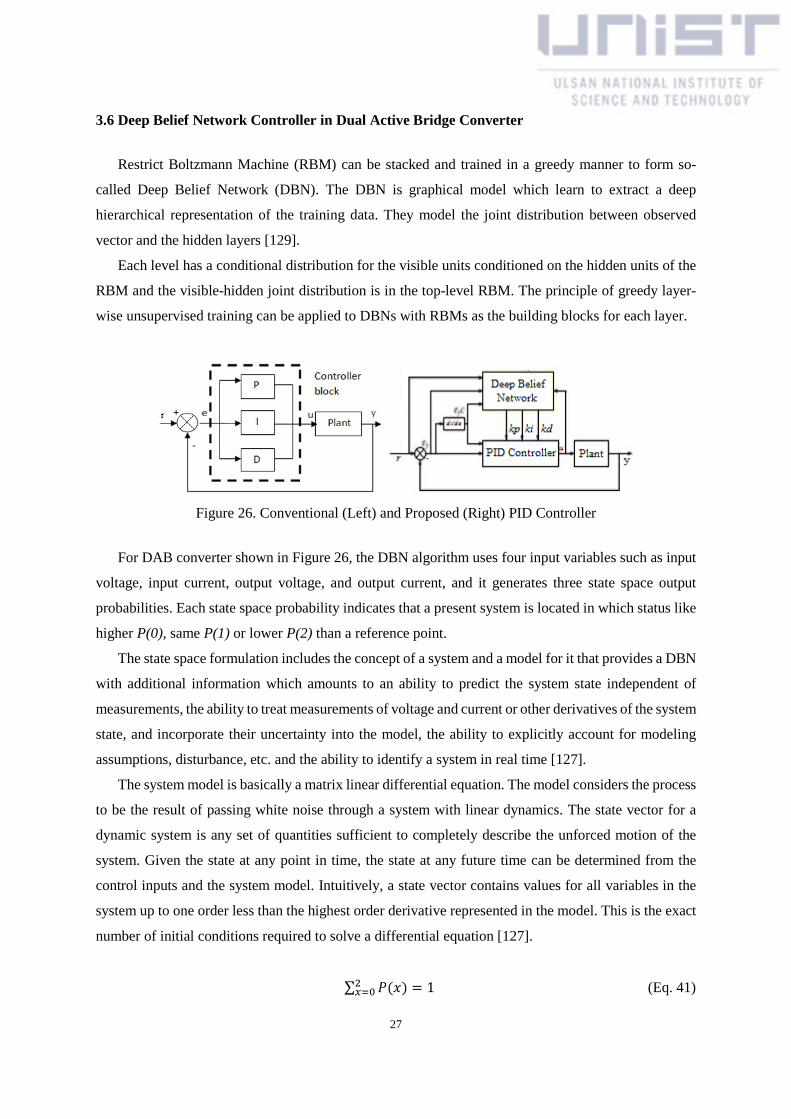
Figure 26. Conventional (Left) and Proposed (Right) PID Controller.............................................. 27
VII
Figure 27. Experimental Hardware Diagram .................................................................................... 30
Figure 28. Simulation Circuit Scheme with PSIM ............................................................................ 30
Figure 29. Picture of Experimental Hardware .................................................................................. 30
Figure 30. Diagram of PI-only Control ............................................................................................. 31
Figure 31. Design Digital Filter with Matlab .................................................................................... 32
Figure 32. Bode Plot (Kp, Ki) = (10, 10) .......................................................................................... 33
Figure 33. Proposed Algorithm Flow Chart ...................................................................................... 34
Figure 34. ADC Sampling Period, PWM Period and Computation Time Delay .............................. 34
Figure 35. Conventional (Top) and Proposed (Bottom) Simulation Waveform ............................... 35
Figure 36. Conventional (Top) and Proposed (Bottom) Full Load 3.3kW Waveform ..................... 36
Figure 37. Conventional (Left) and Proposed (Right) Waveform of Starting Point ......................... 37
Figure 38. Conventional (Left) and Proposed (Right) Waveform of Load Variation from 8.7A to 4.3A .................................................................................................................................. 37
Figure 39. Conventional (Left) and Proposed (Right) Waveform of Load Variation from 4.3A to 8.7A .................................................................................................................................. 37
Figure 40. Efficiency of Conventional (Left) and Proposed (Proposed) Full Load 3.3kW .............. 38
Figure 41. Efficiency of Experimental Hardware ............................................................................. 38
VIII

List of Tables
Table 1. Parameters of Ziegler Nichols Tuning Method ................................................................. 28
Table 2. Circuit Parameters of DAB Converter ............................................................................... 29
Table 3. Parameters of Digital Filter ............................................................................................... 31
Table 4. Parameters of DBN ............................................................................................................ 32
IX

I. Introduction
In order to reduce the dependency of non-renewable fossil fuel and the amount of greenhouse gas
emission, the demand for higher penetration of renewable energy has been growing rapidly during the
last two decades. The major sources of renewable energy include wind energy, photovoltaic energy,
hydrogen fuel cell energy, tidal energy, and geothermal energy. Most of these energy resources are
utilized in the form of electric energy resources and the higher penetration of renewable energy will
bring some challenges to the existing electric power system.
Figure 1. Centralized (Left) and Decentralized (Right) Energy Network System [123]
As shown in Figure 1, the existing electric power distribution system needs to be changed in order
to incorporate more renewable energy resources. The conventional power system includes large,
centralized power generators by burning gas, oil, or coal or by hydra-power, where power generation is
usually predictable and schedulable. Electric power is provided to consumers through passive
transformers, transmission lines, and substations. The flow of electric power is unidirectional from
generators to consumers. However, this paradigm is changed. Firstly, renewable power sources are
distributed and might be located near the end consumers such as roof-mounted solar panels or fuel cell
stations near a residential area. Furthermore, the direction of power flow is not always in one direction.
Consumers are able to produce electric energy to the grid. Secondly, renewable power sources are
usually not as schedulable and predictable as centralized power generators. Therefore, it is necessary
and preferable to install electric energy storage at the distribution level. Energy storage devices can be
in the forms of battery stations or the on-board batteries of plug-in hybrid vehicles.
The trends of power generation at the distribution level, bi-directional power flow, and energy
storage are similar to the transition from TV broadcasting to the computer network. In computer
networks, users are able to create, store, and exchange information by themselves. Similarly, the next
generation of power grid is referred as the “Energy Internet” [1], which includes energy router,
1

intelligent fault interrupting device, energy storage device, and the related control and communication
equipment.
“Energy Internet” is a prototype of the next generation of power systems with high penetration of
energy storage and generation at the distribution level. In “Energy Internet”, with the rapid development
of power electronic devices, it is possible to apply high frequency Pulse-Width Modulation (PWM)
converters as Solid State Transformers (SSTs) at the distribution level [2, 3, 4]. A SST is able to control
power flow, which is the “energy router”, one of the key enabling components in the future energy
system [1].
1.1 Solid State Transformers
Solid State Transformers (SSTs) are essentially high switching frequency power electronic
converters that have four functionalities. Firstly, it provides a galvanic isolation between the input and
the output of the converter. Secondly, it provides an active control of power flow in both directions.
Thirdly, it provides a compensation to disturbances in the power grid, such as variations of input voltage,
short-term sag or swell. Lastly, it provides ports or interfaces to connect with distributed power
generators or energy storage devices.
As shown in Figure 2, the main role of SSTs is that they acts as buffers among power grid, loads,
distributed energy sources, and energy storage devices [1]. By decoupling the load from the source, the
consumers would not see the disturbance at the grid side in terms that the disturbance is compensated
by the SSTs. At the same time, the power grid could not see the reactive power generated by loads,
compensated by SSTs. Therefore, the distribution system becomes more efficient and stable.
Additionally, SSTs act as buffers for renewable power sources and help reduce the impact of
unpredictable and un-schedulable fluctuations of renewable electric power sources on both power grids
and loads. By all these characteristics, there exists a number of candidate circuit configurations for SSTs.
Figure 2. The Applications of Smart Solid-State Transformers [124]
2
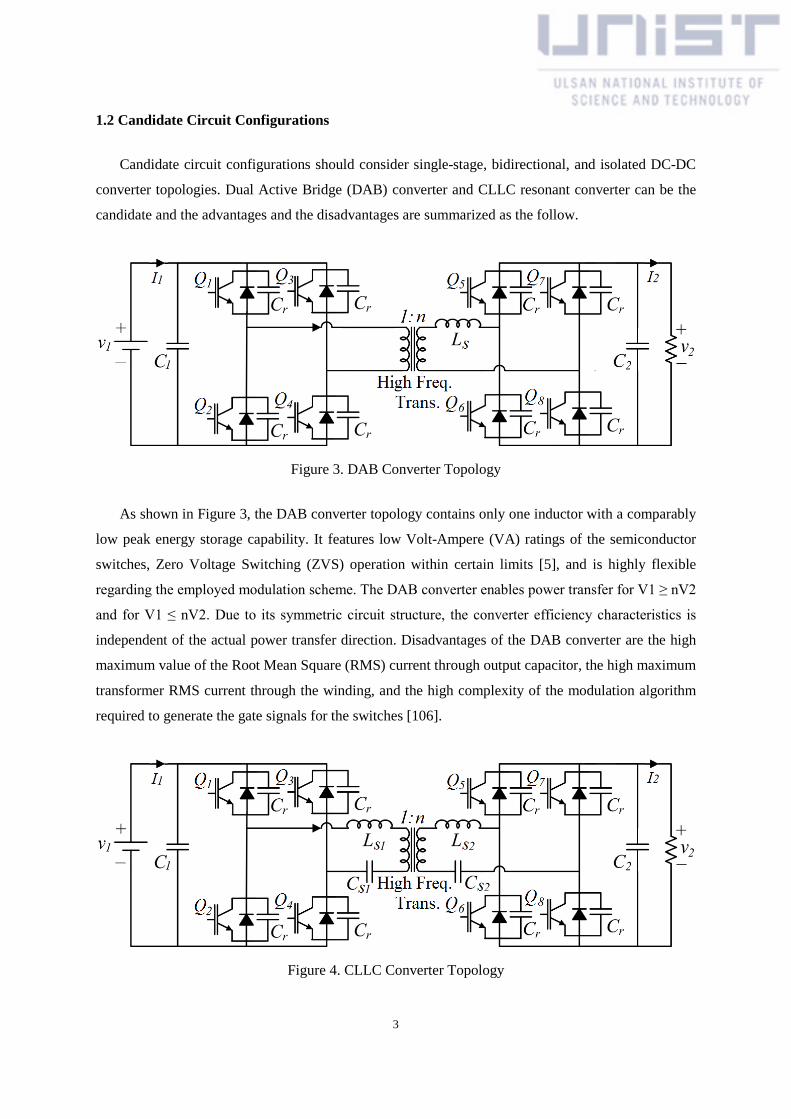
1.2 Candidate Circuit Configurations
Candidate circuit configurations should consider single-stage, bidirectional, and isolated DC-DC
converter topologies. Dual Active Bridge (DAB) converter and CLLC resonant converter can be the
candidate and the advantages and the disadvantages are summarized as the follow.
Figure 3. DAB Converter Topology
As shown in Figure 3, the DAB converter topology contains only one inductor with a comparably
low peak energy storage capability. It features low Volt-Ampere (VA) ratings of the semiconductor
switches, Zero Voltage Switching (ZVS) operation within certain limits [5], and is highly flexible
regarding the employed modulation scheme. The DAB converter enables power transfer for V1 ≥ nV2
and for V1 ≤ nV2. Due to its symmetric circuit structure, the converter efficiency characteristics is
independent of the actual power transfer direction. Disadvantages of the DAB converter are the high
maximum value of the Root Mean Square (RMS) current through output capacitor, the high maximum
transformer RMS current through the winding, and the high complexity of the modulation algorithm
required to generate the gate signals for the switches [106].
Figure 4. CLLC Converter Topology
3

As shown in Figure 4, CLLC resonant converter compared to the DAB converter, a slightly higher
average efficiency is calculated for the CLLC resonant converter. The semiconductor’s VA ratings are
similar. However, a larger value of the required magnetic storage capability occurs and an additional
resonance capacitor is needed for the resonant circuit. Thus, the resonant circuit of the CLLC resonant
converter requires a larger volume than the inductor of the DAB converter [6]. Again, a large RMS
current through output capacitor is calculated [106].
In contrast to the DAB converter, the electric energy stored in the resonance capacitor forces the
transformer current to change during the freewheeling time interval, which causes the transformer RMS
currents to increase. Thus, for converter operation according to Continuous Current Mode (CCM), the
CLLC resonant converter is more suitable if a variable switching frequency is permitted [106].
In addition, the efficiencies obtained with the DAB converter and the CLLC resonant converter are
very sensitive on the ratio of the input to output voltage. For V1/V2 < n or V1/V2 > n, large transformer
RMS currents occur and thus, large conduction losses result. This can be avoided in a two-stage
arrangement which keeps the input voltage of the isolated DC-DC converter closed to nV2 [106].
Based on these findings, the DAB converter topology is considered most promising with respect to
the achievable converter efficiency and the achievable power density due to the low number of
components and due to the employed capacitive filters [7], i.e. the DC capacitor is used instead of the
DC inductor [106].
In Summary, a DAB converter is a high-power, high-power-density, and high-efficiency power
converter with galvanic isolation [5]. It consists of two H-bridges of active power switching devices
and one high-frequency transformer. The high-frequency transformer provides both galvanic isolation
and energy storage in its winding leakage inductance. The two H-bridges operate at fixed 50% duty
ratio and the phase shift between the two bridges control the amount and direction of power flow.
1.3 Analysis and Applications of DAB Converters
Bidirectional isolated dc-dc DAB converters were initially proposed as candidates for high power
density and high power dc-dc converters [5]. The DAB topology is attractive because it has Zero-
Voltage Switching (ZVS), bidirectional power flow, and lower component stresses. A DAB converter
consists of two H-bridges and one high-frequency transformer. One H-bridge converts the input voltage
to an intermediate high-frequency ac voltage, while another H-bridge converts the high-frequency
square wave ac voltage back to the output voltage. A high-frequency transformer is used along with
high-frequency switching devices because it reduces the weight and volume of passive magnetic
devices. Beside galvanic isolation, the high-frequency transformer also has some leakage inductance in
its primary and secondary windings, which together act as an energy storage component. The leakage
inductance also helps achieve soft switching. During switching transients, transformer current resonates
4

with the capacitors in parallel with switching devices, limiting the dv/dt and di/dt across the switches.
Soft switching helps to reduce switching loss and achieve higher power efficiency.
Unlike other isolated dc-dc converters using asymmetrical topologies [8, 9, 10], DAB converters
have a symmetrical circuit configuration, which enables bidirectional power flow needed for SSTs. The
power flow of a DAB converter can be controlled by varying the phase shift between those two bridges.
Such phase shift changes the voltage across the transformer leakage inductance. In this way, the
direction of power flow and the amount of power transferred are controlled. Power is transferred from
the leading bridge to the lagging bridge.
DAB converters have become an interesting research area in recent years. Some researchers focus
on improvement of modulation methods. Dual phase-shift modulation has been proposed to reduce
reactive power and loss for DAB converters [11]. Hybrid modulation methods have been developed to
increase soft-switching range [12, 13]. Phase shift modulation plus duty-ratio control has been applied
to DAB converters to achieve higher degree of control freedom [14, 15, 16, 17, 18]. Different
modulation methods are evaluated and compared [19]. New switching strategies are presented to reduce
the switching loss and increase efficiency of DAB converters [11, 20]. More detailed circuit models are
developed and analyzed to address some parasitic and nonlinear effects of DAB converters [21, 22].
Some published works focus on efficiency evaluation of DAB converters [23, 24]. Several circuit design
optimizations are published [25, 26, 27, 28, 29, 30, 31]
The DAB dc-dc converter has been used in battery-application systems, such as uninterruptible
power supplies (UPS), battery management systems (BMS), and auxiliary power supplies for electric
vehicles or hybrid electrical vehicles. For instance, an off-line UPS design based on the DAB topology
is investigated [32]. DAB converters are applied to manage bidirectional energy transfer between an
energy storage system and a dc power system [25, 33, 34, 35]. DAB converters have been selected as a
key component for automotive applications [36, 37, 38, 39, 40, 41]. DAB converters are also identified
as the main circuit in the power electronic converter system between an ac power system and a
renewable power source [42, 43, 44, 45]. The topology of DAB converters has been extended to allow
multiple input/output ports [34, 46, 47, 48, 35]. The use of DAB converters in high power renewable
power generation is published [30].
1.4 Modeling of Power Converters
Good controller design requires good plant models [49]. A high switching frequency power
converter is essentially a nonlinear and time-varying system due to its switching nature. However, most
control methodologies prefer a linear and time-invariant plant. Therefore, various modeling techniques
have been proposed to approximate the nonlinearity and time-varying behaviors of a power converter
and to provide a linear and time-invariant approximation of the power converter of interest.
5

Figure 5. Actual Waveform and Averaged Waveform
As shown in Figure 5, one commonly used modeling technique is state-space averaging [50, 51, 52,
53]. This conventional technique assumes that the switching frequency is much higher than the
frequencies of interest and that the ripples in the state variables such as inductor current and capacitor
voltage are small enough. It approximates the matrix exponentials in the solution of the power converter
state equations using only linear and bi-linear terms, removes all quadratic terms, and results in a time-
invariant model. This model can be further linearized around a steady-state operating point and then a
linear, time-invariant small-signal model is derived. State-space averaging essentially takes the dc terms
in the Fourier series of state variables. There is another averaging technique called generalized state
space averaging, which keeps more terms in the Fourier series of state variables, normally the switching-
frequency terms [54, 55, 56, 57, 58, 59]. One advantage of generalized averaging is that it does not
assume that the ripples of state variables are small. This technique discards less information and might
be able to obtain more accurate models.
Besides generalized averaging, there is another averaging technique, called the Krylov-Bogoliubov-
Mitropolsky (KBM) averaging method [60, 61]. Instead of using Fourier series of state variables, the
KBM method approximates converter state variables by piecewise-polynomial equations. The effect of
ripples caused by switching is included in this way. The KBM method is simpler than generalized
averaging and does not require small ripples either. However, it might not be as useful as generalized
averaging is when modeling pure ac state variables.
The three modeling techniques discussed above are all in the continuous-time domain. On the other
hand, sampled-data models are in the discrete-time domain [53, 62, 63, 64, 65, 66]. A sampled-data
model uses the fact that state variables of power converters have cycle-by-cycle repeatable trajectories
in steady state. It is often derived by integrating the switched piecewise linear differential equations of
state variables over one control cycle. The integration is in fact solving the state equations given a set
of initial conditions, which involves multiplication and integration of exponentials and this process is
frequently approximated by Taylor series expansions.
The controller design for DAB converters, like other power converters, also requires an average
model of DAB converters. Currently there are two approaches to model a DAB converter in the
literature. Firstly, a simplified reduced-order model that neglects the transformer current dynamic [67,
68, 69] and secondly, a full-order discrete-time model that preserves the dynamic of transformer current 6

[70, 71]. Discrete-time modeling is one approach to model those converters with large variation and
resonant operations. However, a continuous-time model is usually preferred in terms that it provides
more physical insight and facilitates control design. The conventional state-space averaging technique
for dc-dc converters requires negligible current ripple [53]. However, this condition is not satisfied in
DAB converters because the transformer current of a DAB converter is purely ac. Instead, the
generalized averaging technique, which uses more terms in the Fourier series of state variables, is able
to capture the effect of pure ac current on converter dynamics [55, 57].
The rule-of-thumb for a dc-dc converter design is to separate the dynamics of current and voltage
by selecting proper converter parameters. The simplified reduced-order model addressed above assumes
that the dynamics of the transformer current are significantly faster than those of the output capacitor
voltage. However, this assumption has not been verified analytically. Singular perturbation theory
provides an analytical approach to separate the dynamics of different time-scales and provides the
conditions of separation of the dynamics [72, 73]. The criteria of time-scale separation of state variables
in dc-dc boost converters is reported [73].
1.5 Control of Power Converters
Figure 6. Comparison between Open and Closed Loop Control
As shown in Figure 6, a closed-loop controller is required when the output voltage of a power
converter needs to be regulated and source or load disturbances need to be compensated. The idea of
closed-loop control is essentially using the error between actual output and its reference to eliminate or
minimize the error. The conventional controller design method for power converters is as following
steps; firstly, derive the small-signal model around a steady-state operating point, secondly, find the
control-to-output transfer function of the converter, thirdly, specify the expected loop gain based on
7

design specifications, and at last, design the controller transfer function to match the desired loop gain
[53].
A Proportional-Integral (PI) controller is a commonly used controller for power converters which
require zero steady-state error as the reference is a dc signal. A lead and lag compensator is another
kind of controller for power converter that increases the phase-margin of the loop gain. One drawback
of both PI controller and lead compensator is that they only achieve infinite gain at dc, making it difficult
to obtain zero steady-state error if the reference or disturbance is a low-frequency ac signal.
The controllers mentioned above are essentially designed for one operating point. Large phase
margin and gain margin are necessary to ensure stable dynamic response when operating point deviates.
However, the dynamic performance is not guaranteed when there exists a large deviation of operating
point caused by significant disturbance. Gain-scheduling control is one method of improvement [74,
75, 76, 77]. A set of controllers are selected using the mentioned above methods for different operating
points. A supervisory controller switches among parameters depended on feedback information,
improving the performance over a wide operating range.
Adaptive control is a broader variant of gain-scheduling control. An adaptive controller adjusts its
control parameters dynamically [78]. On-line parameter adjustment is able to provide better
performance than the off-line adjustment in gain-scheduling control. Adaptive control is suitable for a
system where the structure is known while the parameters of the system are varying or unknown. For
instance, load resistance is treated as an unknown parameter [79] and better output voltage regulation
is achieved with an adaptive PI controller. Adaptive control has also been applied in active rectifiers
[80], inverters [81], and fuel cell power generation systems [82].
Beside the control design methods based on usually linear small-signal average model, there are
other nonlinear methods which use large signal models for controller design. One method is Lyapunov-
based back-stepping design. A positive-definite energy-like function, called a Lyapunov function, is
defined by the large signal converter average model. Control design is accomplished when the control
input is able to make the time derivative of the Lyapunov function negative-definite [83, 84, 85, 86].
The Lyapunov-based control technique has been applied to dc-dc converters [87], active-front-end
rectifiers [88], and voltage-source inverters [89]. Another nonlinear control method is sliding mode
control (SMC) [90]. SMC is a variable structure control method. It defines a set of control structures.
By switching between the control structures, the state variables are controlled to slide along a predefined
expected trajectory. The switching nature of SMC makes it suitable as a controller for power electronic
converters. SMC has been applied in the control of dc-dc converters [91, 92], ac-ac converters [93], and
doubly-fed inductor generators [94]. One advantage of nonlinear-based designs is that global stability
and performance are studied and can be analytically verified. Another advantage of such control
methods is the possibility of compensating for the non-minimum phase effect of boost-type converters
[95]. 8

Computational intelligence algorithms can also be applied for power converter controllers. Fuzzy
logic is a computational intelligence paradigm. Advantages of fuzzy logic control include ease of
implementation and resistance to disturbances [96]. Fuzzy logic has been used in adaptive energy
management for electric vehicles [97], grid-tie solar inverters [98], and active front-end rectifiers [99].
There are amount of literatures on the control of DAB converters. The state-of-the-art is using PI
controllers with some simplified assumptions on converter models [100, 101, 102, 103]. A relatively
large dc-link capacitor is used to reduce the voltage ripple caused by second order harmonic. When
several dc-dc DAB converters are connected in input-series-output-parallel configuration, instability
problems might happen when bus voltage and output power are not balanced. Therefore, some works
introduce voltage and balance control methods to solve such problems [104, 105].
9

II. Dual Active Bridge Converters
This section theoretically discusses the circuit configuration, steady state operation, and small-
signal model of DAB converters for SSTs.
2.1 Circuit Configuration
A DAB converter consists of two switching bridges and one high-frequency transformer. Each
switching bridge is made up of four high-frequency active controllable switching devices like
MOSFETs and IGBTs in an H-bridge connection. Such connection is similar to the one used in full-
bridge dc-dc converters. However, instead of using uncontrollable switching devices, such as diodes,
bridge in the other side of transformer, DAB converters use two active bridges formed by active
controllable devices. This is the reason that the name “Dual Active Bridge” is given.
A transformer is used to provide galvanic isolation between the input side and the output side of a
DAB converter. A high-frequency transformer is preferred to reduce the weight and volume of the
magnetic core. Compared to those converters using line-frequency transformers, DAB converters uses
more silicon devices which price is continuously going down while using less copper and smaller
magnetic core which price is continuously going down. Besides galvanic isolation, the high-frequency
transformer has some amounts of leakage inductance in its primary and secondary windings. The
leakage inductance has two purposes. Firstly, it is used as energy storage components in DAB
converters and secondly, it reduces the dv/dt across switching devices during transients, facilitates soft
switching, and reduces switching losses.
Figure 7. The Circuit Schematic of DAB Converter
As shown in Figure 7, the circuit schematic of a dc-dc DAB converter. In the schematic, power
MOSFETs can be used in place of IGBT-diode pairs. The IGBT-diode pairs can conduct current bi-
directionally, so does the channel of power MOSFETs. Therefore, the circuit is able to conduct 10

bidirectional current. Furthermore, DAB converters have symmetrical dual active H-bridge
configuration, which help achieve bidirectional power flow. Moreover resonant capacitors are
connected in parallel with each switch cell to enable soft switching.
The inherent symmetry of the power circuit in a DAB converter ensures bidirectional power flow.
Each bridge is controlled using two-level modulation, with fixed 50% duty ratio. A DAB converter uses
Phase-Shift Modulation (PSM) for controller. Both the direction and the amount of power flow is
regulated by controlling the phase shift between the H-bridges. Power flows from the leading bridge to
the lagging bridge. Two operating modes, corresponding to two directions of power flow of a DAB
converter, respectively, are given as the follow. In the left of Figure 8, positive power flow is defined
as power from the left to the right for the converter, while in the right of Figure 8, negative power flow
is defined as power from the right to the left.
Figure 8. Positive Power Flow (Left) and Negative Power Flow (Right) of DAB Converter
The amount of power transferred to the load is controlled by the phase shift angle between two
bridges and formulated theoretically as follow.
𝑃𝑃 = 𝑛𝑛𝑛𝑛1𝑛𝑛22𝑓𝑓𝑓𝑓𝑓𝑓𝑓𝑓
𝐷𝐷(1 − 𝐷𝐷) (Eq. 1)
Where V1 is the voltage of first bridge, V2 is the voltage of second bridge, n is the turn ratio of high
frequency transformer, D is the amount of phase shift between first and second bridges, fs is the
switching frequency and Ls is the leakage inductance of transformer.
Ideally, when the loss of a converter is insignificant, output power is equal to input power and it
can be possible to show that the voltage transfer ratio of a dc-dc DAB converter is determined by
transformer leakage inductance, phase shift between bridges, and switching frequency.
11

2.2 Dual Active Bridge Converter Model
In order to maximize power and minimize ripple, Pulse Width Modulation (PWM) duty is fixed as
50% [10]. Single Phase Shift Modulation (SPSM) is a simple method to control the amount and
direction of power flow by phase shift between the first and the second bridges. In this dissertation, the
effect of dead-time for protection from short of switches is ignored. In Figure 9, 10, 11, theoretical
waveform of current and voltages can be identified as load variances with nV1 > V2 condition.
Figure 9. Heavy Load Waveform
Figure 10. Medium Load Waveform
12

Figure 11. Light Load Waveform
In order to model a DAB converter, the variation of converter current and voltage have to be
analyzed. Each switching period has 6 different states and can be defined by voltage and current at each
state [28, 70].
Figure 12. Equivalent Circuit during t0 ~ t1 [126]
In Figure 12, switch Q1 and Q4 turn on, V1 and nV1 has a positive value. Switch Q6 and Q7 turn
on, but current flows on parasitic diode of Q6 and Q7. Therefore, the leakage inductor of high frequency
transformer has a negative current flow and the current on the inductor can be expressed as the following
equation. At t1, inductor current reaches to 0.
VLs = nV1 + V2 (Eq. 2)
13

Figure 13. Equivalent Circuit during t1 ~ t2 [126]
In Figure 13, switch Q1, Q4, Q6 and Q7 still turn on and inductor current increases a positive
direction. Unlike t0 ~ t1, current flows on switch Q6 and Q7. The total transition of current during t0 ~
t2 can be formulate and current at t2 is derived as the following expression.
∆𝐼𝐼𝑓𝑓𝑓𝑓 = 𝐷𝐷𝐷𝐷𝑓𝑓𝑓𝑓
(𝑉𝑉2 + 𝑛𝑛𝑉𝑉1) (Eq. 3)
𝑖𝑖(𝑡𝑡2) = 𝑖𝑖(𝑡𝑡0) + 𝐷𝐷𝐷𝐷𝑓𝑓𝑓𝑓𝑓𝑓
(𝑉𝑉2 + 𝑛𝑛𝑉𝑉1) (Eq. 4)
Figure 14. Equivalent Circuit during t2 ~ t3 [126]
In Figure 14, switch Q1 and Q4 remain turn on. Switch Q6 and Q7 turn off and switch Q5 and Q8
turn on. At this moment, current flows on diode D5 and D8, not on the switches. The total variation of
current during t2 ~ t3 can be shown as the follow and current will be defined.
∆𝐼𝐼𝑓𝑓𝑓𝑓 = (1−𝐷𝐷)𝐷𝐷𝑓𝑓𝑓𝑓
(𝑛𝑛𝑉𝑉1 − 𝑉𝑉2) (Eq. 5)
𝑖𝑖(𝑡𝑡3) = 𝑖𝑖(𝑡𝑡2) + (1−𝐷𝐷)𝐷𝐷𝑓𝑓𝑓𝑓𝑓𝑓
(𝑛𝑛𝑉𝑉1− 𝑉𝑉2) (Eq. 6)
14

Figure 15. The Equivalent Circuit during t3 ~ t4 [126]
In Figure 15, switch Q5 and Q8 still turn on. Switch Q1 and Q4 turn off and switch Q2 and Q3 turn
on. The current direction of leakage inductor is changed by switching and then current decrease
continuously. In the end, current reaches to 0 at t4.
Figure 16. The Equivalent Circuit during t4 ~ t5 [126]
In Figure 16, switch Q2, Q3, Q5 and Q8 turn on and current flows on switches. The variation of
current expresses as the following formula.
∆𝐼𝐼𝑓𝑓𝑓𝑓 = −𝐷𝐷𝐷𝐷𝑓𝑓𝑓𝑓𝑓𝑓
(𝑛𝑛𝑉𝑉1 + 𝑉𝑉2) (Eq. 7)
Figure 17. Equivalent Circuit during t5 ~t6 [126]
In Figure 17, switch Q2, Q3, Q6 and Q7 turn on and current flows on switch Q2, Q3 and parasitic
diodes of switches. The variation of current is as the follow.
∆𝐼𝐼𝑓𝑓𝑓𝑓 = − (1−𝐷𝐷)𝐷𝐷𝑓𝑓𝑓𝑓𝑓𝑓
(𝑛𝑛𝑉𝑉1 − 𝑉𝑉2) (Eq. 8)
15

With the above whole formula which define voltage and current at each state, it can be possible to
derive a state equation as current variation. The whole state can be divided by 4 periods according to
current variation and state equation can be derived for calculating an average model and a small-signal
model at each state period.
t0 ~ t2
⎣⎢⎢⎢⎡𝑑𝑑𝑑𝑑𝑓𝑓𝑑𝑑𝑑𝑑𝑑𝑑𝑑𝑑1𝑑𝑑𝑑𝑑𝑑𝑑𝑑𝑑2𝑑𝑑𝑑𝑑 ⎦⎥⎥⎥⎤
=
⎣⎢⎢⎢⎡0 −1
𝑓𝑓− 1
𝑓𝑓1𝐶𝐶1
− 1𝑟𝑟𝑓𝑓𝐶𝐶1
01𝐶𝐶1
0 − 1𝑅𝑅𝐶𝐶2⎦
⎥⎥⎥⎤�𝑖𝑖𝑖𝑖𝑉𝑉1𝑉𝑉2�+ �
0 01
𝑟𝑟𝑓𝑓𝐶𝐶10
0 1𝑅𝑅𝐶𝐶2
� � 𝑣𝑣𝑣𝑣𝑣𝑣𝑣𝑣𝑣𝑣� (Eq. 9)
t2 ~ t3
⎣⎢⎢⎢⎡𝑑𝑑𝑑𝑑𝑓𝑓𝑑𝑑𝑑𝑑𝑑𝑑𝑑𝑑1𝑑𝑑𝑑𝑑𝑑𝑑𝑑𝑑2𝑑𝑑𝑑𝑑 ⎦⎥⎥⎥⎤
=
⎣⎢⎢⎢⎡ 0 −1
𝑓𝑓1𝑓𝑓
1𝐶𝐶1
− 1𝑟𝑟𝑓𝑓𝐶𝐶1
0
− 1𝐶𝐶1
0 − 1𝑅𝑅𝐶𝐶2⎦
⎥⎥⎥⎤�𝑖𝑖𝑖𝑖𝑉𝑉1𝑉𝑉2�+ �
0 01
𝑟𝑟𝑓𝑓𝐶𝐶10
0 1𝑅𝑅𝐶𝐶2
� � 𝑣𝑣𝑣𝑣𝑣𝑣𝑣𝑣𝑣𝑣� (Eq. 10)
t3 ~ t5
⎣⎢⎢⎢⎡𝑑𝑑𝑑𝑑𝑓𝑓𝑑𝑑𝑑𝑑𝑑𝑑𝑑𝑑1𝑑𝑑𝑑𝑑𝑑𝑑𝑑𝑑2𝑑𝑑𝑑𝑑 ⎦⎥⎥⎥⎤
=
⎣⎢⎢⎢⎡0 −1
𝑓𝑓− 1
𝑓𝑓1𝐶𝐶1
− 1𝑟𝑟𝑓𝑓𝐶𝐶1
01𝐶𝐶1
0 − 1𝑅𝑅𝐶𝐶2⎦
⎥⎥⎥⎤�𝑖𝑖𝑖𝑖𝑉𝑉1𝑉𝑉2�+ �
0 01
𝑟𝑟𝑓𝑓𝐶𝐶10
0 1𝑅𝑅𝐶𝐶2
� � 𝑣𝑣𝑣𝑣𝑣𝑣𝑣𝑣𝑣𝑣� (Eq. 11)
t5 ~ t6
⎣⎢⎢⎢⎡𝑑𝑑𝑑𝑑𝑓𝑓𝑑𝑑𝑑𝑑𝑑𝑑𝑑𝑑1𝑑𝑑𝑑𝑑𝑑𝑑𝑑𝑑2𝑑𝑑𝑑𝑑 ⎦⎥⎥⎥⎤
=
⎣⎢⎢⎢⎡ 0 −1
𝑓𝑓− 1
𝑓𝑓1𝐶𝐶1
− 1𝑟𝑟𝑓𝑓𝐶𝐶1
0
− 1𝐶𝐶1
0 − 1𝑅𝑅𝐶𝐶2⎦
⎥⎥⎥⎤�𝑖𝑖𝑖𝑖𝑉𝑉1𝑉𝑉2�+ �
0 01
𝑟𝑟𝑓𝑓𝐶𝐶10
0 1𝑅𝑅𝐶𝐶2
� � 𝑣𝑣𝑣𝑣𝑣𝑣𝑣𝑣𝑣𝑣� (Eq. 12)
The current wave form and status of system periodically change and each state equation has a
similar form with ẋ = A(x) + B(u). For controller, a small-signal analysis is needed, so an average model
based on each state equation is calculated. The waveform is symmetry during a switching period, model
consider only 0 ~ Ts [49].
In general, an average model assume that current is not changed during fast respond [49]. However,
in this paper, current is not neglected for a bi-directional power analysis. At each state, an average model
is as the follow.
16

Current
L 𝑑𝑑𝑑𝑑𝐿𝐿𝑑𝑑𝑑𝑑
= �𝑣𝑣1 + 𝑣𝑣2 [0 𝐷𝐷𝐷𝐷𝑣𝑣]𝑣𝑣1 − 𝑣𝑣2 [𝐷𝐷𝐷𝐷𝑣𝑣 𝐷𝐷𝑣𝑣] (Eq. 13)
𝑑𝑑𝑑𝑑𝐿𝐿𝑑𝑑𝑑𝑑
= 𝑑𝑑1+𝑑𝑑2(2𝐷𝐷−1)𝑓𝑓
= 1𝑓𝑓𝑣𝑣1 + 2𝐷𝐷−1
𝑓𝑓𝑣𝑣2 (Eq. 14)
Input Voltage
C1 𝑑𝑑𝑑𝑑1𝑑𝑑𝑑𝑑
= �
𝑑𝑑𝑓𝑓𝑟𝑟𝑓𝑓− 𝑑𝑑1
𝑟𝑟𝑓𝑓− 𝑖𝑖𝑓𝑓 −
(1−2𝐷𝐷)𝑑𝑑2−𝑑𝑑14𝑓𝑓𝑓𝑓𝑓𝑓
[0 𝐷𝐷𝐷𝐷𝑣𝑣]𝑑𝑑𝑓𝑓𝑟𝑟𝑓𝑓− 𝑑𝑑1
𝑟𝑟𝑓𝑓− 𝑖𝑖𝑓𝑓 −
𝑑𝑑2−(1−2𝐷𝐷)𝑑𝑑14𝑓𝑓𝑓𝑓𝑓𝑓
[𝐷𝐷𝐷𝐷𝑣𝑣 𝐷𝐷𝑣𝑣] (Eq. 15)
C1 𝑑𝑑𝑑𝑑1𝑑𝑑𝑑𝑑
= −𝑖𝑖𝑓𝑓 + �− 1𝑟𝑟𝑓𝑓
+ 2𝐷𝐷2−2𝐷𝐷+14𝑓𝑓𝑓𝑓𝑓𝑓
� 𝑣𝑣1 + 2𝐷𝐷2−14𝑓𝑓𝑓𝑓𝑓𝑓
𝑣𝑣2 + 𝑑𝑑𝑓𝑓𝑟𝑟𝑓𝑓
(Eq. 16)
Output Voltage
C2 𝑑𝑑𝑑𝑑2𝑑𝑑𝑑𝑑
= �−𝑖𝑖𝑓𝑓 −
(1−2𝐷𝐷)𝑑𝑑2−𝑑𝑑14𝑓𝑓𝑓𝑓𝑓𝑓
− 𝑑𝑑2𝑅𝑅− 𝑑𝑑𝑑𝑑𝑣𝑣
𝑅𝑅 [0 𝐷𝐷𝐷𝐷𝑣𝑣]
−𝑖𝑖𝑓𝑓 −𝑑𝑑2−(1−2𝐷𝐷)𝑑𝑑1
4𝑓𝑓𝑓𝑓𝑓𝑓− 𝑑𝑑2
𝑅𝑅− 𝑑𝑑𝑑𝑑𝑣𝑣
𝑅𝑅 [𝐷𝐷𝐷𝐷𝑣𝑣 𝐷𝐷𝑣𝑣]
(Eq. 17)
C2 𝑑𝑑𝑑𝑑2𝑑𝑑𝑑𝑑
= −𝑖𝑖𝑓𝑓 + �2𝐷𝐷2−2𝐷𝐷+14𝑓𝑓𝑓𝑓𝑓𝑓
� 𝑣𝑣1 + �2𝐷𝐷2−1
4𝑓𝑓𝑓𝑓𝑓𝑓− 1
𝑅𝑅� 𝑣𝑣2 + 𝑑𝑑𝑑𝑑𝑣𝑣
𝑅𝑅 (Eq. 18)
Therefore the formula of average model can be expressed as the following linear equation.
⎣⎢⎢⎢⎡𝑑𝑑𝑑𝑑𝐿𝐿𝑑𝑑𝑑𝑑𝑑𝑑𝑑𝑑1𝑑𝑑𝑑𝑑𝑑𝑑𝑑𝑑2𝑑𝑑𝑑𝑑 ⎦⎥⎥⎥⎤
=
⎣⎢⎢⎢⎡ 0 1
𝑓𝑓2𝐷𝐷−1𝑓𝑓
− 1𝐶𝐶1
− 1𝑟𝑟𝑓𝑓𝐶𝐶1
+ 2𝐷𝐷2−2𝐷𝐷+14𝑓𝑓𝑓𝑓𝑓𝑓𝐶𝐶1
2𝐷𝐷2−14𝑓𝑓𝑓𝑓𝑓𝑓𝐶𝐶1
− 1𝐶𝐶2
2𝐷𝐷2−2𝐷𝐷+14𝑓𝑓𝑓𝑓𝑓𝑓𝐶𝐶2
2𝐷𝐷2−14𝑓𝑓𝑓𝑓𝑓𝑓𝐶𝐶2
− 1𝑅𝑅𝐶𝐶2⎦
⎥⎥⎥⎤
�𝑖𝑖𝑓𝑓𝑣𝑣1𝑣𝑣2�+ �
0 01
𝑟𝑟𝑓𝑓𝐶𝐶10
0 1𝑅𝑅𝐶𝐶2
� � 𝑣𝑣𝑣𝑣𝑣𝑣𝑣𝑣𝑣𝑣� (Eq. 19)
The average model is appropriate for a real system in time domain, but it has a non-linearity.
Therefore, the model has to be linearized using small-signal model. The average model is divided into
dc and ac component as the follow.
𝑖𝑖𝑓𝑓(𝑡𝑡) = 𝐼𝐼𝑓𝑓 + 𝚤𝚤̃(𝑡𝑡) (Eq. 20)
𝑣𝑣1(𝑡𝑡) = 𝑉𝑉1 + 𝑣𝑣1�(𝑡𝑡) (Eq. 21)
𝑣𝑣2(𝑡𝑡) = 𝑉𝑉2 + 𝑣𝑣2�(𝑡𝑡) (Eq. 22)
𝑣𝑣𝑣𝑣(𝑡𝑡) = 𝑉𝑉𝑣𝑣 + 𝑣𝑣𝑣𝑣�(𝑡𝑡) (Eq. 23)
𝑣𝑣𝑣𝑣𝑣𝑣(𝑡𝑡) = 𝑉𝑉𝑣𝑣𝑣𝑣 + 𝑣𝑣𝑣𝑣𝑣𝑣� (𝑡𝑡) (Eq. 24)
𝑣𝑣(𝑡𝑡) = 𝐷𝐷 + �̃�𝑣(𝑡𝑡) (Eq. 25)
Defined variables insert to the average model, then the model expresses as the follow.
17

𝑑𝑑(𝐼𝐼𝐿𝐿+𝚤𝚤𝐿𝐿� )𝑑𝑑𝑑𝑑
= 1𝑓𝑓�𝑉𝑉1 + 𝑣𝑣1�� + 2�𝐷𝐷+𝑑𝑑��−1
𝑓𝑓(𝑉𝑉2 + 𝑣𝑣2�) (Eq. 26)
𝑑𝑑(𝑛𝑛1+𝑑𝑑1�)𝑑𝑑𝑑𝑑
= − 1𝐶𝐶1
(𝐼𝐼𝑓𝑓 + 𝚤𝚤̃) + �− 1𝑟𝑟𝑓𝑓𝐶𝐶1
+ 2�𝐷𝐷+𝑑𝑑��2−2�𝐷𝐷+𝑑𝑑��+14𝑓𝑓𝑓𝑓𝑓𝑓𝐶𝐶1
� �𝑉𝑉1 + 𝑣𝑣1�� + 2(𝐷𝐷+𝑑𝑑�)2−14𝑓𝑓𝑓𝑓𝑓𝑓𝐶𝐶1
�𝑉𝑉2 + 𝑣𝑣2�� +
1𝑟𝑟𝑓𝑓𝐶𝐶1
(𝑉𝑉𝑣𝑣 + 𝑣𝑣𝑣𝑣�) (Eq. 27)
𝑑𝑑(𝑛𝑛2+𝑑𝑑2�)𝑑𝑑𝑑𝑑
= − 1𝐶𝐶2
(𝐼𝐼𝑓𝑓 + 𝚤𝚤̃) + �2�𝐷𝐷+𝑑𝑑��2−2�𝐷𝐷+𝑑𝑑��+14𝑓𝑓𝑓𝑓𝑓𝑓𝐶𝐶2
� �𝑉𝑉1 + 𝑣𝑣1�� + �2(𝐷𝐷+𝑑𝑑�)2−14𝑓𝑓𝑓𝑓𝑓𝑓𝐶𝐶2
− 1𝑅𝑅𝐶𝐶2
� �𝑉𝑉2 + 𝑣𝑣2�� +
1𝑅𝑅𝐶𝐶2
(𝑉𝑉𝑣𝑣𝑣𝑣 + 𝑣𝑣𝑣𝑣𝑣𝑣� ) (Eq. 28)
The above formula divide into dc, first order and high order component. At last, only first order
component considers and the others remove, then it can be described as the following.
𝑑𝑑𝚤𝚤𝐿𝐿�𝑑𝑑𝑑𝑑
= 1𝑓𝑓𝑣𝑣1� + 2𝐷𝐷−1
𝑓𝑓𝑣𝑣2� + 2
𝑓𝑓𝑉𝑉2�̃�𝑣 (Eq. 29)
𝑑𝑑𝑑𝑑1�𝑑𝑑𝑑𝑑
= − 1𝐶𝐶1𝚤𝚤̃ + �− 1
𝑟𝑟𝑓𝑓𝐶𝐶1+ 2𝐷𝐷2−2𝐷𝐷+1
4𝑓𝑓𝑓𝑓𝑓𝑓𝐶𝐶1� 𝑣𝑣1� + 2𝐷𝐷2−1
4𝑓𝑓𝑓𝑓𝑓𝑓𝐶𝐶1𝑣𝑣2� + � 4𝐷𝐷−2
4𝑓𝑓𝑓𝑓𝑓𝑓𝐶𝐶1𝑉𝑉1 + 4𝐷𝐷
4𝑓𝑓𝑓𝑓𝑓𝑓𝐶𝐶1𝑉𝑉2� 𝑣𝑣 � + 1
𝑟𝑟𝑓𝑓𝐶𝐶1𝑣𝑣𝑣𝑣� (Eq. 30)
𝑑𝑑𝑑𝑑2�𝑑𝑑𝑑𝑑
= − 1𝐶𝐶2𝚤𝚤̃ + �2𝐷𝐷
2−2𝐷𝐷+14𝑓𝑓𝑓𝑓𝑓𝑓𝐶𝐶2
� 𝑣𝑣1� + �2𝐷𝐷2−1
4𝑓𝑓𝑓𝑓𝑓𝑓𝐶𝐶2− 1
𝑅𝑅𝐶𝐶2� 𝑣𝑣2� + � 4𝐷𝐷−2
4𝑓𝑓𝑓𝑓𝑓𝑓𝐶𝐶2𝑉𝑉1 + 4𝐷𝐷
4𝑓𝑓𝑓𝑓𝑓𝑓𝐶𝐶2𝑉𝑉2�𝑣𝑣 � + 1
𝑅𝑅𝐶𝐶2𝑣𝑣𝑣𝑣𝑣𝑣� (Eq. 31)
Above the equations organize as the following.
⎣⎢⎢⎢⎢⎡𝑣𝑣𝑖𝑖𝑓𝑓𝑣𝑣𝑡𝑡𝑣𝑣𝑣𝑣1𝑣𝑣𝑡𝑡𝑣𝑣𝑣𝑣2𝑣𝑣𝑡𝑡 ⎦
⎥⎥⎥⎥⎤
=
⎣⎢⎢⎢⎢⎢⎡ 0
1𝑖𝑖
2𝐷𝐷 − 1𝑖𝑖
−1𝐶𝐶1
−1
𝑟𝑟𝑣𝑣𝐶𝐶1+
2𝐷𝐷2 − 2𝐷𝐷 + 14𝑓𝑓𝑣𝑣𝑖𝑖𝐶𝐶1
2𝐷𝐷2 − 14𝑓𝑓𝑣𝑣𝑖𝑖𝐶𝐶1
−1𝐶𝐶2
2𝐷𝐷2 − 2𝐷𝐷 + 14𝑓𝑓𝑣𝑣𝑖𝑖𝐶𝐶2
2𝐷𝐷2 − 14𝑓𝑓𝑣𝑣𝑖𝑖𝐶𝐶2
−1𝑅𝑅𝐶𝐶2⎦
⎥⎥⎥⎥⎥⎤
�𝑖𝑖𝑓𝑓𝑣𝑣1𝑣𝑣2�
+
⎣⎢⎢⎢⎡ 0 2
𝑓𝑓𝑉𝑉2 0
1𝑟𝑟𝑓𝑓𝐶𝐶1
4𝐷𝐷−24𝑓𝑓𝑓𝑓𝑓𝑓𝐶𝐶1
𝑉𝑉1 + 4𝐷𝐷4𝑓𝑓𝑓𝑓𝑓𝑓𝐶𝐶1
𝑉𝑉2 0
0 4𝐷𝐷−24𝑓𝑓𝑓𝑓𝑓𝑓𝐶𝐶2
𝑉𝑉1 + 4𝐷𝐷4𝑓𝑓𝑓𝑓𝑓𝑓𝐶𝐶2
𝑉𝑉2 1𝑅𝑅𝐶𝐶2⎦
⎥⎥⎥⎤�𝑣𝑣𝑣𝑣��̃�𝑣𝑣𝑣𝑣𝑣𝑣𝑣�
� (Eq. 32)
The transfer function of system is possible to acquire using small-signal model as the follow [49].
[𝚤𝚤𝑓𝑓� ] = [1 0 0] �𝚤𝚤𝑓𝑓�𝑣𝑣1�𝑣𝑣2��
𝚤𝚤𝑓𝑓� = C(sI− A)−1𝐵𝐵𝐵𝐵(𝑡𝑡) = 𝐺𝐺11(𝑣𝑣)𝑣𝑣𝑣𝑣�(𝑣𝑣) + 𝐺𝐺12(𝑣𝑣)�̃�𝑣(𝑣𝑣) + 𝐺𝐺13(s)𝚤𝚤𝑜𝑜�(𝑣𝑣) (Eq. 33)
[𝚤𝚤𝑓𝑓� ] = [0 1 0] �𝚤𝚤𝑓𝑓�𝑣𝑣1�𝑣𝑣2��
𝚤𝚤𝑓𝑓� = C(sI− A)−1𝐵𝐵𝐵𝐵(𝑡𝑡) = 𝐺𝐺21(𝑣𝑣)𝑣𝑣𝑣𝑣�(𝑣𝑣) + 𝐺𝐺22(𝑣𝑣)�̃�𝑣(𝑣𝑣) + 𝐺𝐺23(s)𝚤𝚤𝑜𝑜�(𝑣𝑣) (Eq. 34) 18

[𝚤𝚤𝑓𝑓� ] = [0 0 1] �𝚤𝚤𝑓𝑓�𝑣𝑣1�𝑣𝑣2��
𝚤𝚤𝑓𝑓� = C(sI− A)−1𝐵𝐵𝐵𝐵(𝑡𝑡) = 𝐺𝐺31(𝑣𝑣)𝑣𝑣𝑣𝑣�(𝑣𝑣) + 𝐺𝐺32(𝑣𝑣)�̃�𝑣(𝑣𝑣) + 𝐺𝐺33(s)𝚤𝚤𝑜𝑜�(𝑣𝑣) (Eq. 35)
The small-signal schematic of a closed loop feedback control system that consists of a DAB
converter is shown as Figure 18. Note that a delay term esTd is added to the feedback loop to represent
the sampling and processing delay Td, which is caused by the digital implementation of the control
algorithm and modulation processes.
Figure 18. Small-Signal Schematic of Closed-loop Controlled DAB
19

III. Deep Belief Network Controller
In recent years, there’s been a resurgence in the field of Artificial Intelligence. It’s spread beyond
the academic world with major players like Google, Microsoft, and Facebook creating their own
research teams and making some impressive acquisitions.
Some of this can be attributed to the abundance of raw data generated by social network users, much
of which needs to be analyzed, as well as to the cheap computational power available via General
Purpose Graphic Processing Units (GPGPUs). But beyond these phenomena, this resurgence has been
powered in no small part by a new trend in AI, specifically in machine learning, known as Deep
Learning.
3.1 Perceptrons
One of the earliest supervised training algorithms is that of the perceptron, a basic neural network
building block. For example, there are n points in the plane, labeled ‘0’ and ‘1’. Then, a new point is
given and guess its label. One approach might be to look at the closest neighbor and return that point’s
label. But a slightly more intelligent way of going about it would be to pick a line that best separates
the labeled data and use that as classifier.
Figure 19. Linear Classifier Example
In this case, each piece of input data would be represented as a vector x = (x1, x2) and function
would be something like ‘0’ if below the line, ‘1’ as shown in Figure 19. To represent this
mathematically, let separator be defined by a vector of weights w and a vertical offset or bias b. Then,
our function would combine the inputs and weights with a weighted sum transfer function. 20

𝑓𝑓(𝑥𝑥) = 𝑥𝑥 · 𝑤𝑤 + 𝑏𝑏 (Eq. 36)
Then, the result of this transfer function would be fed into an activation function to produce a
labeling. In the example above, activation function was a threshold cutoff (e.g., 1 if greater than some
value).
ℎ(𝑥𝑥) = � 1, 𝑖𝑖𝑓𝑓 𝑓𝑓(𝑥𝑥) = 𝑤𝑤 · 𝑥𝑥 + 𝑏𝑏 > 0 0, 𝑜𝑜𝑡𝑡ℎ𝑒𝑒𝑟𝑟𝑤𝑤𝑖𝑖𝑣𝑣𝑒𝑒 (Eq. 37)
The training of the perceptron consists of feeding it multiple training samples and calculating the
output for each of them. After each sample, the weights w are adjusted in such a way so as to minimize
the output error, defined as the difference between the desired target and the actual outputs. There are
other error functions, like the mean square error, but the basic principle of training remains the same.
The single perceptron has one major drawback as shown in Figure 20. It can only learn linearly
separable functions. For example, take XOR, a relatively simple function, and notice that it cannot be
classified by a linear separator.
Figure 20. XOR Problem Example
To address this problem, using a multilayer perceptron is needed, also known as feed-forward neural
network. In effect, it will create a more powerful mechanism for learning to compose a bunch of these
perceptrons together.
3.2 Feed-forward Networks
A neural network is just a composition of perceptrons, connected in different ways and operating
on different activation functions.
21

Figure 21. Feed-forward Network
The feed-forward neural network is shown in Figure 21, which has the following properties. An
input, output, and one or more hidden layers. The figure above shows a network with a 3-unit input
layer, 4-unit hidden layer and an output layer with 2 units. Each unit is a single perceptron like the one
described above. The units of the input layer serve as inputs for the units of the hidden layer, while the
hidden layer units are inputs to the output layer. Each connection between two neurons has a weight w
similar to the perceptron weights. Each unit of layer t is typically connected to every unit of the previous
layer t-1 although setting their weight to 0 disconnect them.
To process input data, clamping the input vector to the input layer, setting the values of the vector
as outputs for each of the input units. In this particular case, the network can process a 3-dimensional
input vector because of the 3 input units. For example, if input vector is (7, 1, 2), then set the output of
the top input unit to 7, the middle unit to 1, and so on. These values are then propagated forward to the
hidden units using the weighted sum transfer function for each hidden unit, hence the term forward
propagation, which in turn calculate their outputs activation function. The output layer calculates it’s
outputs in the same way as the hidden layer. The result of the output layer is the output of the network.
If each of our perceptrons is only allowed to use a linear activation function, then the final output
of our network will still be some linear function of the inputs, just adjusted with a ton of different
weights that it’s collected throughout the network. In other words, a linear composition of a bunch of
linear functions is still just a linear function. A linear composition of a bunch of linear functions is still
just a linear function, so most neural networks use non-linear activation functions. Because of this, most
neural networks use non-linear activation functions like the logistic, tanh, binary or rectifier. Without
them the network can only learn functions which are linear combinations of its inputs.
The hidden layer is of particular interest. By the universal approximation theorem, a single hidden
layer network with a finite number of neurons can be trained to approximate an arbitrarily random
function. In other words, a single hidden layer is powerful enough to learn any function. Learning is
often better in practice with multiple hidden layers (i.e., deeper nets).
22

The hidden layer is where the network stores its internal abstract representation of the training data,
similar to the way that a human brain, greatly simplified analogy, has an internal representation of the
real world.
A neural network is able to have more than one hidden layer. In that case, the higher layers are
building new abstractions on top of previous layers and learning is often better in-practice with larger
networks. However, increasing the number of hidden layers leads to two known issues [122].
Firstly, vanishing gradients. As adding more and more hidden layers, back-propagation becomes
less and less useful in passing information to the lower layers. In effect, as information is passed back,
the gradients begin to vanish and become small relative to the weights of the networks.
Secondly, overfitting. Perhaps the main problem in Machine Learning. Briefly, over-fitting
describes the phenomenon of fitting the training data too closely, maybe with hypotheses that are too
complex. In such a case, learner ends up fitting the training data really well, but will perform much
more poorly on real examples.
3.3 Training
The most common algorithm for supervised training of the multilayer perceptrons is known as back-
propagation. The basic procedure is as the follow. A training sample is presented and propagated
forward through the network. The output error is calculated, typically the Mean Squared Error (MSE).
𝐸𝐸 = 12
(𝑡𝑡 − 𝑦𝑦)2 (Eq. 38)
Where t is the target value and y is the actual network output. Other error calculations are also
acceptable, but the MSE is a good choice. Network error is minimized using a method called stochastic
gradient descent [117].
Figure 22. Global and Local Optimization Problem
23

As shown in Figure 22, gradient descent is universal, but in the case of neural networks, this would
be a graph of the training error as a function of the input parameters. The optimal value for each weight
is that at which the error achieves a global minimum. During the training phase, the weights are updated
in small steps, after each training sample or a mini-batch of several samples, in such a way that they are
always trying to reach the global minimum, but this is no easy task, as you often end up in local minima,
like the one on the right. For example, if the weight has a value of 0.6, it needs to be changed towards
0.4.
This, Figure 22, represents the simplest case, that in which error depends on a single parameter.
However, network error depends on every network weight and the error function is much more complex.
Thankfully, back-propagation provides a method for updating each weight between two neurons with
respect to the output error. The derivation itself is quite complicated, but the weight update for a given
node has the following simple form.
𝛥𝛥𝑤𝑤𝑑𝑑 = −α ∂𝐸𝐸∂𝑤𝑤𝑖𝑖
(Eq. 39)
Where E is the output error, and wi is the weight of input i to the neuron.
Essentially, the goal is to move in the direction of the gradient with respect to weight i. The key
term is the derivative of the error, which is not always easy to calculate. The method of finding this
derivative for a random weight of a random hidden node in the middle of a large network is through
back-propagation. The errors are first calculated at the output units where the formula is quite simple,
based on the difference between the target and predicted values, and then propagated back through the
network in a clever fashion, allowing to efficiently update weights during training and hopefully reach
a minimum.
3.4 Restricted Boltzmann Machines
Restricted Boltzmann machines (RBM) are a generative stochastic neural network that can learn a
probability distribution over its set of inputs [116].
Figure 23. Interaction between Visible Layer and Hidden Layer in DBN [109]
24

Shown as Figure 23, RBMs are composed of a hidden, visible, and bias layer. Unlike the feed-
forward networks, the connections between the visible and hidden layers are undirected, the values can
be propagated in both the visible-to-hidden and hidden-to-visible directions, and fully connected, each
unit from a given layer is connected to each unit in the next. If any unit in any layer allow to connect to
any other layer, then we would have a Boltzmann machine rather than RBM.
The standard RBM has binary hidden and visible units. That is, the unit activation is 0 or 1 under a
Bernoulli distribution, but there are variants with other non-linearities.
3.4 Contrastive Divergence
Figure 24. Contrastive Divergence Example [125]
As shown in Figure 24, the single-step contrastive divergence algorithm (CD-1) works as follow.
Firstly, positive phase consists that an input sample v is clamped to the input layer and v is
propagated to the hidden layer in a similar manner to the feed-forward networks. The result of the
hidden layer activations is h.
Secondly, negative phase consists propagate h back to the visible layer with result v’, the
connections between the visible and hidden layers are undirected and thus allow movement in both
directions, and propagate the new v’ back to the hidden layer with activations result h’.
At last, weight update
𝑤𝑤(𝑡𝑡 + 1) = 𝑤𝑤(𝑡𝑡) + 𝑎𝑎(𝑣𝑣ℎ𝐷𝐷 − 𝑣𝑣′ℎ′𝐷𝐷) (Eq. 40)
Where a is the learning rate and v, v’, h, h’, and w are vectors.
The intuition behind the algorithm is that the positive phase, which is h given v, reflects the
network’s internal representation of the real world data. Meanwhile, the negative phase represents an
attempt to recreate the data based on this internal representation, which is v’ given h. The main goal is
for the generated data to be as close as possible to the real world and this is reflected in the weight
update formula [119, 120, 121].
25

In other words, the net has some perception of how the input data can be represented, so it tries to
reproduce the data based on this perception. If its reproduction is not close enough to reality, it makes
an adjustment and tries again.
3.5 Deep Belief Networks
The hidden layers of RBMs act as effective feature detectors; but it’s rare to use these features
directly. In fact, the data set above is more an exception than a rule. Instead, we need to find some way
to use these detected features indirectly [116].
Luckily, it was discovered that these structures can be stacked to form deep networks. These
networks can be trained greedily, one layer at a time, to help to overcome the vanishing gradient and
over-fitting problems associated with classic back-propagation. The resulting structures are often quite
powerful, producing impressive results [113, 122].
Boltzmann machines stack to create a class known as deep belief networks (DBNs).
Figure 25. Example of Training RBM for Predicting y [108]
In Figure 25, the hidden layer of RBM t acts as a visible layer for RBM t+1. The input layer of the
first RBM is the input layer for the whole network, and the greedy layer-wise pre-training works as the
follows. Firstly, train the first RBM t=1 using contrastive divergence with all the training samples.
Secondly, train the second RBM t=2. Since the visible layer for t=2 is the hidden layer of t=1, training
begins by clamping the input sample to the visible layer of t=1, which is propagated forward to the
hidden layer of t=1. This data then serves to initiate contrastive divergence training for t=2. Thirdly,
repeat the previous procedure for all the layers. At last, after pre-training the network can be extended
by connecting one or more fully connected layers to the final RBM hidden layer. This forms a multi-
layer perceptron which can then be fine-tuned using back-propagation.
26
3.6 Deep Belief Network Controller in Dual Active Bridge Converter
Restrict Boltzmann Machine (RBM) can be stacked and trained in a greedy manner to form so-
called Deep Belief Network (DBN). The DBN is graphical model which learn to extract a deep
hierarchical representation of the training data. They model the joint distribution between observed
vector and the hidden layers [129].
Each level has a conditional distribution for the visible units conditioned on the hidden units of the
RBM and the visible-hidden joint distribution is in the top-level RBM. The principle of greedy layer-
wise unsupervised training can be applied to DBNs with RBMs as the building blocks for each layer.
Figure 26. Conventional (Left) and Proposed (Right) PID Controller
For DAB converter shown in Figure 26, the DBN algorithm uses four input variables such as input
voltage, input current, output voltage, and output current, and it generates three state space output
probabilities. Each state space probability indicates that a present system is located in which status like
higher P(0), same P(1) or lower P(2) than a reference point.
The state space formulation includes the concept of a system and a model for it that provides a DBN
with additional information which amounts to an ability to predict the system state independent of
measurements, the ability to treat measurements of voltage and current or other derivatives of the system
state, and incorporate their uncertainty into the model, the ability to explicitly account for modeling
assumptions, disturbance, etc. and the ability to identify a system in real time [127].
The system model is basically a matrix linear differential equation. The model considers the process
to be the result of passing white noise through a system with linear dynamics. The state vector for a
dynamic system is any set of quantities sufficient to completely describe the unforced motion of the
system. Given the state at any point in time, the state at any future time can be determined from the
control inputs and the system model. Intuitively, a state vector contains values for all variables in the
system up to one order less than the highest order derivative represented in the model. This is the exact
number of initial conditions required to solve a differential equation [127].
∑ 𝑃𝑃(𝑥𝑥)2𝑥𝑥=0 = 1 (Eq. 41)
27

Using these probabilities, algorithm can calculate Ku which is the ultimate value for adjusting gain
variables. At the end, each gain of the PID controller updates new gain value after Ku.
𝐾𝐾𝑢𝑢 = ∑ (𝑥𝑥 − 1) 𝑃𝑃(𝑥𝑥)2𝑥𝑥=0 (Eq. 42)
∆𝐾𝐾𝑝𝑝 = 𝑤𝑤𝑝𝑝𝐾𝐾𝑢𝑢 (Eq. 43)
∆𝐾𝐾𝑑𝑑 = 𝑤𝑤𝑑𝑑𝐾𝐾𝑢𝑢 (Eq. 44)
∆𝐾𝐾𝑑𝑑 = 𝑤𝑤𝑑𝑑𝐾𝐾𝑢𝑢 (Eq. 45)
Weight wp, wi, and wd are variables for adjusting each gain parameter from Ku which is calculated
by algorithm. As shown in Table 1, they can be acquired by adapting some values from Ziegler-Nichols
tuning method which is a heuristic method of tuning a PID controller [110].
Table 1. Parameters of Ziegler Nichols Tuning Method Type of
Controller
Controller Parameters
Kp Ki Kd
P 0.5 Ku - -
PI 0.45 Ku 1.2 Kp/Tu -
PD 0.8 Ku - KpTu/8
PID 0.6 Ku 2Kp/Tu KpTu/8
It is performed by setting the integral and derivative gains to zero. Kp is a proportional gain, Ku is
a ultimate gain at which the output of the control loop oscillates with a constant amplitude and Tu is a
oscillation period.
28

IV. Simulation and Experiment
Simulation is conducted with PSIM 9.3 and Matlab 2013a. Experiment is conducted with Code
Composer Studio 5.4 and TMS320F28335 digital signal process unit made by Texas Instruments.
4.1 Circuit Configuration
Simulation and experiment results are provided in order to verify the proposed model analysis and
control theory. The main parameters for the power stage of simulation model and experimental
prototype are given in Table 2. Switching devices are MOSFET SPW47N60CFD from Infineon, rates
at 46A, 600V. The switching frequency of MOSFETs is 50 kHz. A high-frequency transformer is made
up of an EE505S ferrite core from Samhwa Electronics. Both primary and secondary windings consist
of 24 turns and each turn is made up of two AWG30 litz wires. Series inductors are added on both
windings to form the necessary winding inductance for the proper operation of the DAB converter
prototype. Two 600V 680uF aluminum electrolytic capacitors are connected in parallel to for the input
and the output capacitor. A 0.01uF mylar capacitors is connected in parallel with each two MOSFETs
to reduce switching loss. This DAB converter prototype is controlled using a 32-bit floating-point
micro-processor TMS320F28335 from Texas Instruments.
Table 2. Circuit Parameters of DAB Converter Power 3.3 kW
Vin 380 V
Vout 380 V
Switching Frequency 50 kHz
Turn Ratio 24 : 24
Leakage Inductance 105 uH
Magnetizing Inductance 457 uH
Input & Output Capacitor 1360 uF
29

Figure 27. Experimental Hardware Diagram
Figure 28. Simulation Circuit Scheme with PSIM
Figure 29. Picture of Experimental Hardware
30
4.2 Controller Configuration
To implement the proposed control schemes digitally in a Texas Instruments floating-point DSP
TMS320F28335 processor, the continuous-time domain transfer functions of controllers and filters have
to be digitized using an appropriate discrete-time conversion method. Discretization is a process
transferring continuous-time domain differential equations into discrete-time domain difference
equations. The Zero-Order Hold (ZOH) method is simple and easy to implement it.
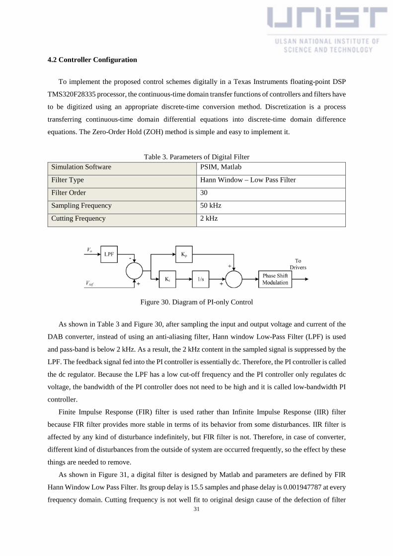
Table 3. Parameters of Digital Filter Simulation Software PSIM, Matlab
Filter Type Hann Window – Low Pass Filter
Filter Order 30
Sampling Frequency 50 kHz
Cutting Frequency 2 kHz
Figure 30. Diagram of PI-only Control
As shown in Table 3 and Figure 30, after sampling the input and output voltage and current of the
DAB converter, instead of using an anti-aliasing filter, Hann window Low-Pass Filter (LPF) is used
and pass-band is below 2 kHz. As a result, the 2 kHz content in the sampled signal is suppressed by the
LPF. The feedback signal fed into the PI controller is essentially dc. Therefore, the PI controller is called
the dc regulator. Because the LPF has a low cut-off frequency and the PI controller only regulates dc
voltage, the bandwidth of the PI controller does not need to be high and it is called low-bandwidth PI
controller.
Finite Impulse Response (FIR) filter is used rather than Infinite Impulse Response (IIR) filter
because FIR filter provides more stable in terms of its behavior from some disturbances. IIR filter is
affected by any kind of disturbance indefinitely, but FIR filter is not. Therefore, in case of converter,
different kind of disturbances from the outside of system are occurred frequently, so the effect by these
things are needed to remove.
As shown in Figure 31, a digital filter is designed by Matlab and parameters are defined by FIR
Hann Window Low Pass Filter. Its group delay is 15.5 samples and phase delay is 0.001947787 at every
frequency domain. Cutting frequency is not well fit to original design cause of the defection of filter 31

order. It is possible to fix this problem with increasing the filter order, but it is not appropriate for DSP
implementation cause of calculation burden. However we have to fulfill the minimum requirement of
statistical central limit theorem that the number of sample is at least 30.
Figure 31. Design Digital Filter with Matlab
Until now, conventional PI controller is implemented and from now, the proposed algorithm which
is an artificial intelligence gain-scheduling adaptive PI controller will be described as shown Table 4.
Table 4. Parameters of DBN Pre-training Learning Rate 0.1
Pre-training Epochs 500
Contrastive Divergence k 1
Fine-tuning Learning Rate 0.1
Fine-tuning Epochs 250
Hidden-Layer Sizes [ 3, 3, 3 ]
Number of Layers 3
Number of Inputs 4 ( Input and Output Voltage and Current)
Number of Outputs 3 ( Higher, Lower or Same as Reference Point )
32
Defining the variable of learning rate is a kind of hard problem and in most cases, learning rate starts
with 0.01 is appropriate and it is the most balanced point between rapid and stable. Moreover, the best
way to defining the learning rate is continuously decreasing from high learning rate to low learning rate.
It will make a rapid converging and a delicate manipulating. However, in this case, 0.1 is valuable in
terms of DSP which has a limited computing power for calculation. Computing power is limited and
calculation time is also limited because of real-time controller.
As more training epochs exist, as more accurate predicted probabilities produce. Pre-training is an
unsupervised learning procedure and fine-tuning is a supervised learning procedure. Therefore pre-
training is more epochs needed rather than fine-tuning. However there exists calculation and time limit
in this controller, so epochs are suggested like above values.
In ideal case, the number of hidden layer is defined as 6~7 layers or higher and size is like bell shape
– gradually increase and then decrease. Actually, most of users of DBN prefer to use lots of layers for
improving the result. However, DSP has a limited calculation time.
With these parameters, DBN predict the conditional probabilities of the state space which consists
of higher, lower or same as the reference point. Integrating the whole variables probabilities multiplied
by each status variables such as -1 (going down), 0 (maintain), 1 (going up) and then by using this
values it is possible to get the ultimate value of gain tuning value Ku. At last, multiplying with weight
of each gain value such as Wp, Wi, Wd, we can get the increase or decrease amount for each gain.
In this kind of method, there exists one problem which is possible to arise the stability problem. For
guaranteeing the stability problem, truncating the upper and the lower limit of each gain variable is a
possible solution for this system. Therefore middle value of each gain is fixed Kp and Ki and each case
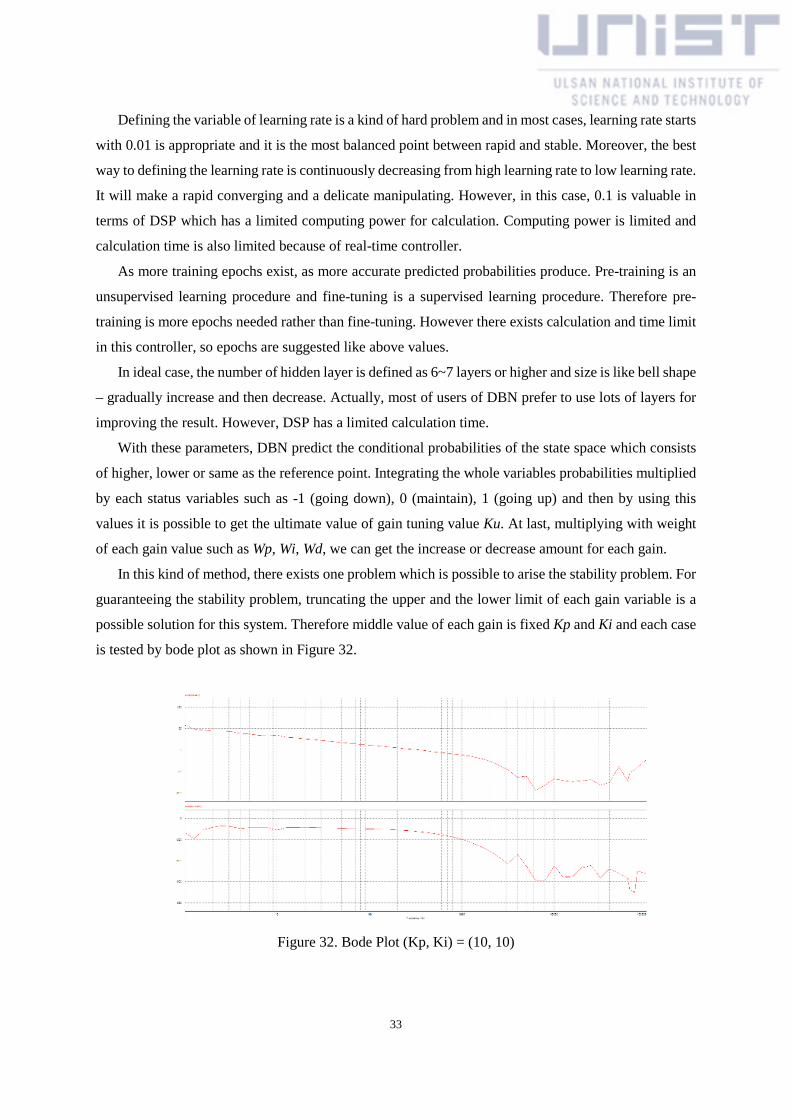
is tested by bode plot as shown in Figure 32.
Figure 32. Bode Plot (Kp, Ki) = (10, 10)
33

Figure 33. Proposed Algorithm Flow Chart
Figure 34. ADC Sampling Period, PWM Period and Computation Time Delay
As shown in Figure 33 and 34, the proposed algorithm needs more burden like calculating DBN
algorithm for updating PID gain variables. Each PWM period is only 20us around computation 3000
cycles of 150MHz DSP unit. Moreover, DBN algorithm is more complex than conventional one. 34

4.3 Simulation and Experimental Results
Figure 35. Conventional (Top) and Proposed (Bottom) Simulation Waveform
In the simulation shown in Figure 35, load conditions are varying, no load from the beginning, load
-8.7A at t=0.05 and load 8.7A at t=0.1, respectively. Furthermore, components attenuation such as
leakage degradation start at t=0.15. Every 0.02sec, proposed algorithm updates gain of PID controller.
As a result, step load response of the proposed algorithm is improved as 20us and the steady state error
decrease about 3V.
35
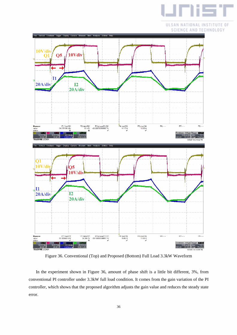
Figure 36. Conventional (Top) and Proposed (Bottom) Full Load 3.3kW Waveform
In the experiment shown in Figure 36, amount of phase shift is a little bit different, 3%, from
conventional PI controller under 3.3kW full load condition. It comes from the gain variation of the PI
controller, which shows that the proposed algorithm adjusts the gain value and reduces the steady state
error.
36

Figure 37. Conventional (Left) and Proposed (Right) Waveform of Starting Point
Figure 38. Conventional (Left) and Proposed (Right) Waveform of Load Variation from 8.7A to 4.3A
Figure 39. Conventional (Left) and Proposed (Right) Waveform of Load Variation from 4.3A to 8.7A
In the experiment shown in Figure 37, 38 and 39, dynamics of proposed algorithm is better than
conventional one in terms of variation of transient. When load is changed in order to confirm the
response transient of step load, proposed algorithm performs more stable than conventional one. In
addition, proposed algorithm remove low frequency oscillation at steady state.
37

Figure 40. Efficiency of Conventional (Left) and Proposed (Proposed) Full Load 3.3kW
Figure 41. Efficiency of Experimental Hardware
In the experiment shown in Figure 40 and 41, the trend of efficiency is the lowest in light load, the
highest in middle load and high in full load. The reason is that converter always consumes certain
amount of energy like switching loss, conduction loss, heat and sound and freewheeling current.
Moreover, as more RMS current increases, as more loss increases in high load area.
The drawback of proposed algorithm is efficiency. Most of this loss can be come from high
frequency oscillation as switching frequency. This high frequency oscillation makes reducing efficiency
and increasing heat dissipation.
75
80
85
90
95
100
0 500 1000 1500 2000 2500 3000 3500
%
W
Conventional Proposed
38

V. Discussion and Conclusion
The objective of this dissertation is to analyze three different aspects of DAB converters for SST
applications. DAB converters have some specific characteristics, which require analysis approaches,
modeling techniques, and control schemes.
Different SST topologies have their own advantages and disadvantages. Some have more
functionalities and complicated circuits, while some others lack reactive power control but have a
simpler circuit. The proposed topology uses the nonzero transformer leakage inductance to facilitate
voltage regulation and soft-switching. Four-quadrant switch cells and phase-shift modulation ensure
that energy can flow in both directions. This work presents a proof-of-concept study of applying dc-dc
DAB converters as SSTs.
Average models of DAB converters are necessary for the analysis and design of DAB converters.
Most previously theory have assumed that the dynamics of DAB converters can be approximated by a
reduced-order model. The reason for such approximation is the pure ac transformer current of DAB
converter, which is difficult to model using the conventional averaging technique. This dissertation
provides a first order continuous-time model for DAB converters by using the generalized state-space
averaging technique.
In the multi-stage configuration of SSTs, a dc-dc DAB converter is in between the rectifier stage
and the inverter stage. Since both the rectifier and the inverter process ac power. It is useful to enable
the DAB converter with such ability so that both average power and ripple power can be transferred in
a streamline.
This dissertation provides the new control method for dc-dc DAB converters to track the non-linear
time varying system affected by temperature, product variation, load disturbances and etc. Moreover,
experimental results show improvements in transient as well as steady state response of the proposed
controller over the conventional fixed PI controller.
5.1 Future Work
The dc-dc DAB converter makes possible to produce modular product and can be expanded easily
to a multiphase configuration. The input-series-output-parallel circuit configuration can block high
voltage on the primary side and share large current on the secondary side [67, 73].
The proposed average model of dc-dc DAB converters can be integrated with average models of
ac-dc rectifiers and dc-ac inverters to build an average model of an SST. Future work could use the SST
average model as a building block to model a large smart grid with a number of SSTs. A large system
of interconnected power electronic converters might have some complex or chaotic behaviors that are
39

worth analysis before actual hardware deployment. Moreover singular perturbation method needs to
apply the model for separating dc signal and ripple.
The next step in the analysis of a dc-dc DAB converter driving a dc-ac inverter could be adding
closed-loop control the inverter. When two regulated converters are in a cascaded connection, the well-
known negative impedance effect might be a challenge for controller design. The conventional rule-of-
thumb is to use a large dc bus capacitor, not only to absorb the harmonic current, but also to minimize
the de-stabilizing effect caused by the regulated load converter. An appropriate approach to model the
input impedance of a regulated inverter is necessary for such study.
Moreover, it is possible to change the switching frequency rather than fixed value. It means use not
only Pulse Width Modulation (PWM) method, but also Pulse Frequency Modulation (PFM) method in
order to improve the efficiency of converter at any range of load, especially, light load.
In addition, there exists several PWM methods such as Expanded Phase Shift (EPS) control, Dual
Phase Shift (DPS) control and Triple Phase Shift (TPS) control [128]. This dissertation focuses on
Single Phase Shift (SPS) control, but it is also possible to control each switches in order to reduce
reactive power and circulating current between the first bridge and the second bridge.
Future work could also focus on the general nonlinear control scheme to escape from specific
controller. The proposed controller focuses on the DAB converter, but the improved one can be possible
to control any kind of product which controller is needed and control non-linear time varying systems.
Moreover, in DBN, Gaussian process will be needed for the last layer in order to increase the accuracy
of prediction.
At last, the proposed algorithm code is located in appendix, but it needs to revise some structures
for real time running environment. The reason is that this code is originally appropriate to do some
experiments rather than real control.
40

References
[1] A. Huang, M. Crow, G. Heydt, J. Zheng, and S. Dale, “The Future Renewable Electric Energy Delivery and Management (FREEDM) System: The Energy Internet”, Proceedings of the IEEE, vol. 99, pp. 133–148, Jan. 2011.
[2] E. R. Ronan, S. D. Sudhoff, S. F. Glover, and D. L. Galloway, “A Power Electronic-based Distribution Transformer”, IEEE Power Engineering Review, vol. 22, pp. 61–61, Mar. 2002.
[3] H. Qin and J. W. Kimball, “AC-AC Dual Active Bridge Converter for Solid State Transformer”, in IEEE Energy Conversion Congress and Exposition (ECCE), 2009, pp. 3039–3044, 2009.
[4] M. Kang, P. N. Enjeti, and I. J. Pitel, “Analysis and Design of Electronic Transformers for Electric Power Distribution System”, IEEE Transactions on Power Electronics, vol. 14, pp. 1133–1141, Jun. 1999.
[5] M. H. Kheraluwala, R. W. Gascoigne, D. M. Divan, and E. D. Baumann, “Performance Characterization of a High-Power Dual Active Bridge DC-to-DC Converter”, IEEE Transactions on Industry Applications, vol. 28, no. 6, pp. 1294–1301, Nov./Dec. 1992.
[6] R. Lenke, F. Mura, and R. W. De Doncker, “Comparison of Non-Resonant and Super-Resonant Dual-Active ZVS-Operated High-Power DC-DC Converters”, Proc. of the 13th European Conference on Power Electronics and Applications (EPE 2009), Barcelona, Spain, 8–10 Sep. 2009.
[7] J. Biela, U. Badstübner, and J. W. Kolar, “Design of a 5 kW, 1 U, 10 kW/ltr. Resonant DC-DC Converter for Telecom Applications”, Proc. of the 29th International Telecommunications Energy Conference (INTELEC 2007), Rome, Italy, 30 Sept.–4 Oct. 2007, pp. 824–831.
[8] F. Peng, H. Li, G.-J. Su, and J. Lawler, “A New ZVS Bidirectional DC-DC Converter for Fuel Cell and Battery Application”, IEEE Transactions on Power Electronics, vol. 19, pp. 54–65, Jan. 2004.
[9] D. Xu, C. Zhao, and H. Fan, “A PWM plus Phase-Shift Control Bidirectional DC-DC Converter”, IEEE Transactions on Power Electronics, vol. 19, pp. 666–675, Mar. 2004.
[10] H. Xiao and S. Xie, “A ZVS Bidirectional DC-DC Converter with Phase-Shift plus PWM Control Scheme”, IEEE Transactions on Power Electronics, vol. 23, pp. 813–823, Mar. 2008.
[11] H. Bai and C. Mi, “Eliminate Reactive Power and Increase System Efficiency of Isolated Bidirectional Dual-Active-Bridge DC-DC Converters using Novel Dual-Phase-Shift Control”, IEEE Transactions on Power Electronics, vol. 23, pp. 2905–2914, Nov. 2008.
[12] Z. Haihua and A. M. Khambadkone, “Hybrid Modulation for Dual-Active-Bridge Bidirectional Converter with Extended Power Range for Ultra-Capacitor Application”, IEEE Transactions on Industry Application, vol. 45, pp. 1434–1442, Apr. 2009.
[13] G. Oggier, G. Garcianda, and A. Oliva, “Modulation Strategy to Operate the Dual Active Bridge DC-DC Converter under Soft Switching in the Whole Operating Range”, IEEE Transactions on Power Electronics, vol. 26, pp. 1228–1236, Apr. 2011.
41

[14] J. Kim, I. Jeong, and K. Nam, “Asymmetric Duty Control of the Dual-Active-Bridge DC/DC Converter for Single-Phase Distributed Generators”, IEEE Energy Conversion Congress and Exposition (ECCE), pp. 75–82, Sept. 2009.
[15] H. Plesko, J. Biela, and J. Kolar, “Novel Modulation Concepts for a Drive-Integrated Auxiliary DC-DC Converter for Hybrid Vehicles”, IEEE Applied Power Electronics Conference and Exposition (APEC), pp. 164–170, Feb. 2009.
[16] A. Jain and R. Ayyanar, “PWM Control of Dual Active Bridge: Comprehensive Analysis and Experimental Verification”, 34th Annual Conference of IEEE Industrial Electronics (IECON), pp. 909–915, Nov. 2008.
[17] A. Jain and R. Ayyanar, “PWM Control of Dual Active Bridge: Comprehensive Analysis and Experimental Verification”, IEEE Transactions on Power Electronics, vol. 26, pp. 1215–1227, Apr. 2011.
[18] J. Kim, H.-S. Song, and K. Nam, “Asymmetric Duty Control of a Dual-Half-Bridge DC/DC Converter for Single-Phase Distributed Generators”, IEEE Transactions on Power Electronics, vol. 26, pp. 973–982, Mar. 2011.
[19] Y. Wang, S. W. H. de Haan, and J. A. Ferreira, “Optimal Operating Ranges of Three Modulation Methods in Dual Active Bridge Converters”, IEEE 6th International Power Electronics and Motion Control Conference (IPEMC), pp. 1397–1401, 2009.
[20] G. G. Oggier, G. O. Garcia, and A. R. Oliva, “Switching Control Strategy to Minimize Dual Active Bridge Converter Losses”, IEEE Transactions on Power Electronics, vol. 24, pp. 1826–1838, Jul. 2009.
[21] B. Hua, C. C. Mi, and S. Gargies, “The Short-Time-Scale Transient Processes in High-Voltage and High-Power Isolated Bidirectional DC-DC Converters”, IEEE Transactions on Power Electronics, vol. 23, pp. 2648–2656, Jun. 2008.
[22] Y. Xie, J. Sun, and J. S. Freudenberg, “Power Flow Characterization of a Bidirectional Galvanically Isolated High-Power DC/DC Converter over a Wide Operating Range”, IEEE Transactions on Power Electronics, vol. 25, pp. 54–66, Jan. 2010.
[23] F. Krismer and J. Kolar, “Accurate Power Loss Model Derivation of a High-Current Dual Active Bridge Converter for an Automotive Application”, IEEE Transactions on Industrial Electronics, vol. 57, pp. 881–891, Mar. 2010.
[24] H. Qin and J. Kimball, “A Comparative Efficiency Study of Silicon-based Solid State Transformers”, IEEE Energy Conversion Congress and Exposition (ECCE), pp. 1458–1463, Sept. 2010.
[25] F. Krismer, S. Round, and J. Kolar, “Performance Optimization of a High Current Dual Active Bridge with a Wide Operating Voltage Range”, IEEE Power Electronics Specialists Conference (PESC), pp. 1–7, Jun. 2006.
42

[26] J. Biela, U. Badstubner, and J. Kolar, “Design of a 5kW, 1U, 10kW/ltr. Resonant DC-DC Converter for Telecom Applications”, IEEE International Telecommunications Energy Conference (INTELEC), pp. 824–831, Oct. 2007.
[27] D. Aggeler, J. Biela, and J. Kolar, “A Compact, High Voltage 25 kW, 50 kHz DC-DC Converter based on SiC JFETs”, IEEE Applied Power Electronics Conference and Exposition (APEC), pp. 801–807, Feb. 2008.
[28] C. Mi, H. Bai, C. Wang, and S. Gargies, “Operation, Design and Control of Dual H-Bridge-based Isolated Bidirectional DC-DC Converter”, IET Power Electronics, vol. 1, pp. 507–517, Dec. 2008.
[29] Y. Wang, S. de Haan, and J. Ferreira, “High Power Density Design of High-Current DC-DC Converter with High Transient Power”, IEEE Energy Conversion Congress and Exposition (ECCE), pp. 3001–3008, Sept. 2010.
[30] G. Ortiz, J. Biela, D. Bortis, and J. Kolar, “1 Megawatt, 20 kHz, Isolated, Bidirectional 12kV to 1.2kV DC-DC Converter for Renewable Energy Applications”, International Power Electronics Conference (IPEC), pp. 3212–3219, Jun. 2010.
[31] F. Krismer and J. Kolar, “Efficiency-Optimized High Current Dual Active Bridge Converter for Automotive Applications”, IEEE Transactions on Industrial Electronics, vol. PP, p. 1, Nov 2011.
[32] R. Morrison and M. Egan, “A New Power-Factor-Corrected Single-Transformer UPS Design”, IEEE Transactions on Industry Application, vol. 36, pp. 171–179, Jan./Feb. 2000.
[33] F. Krismer, J. Biela, and J. Kolar, “A Comparative Evaluation of Isolated Bidirectional DC/DC Converters with Wide Input and Output Voltage Range”, IEEE Industry Applications Society (IAS) Annual Meeting, vol. 1, pp. 599–606, Oct. 2005.
[34] H. Tao, A. Kotsopoulos, J. Duarte, and M. Hendrix, “Transformer-Coupled Multiport ZaVS Bidirectional DC-DC Converter with Wide Input Range”, IEEE Transactions on Power Electronics, vol. 23, pp. 771–781, Mar. 2008.
[35] J. Duarte, M. Hendrix, and M. Simoes, “Three-Port Bidirectional Converter for Hybrid Fuel Cell Systems”, IEEE Transactions on Power Electronics, vol. 22, pp. 480–487, Mar. 2007.
[36] J. Walter and R. De Doncker, “High-Power Galvanically Isolated DC-DC Converter Topology for Future Automobiles”, IEEE Power Electronics Specialist Conference (PESC), vol. 1, pp. 27–32, Jun. 2003.
[37] S. Han and D. Divan, “Bi-Directional DC/DC Converters for Plug-in Hybrid Electric Vehicle (PHEV) Applications”, IEEE Applied Power Electronics Conference and Exposition (APEC), pp. 784–789, Feb. 2008.
[38] J. Ming Hu, Y. Rui Chen, and Z. Juan Yang, “Study and Simulation of One Bi-Directional DC/DC Converter in Hybrid Electric Vehicle”, International Conference on Power Electronics Systems and Applications (PESA), pp. 1–4, May 2009.
[39] Y.-J. Lee and A. Emadi, “Integrated Bi-Directional AC/DC and DC/DC Converter for Plug-in Hybrid Electric Vehicle Conversion”, IEEE Vehicle Power and Propulsion Conference (VPPC), pp. 215–222, Sept. 2007.
43
[40] D. Erb, O. Onar, and A. Khaligh, “An Integrated Bi-Directional Power Electronic Converter with Multi-Level AC-DC/DC-AC Converter and Non-Inverted Buck-Boost Converter for PHEVs with Minimal Grid Level Disruptions”, IEEE Vehicle Power and Propulsion Conference (VPPC), pp. 1–6, Sept. 2010.
[41] Y. Gurkaynak, Z. Li, and A. Khaligh, “A Novel Grid-Tied, Solar Powered Residential Home with Plug-in Hybrid Electric Vehicle (PHEV) Loads”, IEEE Vehicle Power and Propulsion Conference (VPPC), pp. 813–816, Sept. 2009.
[42] S. Inoue and H. Akagi, “A Bidirectional Isolated DC-DC Converter as a Core Circuit of the Next-Generation Medium-Voltage Power Conversion System”, IEEE Transactions on Power Electronics, vol. 22, pp. 535–542, Feb. 2007.
[43] S. Inoue and H. Akagi, “A Bidirectional DC-DC Converter for an Energy Storage System with Galvanic Isolation”, IEEE Transactions on Power Electronics, vol. 22, pp. 2299–2306, Nov. 2007.
[44] S. Inoue and H. Akagi, “A Bi-Directional DC/DC Converter for an Energy Storage System”, Twenty Second Annual IEEE Applied Power Electronics Conference (APEC), pp. 761–767, Mar. 2007.
[45] N. Tan, N. Tan, S. Inoue, S. Inoue, A. Kobayashi, and H. Akagi, “Voltage Balancing of a 320-V, 12-F Electric Double-Layer Capacitor Bank Combined with a 10-kW Bidirectional Isolated DC-DC Converter”, IEEE Transactions on Power Electronics, vol. 23, pp. 2755–2765, Nov. 2008.
[46] H. Tao, A. Kotsopoulos, J. Duarte, and M. Hendrix, “Triple-Half-Bridge Bidirectional Converter Controlled by Phase Shift and PWM”, IEEE Applied Power Electronics Conference and Exposition (APEC), pp. 7–13, Mar. 2006.
[47] Z. Chuanhong, S. D. Round, and J. W. Kolar, “An Isolated Three-Port Bidirectional DC-DC Converter with Decoupled Power Flow Management”, IEEE Transactions on Power Electronics, vol. 23, pp. 2443–2453, Sept. 2008.
[48] H. Krishnaswami and N. Mohan, “Three-Port Series-Resonant DC-DC Converter to Interface Renewable Energy Sources with Bidirectional Load and Energy Storage Ports”, IEEE Transactions on Power Electronics, vol. 24, pp. 2289–2297, Oct. 2009.
[49] F. Golnaraghi and B. C. Kuo, Automatic Control Systems 9th Ed., Wiley, 2009.
[50] S. Middlebrook, S. Cuk, “A General Unified Approach to Modeling Switching Converter Power Stages”, Proc. of IEEE Power Electronics Specialists Conference, 1976, pp. 18–34, 1976.
[51] S. Middlebrook, S. Cuk, “A General Unified Approach to Modeling Switching DC-to-DC Converters in Discontinuous Conduction Mode”, Proc. of IEEE Power Electronics Specialists Conference, pp. 36–57, 1977.
[52] R. Middlebrook, “Small-Signal Modeling of Pulse-Width Modulated Switched-Mode Power Converters”, Proceedings of the IEEE, vol. 76, pp. 343–354, Apr. 1988.
[53] D. Maksimovic, A. Stankovic, V. Thottuvelil, and G. Verghese, “Modeling and Simulation of Power Electronic Converters”, Proceedings of the IEEE, vol. 89, pp. 898–912, Jun. 2001.
44

[54] B. Lehman and R. Bass, “Switching Frequency Dependent Averaged Models for PWM DC-DC Converters”, IEEE Transactions on Power Electronics, vol. 11, pp. 89–98, Jan 1996.
[55] S. R. Sanders, Noworolski, J. M., X. Z. Liu, and G. C. Verghese, “Generalized Averaging Method for Power Conversion Circuits”, IEEE Transactions on Power Electronics, vol. 6, pp. 251–259, Feb. 1991.
[56] J. Sun and H. Grotstollen, “Symbolic Analysis Methods for Averaged Modeling of Switching Power Converters”, IEEE Transactions on Power Electronics, vol. 12, pp. 537–546, May 1997.
[57] V. A. Caliskan, O. C. Verghese, and A. M. Stankovic, “Multi-Frequency Averaging of DC/DC Converters”, IEEE Transactions on Power Electronics, vol. 14, pp. 124–133, Jan. 1999.
[58] Z. Mihajlovic, B. Lehman, and C. Sun, “Output Ripple Analysis of Switching DC-DC Converters”, IEEE Transactions on Circuits and Systems I: Regular Papers, vol. 51, pp. 1596–1611, Aug. 2004.
[59] C.-C. Hou and P.-T. Cheng, “Experimental Verification of the Active Front-End Converters Dynamic Model and Control Designs”, IEEE Transactions on Power Electronics, vol. 26, pp. 1112–1118, Apr. 2011.
[60] P. Krein, J. Bentsman, R. Bass, and B. Lesieutre, “On the Use of Averaging for the Analysis of Power Electronic Systems”, IEEE Transactions on Power Electronics, vol. 5, pp. 182–190, Feb. 1990.
[61] P. Krein and R. Bass, “A New Approach to Fast Simulation of Periodically Switching Power Converters”, IEEE Industry Applications Society (IAS) Annual Meeting, 1990, pp. 1185–1189, Oct 1990.
[62] D. Shortt and F. Lee, “Improved Switching Converter Model using Discrete and Averaging Techniques”, IEEE Transactions on Aerospace and Electronic Systems, vol. 19, pp. 190–202, Mar. 1983.
[63] D. Shortt and F. Lee, “Extensions of the Discrete-Average Models for Converter Power Stages”, IEEE Transactions on Aerospace and Electronic Systems, vol. 20, pp. 279–289, May 1984.
[64] G. C. Verghese, M. E. Elbuluk, and J. G. Kassakian, “A General Approach to Sampled-Data Modeling for Power Electronic Circuits”, IEEE Transactions on Power Electronics, vol. 1, pp. 76–89, Apr. 1986.
[65] M. Elbuluk, G. Verghese, and J. Kassakian, “Sampled-Data Modeling and Digital Control of Resonant Converters”, IEEE Transactions on Power Electronics, vol. 3, pp. 344–354, Jul. 1988.
[66] S. Zheng and D. Czarkowski, “Modeling and Digital Control of a Phase-Controlled Series-Parallel Resonant Converter”, IEEE Transactions on Industrial Electronics, vol. 54, pp. 707–715, Apr. 2007.
[67] H. K. Krishnamurthy and R. Ayyanar, “Building Block Converter Module for Universal (AC-DC, DC-AC, DC-DC) fully Modular Power Conversion Architecture”, IEEE Power Electronics Specialists Conference (PECS), pp. 483–489, 2007.
45

[68] B. Hua, C. C. Mi, and S. Gargies, “The Short-Time-Scale Transient Processes in High-Voltage and High-Power Isolated Bidirectional DC-DC Converters”, IEEE Transactions on Power Electronics, vol. 23, pp. 2648–2656, Jun. 2008.
[69] H. Bai, Z. Nie, and C. C. Mi, “Experimental Comparison of Traditional Phase-Shift, Dual-Phase-Shift, and Model-based Control of Isolated Bidirectional DC-DC Converters”, IEEE Transactions on Power Electronics, vol. 25, pp. 1444–1449, Jun. 2010.
[70] F. Krismer and J. W. Kolar, “Accurate Small-Signal Model for the Digital Control of an Automotive Bidirectional Dual Active Bridge”, IEEE Transactions on Power Electronics, vol. 24, pp. 2756–2768, Dec. 2009.
[71] C. Zhao, S. D. Round, and J. W. Kolar, “Full-Order Averaging Modelling of Zero-Voltage-Switching Phase-Shift Bidirectional DC-DC Converters”, IET Power Electronics, vol. 3, pp. 400–410, Mar. 2010.
[72] P. Kokotovic, H. K. Khalil, and J. O’Reilly, Singular Perturbation Methods in Control Analysis and Design. London, U.K.: Academic, 1999.
[73] J. W. Kimball, J. T. Mossoba, and P. T. Krein, “A Stabilizing, High-Performance Controller for Input Series-Output Parallel Converters”, IEEE Transactions on Power Electronics, vol. 23, pp. 1416–1427, Mar. 2008.
[74] J. Reeve and M. Sultan, “Robust Adaptive Control of HVDC Systems”, IEEE Transactions on Power Delivery, vol. 9, pp. 1487–1493, Jul. 1994.
[75] M. AI-Numay and D. Taylor, “A Piecewise Linear Method for Digital Control of PWM Systems”, IEEE Power Electronics Specialists Conference (PESC), vol. 1, pp. 803–809, Jun 1996.
[76] A. Prodic and D. Maksimovic, “Design of a Digital PID Regulator based on Look-up Tables for Control of High-Frequency DC-DC Converters”, IEEE Workshop on Computers in Power Electronics, pp. 18–22, Jun. 2002.
[77] A. Forsyth, I. Ellis, and M. Moller, “Adaptive Control of a High-Frequency DC-DC Converter by Parameter Scheduling”, IEE Proceedings - Electric Power Applications, vol. 146, pp. 447–454, Jul. 1999.
[78] K. J. Astrom and B. Wittenmark, Adaptive Control: Second Edition. Dover Publications, 2008.
[79] M. Hernandez-Gomez, R. Ortega, F. Lamnabhi-Lagarrigue, and G. Escobar, “Adaptive PI Stabilization of Switched Power Converters”, IEEE Transactions on Control Systems Technology, vol. 18, pp. 688–698, May 2010.
[80] L. Yacoubi, K. Al-Haddad, L.-A. Dessaint, and F. Fnaiech, “Linear and Nonlinear Control Techniques for a Three-Phase Three-Level NPC Boost Rectifier”, IEEE Transactions on Industrial Electronics, vol. 53, pp. 1908–1918, Dec. 2006.
[81] S. Vazquez, J. Sanchez, J. Carrasco, J. Leon, and E. Galvan, “A Model-based Direct Power Control for Three-Phase Power Converters”, IEEE Transactions on Industrial Electronics, vol. 55, pp. 1647–1657, Apr. 2008.
46

[82] Z. Jiang, L. Gao, and R. Dougal, “Adaptive Control Strategy for Active Power Sharing in Hybrid Fuel Cell/Battery Power Sources”, IEEE Transactions on Energy Conversion, vol. 22, pp. 507–515, Jun. 2007.
[83] S. Sanders and G. Verghese, “Lyapunov-based Control for Switched Power Converters”, IEEE Transactions on Power Electronics, vol. 7, pp. 17–24, Jan. 1992.
[84] R. Ortega, A. Loria, P. Nicklasson, and H. Sira-Ramirez, Passivity-Based Control of Euler-Lagrange Systems. Springer, 1998.
[85] S. Banerjee and G. Verghese, Nonlinear Phenomena in Power Electronics: Bifurcations, Chaos, Control, and Applications. Wiley-IEEE Press, 2001.
[86] D. Jeltsema and J. Scherpen, “A Power-based Perspective in Modeling and Control of Switched Power Converters [Past and Present]”, IEEE Industrial Electronics Magazine, vol. 1, pp. 7–54, May 2007.
[87] H. Zhou, A. Khambadkone, and X. Kong, “Passivity-based Control for an Interleaved Current-Fed Full-Bridge Converter with a Wide Operating Range using the Brayton-moser Form”, IEEE Transactions on Power Electronics, vol. 24, pp. 2047–2056, Sept. 2009.
[88] L. Harnefors, M. Bongiorno, and S. Lundberg, “Input-Admittance Calculation and Shaping for Controlled Voltage-Source Converters”, IEEE Transactions on Industrial Electronics, vol. 54, pp. 3323–3334, Dec. 2007.
[89] L. Harnefors, L. Zhang, and M. Bongiorno, “Frequency-Domain Passivity-based Current Controller Design”, IET Power Electronics, vol. 1, pp. 455–465, Dec. 2008.
[90] K. Young, V. Utkin, and U. Ozguner, “A Control Engineer’s Guide to Sliding Mode Control”, IEEE Transactions on Control Systems Technology, vol. 7, pp. 328–342, May 1999.
[91] S.-C. Tan, Y. Lai, C. Tse, and L. Martinez-Salamero, “Special Family of PWM-based Sliding-Mode Voltage Controllers for Basic DC-DC Converters in Discontinuous Conduction Mode”, IET Electric Power Applications, vol. 1, pp. 64–74, Jan. 2007.
[92] S.-C. Tan, Y. Lai, C. Tse, and M. Cheung, “Adaptive Feedforward and Feedback Control Schemes for Sliding Mode Controlled Power Converters”, IEEE Transactions on Power Electronics, vol. 21, pp. 182–192, Jan. 2006.
[93] S. Pinto and J. Silva, “Sliding Mode Direct Control of Matrix Converters”, IET Electric Power Applications, vol. 1, pp. 439–448, May 2007.
[94] A. Susperregui, G. Tapia, I. Zubia, and J. Ostolaza, “Sliding-Mode Control of Doubly-Fed Generator for Optimum Power Curve Tracking”, Electronics Letters, vol. 46, pp. 126–127, Nov. 2010.
[95] Z. Chen, W. Gao, J. Hu, and X. Ye, “Closed-loop Analysis and Cascade Control of a Non-Minimum Phase Boost Converter”, IEEE Transactions on Power Electronics, vol. 26, pp. 1237–1252, Apr. 2011.
47
[96] C.-F. Hsu, I.-F. Chung, C.-M. Lin, and C.-Y. Hsu, “Self-Regulating Fuzzy Control for Forward DC-DC Converters using an 8-bit Microcontroller”, IET Power Electronics, vol. 2, pp. 1–12, Jan. 2009.
[97] M. Zandi, A. Payman, J.-P. Martin, S. Pierfederici, B. Davat, and F. Meibody-Tabar, “Energy Management of a Fuel Cell/Supercapacitor/Battery Power Source for Electric Vehicular Applications”, IEEE Transactions on Vehicular Technology, vol. 60, pp. 433–443, Feb. 2011.
[98] C. Cecati, F. Ciancetta, and P. Siano, “A Multilevel Inverter for Photovoltaic Systems with Fuzzy Logic Control”, IEEE Transactions on Industrial Electronics, vol. 57, pp. 4115–4125, Dec. 2010.
[99] A. Bouafia, F. Krim, and J.-P. Gaubert, “Fuzzy-Logic-based Switching State Selection for Direct Power Control of Three-Phase PWM Rectifier”, IEEE Trans-actions on Industrial Electronics, vol. 56, pp. 1984–1992, Jun. 2009.
[100] D. Cardozo, J. Balda, D. Trowler, and H. Mantooth, “Novel Nonlinear Control of Dual Active Bridge using Simplified Converter Model”, IEEE Twenty-Fifth Annual Applied Power Electronics Conference and Exposition (APEC), pp. 321–327, Feb. 2010.
[101] A. Alonso, J. Sebastian, D. Lamar, M. Hernando, and A. Vazquez, “An Overall Study of a Dual Active Bridge for Bidirectional DC/DC Conversion”, IEEE Energy Conversion Congress and Exposition (ECCE), pp. 1129–1135, Sept. 2010.
[102] D. Segaran, B. McGrath, and D. Holmes, “Adaptive Dynamic Control of a Bidirectional DC-DC Converter”, IEEE Energy Conversion Congress and Exposition (ECCE), pp. 1442–1449, Sept. 2010.
[103] G. Demetriades and H.-P. Nee, “Dynamic Modeling of the Dual-Active Bridge Topology for High-Power Applications”, IEEE Power Electronics Specialists Conference (PESC), pp. 457–464, Jun. 2008.
[104] J. Shi, W. Gou, H. Yuan, T. Zhao, and A. Huang, “Research on Voltage and Power Balance Control for Cascaded Modular Solid-State Transformer”, IEEE Transactions on Power Electronics, vol. 26, pp. 1154–1166, Apr. 2011.
[105] H. Akagi and R. Kitada, “Control and Design of a Modular Multilevel Cascade btb System using Bidirectional Isolated DC/DC Converters”, IEEE Transactions on Power Electronics, vol. 26, pp. 2457–2464, Sept. 2011.
[106] F. Krismer, “Modeling and Optimization of Bidirectional Dual Active Bridge DC-DC Converter Topologies”, ETH Doctoral Thesis, pp. 50-53, 2010.
[107] Sreejith Nair, “Control Machines with Your Machine”, http://fsmsh.com/1267, Free Software Magazine, 2007.
[108] Yoshua Bengio, “Learning Deep Architectures for AI”, Foundations and Trends in Machine Learning, vol. 2, pp. 1-127, 2009.
[109] Roger Grosse, “Deep Learning from the Bottom Up”, Matacademy, http://metacademy.org/roadmaps/rgrosse/deep_learning , 2014.
48

[110] Ziegler, J.G. and Nochols, N. B., “Optimum Settings for Automatic Controllers”, Transactions of the ASME, vol. 64, pp. 759-768, 1942.
[111] Ranzato, M., Boureau, Y.-L., & LeCun, Y., “Sparse Feature Learning for Deep Belief Networks”, Advances in Neural Information Processing Systems (NIPS 2007), MIT Press, 2008.
[112] Hinton, G. E., Osindero, S., & Teh, Y., “A Fast Learning Algorithm for Deep Belief Nets”, Neural Computation, vol. 18, pp. 1527–1555, 2006.
[113] Bengio, Y., Lamblin, P., Popovici, D., & Larochelle, H., “Greedy Layer-Wise Training of Deep networks”, Scholkopf, B., Platt, J., & Hoffman, T. (Eds.), Advances in Neural Information Processing Systems, vol. 19, pp. 153–160, MIT Press, 2007.
[114] LeCun, Y., Chopra, S., Hadsell, R., Ranzato, M.-A., & Huang, F.-J., “A Tutorial on Energy-based Learning”, Bakir, G., Hofman, T., Scholkopf, B., Smola, A., & Taskar, B. (Eds.), Predicting Structured Data. MIT Press, 2006.
[115] Freund, Y., & Haussler, D., “Unsupervised Learning of Distributions on Binary Vectors using Two Layer Networks”, Tech. rep. UCSC-CRL-94-25, University of California, Santa Cruz, 1994.
[116] Le Roux, N., & Bengio, Y.,” Representational Power of Restricted Boltzmann Machines and Deep Belief Networks”, Neural Computation, 2008.
[117] Geman, S., & Geman, D., “Stochastic Relaxation, Gibbs Distributions, and the Bayesian Restoration of Images”, IEEE Transactions on Pattern Analysis and Machine Intelligence, vol. 6, 1984.
[118] Andrieu, C., de Freitas, N., Doucet, A., & Jordan, M., “An Introduction to MCMC for Machine Learning”, Machine Learning, vol. 50, pp. 5–43, 2003.
[119] Bengio, Y., & Delalleau, O., “Justifying and Generalizing Contrastive Divergence”, Tech. rep. 1311, Dept. IRO, Universite´ de Montre´al, 2007.
[120] Carreira-Perpinan, M., & Hinton, G., “On Contrastive Divergence Learning”, Proceedings of the Tenth International Workshop on Artificial Intelligence and Statistics, Jan 6-8, 2005, Savannah Hotel, Barbados, 2005.
[121] Hinton, G., “Training Products of Experts by Minimizing Contrastive Divergence”, Neural Computation, vol. 14, pp. 1771–1800, 2002.
[122] Larochelle, H., Erhan, D., Courville, A., Bergstra, J., & Bengio, Y., “An Empirical Evaluation of Deep Architectures on Problems with Many Factors of Variation”, Twenty-fourth International Conference on Machine Learning (ICML’2007), 2007.
[123] “Protection Application – An Overview Introduction”, ABB Group, 2014.
[124] “Newest and Most Efficient Smart Solid-State Transformers”, Electrical Installation & Energy Efficiency Community, 2014
[125] M. Carreira-Perpinan and G.E. Hinton, “On Contrastive Divergence Learning”, Tenth International Workshop on Artificial Intelligence and Statistics, 2005.
49

[126] C. Mi, H. Bai, C. Wang, S. Gargies, “Operation, Design and Control of Dual H-bridge-based Isolated Bidirectional DC-DC Converter”, IET Power Electronics, vol. 1, no. 4, pp. 507-517, 2008.
[127] Alonzo Kelly, “A 3D State Space Formulation of a Navigation Kalman Filter for Autonomous Vehicles”, CMU-RI-TR-94-19-REV 2.0, 2006.
[128] Biao Zhao, Qiang Song, Wenhua Liu and Yandong Sun, “Overview of Dual-Active-Bridge Isolated Bidirectional DC-DC Converter for High-Frequency-Link Power-Conversion System”, IEEE Transactions on Power Electronics, vol. 29, no. 8, pp. 4091-4106, 2014.
[129] Hinton G. E. and Salakhutolinov R. R., “Reducing the Dimensionality of Data with Neural Networks”, Science, vol. 313, no. 5786, pp. 504-507, 2006.
50

Appendix
/*======================================================================= File name : main.c - DAB Purpose : Embedded Software for Controlling Power Converter Object : Bidirectional DC-DC Dual Active Bridge Converter Target : TMS320F28335 PGFA Rev. A Author : Kim Sul Gi ([email protected]) Copyright (c) 2014 Kim Sul Gi =======================================================================*/ /*======================================================================= History : 2011-02-21 Version 1.00 Original Code From KERI 2013-12-12 Version 1.10 Overhaul Re-factoring Kim Sul Gi 2014-02-13 Version 1.20 Minor Update Kim Sul Gi 2014-02-25 Version 2.00 Implement DBN Algorithm Kim Sul Gi 2014-03-07 Version 2.10 Memory Problem Fix Kim Sul Gi 2014-03-15 Version 2.20 FIR Filter Implementation Kim Sul Gi 2014-04-01 Version 2.30 Minor Program Optimization Kim Sul Gi 2014-04-08 Version 2.40 Filter Optimization Kim Sul Gi 2014-05-20 Version 2.50 Training Problem Fix Kim Sul Gi 2014-06-29 Version 2.60 Minor Program Optimization Kim Sul Gi =======================================================================*/ #include "DSP28x_Project.h" /* Device Header file and Examples Include File */ #include "DBN.h" // Deep Belief Network Header #include <Stdlib.h> #include <String.h> #include <math.h> /********************************* * Define Control Variables *********************************/ //#define SYSCLK 150000 // 150kHz TMS320F28335 //#define ST_BUFFSIZE 37500 // PHD-ST_PwmPeriod // Calibration from ADC to Real #define CCAL_1 456 // Calibration for Voltage 1 : 32-2.5, 2nd Old Value 45.6 / New Value 38.4 #define ICCAL_1 200 // Calibration for Current 1 : 200A, 3V #define CCAL_2 456 // Calibration for Voltage 2 : 380-2.5 #define ICCAL_2 25 // Calibration for Current 2 : 25A, 3V // For Filter Values
51

#define TC_FILTER_FREQUENCY_P 0.001 // Filter Frequency Primary - 1kHz, Max = 12.5MHz ADC #define TC_FILTER_FREQUENCY_S 0.00005 // Filter Frequency Secondary - 20kHz, Max = 12.5MHz ADC #define TSAMP 0.000013333 // Sampling Time - Following Switching Frequency - 75kHz, Max = 12.5MHz // PWM Period 12 500 000 - 1sec #define PWMPERIOD 1500 // Define Switching Period Length = {Tpwm / (Tsysclkout*CLKDIV*HSPCLKDIV)}/2 - 75kHz #define DUTY_CYCLE_1 0.5 // Duty Cycle (%) #define DUTY_CYCLE_2 0.5 // Duty Cycle (%) // Phase Shift #define ST_PHASE_DELAY_PERIOD 1000 // Phase delay period #define ST_PHASE_DELAY_MAX_PLUS 480 // Phase delay +MAX = 0.48 #define ST_PHASE_DELAY_MAX_MINUS 50 // Phase delay -MAX = 0.05 #define ST_PHASE_DELAY_MIN 1 // Phase delay MIN = 0.001 #define ST_PHASE_RATE 0.0125 // Phase delay rate for soft start - 0.005, 0.0125, 0.1 // Power Limited for Protection #define POWER_LIMIT 480 // Power Limit: P = V * I // Target Voltage and Current #define VREF_1 380 // Vout Reference #define VREF_2 380 // Vin Reference #define IREF_1 1 // Iout Reference #define IREF_2 1 // Iin Reference // PI Gain Values for Voltage and Current #define V_PG 0.5 // Voltage: Initialize P Weight : Pgain 5 #define V_IG 0.03 // Voltage: Initialize I Weight : Igain change to this from 0.03 #define V_DG 0 // Voltage: Initialize D Weight : Dgain #define V_IGAIN_LIMIT 480 // Voltage: I gain limit - 480 : Original #define V_DGAIN_LIMIT 10 // Voltage: D gain limit #define I_PG 0.009 // Current: Initialize Weight : P gain #define I_IG 0.001 // Current: Initialize Weight : I gain #define I_DG 0 // Current: Initialize Weight : D gain #define I_IGAIN_LIMIT 0.001 // Current: I gain limit - 0.001 : Original #define I_DGAIN_LIMIT 0 // Current: D gain limit #define I_PIGAIN_LIMIT 0.2 // Current: PI gain limit - 0.2 : Original // Refer External Value of RAM Program extern Uint16 RamfuncsLoadStart; extern Uint16 RamfuncsLoadEnd; extern Uint16 RamfuncsRunStart; /********************************************** * DBN Section **********************************************/
52

unsigned int time1 = 0; unsigned int time2 = 0; unsigned int time3 = 0; // For DBN Calculation int test[4] = {0, 0, 0, 0}; double result[3] = {0, 0, 0}; // Find Max Variable double max = 0; int max_flag = 0; // initialize dbn DBN *dbn; Uint16 dbn_flag = 1; // Init DBN Uint16 dbn_init_flag = 0; // 0:first time, 1:others // Generated by MATLAB(R) 8.1 and the Signal Processing Toolbox 6.19. // Generated on: 16-Apr-2014 22:32:53 // Coefficient Format: Decimal // Discrete-Time FIR Filter (real) // ------------------------------- // Filter Structure : Direct-Form FIR // Filter Length : 31 // Stable : Yes // Linear Phase : Yes (Type 1) // Coefficient for FIR Low Pass Filter : Cut-off - 2khz double h[31] = {0.0049101175751824471, 0.0055277554581381842, 0.0073527381677400781, 0.010305690094256597, 0.014257856059066931, 0.019036726240512874, 0.024433577992440263, 0.030212604589694644, 0.036121231339690009, 0.04190116740588555, 0.047299709384781528, 0.052080801582373243, 0.056035368538249836, 0.058990467183333478, 0.060816857696723348, 0.061434661383862249, 0.060816857696723348, 0.058990467183333478, 0.056035368538249836, 0.052080801582373243, 0.047299709384781528, 0.04190116740588555, 0.036121231339690009, 0.030212604589694644, 0.024433577992440263, 0.019036726240512874, 0.014257856059066931, 0.010305690094256597, 0.0073527381677400781, 0.0055277554581381842, 0.0049101175751824471}; // Initialize Sensor Input for each function float input_1[32] = {0,0,0,0,0, // Vin 0,0,0,0,0, 0,0,0,0,0, 0,0,0,0,0, 0,0,0,0,0, 0,0,0,0,0,0,0}; float input_2[32] = {0,0,0,0,0, // Vout 0,0,0,0,0, 0,0,0,0,0, 0,0,0,0,0, 0,0,0,0,0, 0,0,0,0,0,0,0}; // Training DBN void Init_DBN(void) {
53

srand(time1); dbn = (DBN *)malloc(sizeof(DBN)); double pretrain_lr = 0.1; int pretraining_epochs = 500; // Original: 1000 int k = 1; // Contrastive Divergence double finetune_lr = 0.1; int finetune_epochs = 250; // Original: 500 int train_N = 12; int n_ins = 4; int n_outs = 3; const int hidden_layer_sizes[] = {3, 3, 3}; int n_layers = sizeof(hidden_layer_sizes) / sizeof(hidden_layer_sizes[0]); // training sample data int train_X[12][4] = { {-1, 0, -1, 0}, { 0, -1, -1, 0}, { 1, 0, -1, 0}, { 0, 1, -1, 0}, { 1, 0, 0, 0}, { 0, 1, 0, 0}, {-1, 0, 0, 0}, { 0, -1, 0, 0}, { 1, 0, 1, 0}, { 0, 1, 1, 0}, {-1, 0, 1, 0}, { 0, -1, 1, 0}, }; int train_Y[12][3] = { {1, 0, 0}, {1, 0, 0}, {1, 0, 0}, {1, 0, 0}, {0, 1, 0}, {0, 1, 0}, {0, 1, 0}, {0, 1, 0}, {0, 0, 1}, {0, 0, 1}, {0, 0, 1}, {0, 0, 1}, }; int i; // training data from input values if(dbn_init_flag == 1){ // Using input value for(i=0; i<train_N; i++){ // Vin if(input_1[i] < VREF_2) train_X[i][0] = 1; else if(input_1[i] == VREF_2) train_X[i][0] = 0; else if(input_1[i] > VREF_2) train_X[i][0] = -1; // Vout if(input_2[i] < VREF_1){ train_X[i][2] = 1; train_Y[i][0] = 0; train_Y[i][1] = 0; train_Y[i][2] = 1; } else if(input_2[i] == VREF_1){ train_X[i][2] = 0; train_Y[i][0] = 0; train_Y[i][1] = 1; train_Y[i][2] = 0; } else if(input_2[i] > VREF_1){ train_X[i][2] = -1; train_Y[i][0] = 1; train_Y[i][1] = 0; train_Y[i][2] = 0; } } } // construct DBN DBN__construct( dbn, train_N, n_ins, hidden_layer_sizes, n_outs, n_layers);
54

// pretrain DBN_pretrain( dbn, *train_X, pretrain_lr, k, pretraining_epochs); // finetune DBN_finetune( dbn, *train_X, *train_Y, finetune_lr, finetune_epochs); // dbn initialization flag dbn_init_flag = 1; } /********************************** * Define Variables and Functions **********************************/ /* Prototype statements for functions found within this file */ interrupt void MainISR(void); void DBNcompensator(void); // DBN controller void Vcompensator_1(void); //void Vcompensator_2(void); //void Icompensator_1(void); //void Icompensator_2(void); void softstart_1(void); void softstart_2(void); //void Low_Pass_filter_V_1_P(void); //void Low_Pass_filter_I_1_P(void); //void Low_Pass_filter_V_2_P(void); //void Low_Pass_filter_I_2_P(void); //void Low_Pass_filter_V_1_S(void); //void Low_Pass_filter_V_2_S(void); void FIR_Low_Pass_Filter_1(void); void FIR_Low_Pass_Filter_2(void); void PWM_stop_1(void); void PWM_start_1(void); void PWM_stop_2(void); void PWM_start_2(void); void PWM_Generation(void); void Init_Values(void); // Initialization for making switching on and off void InitEPwmModules(Uint16 Period); /*********************************** * Memory Mapping ***********************************/ // Global Variables -> .ebss // Initial Value -> .cinit // Local Variable -> .stack // Code -> .text // Allocate RAM Memory Map Area #pragma CODE_SECTION(MainISR, "ramfuncs"); #pragma CODE_SECTION(DBNcompensator, "ramfuncs"); #pragma CODE_SECTION(Vcompensator_1, "ramfuncs"); //#pragma CODE_SECTION(Vcompensator_2, "ramfuncs"); //#pragma CODE_SECTION(Icompensator_1, "ramfuncs"); //#pragma CODE_SECTION(Icompensator_2, "ramfuncs");
55

#pragma CODE_SECTION(softstart_1, "ramfuncs"); #pragma CODE_SECTION(softstart_2, "ramfuncs"); //#pragma CODE_SECTION(Low_Pass_filter_V_1_P, "ramfuncs"); //#pragma CODE_SECTION(Low_Pass_filter_I_1_P, "ramfuncs"); //#pragma CODE_SECTION(Low_Pass_filter_V_2_P, "ramfuncs"); //#pragma CODE_SECTION(Low_Pass_filter_I_2_P, "ramfuncs"); //#pragma CODE_SECTION(Low_Pass_filter_V_1_S, "ramfuncs"); //#pragma CODE_SECTION(Low_Pass_filter_V_2_S, "ramfuncs"); #pragma CODE_SECTION(FIR_Low_Pass_Filter_1, "ramfuncs"); #pragma CODE_SECTION(FIR_Low_Pass_Filter_2, "ramfuncs"); #pragma CODE_SECTION(PWM_stop_1, "ramfuncs"); #pragma CODE_SECTION(PWM_start_1, "ramfuncs"); #pragma CODE_SECTION(PWM_stop_2, "ramfuncs"); #pragma CODE_SECTION(PWM_start_2, "ramfuncs"); #pragma CODE_SECTION(PWM_Generation, "ramfuncs"); //#pragma CODE_SECTION(Init_Values, "ramfuncs"); //#pragma CODE_SECTION(InitEPwmModules, "ramfuncs"); /******************************** * Initialize Global Variable ********************************/ // ADC Values float32 Ch0 = 0; // 2nd DSP Voltage float32 Ch1 = 0; // 2nd DSP I(Current) float32 Ch2 = 0; // 1st DSP Voltage float32 Ch3 = 0; // 1st DSP I(Current) // Real ADC Values float32 Vout_ADC_2 = 0; // 2nd Real Voltage float32 Iout_ADC_2 = 0; // 2nd Real I(Current) float32 Vout_ADC_1 = 0; // 1st Real Voltage float32 Iout_ADC_1 = 0; // 1st Real I(Current) // Calibration Value for ADC float32 Ccal_1 = CCAL_1; // 32-2.5, 2nd Old Value 45 / New Value 38.4 float32 ICcal_1 = ICCAL_1; // 200A, 3V float32 Ccal_2 = CCAL_2; // 380-2.5 float32 ICcal_2 = ICCAL_2; // 25A, 3V /* // Low_Passfilter_V_1_P 1st Protection Voltage float32 Tc_filter_frequency = TC_FILTER_FREQUENCY_P; // Filter Frequency float32 Tsamp = TSAMP; // Following Switching Frequency float32 Const_Vout_1 = 0; // Medium Value for Calculation float32 filter_Vout_LPF_1_P = 0; // Final Value after Calculation float32 prefilter_Vout_LPF_1_P = 0; // Save previous value float32 preVout_LPF_1_P = 0; // Save previous value // Low_Passfilter_I_1_P 1st Protection Current float32 Tc_filter_frequency_1 = TC_FILTER_FREQUENCY_P; float32 Tsamp_1 = TSAMP; float32 Const_Iout_1 = 0; float32 filter_Iout_LPF_1_P = 0; float32 prefilter_Iout_LPF_1_P = 0; float32 preIout_LPF_1_P = 0; // Low_Passfilter_V_2_P 2nd Protection Voltage float32 Tc_filter_frequency_2 = TC_FILTER_FREQUENCY_P;
56
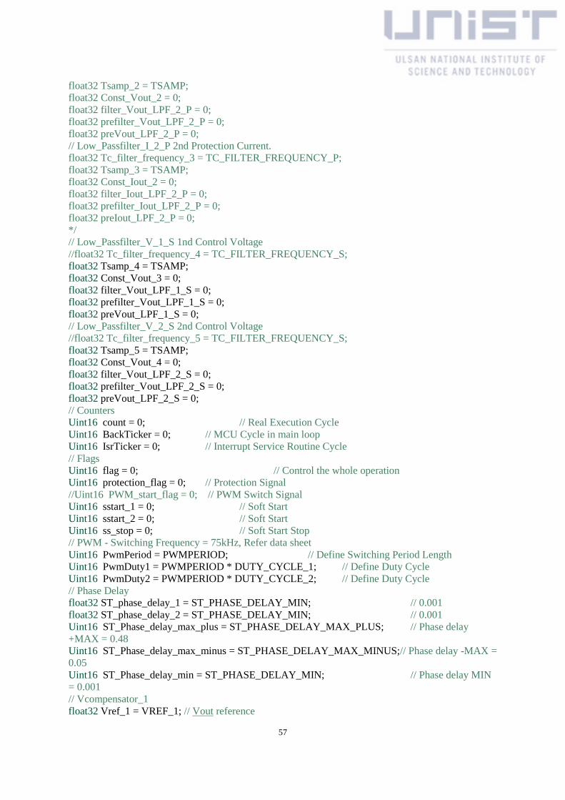
float32 Tsamp_2 = TSAMP; float32 Const_Vout_2 = 0; float32 filter_Vout_LPF_2_P = 0; float32 prefilter_Vout_LPF_2_P = 0; float32 preVout_LPF_2_P = 0; // Low_Passfilter_I_2_P 2nd Protection Current. float32 Tc_filter_frequency_3 = TC_FILTER_FREQUENCY_P; float32 Tsamp_3 = TSAMP; float32 Const_Iout_2 = 0; float32 filter_Iout_LPF_2_P = 0; float32 prefilter_Iout_LPF_2_P = 0; float32 preIout_LPF_2_P = 0; */ // Low_Passfilter_V_1_S 1nd Control Voltage //float32 Tc_filter_frequency_4 = TC_FILTER_FREQUENCY_S; float32 Tsamp_4 = TSAMP; float32 Const_Vout_3 = 0; float32 filter_Vout_LPF_1_S = 0; float32 prefilter_Vout_LPF_1_S = 0; float32 preVout_LPF_1_S = 0; // Low_Passfilter_V_2_S 2nd Control Voltage //float32 Tc_filter_frequency_5 = TC_FILTER_FREQUENCY_S; float32 Tsamp_5 = TSAMP; float32 Const_Vout_4 = 0; float32 filter_Vout_LPF_2_S = 0; float32 prefilter_Vout_LPF_2_S = 0; float32 preVout_LPF_2_S = 0; // Counters Uint16 count = 0; // Real Execution Cycle Uint16 BackTicker = 0; // MCU Cycle in main loop Uint16 IsrTicker = 0; // Interrupt Service Routine Cycle // Flags Uint16 flag = 0; // Control the whole operation Uint16 protection_flag = 0; // Protection Signal //Uint16 PWM_start_flag = 0; // PWM Switch Signal Uint16 sstart_1 = 0; // Soft Start Uint16 sstart_2 = 0; // Soft Start Uint16 ss_stop = 0; // Soft Start Stop // PWM - Switching Frequency = 75kHz, Refer data sheet Uint16 PwmPeriod = PWMPERIOD; // Define Switching Period Length Uint16 PwmDuty1 = PWMPERIOD * DUTY_CYCLE_1; // Define Duty Cycle Uint16 PwmDuty2 = PWMPERIOD * DUTY_CYCLE_2; // Define Duty Cycle // Phase Delay float32 ST_phase_delay_1 = ST_PHASE_DELAY_MIN; // 0.001 float32 ST_phase_delay_2 = ST_PHASE_DELAY_MIN; // 0.001 Uint16 ST_Phase_delay_max_plus = ST_PHASE_DELAY_MAX_PLUS; // Phase delay +MAX = 0.48 Uint16 ST_Phase_delay_max_minus = ST_PHASE_DELAY_MAX_MINUS;// Phase delay -MAX = 0.05 Uint16 ST_Phase_delay_min = ST_PHASE_DELAY_MIN; // Phase delay MIN = 0.001 // Vcompensator_1 float32 Vref_1 = VREF_1; // Vout reference
57

float32 V_Pg_1 = V_PG; // Initialize Weight : Pgain 5 float32 V_Ig_1 = V_IG; // Initialize Weight : Igain change to this from 0.03 float32 V_Dg_1 = V_DG; // Initialize Weight : Dgain float32 Verr_1 = 0; float32 V_Pgain_1 = 0; float32 V_Igain_1 = 0; float32 V_Dgain_1 = 0; float32 V_Igainp_1 = 0; float32 V_Ep_1 = 0; float32 V_PIDgain_1 = 0; // Vcompensator_2 float32 Vref_2 = VREF_2; // Vin Reference float32 V_Pg_2 = V_PG; // Initialize Weight : Pgain 5 float32 V_Ig_2 = V_IG; // Initialize Weight : Igain change to this from 0.03 float32 V_Dg_2 = V_DG; // Initialize Weight : Dgain float32 Verr_2 = 0; float32 V_Pgain_2 = 0; float32 V_Igain_2 = 0; float32 V_Dgain_2 = 0; float32 V_Igainp_2 = 0; float32 V_Ep_2 = 0; float32 V_PIDgain_2 = 0; /* // Icompensator_1 float32 Iref_1 = IREF_1; // Compare Iout = 250 with Reference float32 I_Pg_1 = I_PG; // Pgain float32 I_Ig_1 = I_IG; // Igain float32 Ierr_1 = 0; float32 I_Pgain_1 = 0; float32 I_Igain_1 = 0; float32 I_Igainp_1 = 0; float32 I_Ep_1 = 0; float32 I_PIgain_1 = 0; // Icompensator_2 float32 Iref_2 = IREF_2; // Compare Iout = 250 with Reference float32 I_Pg_2 = I_PG; // Pgain float32 I_Ig_2 = I_IG; // Igain float32 Ierr_2 = 0; float32 I_Pgain_2 = 0; float32 I_Igain_2 = 0; float32 I_Igainp_2 = 0; float32 I_Ep_2 = 0; float32 I_PIgain_2 = 0; */ /*************************************************************************** Function : Main Input : None Output : None Description - Initialize the whole things for DSP unit - Copy Code to RAM which is located in DSP unit - Iterate forever
58

****************************************************************************/ void main(void) { // Disable Global Interrupt DINT; // Clear Interrupt Flag IER = 0x0000; IFR = 0x0000; /* Initializes the System Control registers to a known state */ InitSysCtrl(); /* Gpio 0,1 set to PWM Output */ InitEPwm1Gpio(); // Initialize Peripheral Interrupt Expansion circuit InitPieCtrl(); // Pie Vector Table Re-allocation InitPieVectTable(); // Interrupt Service Routine Re-mapping EALLOW; // Write some value on Protected Map Area // Main Interrupt Service Routine allocates to ADC interrupt PieVectTable.ADCINT = &MainISR; // GPAMUX - 0 : General IO Port, 1 : PIE Connection GpioCtrlRegs.GPAMUX1.bit.GPIO10 = 0; GpioCtrlRegs.GPAMUX2.bit.GPIO24 = 0; GpioCtrlRegs.GPAMUX2.bit.GPIO25 = 0; // GpioCtrlRegs.GPAMUX2.bit.GPIO26 = 0; // GpioCtrlRegs.GPAMUX2.bit.GPIO27 = 0; // GPADIR - 0 : Input, 1 : Output GpioCtrlRegs.GPADIR.bit.GPIO10 = 0; // RelayOn pin - Start switch signal GpioCtrlRegs.GPADIR.bit.GPIO24 = 1; // UD1A - Dual Flip Flop Data - PWM3A,B GpioCtrlRegs.GPADIR.bit.GPIO25 = 1; // UD1B - Dual Flip Flop Data - PWM4A,B // GpioCtrlRegs.GPADIR.bit.GPIO26 = 1; // 1st pin - 2.54 Connector beside MCU // GpioCtrlRegs.GPADIR.bit.GPIO27 = 1; // 2nd pin - 2.54 Connector beside MCU // Re-Protect Memory Map Area EDIS; /* Enable PIE group 1 interrupt 6 for ADCINT */ PieCtrlRegs.PIEIER1.bit.INTx6 = 1; /* Enable CPU INT1 for ADCINT */ GpioDataRegs.GPACLEAR.bit.GPIO10 = 1; // Start switch signal clear GpioDataRegs.GPACLEAR.bit.GPIO24 = 1; // PWM3A,B Clear GpioDataRegs.GPACLEAR.bit.GPIO25 = 1; // PWM4A,B Clear // GpioDataRegs.GPACLEAR.bit.GPIO26 = 1; // GpioDataRegs.GPACLEAR.bit.GPIO27 = 1;
59

// GpioDataRegs.GPADAT.bit.GPIO26 = 1; // for checking the signal // Enable CPU INT1 for ADC interrupt IER |= M_INT1; // OR Bit Operator // Initialize Peripherals for User Application //#ifdef _FLASH // Copy Code to RAM MemCopy(&RamfuncsLoadStart, &RamfuncsLoadEnd, &RamfuncsRunStart); // Initialize Flash InitFlash(); //#endif // Initialize PWM InitEPwmModules(PwmPeriod); /* Initialize ADC module */ InitAdc(); /* Configure ADC */ // ADCCLK = HSPCLK/(ADCCLKPS*2)/(CPS+1) AdcRegs.ADCTRL3.bit.ADCCLKPS = 15; /* Pre-scaled HSPCLK = HSPCLK/(ADCCLKPS*2) */ AdcRegs.ADCTRL1.bit.CPS = 0; /* ADCCLK = Pre-scaled HSPCLK/CPS(+1) = 2.5MHz */ AdcRegs.ADCMAXCONV.all = 0x0003; /* Setup 1 conv's on SEQ1, accept ADC one time */ AdcRegs.ADCCHSELSEQ1.all = 0x98A1; /* VDC_Link = ADCINA1 */ AdcRegs.ADCTRL2.bit.EPWM_SOCA_SEQ1 = 1; /* Enable SOCA from ePWM to start SEQ1 */ AdcRegs.ADCTRL2.bit.INT_ENA_SEQ1 = 1; /* Enable SEQ1 interrupt (every EOS) */ /* Assumes ePWM1 clock is already enabled in InitSysCtrl(); */ EPwm1Regs.ETSEL.bit.SOCAEN = 1; /* Enable SOC on A group */ EPwm1Regs.ETSEL.bit.SOCASEL = 2; /* Select SOC from CNTR=PRD */ EPwm1Regs.ETPS.bit.SOCAPRD = 1; /* Generate pulse on 1st event */ ERTM; /* Enable Global real-time interrupt DBGM */ EINT; /* Enable Global interrupt INTM */ // train DBN Init_DBN(); /* IDLE loop. Just sit and loop forever: */ for(;;) { BackTicker++; // Iterate Loop Counter } } /*************************************************************************** Function : MainISR Input : None
60
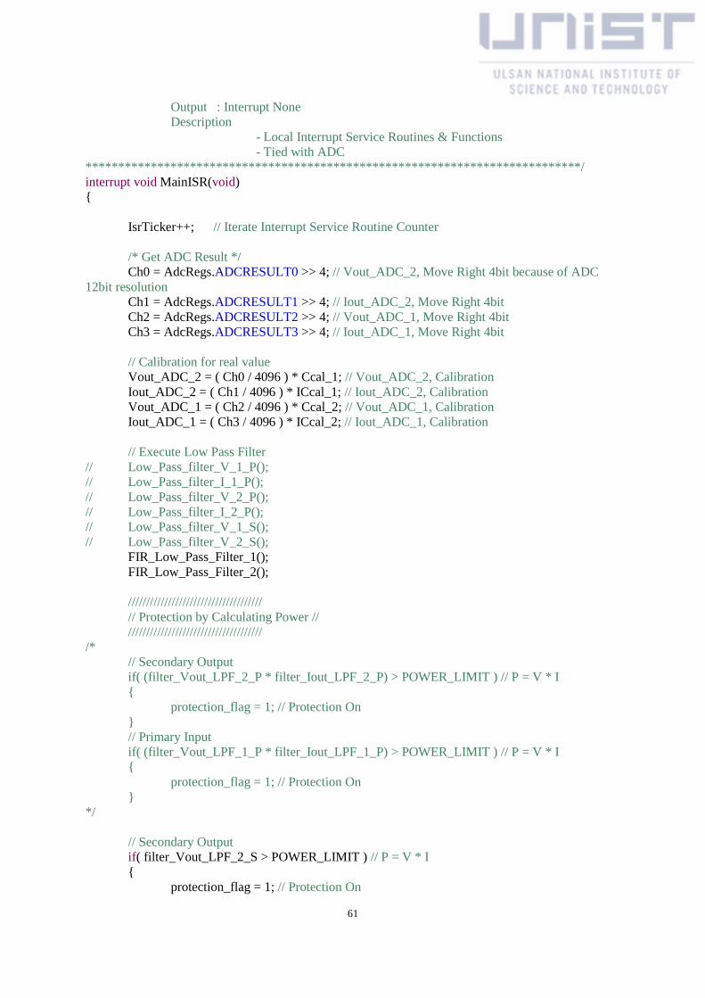
Output : Interrupt None Description - Local Interrupt Service Routines & Functions - Tied with ADC ****************************************************************************/ interrupt void MainISR(void) { IsrTicker++; // Iterate Interrupt Service Routine Counter /* Get ADC Result */ Ch0 = AdcRegs.ADCRESULT0 >> 4; // Vout_ADC_2, Move Right 4bit because of ADC 12bit resolution Ch1 = AdcRegs.ADCRESULT1 >> 4; // Iout_ADC_2, Move Right 4bit Ch2 = AdcRegs.ADCRESULT2 >> 4; // Vout_ADC_1, Move Right 4bit Ch3 = AdcRegs.ADCRESULT3 >> 4; // Iout_ADC_1, Move Right 4bit // Calibration for real value Vout_ADC_2 = ( Ch0 / 4096 ) * Ccal_1; // Vout_ADC_2, Calibration Iout_ADC_2 = ( Ch1 / 4096 ) * ICcal_1; // Iout_ADC_2, Calibration Vout_ADC_1 = ( Ch2 / 4096 ) * Ccal_2; // Vout_ADC_1, Calibration Iout_ADC_1 = ( Ch3 / 4096 ) * ICcal_2; // Iout_ADC_1, Calibration // Execute Low Pass Filter // Low_Pass_filter_V_1_P(); // Low_Pass_filter_I_1_P(); // Low_Pass_filter_V_2_P(); // Low_Pass_filter_I_2_P(); // Low_Pass_filter_V_1_S(); // Low_Pass_filter_V_2_S(); FIR_Low_Pass_Filter_1(); FIR_Low_Pass_Filter_2(); ///////////////////////////////////// // Protection by Calculating Power // ///////////////////////////////////// /* // Secondary Output if( (filter_Vout_LPF_2_P * filter_Iout_LPF_2_P) > POWER_LIMIT ) // P = V * I { protection_flag = 1; // Protection On } // Primary Input if( (filter_Vout_LPF_1_P * filter_Iout_LPF_1_P) > POWER_LIMIT ) // P = V * I { protection_flag = 1; // Protection On } */ // Secondary Output if( filter_Vout_LPF_2_S > POWER_LIMIT ) // P = V * I { protection_flag = 1; // Protection On
61

} // Primary Input if( filter_Vout_LPF_1_S > POWER_LIMIT ) // P = V * I { protection_flag = 1; // Protection On } // Clear the port of PWM3A,B and PWM4A,B GpioDataRegs.GPASET.bit.GPIO24 = 1; // PWM3A,B - 0:N/A 1:HIGH GpioDataRegs.GPASET.bit.GPIO25 = 1; // PWM4A,B - 0:N/A 1:HIGH /*********************************************** Start Switch Signal ************************************************/ // Start Switch Turn Off if(GpioDataRegs.GPADAT.bit.GPIO10 == 1) // Start Switch - 1:OFF, 0:ON { // Stop PWM signal PWM_stop_1(); PWM_stop_2(); // Initialize Value Init_Values(); } // Start Switch Turn On if(GpioDataRegs.GPADAT.bit.GPIO10 == 0 && protection_flag == 0) { if(flag == 2) // Start Switch Flag : Status 2 { ss_stop = 1; // Soft Start Stop Signal } flag = 1; // Start Switch Flag : Status 1 // Start PWM Signal PWM_start_1(); PWM_start_2(); PWM_Generation(); } // Start Control - Soft Start if(flag == 1) // Start Switch On { count++; // Soft Start softstart_1(); softstart_2(); if(sstart_1 == 1 && sstart_2 == 1) // Soft Start End {
62

flag = 2; dbn_flag = 0; // Init_DBN flag goes to Initial Condition } } // Soft Start Stop - Real Control if(flag == 2 && ss_stop == 1) { count++; ////////////////////////////////////// // Control Compensator // ////////////////////////////////////// Vcompensator_1(); // Voltage 1 Controller // Vcompensator_2(); // Voltage 2 Controller // Icompensator_1(); // Current 1 Controller // Icompensator_2(); // Current 2 Controller ////////////////////////////////////// // Phase Delay Update from Vout // ////////////////////////////////////// // Update Phase Delay if(V_PIDgain_1 >= 0) { EPwm4Regs.TBCTL.bit.PHSDIR = TB_DOWN; // TB_DOWN = 0 ST_phase_delay_1 = V_PIDgain_1; // Check Both Side Phase Limit if(ST_phase_delay_1 > ST_Phase_delay_max_plus) { ST_phase_delay_1 = ST_Phase_delay_max_plus; } if(ST_phase_delay_1 < ST_Phase_delay_min) { ST_phase_delay_1 = ST_Phase_delay_min; } } // Update Phase Delay if(V_PIDgain_1 < 0) { EPwm4Regs.TBCTL.bit.PHSDIR = TB_UP; // TB_UP = 1 V_PIDgain_1 = -V_PIDgain_1; ST_phase_delay_1 = V_PIDgain_1; // Check Both Side Phase Limit if(ST_phase_delay_1 > ST_Phase_delay_max_minus) { ST_phase_delay_1 = ST_Phase_delay_max_minus; } if(ST_phase_delay_1 < ST_Phase_delay_min)
63

{ ST_phase_delay_1 = ST_Phase_delay_min; } } ////////////////////////////////////// // Phase Delay Update from Vin // ////////////////////////////////////// // Update Phase Delay if(V_PIDgain_2 >= 0) { EPwm2Regs.TBCTL.bit.PHSDIR = TB_DOWN; ST_phase_delay_2 = V_PIDgain_2; // Check Both Side Phase Limit if(ST_phase_delay_2 > ST_Phase_delay_max_plus) { ST_phase_delay_2 = ST_Phase_delay_max_plus; } if(ST_phase_delay_2 < ST_Phase_delay_min) { ST_phase_delay_2 = ST_Phase_delay_min; } } // Update Phase Delay if(V_PIDgain_2 < 0) { EPwm2Regs.TBCTL.bit.PHSDIR = TB_UP; V_PIDgain_2 = -V_PIDgain_2; ST_phase_delay_2 = V_PIDgain_2; // Check Both Side Phase Limit if(ST_phase_delay_2 > ST_Phase_delay_max_minus) { ST_phase_delay_2 = ST_Phase_delay_max_minus; } if(ST_phase_delay_2 < ST_Phase_delay_min) { ST_phase_delay_2 = ST_Phase_delay_min; } } } // Protection Mode if(protection_flag == 1) { //GpioDataRegs.GPADAT.bit.GPIO26 = 1; GpioDataRegs.GPACLEAR.bit.GPIO24 = 1; GpioDataRegs.GPACLEAR.bit.GPIO25 = 1; PWM_stop_1(); PWM_stop_2();
64

} // Count and Retrain DBN if(count == 65535){ time1++; // 0.4396 sec if((time1 % 10) == 0){ DBNcompensator(); } if(time1 == 65535){ time2++; // 477.204025 min = about 8 hour if(time2 == 65535){ time3++; // 521226.09630625 hour = 21717.75 day } } } /* Reinitialize for next ADC sequence */ EPwm1Regs.ETCLR.bit.INT = 1; /* Enable More interrupt */ AdcRegs.ADCTRL2.bit.RST_SEQ1 = 1; /* Reset SEQ1 */ AdcRegs.ADCST.bit.INT_SEQ1_CLR = 1; /* Clear INT SEQ1 bit */ PieCtrlRegs.PIEACK.bit.ACK1 = 1; /* Acknowledge interrupt to PIE */ } /*************************************************************************** Function : Vcompensator1, Vcompensator2 - Regulated by Voltage Icompensator1, Icompensator2 - Regulated by Current Input : None Output : None Description - Calculate Compensator ****************************************************************************/ int a = 0; double b = 0; double Ku = 0; // DBN Compensator void DBNcompensator(void) { int i; // Fix the Value from one point value if(filter_Vout_LPF_2_S > Vref_1) test[2] = -1; // 0:down if(filter_Vout_LPF_2_S == Vref_1) test[2] = 0; // 1:stay if(filter_Vout_LPF_2_S < Vref_1) test[2] = 1; // 2:up // fix // if(Vout_ADC_2 > Vref_1) test[2] = -1; // 0:down // if(Vout_ADC_2 == Vref_1) test[2] = 0; // 1:stay // if(Vout_ADC_2 < Vref_1) test[2] = 1; // 2:up // Initialize Value result[0] = 0; result[1] = 0; result[2] = 0;
65

max = 0; max_flag = 0; // DBN Prediction DBN_predict(dbn, test, result); // Find Max Value for(i=0; i < dbn->n_outs; i++){ if(max < result[i]){ max = result[i]; max_flag = i; // 0:down, 1:stay, 2:up } Ku = Ku + (result[i] * (i-1)); if(Ku > 5) Ku = 5; if(Ku < -5) Ku = -5; } max_flag--; // -1:down, 0:stay, 1:up a = max_flag; b = max; // Calculate Gain P V_Pg_1 = V_Pg_1 + (Ku * 0.045); // delt Pgain = Wp * Ku if(V_Pg_1 > 1) V_Pg_1 = 1; if(V_Pg_1 <= 0) V_Pg_1 = 0.00001; // Calculate Gain I V_Ig_1 = V_Ig_1 + (Ku * 0.005); // delt Ggain = Wp * Ku if(V_Ig_1 > 20) V_Ig_1 = 20; if(V_Ig_1 <= 0) V_Ig_1 = 0.00001; } // Vout void Vcompensator_1(void) { // Calculate Error Verr_1 = Vref_1 - filter_Vout_LPF_2_S; // Vout_ADC_2 // Calculate PID V_Pgain_1 = Verr_1 * V_Pg_1; // P V_Igain_1 = V_Igainp_1 + (Verr_1 * V_Ig_1); // I V_Dgain_1 = (Verr_1 - V_Ep_1) * V_Dg_1; // D // Limit the Gain Value for Overthrowing if(V_Igain_1 > V_IGAIN_LIMIT) { V_Igain_1 = V_IGAIN_LIMIT; } if(V_Igain_1 < -V_IGAIN_LIMIT) { V_Igain_1 = -V_IGAIN_LIMIT; } // Limit the D Gain for Dead Zone if(fabs(Verr_1 - V_Ep_1) < V_DGAIN_LIMIT ) { V_Dgain_1 = 0;
66

} // Change Gain V_Igainp_1 = V_Igain_1; V_Ep_1 = Verr_1; V_PIDgain_1 = (V_Pgain_1 + V_Igain_1 + V_Dgain_1); // P+I+D } /* // Vin void Vcompensator_2(void) { // Calculate Error Verr_2 = Vref_2 - filter_Vout_LPF_1_S; // Vout_ADC_1 // Calculate Gain V_Pgain_2 = Verr_2 * V_Pg_2; V_Igain_2 = V_Igainp_2 + (Verr_2 * V_Ig_2); // Limit the Gain Value for Overthrowing if(V_Igain_2 > V_IGAIN_LIMIT) { V_Igain_2 = V_IGAIN_LIMIT; } if(V_Igain_2 < -V_IGAIN_LIMIT) { V_Igain_2 = -V_IGAIN_LIMIT; } // Change Gain V_Igainp_2 = V_Igain_2; V_PIDgain_2 = (V_Pgain_2 + V_Igain_2); } // Iin void Icompensator_1(void) { // Calculate Error Ierr_1 = Iref_1 - filter_Iout_LPF_1_P; // Iout_ADC_1 // Calculate Gain I_Pgain_1 = Ierr_1 * I_Pg_1; I_Igain_1 = I_Igainp_1 + (Ierr_1 * I_Ig_1); // Limit the I gain value for Overthrowing if(I_Igain_1 > I_IGAIN_LIMIT) { I_Igain_1 = I_IGAIN_LIMIT; } if(I_Igain_1 < -I_IGAIN_LIMIT) { I_Igain_1 = -I_IGAIN_LIMIT; } // Change PI Gain
67
I_PIgain_1 = (I_Pgain_1 + I_Igain_1); // Limit the PI gain value for Overthrowing if(I_PIgain_1 > I_PIGAIN_LIMIT) { I_PIgain_1 = I_PIGAIN_LIMIT; } if(I_PIgain_1 < -I_PIGAIN_LIMIT) { I_PIgain_1 = -I_PIGAIN_LIMIT; } // Change gain // PIgain = sqrt(PIgain * PIgain); I_Igainp_1 = I_Igain_1; I_Ep_1 = Ierr_1; } // Iout void Icompensator_2(void) { // Calculate Error Ierr_2 = Iref_2 - filter_Iout_LPF_2_P; // Iout_ADC_2 // Calculate Gain I_Pgain_2 = Ierr_2 * I_Pg_2; I_Igain_2 = I_Igainp_2 + (Ierr_2 * I_Ig_2); // Limit the I gain value for Overthrowing if(I_Igain_2 > I_IGAIN_LIMIT) { I_Igain_2 = I_IGAIN_LIMIT; } if(I_Igain_2 < -I_IGAIN_LIMIT) { I_Igain_2 = -I_IGAIN_LIMIT; } // Change PI Gain I_PIgain_2 = (I_Pgain_2 + I_Igain_2); // Limit the PI gain value for Overthrowing if(I_PIgain_2 > I_PIGAIN_LIMIT) { I_PIgain_2 = I_PIGAIN_LIMIT; } if(I_PIgain_2 < -I_PIGAIN_LIMIT) { I_PIgain_2 = -I_PIGAIN_LIMIT; } // Change gain // PIgain = sqrt(PIgain * PIgain); I_Igainp_2 = I_Igain_2; I_Ep_2 = Ierr_2; } */ /*************************************************************************** Function : softstart_1, softstart_2
68

Input : None Output : None Description - Soft Start Switching ****************************************************************************/ // Soft Start for Input void softstart_1(void) { // Increase Soft Start ST_phase_delay_1 = ST_phase_delay_1 + ST_PHASE_RATE; // 0.005 // 0.1 //GpioDataRegs.GPADAT.bit.GPIO26 = 0; // Finish Soft Start if( ST_phase_delay_1 >= ST_PHASE_DELAY_MAX_PLUS || filter_Vout_LPF_2_S >= Vref_1 ) // Regulated by Phase and Voltage : other option - current { sstart_1 = 1; // 0:Start, 1:Finish //GpioDataRegs.GPADAT.bit.GPIO26 = 1; //DELAY_US(1000000); } } // Soft Start for Output void softstart_2(void) { // Increase Soft Start ST_phase_delay_2 = ST_phase_delay_2 + ST_PHASE_RATE; // 0.005 // 0.1 //GpioDataRegs.GPADAT.bit.GPIO26 = 0; // Finish Soft Start if( ST_phase_delay_2 >= ST_PHASE_DELAY_MAX_PLUS || filter_Vout_LPF_1_S >= Vref_2 ) // Regulated by Phase and Voltage : other option - current { sstart_2 = 1; // 0:Start, 1:Finish //GpioDataRegs.GPADAT.bit.GPIO26 = 1; //DELAY_US(1000000); } } /*************************************************************************** Function : Low_Pass_filter_V_1_P, Low_Pass_filter_I_1_P Low_Pass_filter_V_2_P, Low_Pass_filter_I_2_P Low_Pass_filter_V_1_S, Low_Pass_filter_V_2_S Input : None Output : None Description - Calculate 1st Order Low Pass Filter ****************************************************************************/ /* // Primary Voltage void Low_Pass_filter_V_1_P(void) {
69

// Calculation Const_Vout_1 = Tsamp / (Tsamp + 2 * Tc_filter_frequency); filter_Vout_LPF_1_P = prefilter_Vout_LPF_1_P + Const_Vout_1 * (Vout_ADC_1 + preVout_LPF_1_P - 2 * prefilter_Vout_LPF_1_P); // For next step, save the former value prefilter_Vout_LPF_1_P = filter_Vout_LPF_1_P; preVout_LPF_1_P = Vout_ADC_1; } // Primary I(Current) void Low_Pass_filter_I_1_P(void) { // Calculation Const_Iout_1 = Tsamp_1 / (Tsamp_1 + 2 * Tc_filter_frequency_1); filter_Iout_LPF_1_P = prefilter_Iout_LPF_1_P + Const_Iout_1 * (Iout_ADC_1 + preIout_LPF_1_P - 2 * prefilter_Iout_LPF_1_P); // For next step, save the former value prefilter_Iout_LPF_1_P = filter_Iout_LPF_1_P; preIout_LPF_1_P = Iout_ADC_1; } // Secondary Voltage void Low_Pass_filter_V_2_P(void) { // Calculation Const_Vout_2 = Tsamp_2 / (Tsamp_2 + 2 * Tc_filter_frequency_2); filter_Vout_LPF_2_P = prefilter_Vout_LPF_2_P + Const_Vout_2 * (Vout_ADC_2 + preVout_LPF_2_P - 2 * prefilter_Vout_LPF_2_P); // For next step, save the former value prefilter_Vout_LPF_2_P = filter_Vout_LPF_2_P; preVout_LPF_2_P = Vout_ADC_2; } // Secondary I(Current) void Low_Pass_filter_I_2_P(void) { // Calculation Const_Iout_2 = Tsamp_3 / (Tsamp_3 + 2 * Tc_filter_frequency_3); filter_Iout_LPF_2_P = prefilter_Iout_LPF_2_P + Const_Iout_2 * (Iout_ADC_2 + preIout_LPF_2_P - 2 * prefilter_Iout_LPF_2_P); // For next step, save the former value prefilter_Iout_LPF_2_P = filter_Iout_LPF_2_P; preIout_LPF_2_P = Iout_ADC_2; } // Vin // Updated but need to modify the values void Low_Pass_filter_V_1_S(void) { // Calculation Const_Vout_3 = Tsamp_4 / (Tsamp_4 + 2 * Tc_filter_frequency_4); filter_Vout_LPF_1_S = prefilter_Vout_LPF_1_S + Const_Vout_3 * (Vout_ADC_1 + preVout_LPF_1_S - 2 * prefilter_Vout_LPF_1_S); // For next step, save the former value
70

prefilter_Vout_LPF_1_S = filter_Vout_LPF_1_S; preVout_LPF_1_S = Vout_ADC_1; } // Vout void Low_Pass_filter_V_2_S(void) { // Calculation - frequency 20kHz Const_Vout_4 = Tsamp_5 / (Tsamp_5 + 2 * Tc_filter_frequency_5); filter_Vout_LPF_2_S = prefilter_Vout_LPF_2_S + Const_Vout_4 * (Vout_ADC_2 + preVout_LPF_2_S - 2 * prefilter_Vout_LPF_2_S); // For next step, save the former value prefilter_Vout_LPF_2_S = filter_Vout_LPF_2_S; preVout_LPF_2_S = Vout_ADC_2; } */ // Input Part void FIR_Low_Pass_Filter_1(void) { int i; double sum = 0; // Initialize Sum // Input the Newest Value // input[0] = 0.03225806451612903225 * Vout_ADC_2; input_1[0] = Vout_ADC_1; // Calculate Finite Impulse Response Filter - Low Pass for(i=30; i>=0; i--){ sum += (h[i] * input_1[i]); // Calculation input_1[i+1] = input_1[i]; // Move Samples } // Update FIR Low Pass Filter Value filter_Vout_LPF_1_S = sum; } // Output Part void FIR_Low_Pass_Filter_2(void) { int i; double sum = 0; // Initialize Sum // Input the Newest Value // input[0] = 0.03225806451612903225 * Vout_ADC_2; input_2[0] = Vout_ADC_2; // Calculate Finite Impulse Response Filter - Low Pass for(i=30; i>=0; i--){ sum += (h[i] * input_2[i]); // Calculation input_2[i+1] = input_2[i]; // Move Samples } // Update FIR Low Pass Filter Value filter_Vout_LPF_2_S = sum; } /*************************************************************************** Function : PWM_stop_1, PWM_start_1, PWM_stop_2, PWM_start_2 PWM_Generation
71

Input : None Output : None Description - Control PWM Signal ****************************************************************************/ // Start PWM1 void PWM_start_1() // All PWM signal start { EPwm1Regs.AQSFRC.bit.RLDCSF = 0; EPwm1Regs.AQSFRC.bit.ACTSFA = 0; EPwm1Regs.AQSFRC.bit.ACTSFB = 0; EPwm1Regs.AQSFRC.bit.OTSFA = 0; EPwm1Regs.AQSFRC.bit.OTSFB = 0; EPwm1Regs.AQCSFRC.bit.CSFA = 0; EPwm1Regs.AQCSFRC.bit.CSFB = 1; EPwm1Regs.DBCTL.bit.OUT_MODE = 3; EPwm2Regs.AQSFRC.bit.RLDCSF = 0; EPwm2Regs.AQSFRC.bit.ACTSFA = 0; EPwm2Regs.AQSFRC.bit.ACTSFB = 0; EPwm2Regs.AQSFRC.bit.OTSFA = 0; EPwm2Regs.AQSFRC.bit.OTSFB = 0; EPwm2Regs.AQCSFRC.bit.CSFA = 0; EPwm2Regs.AQCSFRC.bit.CSFB = 1; EPwm2Regs.DBCTL.bit.OUT_MODE = 3; } // Start PWM2 void PWM_start_2() { EPwm3Regs.AQSFRC.bit.RLDCSF = 0; EPwm3Regs.AQSFRC.bit.ACTSFA = 0; EPwm3Regs.AQSFRC.bit.ACTSFB = 0; EPwm3Regs.AQSFRC.bit.OTSFA = 0; EPwm3Regs.AQSFRC.bit.OTSFB = 0; EPwm3Regs.AQCSFRC.bit.CSFA = 0; EPwm3Regs.AQCSFRC.bit.CSFB = 1; EPwm3Regs.DBCTL.bit.OUT_MODE = 3; EPwm4Regs.AQSFRC.bit.RLDCSF = 0; EPwm4Regs.AQSFRC.bit.ACTSFA = 0; EPwm4Regs.AQSFRC.bit.ACTSFB = 0; EPwm4Regs.AQSFRC.bit.OTSFA = 0; EPwm4Regs.AQSFRC.bit.OTSFB = 0; EPwm4Regs.AQCSFRC.bit.CSFA = 0; EPwm4Regs.AQCSFRC.bit.CSFB = 1; EPwm4Regs.DBCTL.bit.OUT_MODE = 3; } // Stop PWM1 void PWM_stop_1() // All PWM signal stop { EPwm1Regs.AQSFRC.bit.RLDCSF = 3; EPwm1Regs.AQSFRC.bit.ACTSFA = 1;
72

EPwm1Regs.AQSFRC.bit.ACTSFB = 1; EPwm1Regs.AQSFRC.bit.OTSFA = 1; EPwm1Regs.AQSFRC.bit.OTSFB = 1; EPwm1Regs.AQCSFRC.bit.CSFA = 1; EPwm1Regs.AQCSFRC.bit.CSFB = 1; EPwm1Regs.DBCTL.bit.OUT_MODE = 0; EPwm2Regs.AQSFRC.bit.RLDCSF = 3; EPwm2Regs.AQSFRC.bit.ACTSFA = 1; EPwm2Regs.AQSFRC.bit.ACTSFB = 1; EPwm2Regs.AQSFRC.bit.OTSFA = 1; EPwm2Regs.AQSFRC.bit.OTSFB = 1; EPwm2Regs.AQCSFRC.bit.CSFA = 1; EPwm2Regs.AQCSFRC.bit.CSFB = 1; EPwm2Regs.DBCTL.bit.OUT_MODE = 0; } // Stop PWM2 void PWM_stop_2() { EPwm3Regs.AQSFRC.bit.RLDCSF = 3; EPwm3Regs.AQSFRC.bit.ACTSFA = 1; EPwm3Regs.AQSFRC.bit.ACTSFB = 1; EPwm3Regs.AQSFRC.bit.OTSFA = 1; EPwm3Regs.AQSFRC.bit.OTSFB = 1; EPwm3Regs.AQCSFRC.bit.CSFA = 1; EPwm3Regs.AQCSFRC.bit.CSFB = 1; EPwm3Regs.DBCTL.bit.OUT_MODE = 0; EPwm4Regs.AQSFRC.bit.RLDCSF = 3; EPwm4Regs.AQSFRC.bit.ACTSFA = 1; EPwm4Regs.AQSFRC.bit.ACTSFB = 1; EPwm4Regs.AQSFRC.bit.OTSFA = 1; EPwm4Regs.AQSFRC.bit.OTSFB = 1; EPwm4Regs.AQCSFRC.bit.CSFA = 1; EPwm4Regs.AQCSFRC.bit.CSFB = 1; EPwm4Regs.DBCTL.bit.OUT_MODE = 0; } // Generate PWM void PWM_Generation() { /********************************************* * Need to Update this part for evaluation *********************************************/ /* Update EPWM's CMPA registers */ EPwm1Regs.TBPRD = PwmPeriod; EPwm1Regs.CMPA.half.CMPA = PwmDuty2; EPwm1Regs.TBPHS.half.TBPHS = PwmPeriod * (ST_phase_delay_2 / ST_PHASE_DELAY_PERIOD); // Phase Delay EPwm2Regs.TBPRD = PwmPeriod; EPwm2Regs.CMPA.half.CMPA = PwmDuty1; /*********************************************
73

* Original Code, Compare with upper code *********************************************/ /* Update EPWM's CMPA registers */ EPwm3Regs.TBPRD = PwmPeriod; // Phase Period EPwm3Regs.CMPA.half.CMPA = PwmDuty1; EPwm4Regs.TBPRD = PwmPeriod; // Phase Period EPwm4Regs.CMPA.half.CMPA = PwmDuty2; EPwm4Regs.TBPHS.half.TBPHS = PwmPeriod * (ST_phase_delay_1 / ST_PHASE_DELAY_PERIOD); // Phase Shift Delay } /*************************************************************************** Function : Init_Values, InitEPWMModules Input : None Output : None, Uint16 Period Description - Initialize Values and EPWM Modules ****************************************************************************/ // Initialize Global Variables void Init_Values() { // Flags & Counters protection_flag = 0; // Protection Signal flag = 0; count = 0; sstart_1 = 0; // Soft Start sstart_2 = 0; // Soft Start ss_stop = 0; // Soft Start Stop // PWM PwmPeriod = PWMPERIOD; // Switching Frequency = 75kHz, Refer datasheet PwmDuty1 = PWMPERIOD * DUTY_CYCLE_1; // Define Duty Cycle PwmDuty2 = PWMPERIOD * DUTY_CYCLE_2; // Define Duty Cycle // Phase Delay ST_phase_delay_1 = ST_PHASE_DELAY_MIN; // 0.001 ST_phase_delay_2 = ST_PHASE_DELAY_MIN; // 0.001 // Vcompensator1 Verr_1 = 0; V_Pgain_1 = 0; V_Igain_1 = 0; V_Dgain_1 = 0; V_Igainp_1 = 0; V_Ep_1 = 0; V_PIDgain_1 = 0; // Vcompensator2 Verr_2 = 0; V_Pgain_2 = 0; V_Igain_2 = 0; V_Dgain_2 = 0; V_Igainp_2 = 0; V_Ep_2 = 0; V_PIDgain_2 = 0; /*
74

// Icompensator1 Ierr_1 = 0; I_Pgain_1 = 0; I_Igain_1 = 0; I_Igainp_1 = 0; I_Ep_1 = 0; I_PIgain_1 = 0; // Icompensator2 Ierr_2 = 0; I_Pgain_2 = 0; I_Igain_2 = 0; I_Igainp_2 = 0; I_Ep_2 = 0; I_PIgain_2 = 0; */ // Initialize DBN values test[0] = 0; test[1] = 0; test[2] = 0; test[3] = 0; test1[0] = 0; test1[1] = 0; test1[2] = 0; result[0] = 0; result[1] = 0; result[2] = 0; max = 0; max_flag = 0; Ku = 0; // Initialize DBN - just one time : too much computing cost for Init_dbn if(dbn_flag == 0){ DBN__destruct(dbn); free(dbn); Init_DBN(); dbn_flag = 1; } } // Initialize EPWM Modules void InitEPwmModules(Uint16 Period) { EALLOW; SysCtrlRegs.PCLKCR0.bit.TBCLKSYNC = 0; EDIS; // ===================[ EPWM Module1 config ]=================== /* Setup TBCLK */ EPwm1Regs.TBPRD = Period; //* Set timer period EPwm1Regs.TBPHS.half.TBPHS = 0x0000; //* Phase is 0 EPwm1Regs.TBCTR = 0x0000; //* Clear counter /* Set Compare values */ EPwm1Regs.CMPA.half.CMPA = Period * 0.5;//* Set Compare A value EPwm1Regs.CMPB = 0; //* Set Compare B value /* Setup counter mode */ EPwm1Regs.TBCTL.bit.CTRMODE = 2; //* Count up/down (Symmetric) EPwm1Regs.TBCTL.bit.PHSEN = TB_DISABLE; //* Master - Disable phase loading EPwm1Regs.TBCTL.bit.HSPCLKDIV = 0; //* Clock ratio to SYSCLKOUT EPwm1Regs.TBCTL.bit.CLKDIV = 0; EPwm1Regs.TBCTL.bit.PRDLD = TB_SHADOW;
75

EPwm1Regs.TBCTL.bit.SYNCOSEL = TB_CTR_ZERO; // TB_CTR_ZERO //* Setup shadowing EPwm1Regs.CMPCTL.bit.SHDWAMODE = 0; //* Enable Shadowing EPwm1Regs.CMPCTL.bit.SHDWBMODE = 0; EPwm1Regs.CMPCTL.bit.LOADAMODE = 0; //* Load on CNTR=Zero EPwm1Regs.CMPCTL.bit.LOADBMODE = 0; //* Set actions EPwm1Regs.AQCTLA.bit.CAU = 2; //* Clear EPWM1A on event A, up count EPwm1Regs.AQCTLA.bit.CAD = 1; //* Set EPWM1A on event A, down count EPwm1Regs.AQCTLB.bit.CBU = 1; //* Clear EPWM1B on event B, up count EPwm1Regs.AQCTLB.bit.CBD = 2; //* Set EPWM1B on event B, down count EPwm1Regs.DBCTL.bit.OUT_MODE = 3; EPwm1Regs.DBCTL.bit.POLSEL = 2; EPwm1Regs.DBFED = 75; // PWM Down DeadTime EPwm1Regs.DBRED = 75; // PWM Up DeadTime // ===================[ EPWM Module2 config ]=================== //Setup TBCLK EPwm2Regs.TBPRD = Period; // Set timer period EPwm2Regs.TBPHS.half.TBPHS = 0x0000; // Phase is 0 EPwm2Regs.TBCTR = 0x0000; // Clear counter //Set Compare values EPwm2Regs.CMPA.half.CMPA = Period * 0.5; // Set Compare A value EPwm2Regs.CMPB = 0; //Set Compare B value // Setup counter mode EPwm2Regs.TBCTL.bit.CTRMODE = 2; // Count up/down (Symmetric) EPwm2Regs.TBCTL.bit.PHSEN = TB_ENABLE; // Slave - Enable phase loading EPwm2Regs.TBCTL.bit.PHSDIR = TB_DOWN; // Count DOWN on sync (=120 deg) EPwm2Regs.TBCTL.bit.HSPCLKDIV = 0; // Clock ratio to SYSCLKOUT EPwm2Regs.TBCTL.bit.CLKDIV = 0; EPwm2Regs.TBCTL.bit.PRDLD = TB_SHADOW; EPwm2Regs.TBCTL.bit.SYNCOSEL = TB_SYNC_IN; // TB_SYNC_IN // Setup shadowing EPwm2Regs.CMPCTL.bit.SHDWAMODE = 0; // Enable Shadowing EPwm2Regs.CMPCTL.bit.SHDWBMODE = 0; EPwm2Regs.CMPCTL.bit.LOADAMODE = 0; // Load on CNTR=Zero EPwm2Regs.CMPCTL.bit.LOADBMODE = 0; // Set actions EPwm2Regs.AQCTLA.bit.CAU = 2; // Clear EPWm2A on event A, up count EPwm2Regs.AQCTLA.bit.CAD = 1; // Set EPWm2A on event A, down count
76

EPwm2Regs.AQCTLB.bit.CBU = 1; // Clear EPWm2B on event B, up count EPwm2Regs.AQCTLB.bit.CBD = 2; // Set EPWm2B on event B, down count EPwm2Regs.DBCTL.bit.OUT_MODE = 3; EPwm2Regs.DBCTL.bit.POLSEL = 2; EPwm2Regs.DBFED = 75; // PWM Down DeadTime EPwm2Regs.DBRED = 75; // PWM Up DeadTime // ===================[ EPWM Module3 config ]=================== //Setup TBCLK EPwm3Regs.TBPRD = Period; // Set timer period EPwm3Regs.TBPHS.half.TBPHS = 0x0000; // Phase is 0 EPwm3Regs.TBCTR = 0x0000; // Clear counter //Set Compare values EPwm3Regs.CMPA.half.CMPA = Period * 0.5; // Set Compare A value EPwm3Regs.CMPB = 0; //Set Compare B value // Setup counter mode EPwm3Regs.TBCTL.bit.CTRMODE = 2; // Count up/down (Symmetric) EPwm3Regs.TBCTL.bit.PHSEN = TB_ENABLE; // Slave - Enable phase loading EPwm3Regs.TBCTL.bit.PHSDIR = TB_DOWN; // Count DOWN on sync (=120 deg) EPwm3Regs.TBCTL.bit.HSPCLKDIV = 0; //Clock ratio to SYSCLKOUT EPwm3Regs.TBCTL.bit.CLKDIV = 0; EPwm3Regs.TBCTL.bit.PRDLD = TB_SHADOW; EPwm3Regs.TBCTL.bit.SYNCOSEL = TB_SYNC_IN; // TB_SYNC_IN // Setup shadowing EPwm3Regs.CMPCTL.bit.SHDWAMODE = 0; // Enable Shadowing EPwm3Regs.CMPCTL.bit.SHDWBMODE = 0; EPwm3Regs.CMPCTL.bit.LOADAMODE = 0; // Load on CNTR=Zero EPwm3Regs.CMPCTL.bit.LOADBMODE = 0; // Set actions EPwm3Regs.AQCTLA.bit.CAU = 2; // Clear EPWm2A on event A, up count EPwm3Regs.AQCTLA.bit.CAD = 1; // Set EPWm2A on event A, down count EPwm3Regs.AQCTLB.bit.CBU = 1; // Clear EPWm2B on event B, up count EPwm3Regs.AQCTLB.bit.CBD = 2; // Set EPWm2B on event B, down count EPwm3Regs.DBCTL.bit.OUT_MODE = 3; EPwm3Regs.DBCTL.bit.POLSEL = 2; EPwm3Regs.DBFED = 75; // PWM Down DeadTime EPwm3Regs.DBRED = 75; // PWM Up DeadTime // ===================[ EPWM Module4 config ]=================== //Setup TBCLK EPwm4Regs.TBPRD = Period; // Set timer period EPwm4Regs.TBPHS.half.TBPHS = 0x0000; // Phase is 0
77

EPwm4Regs.TBCTR = 0x0000; // Clear counter //Set Compare values EPwm4Regs.CMPA.half.CMPA = Period*0.5; // Set Compare A value EPwm4Regs.CMPB = 0; //Set Compare B value // Setup counter mode EPwm4Regs.TBCTL.bit.CTRMODE = 2; // Count up/down (Symmetric) EPwm4Regs.TBCTL.bit.PHSEN = TB_ENABLE; // Slave - Enable phase loading EPwm4Regs.TBCTL.bit.PHSDIR = TB_DOWN; // Count DOWN on sync (=120 deg) EPwm4Regs.TBCTL.bit.HSPCLKDIV = 0; //Clock ratio to SYSCLKOUT EPwm4Regs.TBCTL.bit.CLKDIV = 0; EPwm4Regs.TBCTL.bit.PRDLD = TB_SHADOW; EPwm4Regs.TBCTL.bit.SYNCOSEL = TB_SYNC_IN; // TB_SYNC_IN // Setup shadowing EPwm4Regs.CMPCTL.bit.SHDWAMODE = 0; // Enable Shadowing EPwm4Regs.CMPCTL.bit.SHDWBMODE = 0; EPwm4Regs.CMPCTL.bit.LOADAMODE = 0; // Load on CNTR=Zero EPwm4Regs.CMPCTL.bit.LOADBMODE = 0; // Set actions EPwm4Regs.AQCTLA.bit.CAU = 2; // Clear EPWm2A on event A, up count EPwm4Regs.AQCTLA.bit.CAD = 1; //Set EPWm2A on event A, down count EPwm4Regs.AQCTLB.bit.CBU = 1; // Clear EPWm2B on event B, up count EPwm4Regs.AQCTLB.bit.CBD = 2; // Set EPWm2B on event B, down count EPwm4Regs.DBCTL.bit.OUT_MODE = 3; EPwm4Regs.DBCTL.bit.POLSEL = 2; EPwm4Regs.DBFED = 75; // PWM Down DeadTime EPwm4Regs.DBRED = 75; // PWM Up DeadTime EALLOW; SysCtrlRegs.PCLKCR0.bit.TBCLKSYNC = 1; // Setting six EPWM as primary output pins GpioCtrlRegs.GPAMUX1.bit.GPIO0 = 1; // EPWM1A pin GpioCtrlRegs.GPAMUX1.bit.GPIO1 = 1; // EPWM1B pin GpioCtrlRegs.GPAMUX1.bit.GPIO2 = 1; // EPWM2A pin GpioCtrlRegs.GPAMUX1.bit.GPIO3 = 1; // EPWM2B pin GpioCtrlRegs.GPAMUX1.bit.GPIO4 = 1; // EPWM3A pin GpioCtrlRegs.GPAMUX1.bit.GPIO5 = 1; // EPWM3B pin GpioCtrlRegs.GPAMUX1.bit.GPIO6 = 1; // EPWM4A pin GpioCtrlRegs.GPAMUX1.bit.GPIO7 = 1; // EPWM4B pin EDIS; } /*======================================================================
78

End of file. ======================================================================*/
79

Acknowledgement Kim, Sul Gi
Master of Science, Electrical and Computer Engineering, UNIST, 2011.9 ~ 2014.8. Jan. 2013. ~ Aug. 2014.
Advanced Power Interface and Power Electronics Lab., School of Electrical Engineering. Jan. 2012. ~ Dec. 2012.
Data Intensive Computing Lab., School of Computer Science and Engineering. Aug. 2011. ~ Dec. 2011.
Business Intelligence Lab., School of Technology Management. Academic Credit Earned
48 Credits / 3 Years Academic Activities 4 Domestic Conferences 1 Domestic Transaction 1 Domestic Journal 1 Domestic Company Competition Paper 1 Domestic Patent 1 International Journal 1 Degree Dissertation Academic Interests Optimization Theory, Control Theory, Artificial Intelligence, Machine Learning, Massive Data
Processing and Analysis, Distributed and Parallel Computing, Embedded System, Super Computing, GPGPU and Circuit Design.
Scholarship + Stipend
19,470,000 Won + 11,850,000 Won = 31,320,000 Won / 3 Years Living Spend (Housing, Foods, Etc.)
9,000,000 Won + 7,200,000 Won + 7,200,000 Won = 27,000,000 Won / 3Years Tuition Fee
15,572,000 Won / 3 Years Special Thanks to EA utd, Pinocchio, Kazakhstan Students, Ulsan Football Association and Many Others.
80