dld morris mano ch 6
TRANSCRIPT

Kayhan DURSUNKayhan DURSUN
Mantıksal Devre Tasarımı Dersi
6.Bölüm Cevapları6.Bölüm Cevapları

1Include a two input NAND gate with the register of Fig. 6-1 and connect the gate output to the C inputs of all flip-flops.One input of the NAND gate receives the clock pulses from the clock generator,and the other input of the NAND gate provides paralel load control.Explain the operation of the modified register.
A0I0 D
C
I1A1D
C
Clock Load Operation
X 0 No change
I2
Load
CLKA2
C
D
X 0 No change
0 1 No change
1 1 Load I2CLKA2D
C
1 1 Load
I3A3D
C

Load
2Include a synchronous clear input to the register of Fig 6.2.The modified register will have a parallel load capability and a synchronous clear capability.The register is cleared synchronously when the clock goes through a positive transition and the clear input is equal to 1.
A0
Load
ClearI
DI0 C
A1
I1
D
C
A2
C
D A2
I2Clear Load Operation
0 0 No change
1 0 0
D
C
A3
I
1 0 0
X 1 Load inputs
DI3
CLK
C

3 What is the difference between serial and parallel transfer?Explain how to convert serial data to parallel and parallel data to serial.
• Seri transferde bir saat vuruşunda yalnızca bir bit iletilirken,paralel • Seri transferde bir saat vuruşunda yalnızca bir bit iletilirken,paralel transferde bir saat vuruşu ile tüm bitler iletirlir.Bu nedenle seri transfer daha yavaştır ancak maliyeti de daha azdır.
• Seri transferi paralel transfere çevirmek için,ilk başta bütün bitler shift register ile tek tek aktarılıp çıkışlar paralel olarak bağlanır.shift register ile tek tek aktarılıp çıkışlar paralel olarak bağlanır.
• Paralel transferi seri transfere çevirmek için ise ilk başta veri paralel • Paralel transferi seri transfere çevirmek için ise ilk başta veri paralel yüklenip çıkışta bitler teker teker iletilir.

4The content of a 4-Bit register is initially 1101.The register is shifted six times to the right with the serial input being
101101.What is the content of the register after each shift?101101.What is the content of the register after each shift?
S.I=101101S.I=101101Initial 1.Shift 2.Shift 3.Shift 4.Shift 5.Shift 6.Shift
1101 1110 0111 1011 1101 0110 10111101 1110 0111 1011 1101 0110 1011
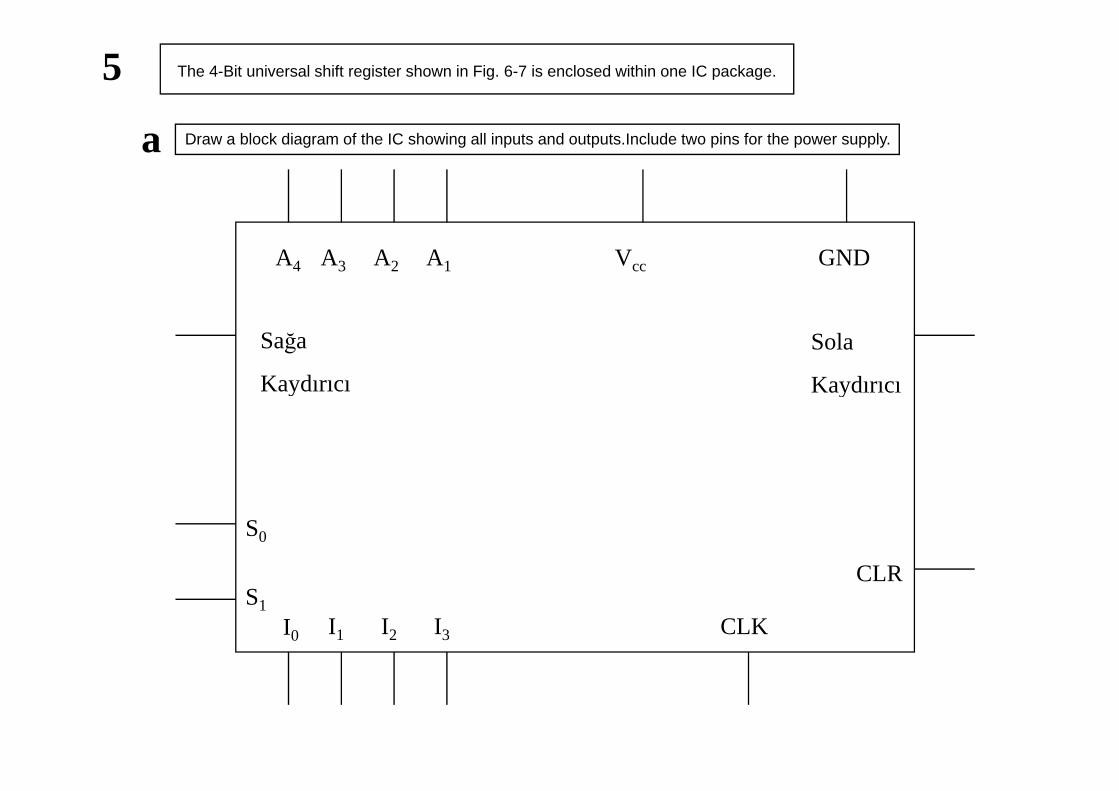
5
a
The 4-Bit universal shift register shown in Fig. 6-7 is enclosed within one IC package.
a Draw a block diagram of the IC showing all inputs and outputs.Include two pins for the power supply.
A4 A3 A2 A1 Vcc GND
Sağa
Kaydırıcı
Sola
KaydırıcıKaydırıcı Kaydırıcı
S0
CLRS1
CLR
I0 I1 I2 I3 CLK
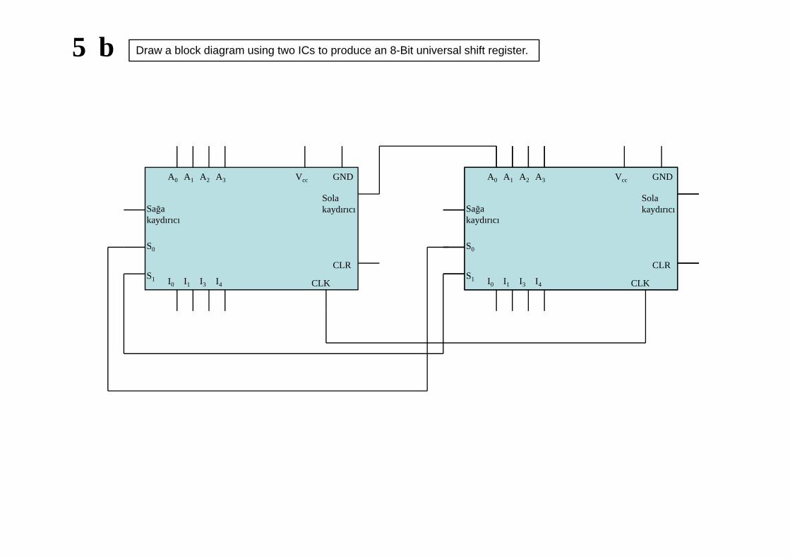
5 b Draw a block diagram using two ICs to produce an 8-Bit universal shift register.
Sağa kaydırıcı
A0 A1 A2 A3 Vcc GND
Sola kaydırıcı Sağa
kaydırıcı
A0 A1 A2 A3 Vcc GND
Sola kaydırıcı
kaydırıcı
S0
S1 I I I I
CLR
CLK
kaydırıcı
S0
S1 I I I I
CLR
CLKS1 I0 I1 I3 I4 CLK
S1 I0 I1 I3 I4 CLK

6
Design a 4 bit shift register with parallel load using D flip-flops.There are two control inputs:shift and load.When shift=1,the content of the register is shift by control inputs:shift and load.When shift=1,the content of the register is shift by one position.New data is transfered into the register when load =1 and shift=0.If both control inputs are equal to 0,the content of the register does not change. change.

Load
Shift
6
S.I.I0
D
CC
D
CI1
DD
CI2
DD
CI3

77
Draw the logic diagram of a 4-bit register with four D flip-flops and four 4x1 multiplexers with mode selection inputs s1 and s0.The register operates according to the following function table.according to the following function table.
s1 s0 Register Operation
0 0 No change0 0 No change
0 1 Complement the four outputs
1 0 Clear register to 0(synchronous with the clock)1 0 Clear register to 0(synchronous with the clock)
1 1 Load parallel data
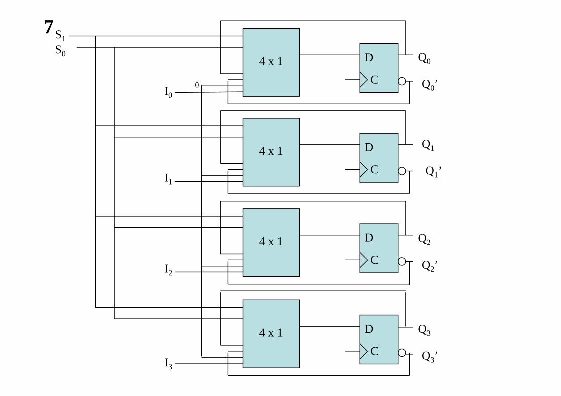
4 x 1 D
S1
S0 Q0
7
4 x 1 D
C0I0
Q0
Q0’
4 x 1 D Q14 x 1 D
CI1
Q1’
4 x 1 D Q24 x 1 D
CI2
Q2
Q2’
4 x 1 D Q34 x 1 D
CI3
Q3
Q3’
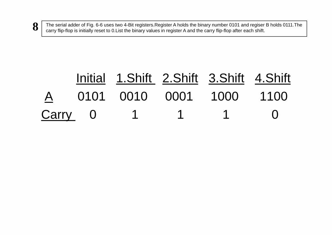
8 The serial adder of Fig. 6-6 uses two 4-Bit registers.Register A holds the binary number 0101 and regiser B holds 0111.The carry flip-flop is initially reset to 0.List the binary values in register A and the carry flip-flop after each shift.
Initial 1.Shift 2.Shift 3.Shift 4.ShiftA 0101 0010 0001 1000 1100A 0101 0010 0001 1000 1100Carry 0 1 1 1 0 Carry 0 1 1 1 0
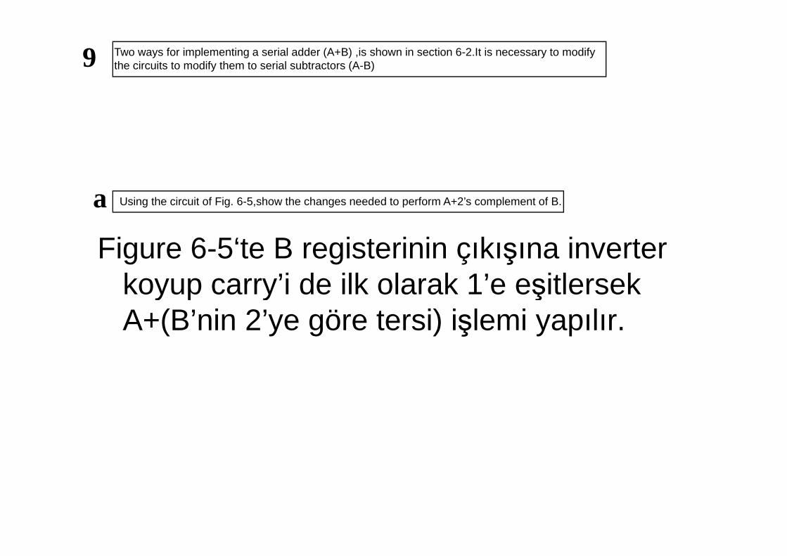
9 Two ways for implementing a serial adder (A+B) ,is shown in section 6-2.It is necessary to modify the circuits to modify them to serial subtractors (A-B)
a Using the circuit of Fig. 6-5,show the changes needed to perform A+2’s complement of B.
Figure 6-5‘te B registerinin çıkışına inverter koyup carry’i de ilk olarak 1’e eşitlersek koyup carry’i de ilk olarak 1’e eşitlersek A+(B’nin 2’ye göre tersi) işlemi yapılır.
Present Inputs Next Output FlipFlop
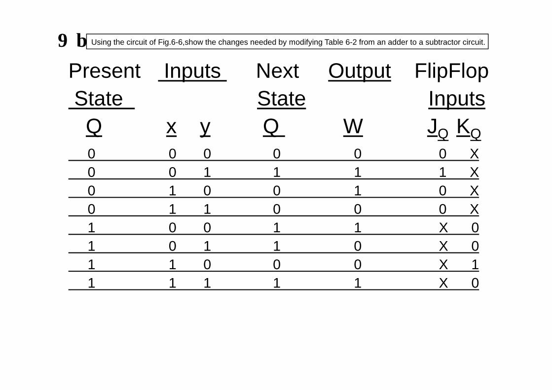
9 b Using the circuit of Fig.6-6,show the changes needed by modifying Table 6-2 from an adder to a subtractor circuit.
Present Inputs Next Output FlipFlop State State InputsState State InputsQ x y Q W JQ KQ0 0 0 0 0 0 X0 0 0 0 0 0 X0 0 1 1 1 1 X0 1 0 0 1 0 X 0 1 0 0 1 0 X 0 1 1 0 0 0 X1 0 0 1 1 X 0 1 0 1 1 0 X 01 0 1 1 0 X 01 1 0 0 0 X 11 1 1 1 1 X 0 1 1 1 1 1 X 0
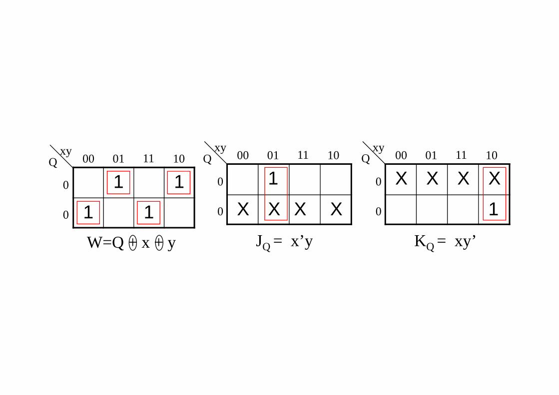
00 01 11 10xy 00 01 11 10
xy00 01 11 10
xyQ Q00 01 11 10
0
xyQ
100 01 11 10
0
xy
X X X X00 01 11 10
0
xyQ Q
1 1
0 X X X X0 10
W=Q + x + y JQ = x’y KQ = xy’
1 1
W=Q + x + y JQ = x’y KQ = xy’
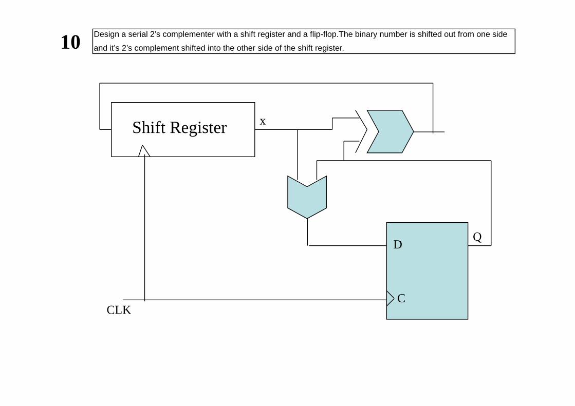
10Design a serial 2’s complementer with a shift register and a flip-flop.The binary number is shifted out from one side
and it’s 2’s complement shifted into the other side of the shift register.
Shift Register x
DQ
C
D
CCLK

11 A binary ripple counter uses flip-flops that trigger on the positive edge of the clock.What will be the count if; a)the normal outputs of the flip-flops are connected to the clock and b)the complement outputs of the flip-flops are connected to the clock?
a)Geriye doğru sayan sayıcı olur.a)Geriye doğru sayan sayıcı olur.
b)İleriye doğru sayan sayıcı olur.

12a AT
Draw the logic diagram of a 4-bit binary ripple down counter using a)flip-flops that trigger on the positive-edge of the clock and b) flip-flops that trigger on the negative-edge of the clock.
a A0T
CountC
A1T
Count
C
A2T
C
A3T
C
T
C
Lojik 1 Reset
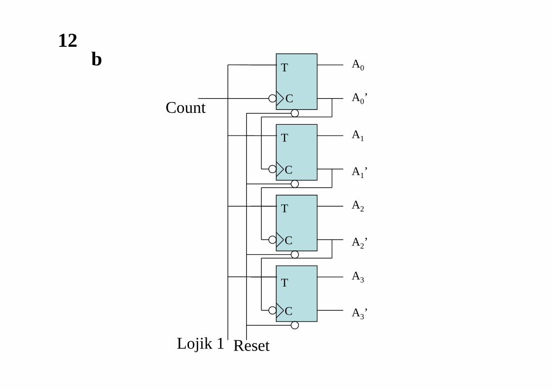
AT
12b A0T
CountC A0’
b
A1T
Count
C A1’
A2T
C A ’
A3T
C A2’
T
C A3’
Lojik 1 Reset
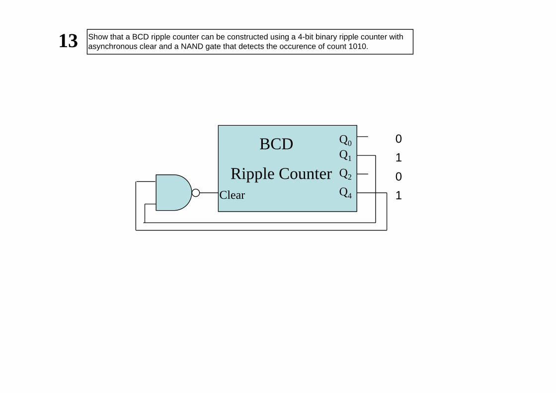
13 Show that a BCD ripple counter can be constructed using a 4-bit binary ripple counter with asynchronous clear and a NAND gate that detects the occurence of count 1010.
BCD Q0
Q 1
0BCD
Ripple CounterClear
Q1
Q2
Q4 1
1
0
Clear Q4 1
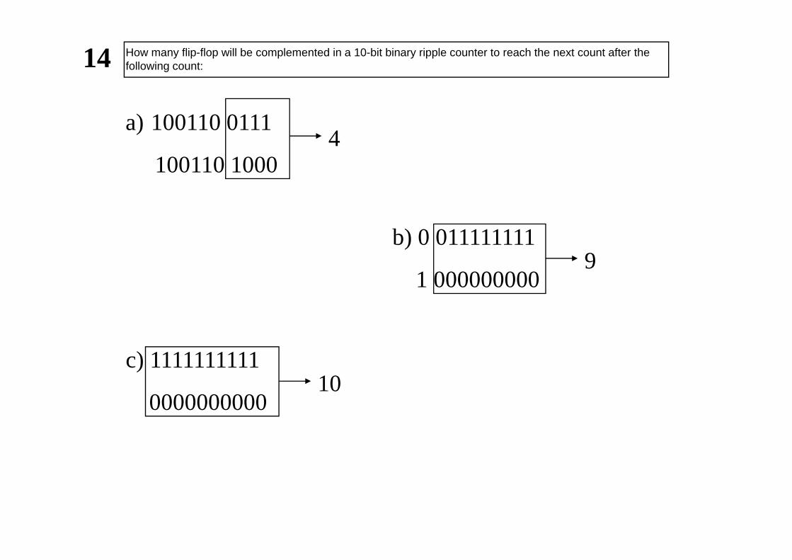
14 How many flip-flop will be complemented in a 10-bit binary ripple counter to reach the next count after the following count:
a) 100110 0111
100110 1000 4
100110 1000
b) 0 011111111
1 0000000009
1 000000000
c) 1111111111
000000000010
0000000000

15 A flip-flops has a 5 ns delay from the time the clock edge occurs to the time the output is complemented.What is the maximum delay in a 10-bit binary ripple counter that uses these flip-flops?What is the maximum
frequency the counter can operate reliably?frequency the counter can operate reliably?
Bütün flip-flop’ların complement olacağı düşünürlürse;
10 x 5 = 50 ns maksimum gecikme olacaktır.
Maksimum frequency ise
109/50 = 20 Mhz olur.

16 The BCD ripple counter shown in Fig. 6-10 has four flip-flops and 16 states ,of which only 10 are used.Analyze the circuit and determine the next state for each of the other unused states.What will happen if a noise signal sends the circuit to one of the unused states?
1010 1011 0100 1010 1011 0100
1011 0100
1100 1101 0100
1101 01001101 0100
1110 1111 0000
1111 0000
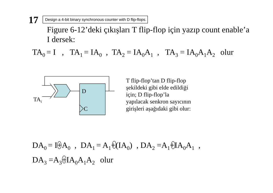
17Figure 6-12’deki çıkışları T flip-flop için yazıp count enable’a
Design a 4-bit binary synchronous counter with D flip-flops.
Figure 6-12’deki çıkışları T flip-flop için yazıp count enable’a I dersek:
TA0 = I , TA1 = IA0 , TA2 = IA0A1 , TA3 = IA0A1A2 olurTA0 = I , TA1 = IA0 , TA2 = IA0A1 , TA3 = IA0A1A2 olur
TA
D
T flip-flop’tan D flip-flop şekildeki gibi elde edildiği için; D flip-flop’la
TA i
C
için; D flip-flop’la yapılacak senkron sayıcının girişleri aşağıdaki gibi olur:
DA0 = I+A0 , DA1 = A1+(IA0) , DA2 =A1+IA0A1 ,
DA3 =A3+IA0A1A2 olurDA3 =A3+IA0A1A2 olur
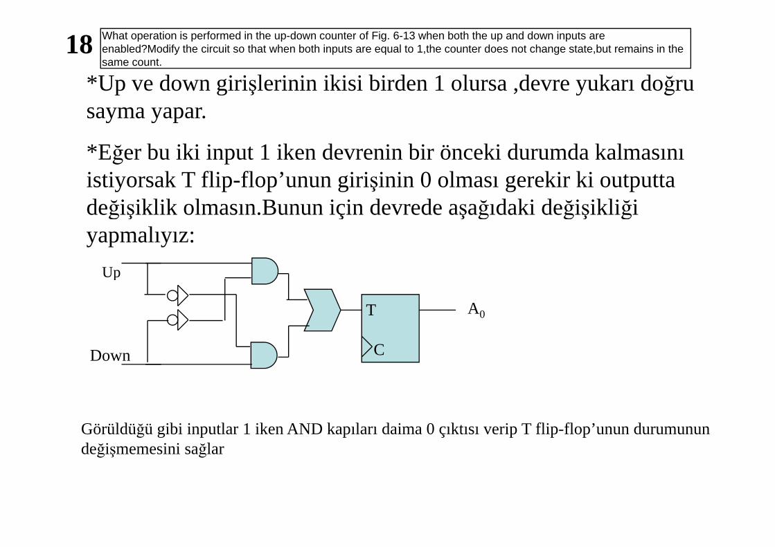
*Up ve down girişlerinin ikisi birden 1 olursa ,devre yukarı doğru
18 What operation is performed in the up-down counter of Fig. 6-13 when both the up and down inputs are enabled?Modify the circuit so that when both inputs are equal to 1,the counter does not change state,but remains in the same count.
*Up ve down girişlerinin ikisi birden 1 olursa ,devre yukarı doğru sayma yapar.
*Eğer bu iki input 1 iken devrenin bir önceki durumda kalmasını *Eğer bu iki input 1 iken devrenin bir önceki durumda kalmasını istiyorsak T flip-flop’unun girişinin 0 olması gerekir ki outputta değişiklik olmasın.Bunun için devrede aşağıdaki değişikli ği değişiklik olmasın.Bunun için devrede aşağıdaki değişikli ği yapmalıyız:
Up
A0T
Up
CDown
Görüldüğü gibi inputlar 1 iken AND kapıları daima 0 çıktısı verip T flip-flop’unun durumunun değişmemesini sağlar
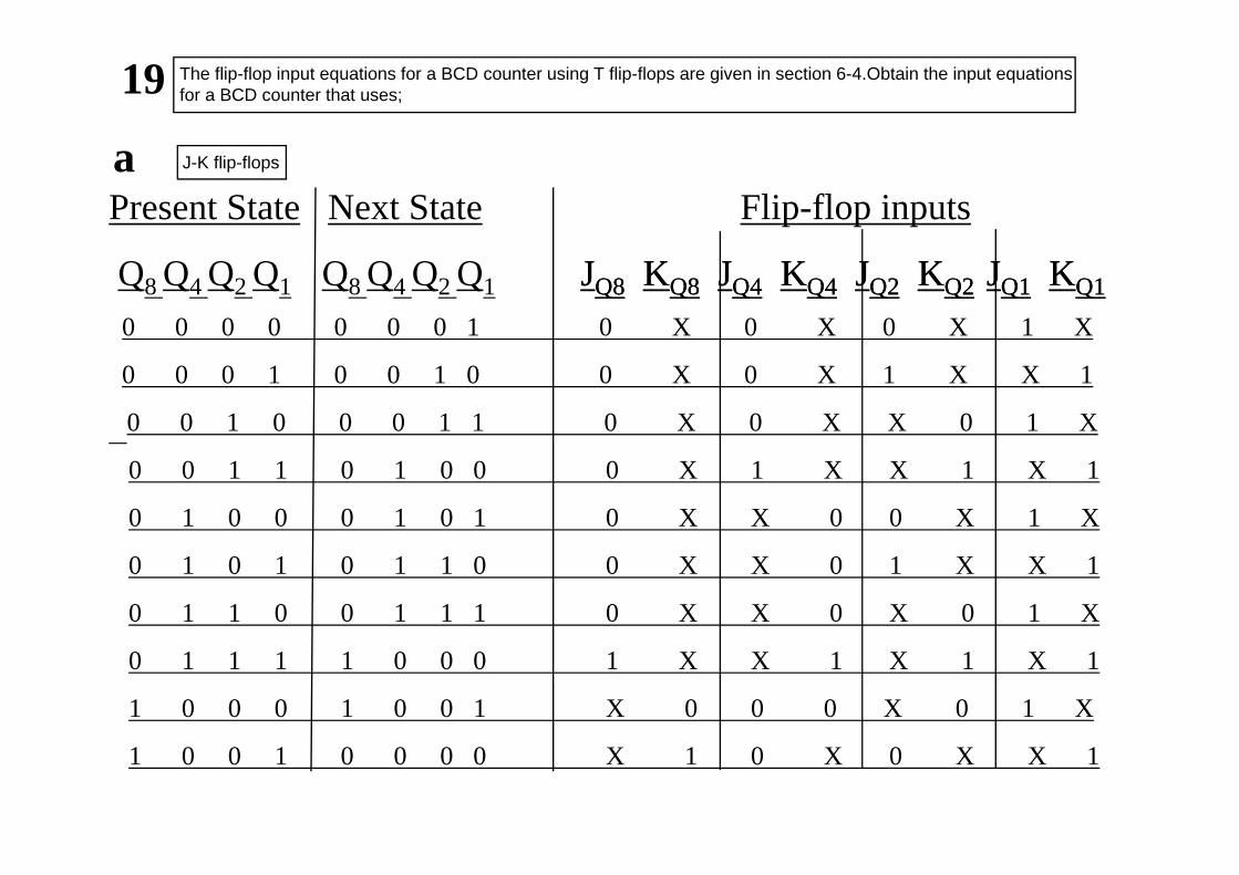
19
a
The flip-flop input equations for a BCD counter using T flip-flops are given in section 6-4.Obtain the input equations for a BCD counter that uses;
aPresent StateNext State Flip-flop inputs
J-K flip-flops
Q8 Q4 Q2 Q1 Q8 Q4 Q2 Q1 JJQQ88 KKQQ88 JJQQ44 KKQQ44 JJQQ22 KKQQ22 JJQQ11 KKQQ11
0 0 0 0 0 0 0 1 0 X 0 X 0 X 1 X0 0 0 0 0 0 0 1 0 X 0 X 0 X 1 X
0 0 0 1 0 0 1 0 0 X 0 X 1 X X 1
0 0 1 0 0 0 1 1 0 X 0 X X 0 1 X
0 0 1 1 0 1 0 0 0 X 1 X X 1 X 1
0 1 0 0 0 1 0 1 0 X X 0 0 X 1 X
0 1 0 1 0 1 1 0 0 X X 0 1 X X 1
0 1 1 0 0 1 1 1 0 X X 0 X 0 1 X
0 1 1 1 1 0 0 0 1 X X 1 X 1 X 1
1 0 0 0 1 0 0 1 X 0 0 0 X 0 1 X
1 0 0 1 0 0 0 0 X 1 0 X 0 X X 1
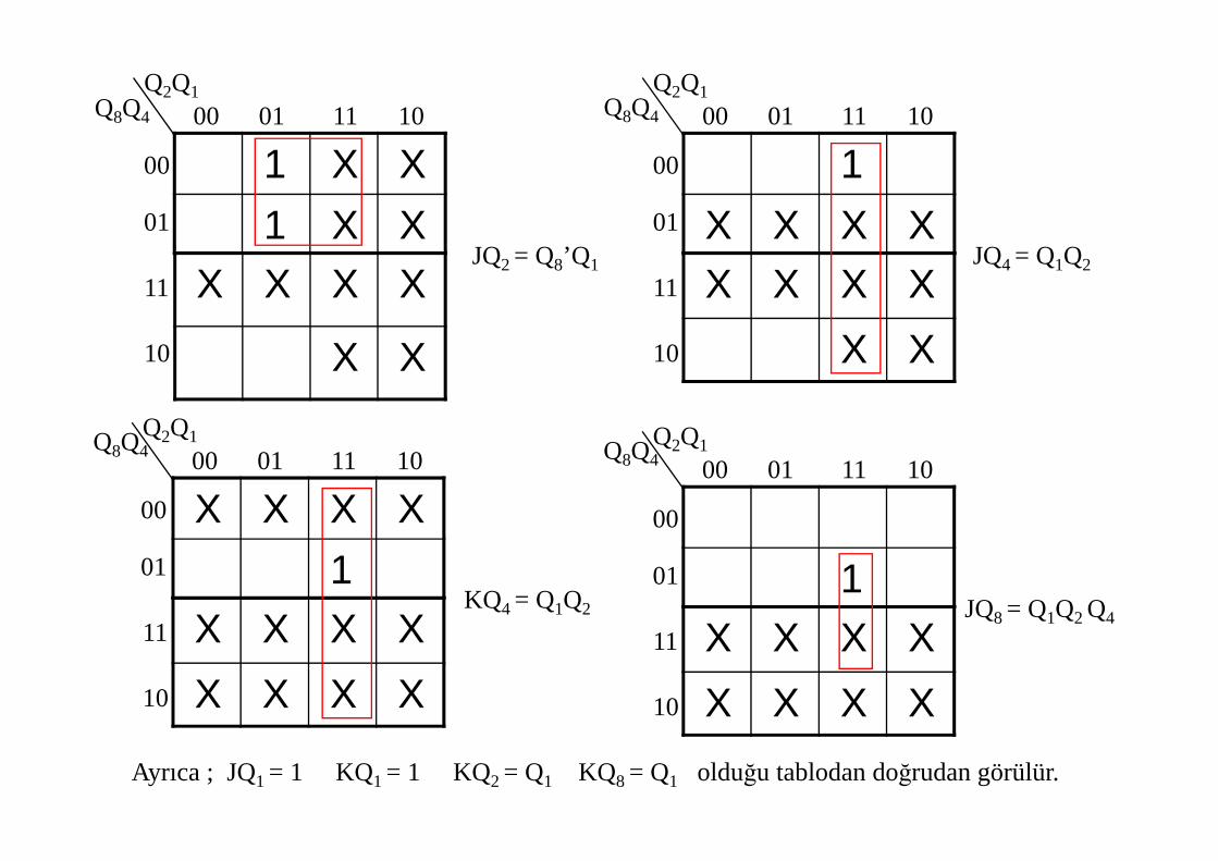
00 01 11 10Q8Q4
Q2Q1
00 01 11 10Q2Q1
Q8Q4
1 X X
1 X X
00
01
1
X X X X
00
011 X X
X X X X
01
11
X X X X
X X X X
X X
01
11JQ2 = Q8’Q1 JQ4 = Q1Q2
X X10 X X10
Q2Q1Q Q Q Q
X X X X 00 01 11 10
00
Q2Q1Q8Q400 01 11 10
00
Q2Q1Q8Q4
X X X X
1
X X X X
01
11
1
X X X X
00
01KQ4 = Q1Q2 JQ8 = Q1Q2 Q4 X X X X
X X X X
11
10
X X X X
X X X X
11
10 X X X X
Ayrıca ; JQ1 = 1 KQ1 = 1 KQ2 = Q1 KQ8 = Q1 olduğu tablodan doğrudan görülür.
Present StateNext StateQ8 Q4 Q2 Q1 Q8 Q4 Q2 Q10 0 0 0 0 0 0 1
00 01 11 10Q2Q1
Q8Q4
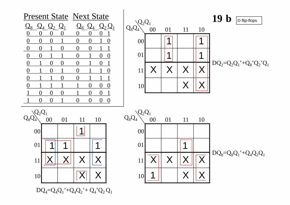
19 b D flip-flops
0 0 0 0 0 0 0 10 0 0 1 0 0 1 00 0 1 0 0 0 1 10 0 1 1 0 1 0 0
1 1
1 1
00 01 11 10
00
010 0 1 1 0 1 0 00 1 0 0 0 1 0 10 1 0 1 0 1 1 00 1 1 0 0 1 1 1
1 1
X X X X
01
11DQ2=Q2Q1’+Q8’Q2’Q1
0 1 1 0 0 1 1 10 1 1 1 1 0 0 01 0 0 0 1 0 0 11 0 0 1 0 0 0 0
X X10
1 0 0 1 0 0 0 0
100 01 11 10
Q2Q1Q8Q4 00 01 11 10
Q2Q1Q8Q4
1
1 1 1
00
01 1
00
011 1 1
X X X X
X X
11
1
X X X X
1 X X
11DQ8=Q8Q1’+Q4Q2Q1
X X10
DQ4=Q4Q1’+Q4Q2’+ Q4’Q2 Q1
1 X X10

20a)
AAAA
Enclose the binary counter with paraller load of Fig. 6-14 in a block diagram showing all inputs and outputs.
Show the connections of four such blocks to produce a 16-bit counter with parallel load.
Load
A0A1A2A3
Carry
Clear
Count
Clear
CLK
Carry
16 bitlik sayıcı oluşturmak için her bir devrenin carry çıkışını bir sonrakinin Count girişine bağlamalıyız.Bu işlem ClearClear
I3 I2 I1 I0
Count girişine bağlamalıyız.Bu işlem için bu devreden 4 tane gereklidir.
I3 I2 I1 I0
b) Construct a binary counter that counts from 0 to 64.
4-Bit counterCLKCLRLoad 4-Bit counter
CLKCLRCarry4-Bit counter CLR
Count
0
Carry
4-Bit counter CLR
Count
0
Load
0 0

21 The counter of Fig. 6-14 has two control inputs Load(L) and Count(C) and a data input ,(Ii).
a)JA0 = CL’ + I0L
Derive the flip-flop input equations for J and K of the first stage in terms of L,C,and I.
0 0
KA0 = LI0’ + L’C
b)J = [L(LI’)][L + C] = (L’ + LI)(L + C)=L’C + LI
The logic diagram of the first stage of an equivalent integrated circuit is shown in Fig. P6-21.Verift that this circuit is equivalent to the one in a.
J = [L(LI’)][L + C] = (L’ + LI)(L + C)=L’C + LI
K = (LI’)(L + C) = (L’ + I’)(L + C) = L’C + LI’K = (LI’)(L + C) = (L’ + I’)(L + C) = L’C + LI’

22A0A1A2A3
Using the circuit of Fig. 6-14, design a mod-12 counter:
Clear
A0A1A2A3
1011(11) olduktan sonraki clock darbesi ile inputlar
Load Count
Clear
CLK
clock darbesi ile inputlar sayaca yüklenir ve sayaç sıfırlanır.Load Count
0
Using an AND gate and the load input
0
A0A1A2A3
Load 1100(12) olduğu anda sayaç sıfırlanır.
Count
CLK
Clear
sayaç sıfırlanır.
Using an NAND gate and the asynchronous clear input
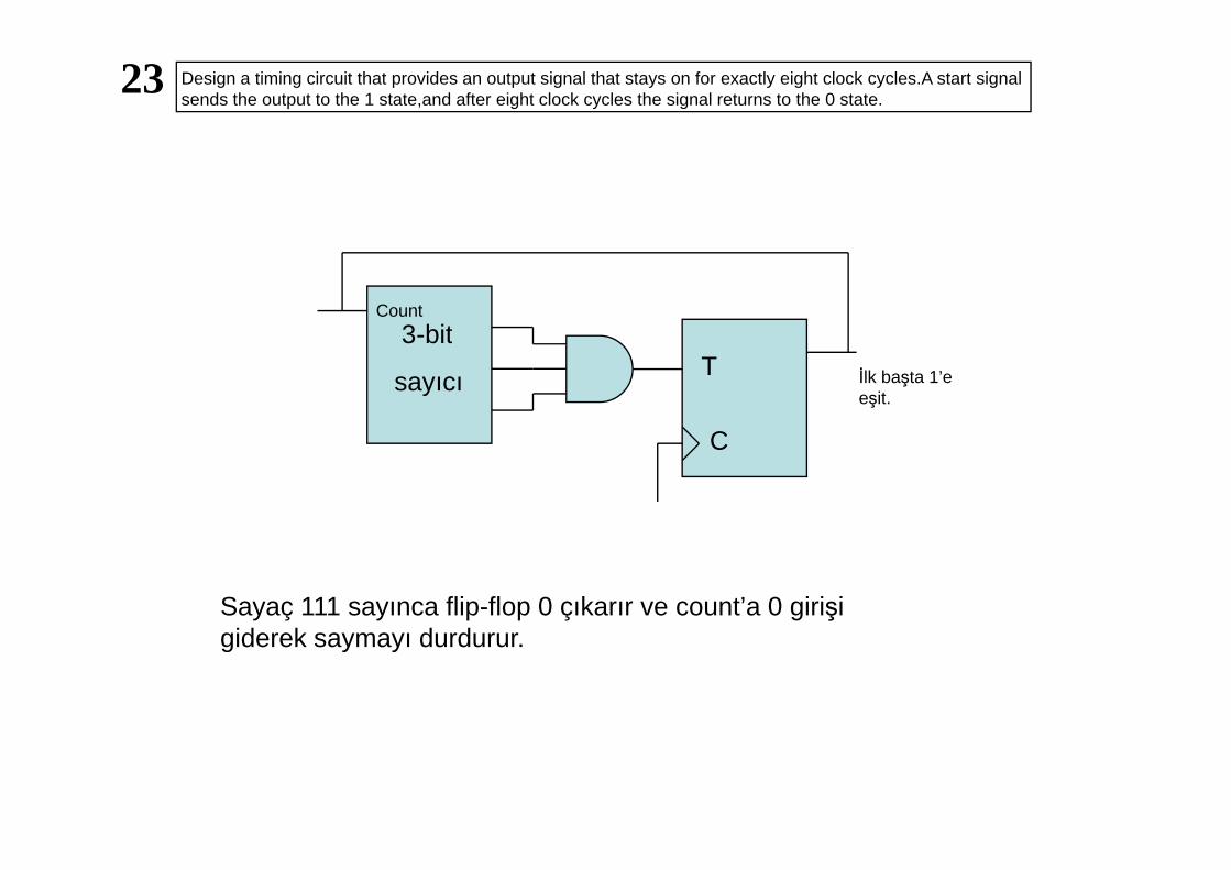
23 Design a timing circuit that provides an output signal that stays on for exactly eight clock cycles.A start signal sends the output to the 1 state,and after eight clock cycles the signal returns to the 0 state.
3-bitCount
3-bit
sayıcıT
C
İlk başta 1’e eşit.
C
Sayaç 111 sayınca flip-flop 0 çıkarır ve count’a 0 girişi giderek saymayı durdurur.giderek saymayı durdurur.

24Present State Next State Flip-flop inputs
Design a counter with T flip-flops that goes through the following binary repeated sequence: 0,1,3,7,6,4.Show that when binary states 010 and 101 are considered as don’t care conditions,the counter may operate properly.Find a correct way to design.
A B C A B C TA TB TC
0 0 0 0 0 1 0 0 10 0 0 0 0 1 0 0 1
0 0 1 0 1 1 0 1 0
0 1 0 X X X X X X0 1 0 X X X X X X
0 1 1 1 1 1 1 0 0
1 0 0 0 0 0 1 0 0
1 0 1 X X X X X X
1 1 0 1 0 0 0 1 0
1 1 1 1 1 0 0 0 1
00 01 11 10BC
A 00 01 11BC
A 10 00 01 11 10BC
A
1 X
1 X
0
0
1 X
1 X
0
0
1 X
X 1
0
01 X0
TA =A + B
1 X0
TB = B + C
X 1 0
TC = A + C
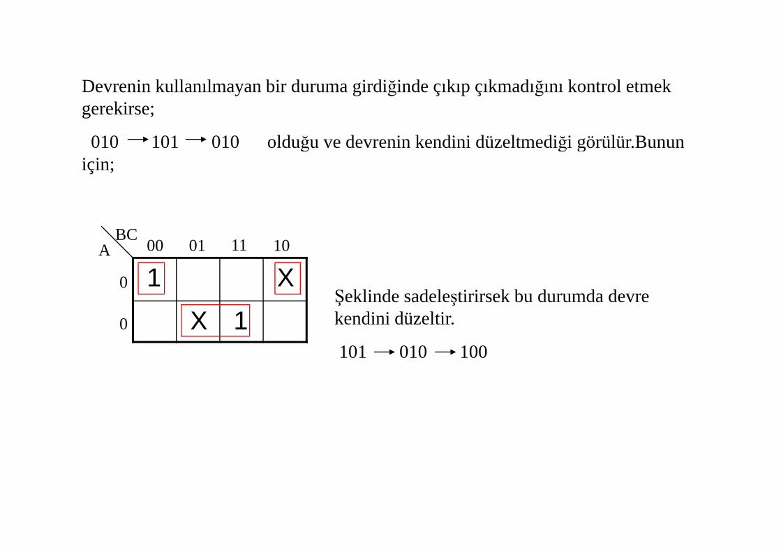
Devrenin kullanılmayan bir duruma girdiğinde çıkıp çıkmadığını kontrol etmek Devrenin kullanılmayan bir duruma girdiğinde çıkıp çıkmadığını kontrol etmek gerekirse;
010 101 010 olduğu ve devrenin kendini düzeltmediği görülür.Bunun 010 101 010 olduğu ve devrenin kendini düzeltmediği görülür.Bunun için;
1 X 00 01 11 10
0
BCA
1 X
X 1
0
0
Şeklinde sadeleştirirsek bu durumda devre kendini düzeltir.
101 010 100

25
a
It is necessary to generate six repeated timing signals T0 through T5 similar to the ones shown in Fig. 6-17(c).Design the timing circuit using:
a)Flip-flops only b)A counter and a decoder.
a
T T T T T TT0 T1 T2 T3 T4 T5
Sağa kaydır
Tb3-Bit Counter 3 X 8 Counter
T0
T1T2T
0124
3-Bit Counter 3 X 8 CounterT3
T4
T5
456

26 A digital system has a clock generator that produces pulses at a frequency of 80 Mhz.Design a circuit that provides a clock with a cycle time of 50 ns.
(1000 x 10-9) / 50 = 20Mhz olur.
Bu durumda 80 ‘i 4’te birine indirmek için bir 2-bit sayıcı kullanmamız gerekir.gerekir.

27 Present State Next State Flip-flop inputs
A B C A B C J K J K J KA B C A B C JA KA JB KB JC KC
0 0 0 0 0 1 0 X 0 X 1 X
0 0 1 0 1 0 0 X 1 X X 1 Design a counter with 0 0 1 0 1 0 0 X 1 X X 1
0 1 0 0 1 1 0 X X 0 1 X
0 1 1 1 0 0 1 X X 1 X 1
Design a counter with the following repeated binary sequence:0,1,3,4,5,6.Use JK flip-flops.
0 1 1 1 0 0 1 X X 1 X 1
1 0 0 1 0 1 X 0 0 X 1 X
1 0 1 1 1 0 X 0 1 X X 1
Use JK flip-flops.
1 0 1 1 1 0 X 0 1 X X 1
1 1 0 0 0 0 X 1 X 1 0 X
1 1 1 X X X X X X X X X 1 1 1 X X X X X X X X X
100 01 11 10
BCA
X X 100 01 11 10
BCA
1 X X 1 00 01 11 10
BCA
1
X X X X
0
0
X X 1
X X X 1
0
0
1 X X 1
1 X X
0
0
JA = BC KA = B
X X X 1
KB = A + C JB = C
1 X X 0
JC = A’ + B’ KC = 1
28 Present State Next State
A B C A B C 00 01 11 10
BCA
A B C A B C 0 0 0 0 0 1
0 0 1 0 1 0
X 1
1 X X
0
0DA = A+B
0 0 1 0 1 0
0 1 0 1 0 0
0 1 1 X X X
1 X X 0
00 01 11 10BC
A
Design a counter with the following
0 1 1 X X X
1 0 0 1 1 0
1 0 1 X X X
1 X
1 X X
00 01 11 10
0
A
DB = AB’+C
following repeated binary sequence:0,1,2,4,6.Use D flip-flops.
1 0 1 X X X
1 1 0 0 0 0
1 1 1 X X X
1 X X 0
1 1 1 X X X
1 X00 01 11 10
0
BCA
011 110 101 110 111 010 1 X
X X
0
0DC = A’B’C’
011 110 101 110 111 010
Görüldüğü üzere devre beklenmeyen
duruma girdiği zaman kendini düzeltirduruma girdiği zaman kendini düzeltir
29
Present StateNext State
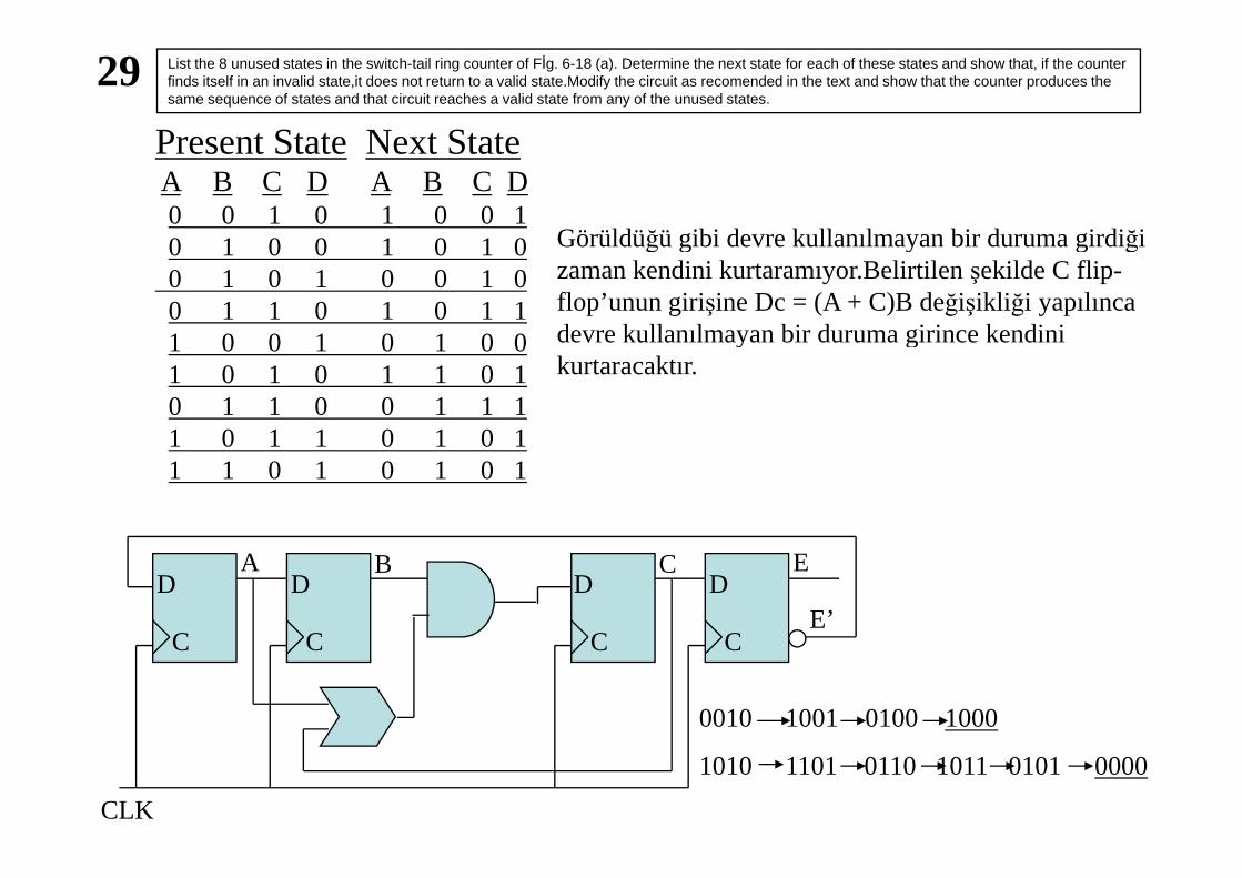
List the 8 unused states in the switch-tail ring counter of Fİg. 6-18 (a). Determine the next state for each of these states and show that, if the counter finds itself in an invalid state,it does not return to a valid state.Modify the circuit as recomended in the text and show that the counter produces the same sequence of states and that circuit reaches a valid state from any of the unused states.
Present StateNext StateA B C D A B C D0 0 1 0 1 0 0 10 1 0 0 1 0 1 0Görüldüğü gibi devre kullanılmayan bir duruma girdiği 0 1 0 0 1 0 1 00 1 0 1 0 0 1 00 1 1 0 1 0 1 11 0 0 1 0 1 0 0
Görüldüğü gibi devre kullanılmayan bir duruma girdiği zaman kendini kurtaramıyor.Belirtilen şekilde C flip-flop’unun girişine Dc = (A + C)B değişikli ği yapılınca devre kullanılmayan bir duruma girince kendini 1 0 0 1 0 1 0 0
1 0 1 0 1 1 0 10 1 1 0 0 1 1 11 0 1 1 0 1 0 1
devre kullanılmayan bir duruma girince kendini kurtaracaktır.
1 0 1 1 0 1 0 11 1 0 1 0 1 0 1
D
C
D
C
D
C
D
C
A B C E
E’C C C C
0010 1001 0100 1000
CLK
1010 1101 0110 1011 0101 0000
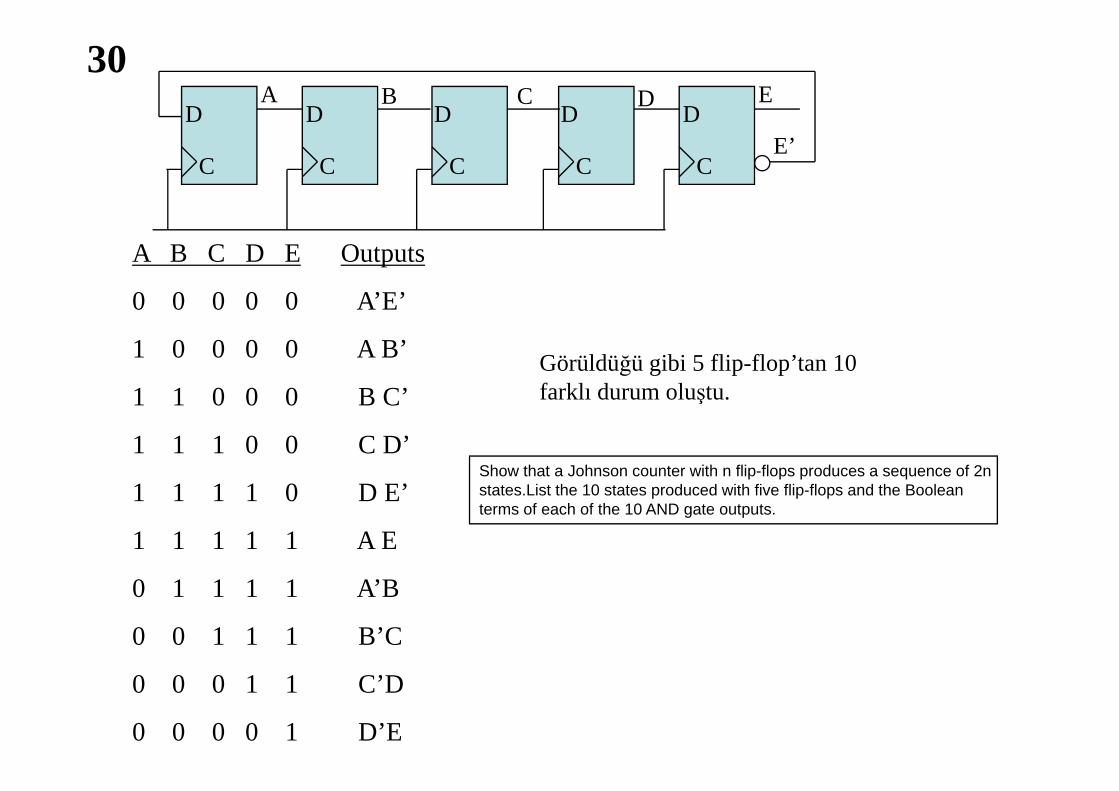
30D D D D
A B C ED
DD
C
D
C
D
C
D
CE’
D
C
A B C D E Outputs
0 0 0 0 0 A’E’0 0 0 0 0 A’E’
1 0 0 0 0 A B’
1 1 0 0 0 B C’Görüldüğü gibi 5 flip-flop’tan 10 farklı durum oluştu.1 1 0 0 0 B C’
1 1 1 0 0 C D’
1 1 1 1 0 D E’
farklı durum oluştu.
Show that a Johnson counter with n flip-flops produces a sequence of 2n states.List the 10 states produced with five flip-flops and the Boolean 1 1 1 1 0 D E’
1 1 1 1 1 A E
0 1 1 1 1 A’B
states.List the 10 states produced with five flip-flops and the Boolean terms of each of the 10 AND gate outputs.
0 1 1 1 1 A’B
0 0 1 1 1 B’C
0 0 0 1 1 C’D
0 0 0 0 1 D’E