October, 2001 CMS Tracker Electronics 1
Module studies at IC
OUTLINE
laboratory setup description, APV I2C settingspulse shape studies (dependence on ISHA, VFS)results with β source (effect of varying det. bias)noise performance (PA resistance contribution)on-chip CM subtraction explanation for unbonded channel behaviourconclusions
emphasis on verifying APV performance and understanding any unexpected behaviourDCU not studied (yet)
Mark Raymond([email protected])
October, 2001 CMS Tracker Electronics 2
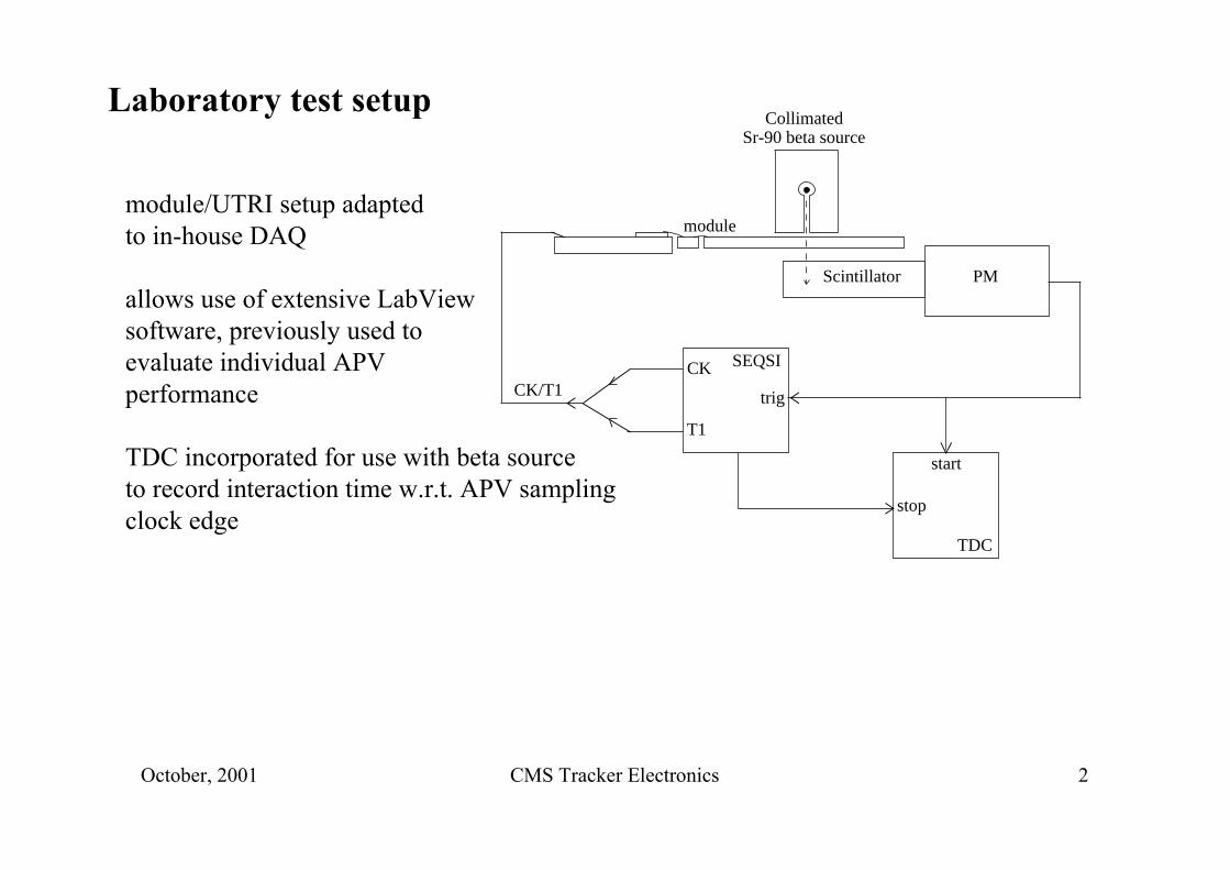
Laboratory test setup
Scintillator
CollimatedSr-90 beta source
PM
start
stop
TDC
SEQSI
trig
T1
CK/T1CK
modulemodule/UTRI setup adaptedto in-house DAQ
allows use of extensive LabViewsoftware, previously used toevaluate individual APVperformance
TDC incorporated for use with beta sourceto record interaction time w.r.t. APV samplingclock edge
October, 2001 CMS Tracker Electronics 3
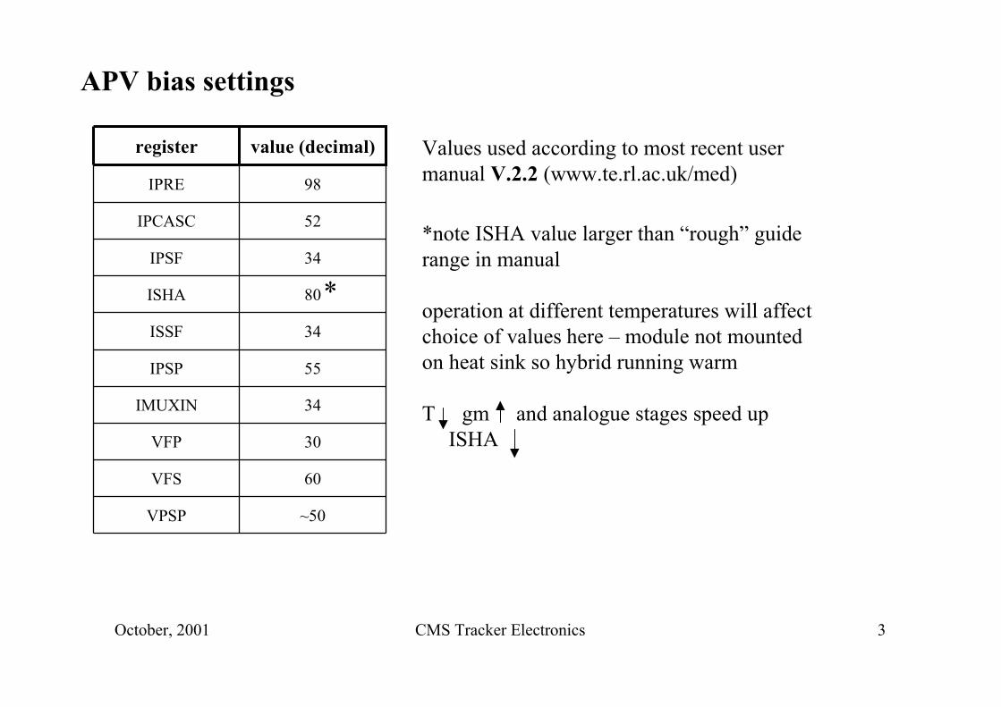
APV bias settings
~50VPSP
60VFS
30VFP
34IMUXIN
55IPSP
34ISSF
80ISHA
34IPSF
52IPCASC
98IPRE
value (decimal)register
*
Values used according to most recent user manual V.2.2 (www.te.rl.ac.uk/med)
*note ISHA value larger than “rough” guide range in manual
operation at different temperatures will affectchoice of values here – module not mountedon heat sink so hybrid running warm
T gm and analogue stages speed upISHA
October, 2001 CMS Tracker Electronics 4
120
100
80
60
40
20
0
AD
C u
nits
VFS=0
VFS=120
ideal CR-RC ISHA=80,VFS=60
100
80
60
40
20
0
-20
AD
C u
nits
100806040200
3.125 ns steps
VFS=0
VFS=120
ISHA=80,VFS=60
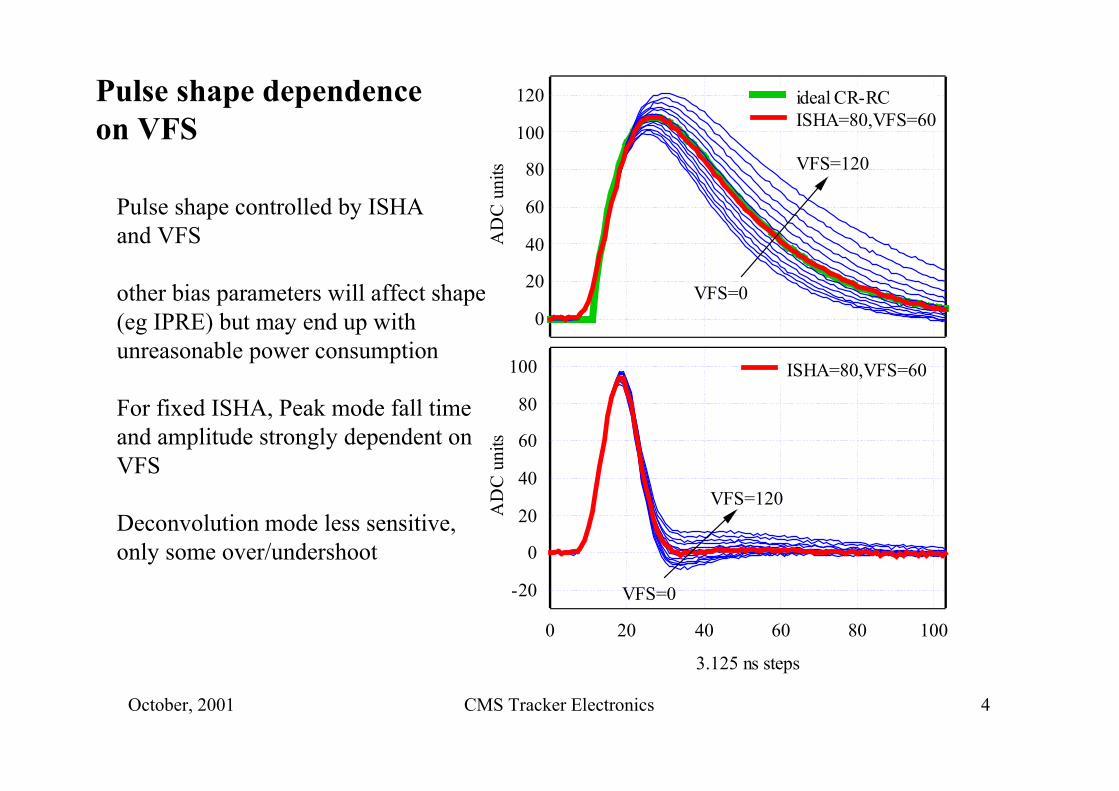
Pulse shape dependence on VFS
Pulse shape controlled by ISHA and VFS
other bias parameters will affect shape(eg IPRE) but may end up with unreasonable power consumption
For fixed ISHA, Peak mode fall time and amplitude strongly dependent on VFS
Deconvolution mode less sensitive, only some over/undershoot
October, 2001 CMS Tracker Electronics 5
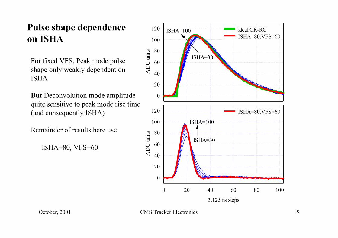
Pulse shape dependence on ISHA
For fixed VFS, Peak mode pulse shape only weakly dependent on ISHA
But Deconvolution mode amplitude quite sensitive to peak mode rise time (and consequently ISHA)
Remainder of results here use
ISHA=80, VFS=60
120
100
80
60
40
20
0
AD
C u
nits
ISHA=30
ISHA=100 ideal CR-RC ISHA=80,VFS=60
120
100
80
60
40
20
0
AD
C u
nits
100806040200
3.125 ns steps
ISHA=30
ISHA=100
ISHA=80,VFS=60
October, 2001 CMS Tracker Electronics 6
200
150
100
50
0
AD
C c
ount
s
1009080706050403020100
TDC steps [ns]
50 ns50 ns
HT=100 V200
150
100
50
0
AD
C c
ount
s
1009080706050403020100
TDC steps [ns]
50 ns50 ns
HT=250 V
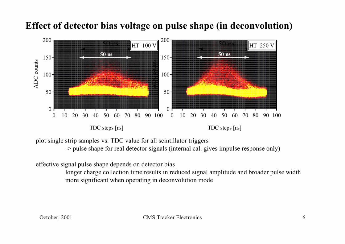
Effect of detector bias voltage on pulse shape (in deconvolution)
plot single strip samples vs. TDC value for all scintillator triggers-> pulse shape for real detector signals (internal cal. gives impulse response only)
effective signal pulse shape depends on detector biaslonger charge collection time results in reduced signal amplitude and broader pulse widthmore significant when operating in deconvolution mode
October, 2001 CMS Tracker Electronics 7
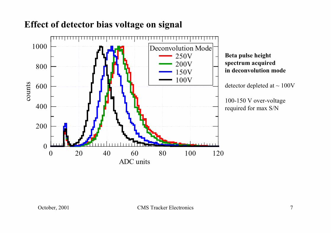
Effect of detector bias voltage on signal
Beta pulse height spectrum acquired in deconvolution mode
detector depleted at ~ 100V
100-150 V over-voltagerequired for max S/N
1000
800
600
400
200
0
coun
ts
120100806040200ADC units
Deconvolution Mode 250V 200V 150V 100V
October, 2001 CMS Tracker Electronics 8
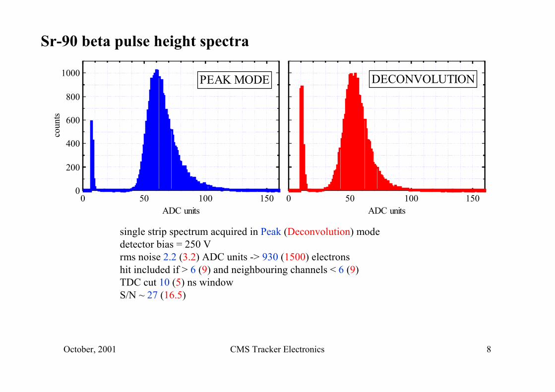
Sr-90 beta pulse height spectra
single strip spectrum acquired in Peak (Deconvolution) modedetector bias = 250 Vrms noise 2.2 (3.2) ADC units -> 930 (1500) electronshit included if > 6 (9) and neighbouring channels < 6 (9)TDC cut 10 (5) ns windowS/N ~ 27 (16.5)
1000
800
600
400
200
0
coun
ts
150100500ADC units
PEAK MODE
150100500ADC units
DECONVOLUTION
October, 2001 CMS Tracker Electronics 9
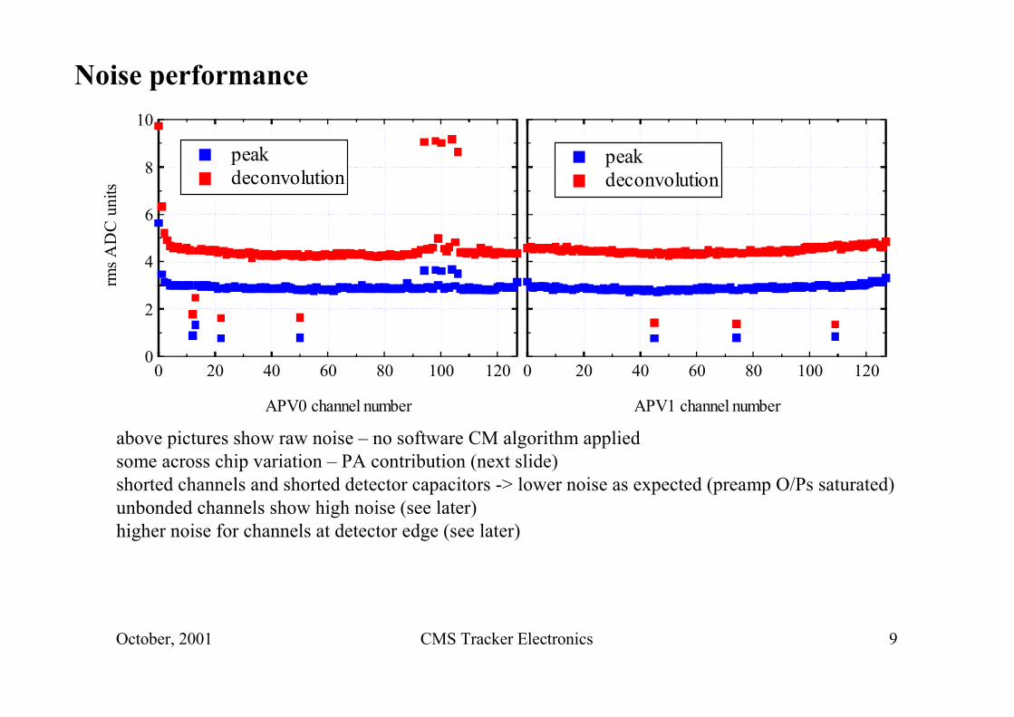
Noise performance10
8
6
4
2
0
rms A
DC
uni
ts
120100806040200
APV0 channel number
peak deconvolution
120100806040200
APV1 channel number
peak deconvolution
above pictures show raw noise – no software CM algorithm appliedsome across chip variation – PA contribution (next slide)shorted channels and shorted detector capacitors -> lower noise as expected (preamp O/Ps saturated)unbonded channels show high noise (see later)higher noise for channels at detector edge (see later)
October, 2001 CMS Tracker Electronics 10
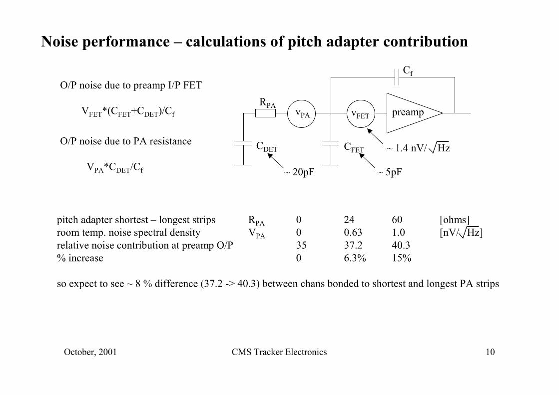
Noise performance – calculations of pitch adapter contribution
pitch adapter shortest – longest strips RPA 0 24 60 [ohms]room temp. noise spectral density VPA 0 0.63 1.0 [nV/ Hz]relative noise contribution at preamp O/P 35 37.2 40.3% increase 0 6.3% 15%
so expect to see ~ 8 % difference (37.2 -> 40.3) between chans bonded to shortest and longest PA strips
vFETvPA
CFET
preamp
CDET
RPA
~ 1.4 nV/ Hz
~ 5pF~ 20pF
Cf
O/P noise due to preamp I/P FET
VFET*(CFET+CDET)/Cf
O/P noise due to PA resistance
VPA*CDET/Cf
October, 2001 CMS Tracker Electronics 11
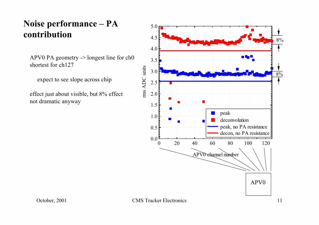
5.0
4.5
4.0
3.5
3.0
2.5
2.0
1.5
1.0
0.5
0.0rm
s AD
C u
nits
120100806040200
APV0 channel number
8%
8%
peak deconvolution peak, no PA resistance decon, no PA resistance
APV0
Noise performance – PAcontribution
APV0 PA geometry -> longest line for ch0shortest for ch127
expect to see slope across chip
effect just about visible, but 8% effectnot dramatic anyway
October, 2001 CMS Tracker Electronics 12
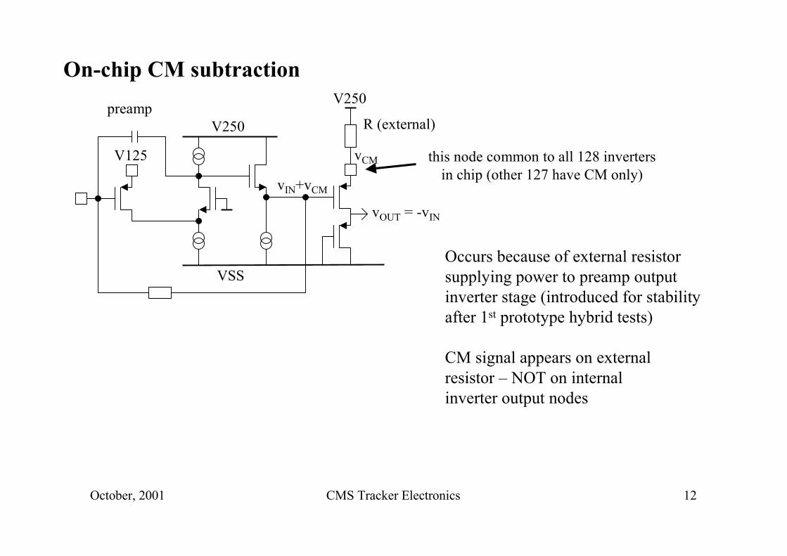
On-chip CM subtraction
Occurs because of external resistor supplying power to preamp output inverter stage (introduced for stabilityafter 1st prototype hybrid tests)
CM signal appears on externalresistor – NOT on internalinverter output nodes
V125
V250
VSS
V250
R (external)
vIN+vCM
vCM
vOUT = -vIN
this node common to all 128 invertersin chip (other 127 have CM only)
preamp
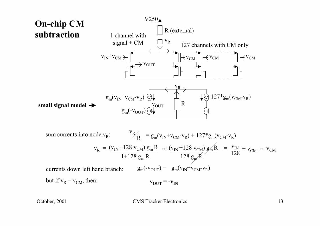
October, 2001 CMS Tracker Electronics 13
On-chip CMsubtraction
vIN+vCM vCM
1 channel withsignal + CM 127 channels with CM only
R (external)
V250
vR
small signal model Rgm(vIN+vCM-vR)
gm(-vOUT)
127*gm(vCM-vR)
vCM vCM
vR
vOUT
vOUT
vRR = gm(vIN+vCM-vR) + 127*gm(vCM-vR)
(vIN +128 vCM) gm R1+128 gm R
vR = ≈ (vIN +128 vCM) gm R128 gm R
= vIN128
+ vCM ≈ vCM
sum currents into node vR:
currents down left hand branch: gm(vIN+vCM-vR)gm(-vOUT) =
but if vR = vCM, then: vOUT = -vIN
October, 2001 CMS Tracker Electronics 14
-100
0
10016
-100
0
10032
-100
0
10048
-100
0
10064
-100
0
10080
-100
0
10096
-100
0
100112
-100
0
100
100500
128
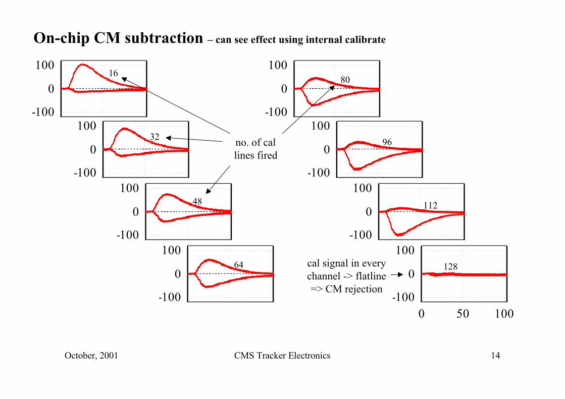
On-chip CM subtraction – can see effect using internal calibrate
no. of callines fired
cal signal in everychannel -> flatline=> CM rejection
October, 2001 CMS Tracker Electronics 15
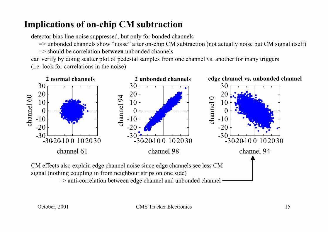
Implications of on-chip CM subtractiondetector bias line noise suppressed, but only for bonded channels
=> unbonded channels show “noise” after on-chip CM subtraction (not actually noise but CM signal itself)=> should be correlation between unbonded channels
can verify by doing scatter plot of pedestal samples from one channel vs. another for many triggers(i.e. look for correlations in the noise)
-30-20-10
0102030
chan
nel 9
4
-30-20-10 0 102030channel 98
-30-20-10
0102030
chan
nel 6
0
-30-20-10 0 102030channel 61
2 normal channels 2 unbonded channels
CM effects also explain edge channel noise since edge channels see less CM signal (nothing coupling in from neighbour strips on one side)
=> anti-correlation between edge channel and unbonded channel
-30-20-10
0102030
chan
nel 0
-30-20-10 0 102030channel 94
edge channel vs. unbonded channel
October, 2001 CMS Tracker Electronics 16
1.2
0.8
0.4
0.0
Vol
ts
1.2x10⁻⁶ 0.80.60.40.20.0-0.2-0.4
time
digital headeramplitude forAPVs 1 & 2
1.2x10⁻⁶ 0.80.60.40.20.0-0.2-0.4
time
dig. head.amp. APV3
dig. head.amp. APV4
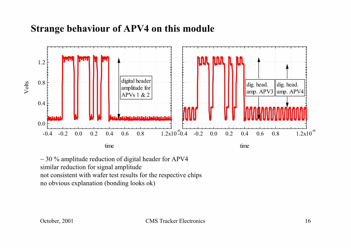
Strange behaviour of APV4 on this module
~ 30 % amplitude reduction of digital header for APV4similar reduction for signal amplitudenot consistent with wafer test results for the respective chipsno obvious explanation (bonding looks ok)
October, 2001 CMS Tracker Electronics 17
Conclusions
1st opportunity for us (at IC) to examine APV performance with full size CMS detectors
no nasty surprises, module performance (pulse shape, noise) appears good consistent with predictions from individual chip measurementsand consistent with detectors produced by others
unbonded channels behaviour understood in terms of on-chip CM subtractionnote: on-chip subtraction only takes care of CM occurring in or previous
to preamp


