ecal mother boards - istituto nazionale di fisica nuclearebatta/jlab/pratolongo_mb.pdf · noise...
TRANSCRIPT

1
Ecal Mother BoardsFabio Pratolongo
INFN-GEItaly

2
✴MB connect preamplifiers and HV from the ECal to crates
✴MB extend on Left/Right sides out the vessel to host signal and HV connectors
ECal Motherboard

3
✴Noise issues with many channels of the motherboards related to design (trace high density) and manufacturing (HV shorts for few channels and LV short for a whole MB)
✴ No time to debug and fix problems
✴ New simplified design, keeping the trace density and length as short as possible manufactured well in advance and fully tested
✴ Short vertical motherboards with connectors (power and signal) on top/bottom
✴ Design solutions taken from IC / FT-CAL experience (IPN-Orsay and INFN-Genova design)
ECal Motherboard

4
ECal Motherboard Mechanical design
✴ Mechanical design: IPN-Orsay
✴ Final design after iterations between Genova, Orsay and JLab
✴ Mechanics defined: 4 MB (TL, TR, BL, BR)

5
HPS Motherboard Electronic Design✴ Electrical design: INFN-GE Electronic Service
✴ Design coordinated with JLab (to reuse existing parts: cables, connectors ...)
✴ First step (ORCAD) finished
✴ Last step (ALEGRO) just started
PCB: 10 layers 3 signals + 1 HV + 1 fan-out + 5 GND
• 4 PCB (115, 115, 106, 106 channels each)• E.g.: TOP LEFT board (115 chs)
•115 SMD connectors (AMP 10 pin, same as used in FT-Cal) for preamps very similar to old MB (pin slightly smaller),
• 15 TE signal connectors from 16 pin each, same as old MB• 2 HV connectors (15 pin) DSUB 750V, 5A, different from old MB for easier routing. • 1 LV connectors (6 pin).
• Same HV grouping (as old MB) • Same 3M signal signal cable
Layout specifications:115 signal traces with 50 Ohms impedance.Signal: 0.2 mm line width and 0.2 mm min. spacing.HV: 0.6 mm line width and 0.9 mm min. spacing.Ground ring between two signals as FT-Cal project.

6
LEFT TOP Design (115 channels)

7
LEFT BOTTOM Design (115 channels)

8
HV Grouping
• Old: hits-load well distributed• New: simple trace routing • We are working to find a compromise
New (proposed)
OLD

9
LEFT TOP Routing (preliminary)
10
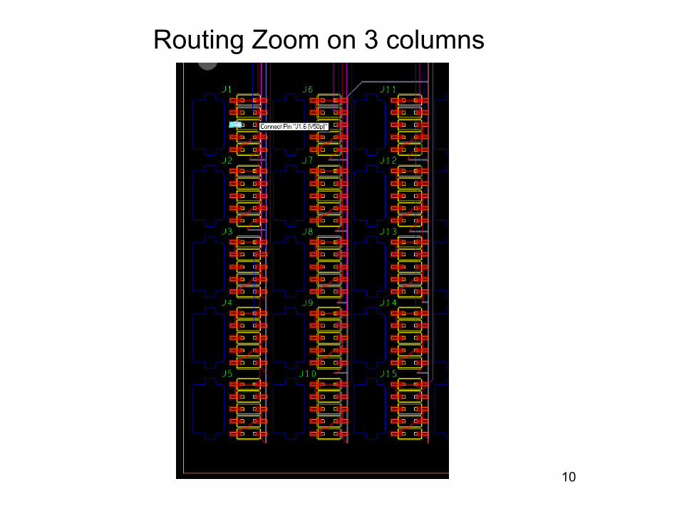
Routing Zoom on 3 columns

11
• Mechanical Specifications with Orsay Done!• Design of LEFT TOP and LEFT BOTTOM boards Done!• Layout routing of LEFT TOP and LEFT BOTTOM boards in progress• Left T/B Boards purchase requisition
November• Design of RIGHT TOP and RIGHT BOTTOM boards with the correct
HV grouping November • Layout routing of RIGHT TOP and RIGHT BOTTOM boards.
December • Test Left T/B Electrical connections and Full crosstalk December • Board Productions and Assembly (with the same company serving the
FT-Cal). 12k euro January 2014
• Test on Electrical connections and Full crosstalk test with FT-Cal crystals 3k euro Mid February 2014
HPS Motherboard WorkPlan