enjoy this joke boring lectures 无聊的课 one of my favorite teachers at southeast missouri state...
TRANSCRIPT

Enjoy this jokeEnjoy this jokeBoring lecturesBoring lectures
无聊的课无聊的课One of my favorite teachers at Southeast Missouri One of my favorite teachers at Southeast Missouri State University in Cape Girardeau is known for State University in Cape Girardeau is known for his droll sense of humor. Explaining his ground ruhis droll sense of humor. Explaining his ground rules to one freshman class, he said, "Now I know mles to one freshman class, he said, "Now I know my lectures can often be dry and boring, so I don't y lectures can often be dry and boring, so I don't mind if you look at your watches during class. I dmind if you look at your watches during class. I do, however, object to your pounding them on the do, however, object to your pounding them on the desk to make sure they're running!"esk to make sure they're running!"


reviewreview : : Chapter 9Chapter 9 Electrooptic modulatio Electrooptic modulation of laser beamsn of laser beams

1. Please read the following 1. Please read the following Keywords loudly, and then Keywords loudly, and then
translate into Chinese.translate into Chinese.①① Electrooptic Modulation Electrooptic Modulation 电光调制电光调制②② electrooptic coefficient electrooptic coefficient 电光系数电光系数③③ electrooptic constant electrooptic constant 电光常数电光常数④④ electrooptic tensor electrooptic tensor 电光张量电光张量⑤⑤ electrooptical birefringence electrooptical birefringence 电光双折射电光双折射⑥⑥ electrooptical anisotropy electrooptical anisotropy 电学、光学各向异性现象电学、光学各向异性现象
⑦⑦ electrooptic effectelectrooptic effect
⑧⑧ electrooptic retardationelectrooptic retardation
电光效应电光效应
电光延迟电光延迟

2.Using table 92.Using table 9 -- 1, determine t1, determine the lectrooptic tensor of KDP cryhe lectrooptic tensor of KDP crystalstal
41
41
63
0 0 0
0 0 0
0 0 0
0 0
0 0
0 0
ijr r
r
r

E Z��������������
0,x yE E
2 2 2
41 41 632 2 22 2 2 1x y z
o o e
x y zr E yz r E xz r E xy
n n n
2 2 2
632 2 22 1z
o o e
x y zr E xy
n n n becomes
To be specific we choose the direction of the applied field parallel to the Z axis,
so the index ellipsoid for KDP

22 2
63 632 2 20 0
1 1' ' 1z z
e
zr E x r E y
n n n
2 2 2
632 20
1ze
x y zr E xy
n n
2 2 2
2 2 21
x y z
x y z
n n n
0 0
0 0
'cos 45 'sin 45
'sin 45 'cos 45
x x y
y x y
Find a new coordinate system:

x
ellipse formed by the intersection of the plane z=0 and the ellipsoid.
x' y'
450
y
The equation of this ellipse 2 2
63 632 20 0
1 1' ' 1z zr E x r E y
n n

The difference of at the output plane z=L between two components is called the retardation .
phase
At point a, the retardation is 0 and the field is linearly At point a, the retardation is 0 and the field is linearly polarized along x.polarized along x.
2
'z
x
E l V
V V
9.2-6'y
Retardation
At point e, , the electric field vector is At point e, , the electric field vector is circularly polarized.circularly polarized.

.At point I, , and the radiation is again linearly polarized, but this time along the y axis---that is, at 900 to its input direction of polarization.

9.3 electrooptic amplitude modulation9.3 electrooptic amplitude modulation
An examination of figure 9-3 reveals that the electrically induced birefringence causes a wave launched at z=0 with its polarization along x to acquire a y polarization, which grows with distance at the expense of the x component until at point i, at which , the polarization becomes parallel to y, if point i corresponds to the output plane of the crystal and if one inserts at this point a polarizer at right angles to the input polarization---that is, one that allows only to pass---then with the field on, the optical beam passes through unattenuated ( 无衰减的 ), whereas with the field off ( ), the output beam is blocked off completely by the crossed output polarizer. This control of the optical energy flow serves as the basis of the electrooptic amplitude modulation of light.
yE
0
显示
双折射
发射

Figure 9.4 A typical arrangement of an electrooptic amplitude modulation
It consists of an electrooptic crystal placed between two crossed polarizers.

To be specific, we show how this arrangement is achieved using a KDP crystal. Also included in the optical path is a naturally birefringent crystal that introduces a fixed retardation, so the total retardation is the sum of the retardation due to this crystal and the electrically induced one. The incident field is parallel to x at the input face of the crystal, thus having equal-in-phase components along x′ and y′ that we take as:
' cosxe A t
' cosye A t

Three missionsThree missions
0
mission : ?yone E
mission : ?o y otwo I I
mission : ? , !o
i
Ithree discuss
I

Using the complex amplitude notation( 符号 ):
' (0)xE A'(0)yE A
The incident intensity is thus becomes
22* 2' '(0) (0) 2i x yI E E A E E
'
'
ix
y
E l Ae
E l A
Upon emerging from the output face z=l , the x′ and y′ components have acquired a relative phase shift (retardation) of radians ( 弧度 )
9.3-1
9.3-2
0
?yE
0
mission : ?yone E

x
y
Y’X’
45o45o
0 0'sin 45 'cos 45y x y
' '00 0
sin 45 cos 45
12
y x y
i
E E E
Ae
'
'
ix
y
E l Ae
E l A
Mission one completed

cos ,2
ix ixe ex
1 cossin
2 2
x x
note :
: ?o y oHave a try I I
mission : ?o y otwo I I

*
2 2
22
2 2
1 12 2
1 2 22 2 2
2 2cos( ) 1 cos( )2
2 sin2
o y y yo o o
i i
i ii i i i
I I
A Ae e
A A e ee e e e
AA
A
E E
Which corresponds to an output intensity:
2 20 2 sin
2I A
9.3-6

The ratio of the output intensity to the input is thus:
2 1 cossin
2 2O
i
I
I
2 20 2 sin
2I A
9.3-6
9.3-7
mission : ? , !o
i
Ithree discuss
I
22* 2' '(0) (0) 2i x yI E E A E E 9.3-1

discussdiscuss
sin ,o
i
I V
I V
thus:
Sinusoidal modulation voltageSinusoidal modulation voltage sin ,m mV V t
sin ( / )i
I
I
sin sino mm
i
I Vt
I V
then
zE l V
V V
9.2-6
1. Without “quarter wave 1. Without “quarter wave plate” insertedplate” inserted
Linear modulation?
Frequenceis identical?

discussdiscuss
2. “quarter wave plate” 2. “quarter wave plate” insertedinserted
sinsin
2 2m m
m m
V tt
V
mm
V
V
2 2sin sin sin2 4 2 2
1 cos( sin ) 12 2 1 sin sin2 2 2
o mm
i
m m
m m
It
I
tt
9.3-7

For For 1mm
V
V
11 sin sin
2
11 sin
2
om m
i
m m
It
I
t
0limsinx
x x
The intersity modulation is a linear replica of the modulating voltage sinm mV V t

Figure 9.5 Transmission factor of a cross-polarized electrooptic modulator as a funtion of an applied voltage.
The modulator is biased to the point . A small applied sinusoidal voltage modulates the transmitted intensity about the bias point.
/ 2m
analog modulation

digital modulation

digital modulation

1,.................
9.3
mm
VIf
V
discussed in problem

Figure 9.6 An optical communication link using an electrooptic modulator
留声机 , 电唱机
光强度探测器

Exercise one: Exercise one: Page:367 Page:367 problem 9.3problem 9.3
Use the Bessel-function expansion of sin (aUse the Bessel-function expansion of sin (asin(x)) to express (9.3-7) in terms of the hasin(x)) to express (9.3-7) in terms of the harmonics of the modulation frequency .rmonics of the modulation frequency .Plot the ratio of the third harmonic ( ) of Plot the ratio of the third harmonic ( ) of the output intensity to the fundamental as the output intensity to the fundamental as a function of . What is the maximum ala function of . What is the maximum allowed if this ratio is not to exceed 10lowed if this ratio is not to exceed 10-2-2
m3 m
m
m
1 3
2 10
sin( sin ) 2 ( )sin 2 ( )sin 3
2 ( )sin(2 1)
m m m m m m
n m mn
t J t J t
J n t
1 3( )si1 1
1 sin sin2 2 2
n ( )sin 3mmi
mo
m mm J t J tI
tI
tips!


When , the third harmonicthe third harmonic is neglectable0.5m rad

If , then J1 (1)=0.44, J3(1)=0.02,
So
1m rad
3
1
(1)0.045
(1)
J
J
1m rad Linear modulation condition:

sin2D m m D
VV V V t where V
Can it be removed?Any other alternative?
Exercise two: Consider such an applied alternating current
Please derive the expression for transmission factor.
可供选择的办法

实验仪器
全反镜
电光晶体 偏振片 聚光腔
输出镜4
镀全反染料盒
输出镜调Q模块
染料调Q激光器
聚光腔
电光调Q激光器

9.4 phase modulation of light9.4 phase modulation of light
The incident beam is polarized parallel to one of them, x′ ray. In this case the application of the electric field does not change the state of polarization, but merely changes the output phase by
' /x x
ln
c
9.4-1


Where:
'
363
2o
zx
n rE l
c
If the bias field is sinusoidal and is taken as :
sinz mE E t then an incident optical field, which at the input (z=0) face of the crystal is given by
exp( )ine A i t
9.4-2
9.4-3
9.4-4

will emerge as :3
63exp{ [ ( sin ) ]}2o
out o m
ne A i t n r E t l
c
where l is the length of the crystal. Dropping the constant phase factor, which is of no consequence here, we rewrite the last equation as :
exp[ ( sin )]out me A i t t
where3
63o mn r E l
9.4-5
9.4-6

is referred to as the phase modulation index. The optical field is thus phase-modulated with a modulation index . If we use the Bessel function identity ( 贝塞尔函数恒等式 )
exp( sin ) ( ) exp( )m n mn
i t J in t
so
( )( ) mi n tout n
n
e A J e
which form gives the distribution of energy in the sidebands as a function of the modulation index . We note that, for , and .
0 0 (0) 1J ( ) 0, 0nJ n
9.4-8
9.4-9

图 6.5 电光相位调制器的基本原理框图
²¨µ¼
LiNbO 3¹âÊäÈë Òѵ÷¹âÊä³ö
³¤¶ÈL
µçѹ

6.3.2 M6.3.2 M--ZZ 型调制器型调制器 MM--ZZ 型调制器是由一个型调制器是由一个 YY 型分路型分路
器、 两个相位调制器和器、 两个相位调制器和 YY 型合路器组成型合路器组成的, 其结构如图的, 其结构如图 6.66.6 所示。 相位调制器所示。 相位调制器就是上述的电折射调制器。 输入光信号就是上述的电折射调制器。 输入光信号被被 YY 型分路器分成完全相同的两部分, 型分路器分成完全相同的两部分, 两个部分之一受到相位调制, 然后两部两个部分之一受到相位调制, 然后两部分再由分再由 YY 型合路器耦合起来。 按照信号型合路器耦合起来。 按照信号之间的相位差, 两路信号在之间的相位差, 两路信号在 YY 型合路器型合路器的输出产生相消和相长干涉, 就得到了的输出产生相消和相长干涉, 就得到了“通”和“断”的信号。 “通”和“断”的信号。

图 6.6 M-Z 型调制器
¹âÊäÈëÒѵ÷¹âÊä³ö
LiNbO 3
´¥µã
´¥µã
Ïàλµ÷ÖÆ

9.5 transverse electrooptic modulation9.5 transverse electrooptic modulation
In the example of electrooptic retardation discussed in the two preceding sections, the electric field was applied along the direction of light propagation. This is the so-called longitudinal mode of modulation. A more desirable mode of operation is the transverse one, in which the field is applied normal to the direction of propagation. The reason is that in this case the field electrodes do not interfere with the optical beam, and the retardation, being proportional to the product of the field times the crystal length, can be increased by the use of longer crystals.

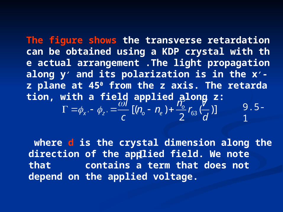
The figure shows the transverse retardation can be obtained using a KDP crystal with the actual arrangement .The light propagation along y′ and its polarization is in the x′-z plane at 450 from the z axis. The retardation, with a field applied along z:
3
' ' 63[( ) ( )]2o
x z o e
nl Vn n r
c d
where d is the crystal dimension along the direction of the applied field. We note that contains a term that does not depend on the applied voltage.
9.5-1

9.6 high-frequency modulation considerations9.6 high-frequency modulation considerations
In the examples considered in the three preceding sections, we derived expressions for the retardation caused by electric field of low frequencies. In many practical situations the modulation signal is often at very high frequencies and, in order to utilize the wide frequency spectrum available with lasers, may occupy a large band-width. In this section we consider some of the typical experimental situations.

Figure 9-9 Equivalent circuit of an electrooptic modulation crystal in a parallel-plate configuration
/ 2o The electrooptic crystal is placed between two electrodes with a modulation field containing frequencies near applied to it. Rs is the internal resistance ( 内阻 ) of the modulation source and C represents the parallel-plate capacitance due to the electrooptic crystal.

1. If , most of the modulation voltage drop is across and is thus wasted, since it does not contribute to the retardation. This can be remedied by resonating ( 共振 ) the crystal capacitance with an inductance L, where
2. A shunting resistance is used so that at the impedance of the parallel RLC circuit is , which is chosen to be larger than so most of the modulation voltage appears across the crystal. The resonant circuit has a finite band-width ---that is, its impedance is high only over a frequency interval
(centered on ).
3. The maximum modulation bandwidth must be less then
1( )s oR C sR
2 1( )o LC
LR o
LRsR
/ 2 1/ 2 LR C
/ 2 1/ 2 LR C

Schoolwork:
1. study the contents of transit-time limitations to High-Frequency Eletrooptic Modulation.
2. Show that ,if a phase-modulated optical wave is incident on a square-law detector, the output contains no alternating currents
???