fet freq
TRANSCRIPT
8/9/2019 Fet Freq
http://slidepdf.com/reader/full/fet-freq 1/2
EEE 132 FET High Frequency Models 1
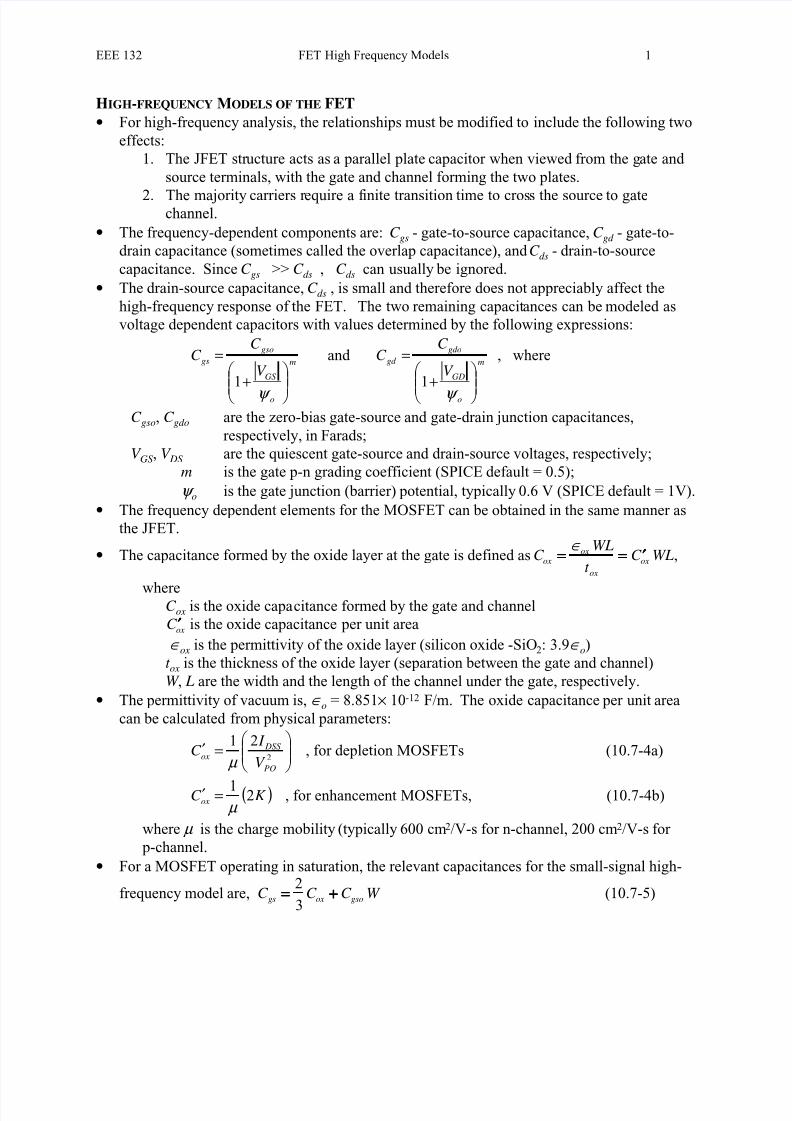
H IGH -FREQUENCY M ODELS OF THE FET• For high-frequency analysis, the relationships must be modified to include the following two
effects:1. The JFET structure acts as a parallel plate capacitor when viewed from the gate and
source terminals, with the gate and channel forming the two plates.
2. The majority carriers require a finite transition time to cross the source to gatechannel.
• The frequency-dependent components are: C gs - gate-to-source capacitance, C gd - gate-to-drain capacitance (sometimes called the overlap capacitance), and C ds - drain-to-sourcecapacitance. Since C gs >> C ds , C ds can usually be ignored.
• The drain-source capacitance, C ds , is small and therefore does not appreciably affect thehigh-frequency response of the FET. The two remaining capacitances can be modeled asvoltage dependent capacitors with values determined by the following expressions:
m
o
GS
gsogs
V
C C
+
=
ψ 1
and m
o
GD
gdogd
V
C C
+
=
ψ 1
, where
C gso , C gdo are the zero-bias gate-source and gate-drain junction capacitances,respectively, in Farads;
V GS , V DS are the quiescent gate-source and drain-source voltages, respectively;m is the gate p-n grading coefficient (SPICE default = 0.5);ψ o is the gate junction (barrier) potential, typically 0.6 V (SPICE default = 1V).
• The frequency dependent elements for the MOSFET can be obtained in the same manner asthe JFET.
• The capacitance formed by the oxide layer at the gate is defined as C WL
t C WLox
ox
oxox
==== ==== ′′′′∈ ,
whereC ox is the oxide capacitance formed by the gate and channel
′′′′C ox is the oxide capacitance per unit area∈ox is the permittivity of the oxide layer (silicon oxide -SiO 2: 3.9∈o)
t ox is the thickness of the oxide layer (separation between the gate and channel)W , L are the width and the length of the channel under the gate, respectively.
• The permittivity of vacuum is, ∈o = 8.851 × 10 -12 F/m. The oxide capacitance per unit areacan be calculated from physical parameters:
=′
2
21
PO
DSS ox V
I C
µ , for depletion MOSFETs (10.7-4a)
( )K C ox 21 µ
=′ , for enhancement MOSFETs, (10.7-4b)
where µ is the charge mobility (typically 600 cm 2/V-s for n-channel, 200 cm 2/V-s for p-channel.
• For a MOSFET operating in saturation, the relevant capacitances for the small-signal high-
frequency model are, C C C W gs ox gso==== ++++2
3 (10.7-5)

8/9/2019 Fet Freq
http://slidepdf.com/reader/full/fet-freq 2/2
EEE 132 FET High Frequency Models 2
and C C W gd gdo==== , (10.7-6)
where C gso ,C gdo are the zero bias gate-source and gate drain capacitances, respectively(typically C gso = C gdo = 3 × 10 -12 F/m), and are related to ′′′′C ox .
• The capacitances in the high-frequency small-signal model of the MOSFET are relativelyconstant over the frequency range.
• Note also that the MOSFET zero bias capacitance has dimensions of F/m and in the JFET, it has units of F.
• Although the values of the components are different, the JFET and MOSFET share the samesmall-signal model arrangement shown in Figure 10.7-1.
C gd
C ds
C gs r
d
gmv
gsv
o
++
− −
vgs
Figure 10.7-1. Accurate FET High-frequency Model
• Since C ds is small compared to C gs, the drain-source capacitance may be ignored in mostanalysis and design situations, and the simplified model shown in Figure 10.7-2 may be used.
C gd
C gs r
d
gmv
gsvo
++
− −
vgs
Figure 10.7-2. Simplified FET High-frequency Model
• Circuit parameters, at specific bias conditions, obtained from the manufacturers' data sheets isusually provided in terms of y- parameters: the common-source short-circuit input capacitanceC iss , reverse transfer capacitance C rss , and output capacitance, C oss are provided:
C gd ≈ C rss (10.7-7)C gs
≈ C iss - C rss (10.7-8)C ds ≈ C oss - C rss (10.7-9)
• The maximum operating frequency, ω T , is the frequency at which the FET no longeramplifies the input signal: that is, the dependent current source gmvgs is equal to the inputcurrent.
( )dsgs
mT C C
g+
=ω . (10.7-10)
• In general, BJTs have higher maximum operating frequencies than FETs. Two factors areresponsible for the lower frequency performance of FETs compared to BJTs:
◊ For a given area and operating current, the gm of silicon FETs are less than half ofsilicon BJTs.
◊ In MOSFET structures, considerable capacitance is observed at the input due to theoxide layer. In JFETs, semiconductor properties and physical dimensions of thedevice result long channel lengths that reduce high-frequency performance.