logic synthesis - viplab.cs.nctu.edu.twviplab.cs.nctu.edu.tw/course/dcl2019_fall/dcl_mat_03.pdf ·...
TRANSCRIPT
1
Synthesis Training Course
Logic Synthesis
TSRI 楊智喬
Synthesis Training Course
Outline
Introduction to Cell-based Design Flow
Logic Synthesis
Introduction to Logic Synthesis
Coding Style for Synthesis
Static Timing Analysis
Synopsys Design Compiler
SDF and Gate-Level Simulation
2
2
Synthesis Training Course
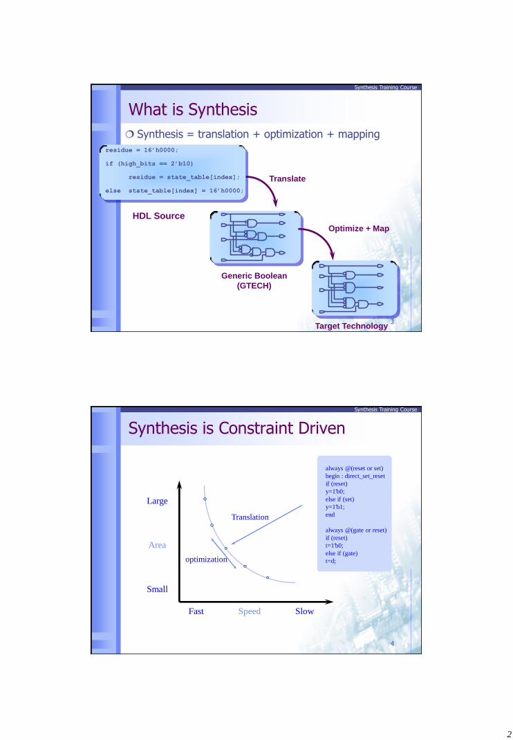
What is Synthesis
Synthesis = translation + optimization + mapping
HDL Source
Generic Boolean
(GTECH)
Translate
Target Technology
Optimize + Map
residue = 16’h0000;
if (high_bits == 2’b10)
residue = state_table[index];
else state_table[index] = 16’h0000;
3
Synthesis Training Course
Synthesis is Constraint Driven
optimization
Large
Area
Small
Fast Speed Slow
Translation
always @(reset or set)
begin : direct_set_reset
if (reset)
y=1'b0;
else if (set)
y=1'b1;
end
always @(gate or reset)
if (reset)
t=1'b0;
else if (gate)
t=d;
4
3
Synthesis Training Course
Technology Independent
Design can be transferred to any technology
Large
Area
Small
Fast Speed Slow
Technology A
Technology B
RTL
5
Synthesis Training Course
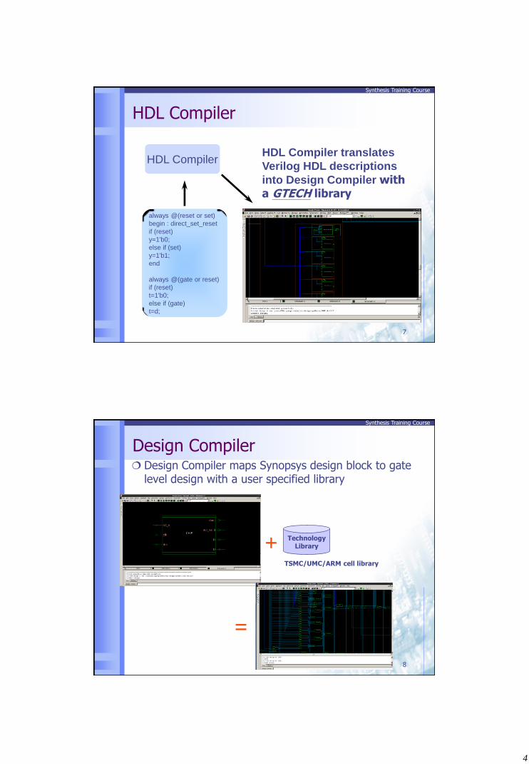
Logic Synthesis Overview
RTL Design
HDL
Compiler
Design
Compiler
Optimized
Gate-level Netlist
DW
Developer
Lib
Compiler
Architecture
Optimization
Logic
Optimization
Design Ware Library
Technology Library
6
4
Synthesis Training Course
HDL Compiler
HDL Compiler HDL Compiler translates
Verilog HDL descriptions
into Design Compiler with a GTECH library
always @(reset or set)
begin : direct_set_reset
if (reset)
y=1'b0;
else if (set)
y=1'b1;
end
always @(gate or reset)
if (reset)
t=1'b0;
else if (gate)
t=d;
7
Synthesis Training Course
Design Compiler Design Compiler maps Synopsys design block to gate
level design with a user specified library
+
=
Technology Library
TSMC/UMC/ARM cell library
8
5
Synthesis Training Course
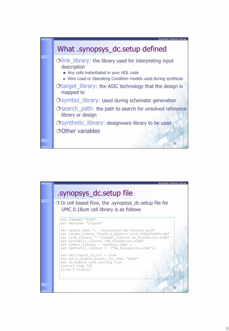
What .synopsys_dc.setup defined
link_library: the library used for interpreting input
description Any cells instantiated in your HDL code
Wire Load or Operating Condition models used during synthesis
target_library: the ASIC technology that the design is
mapped to
symbol_library: used during schematic generation
search_path: the path to search for unsolved reference
library or design
synthetic_library: designware library to be used
Other variables
9
Synthesis Training Course
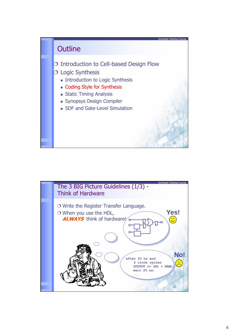
.synopsys_dc.setup file
In cell based flow, the .synopsys_dc.setup file for
UMC 0.18um cell library is as follows
set COMPANY “TSRI”
set designer “ccyang”
set search_path “. ~/SynopsysDC/db $search_path”
set target_libary “fsa0m_a_generic_core_fflp98vm40c.db”
set link_library “* $target_library dw_foundation.sldb”
set synthetic_library “dw_foundation.sldb”
set symbol_library = {generic.sdb} ;
set synthetic_library = {“dw_foundation.sldb”};
set verilogout_no_tri = true
set hdlin_enable_presto_for_vhdl “TRUE”
set sh_enable_line_editing true
history keep 100
alias h history
10
6
Synthesis Training Course
Outline
Introduction to Cell-based Design Flow
Logic Synthesis
Introduction to Logic Synthesis
Coding Style for Synthesis
Static Timing Analysis
Synopsys Design Compiler
SDF and Gate-Level Simulation
11
Synthesis Training Course
The 3 BIG Picture Guidelines (1/3) - Think of Hardware
Write the Register Transfer Language.
When you use the HDL, ALWAYS think of hardware!
after 20 ns and
2 clock cycles
OUTPUT <= IN1 + RAM1;
wait 20 ns;
...
Yes!
No!
12
7
Synthesis Training Course
The 3 BIG Picture Guidelines (2/3) - Think of Synchronous Hardware
Synchronous design can run smoothly during synthesis, test , simulation and layout.
Asynchronous design should be avoided as possible!
ADDR DECODE
ADDR_IN
ACK
ACK_SET
AS
+5
ACK_CLR
How am I going to
synthesize this?
13
Synthesis Training Course
The 3 BIG Picture Guidelines (3/3) - Think RTL
RTL = Register Transfer Level
Writing in an RTL coding style means describing
the register architecture,
the circuit topology, and
the functionality between registers
Design Compiler optimizes logic between registers
It does not optimize the register placement
14
8
Synthesis Training Course
Synthesizable Verilog Code
Synopsys can’t accept all kinds of Verilog
constructs
Synopsys can only accept a subset of Verilog syntax and this subset is called “Synthesizable Verilog Code”
The same situation also exists in VHDL
This chapter will introduce synthesizable verilog coding style to you, and this is the first challenge when you use Synopsys to convert your RTL code to Gate level netlist
15
Synthesis Training Course
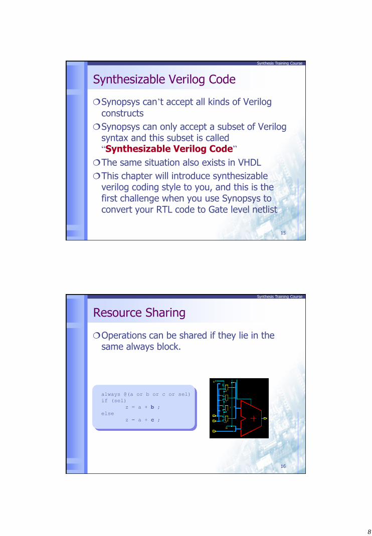
Resource Sharing
Operations can be shared if they lie in the same always block.
always @(a or b or c or sel)
if (sel)
z = a + b ;
else
z = a + c ;
16
9
Synthesis Training Course
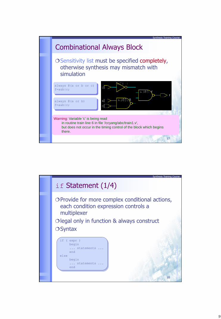
Combinational Always Block
Sensitivity list must be specified completely, otherwise synthesis may mismatch with simulation
always @(a or b or c)
f=a&b|c;
always @(a or b)
f=a&b|c;
Warning: Variable 'c' is being read
in routine train line 6 in file '/ccyang/abc/train1.v',
but does not occur in the timing control of the block which begins
there.
17
Synthesis Training Course
if Statement (1/4)
Provide for more complex conditional actions, each condition expression controls a multiplexer
legal only in function & always construct
Syntax
if ( expr )
begin
... statements ...
end
else
begin
... statements ...
end
18
10
Synthesis Training Course
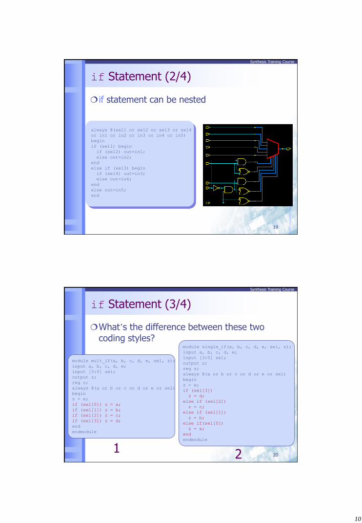
if Statement (2/4)
if statement can be nested
always @(sel1 or sel2 or sel3 or sel4
or in1 or in2 or in3 or in4 or in5)
begin
if (sel1) begin
if (sel2) out=in1;
else out=in2;
end
else if (sel3) begin
if (sel4) out=in3;
else out=in4;
end
else out=in5;
end
19
Synthesis Training Course
if Statement (3/4)
What’s the difference between these two
coding styles?
module mult_if(a, b, c, d, e, sel, z);
input a, b, c, d, e;
input [3:0] sel;
output z;
reg z;
always @(a or b or c or d or e or sel)
begin
z = e;
if (sel[0]) z = a;
if (sel[1]) z = b;
if (sel[2]) z = c;
if (sel[3]) z = d;
end
endmodule
module single_if(a, b, c, d, e, sel, z);
input a, b, c, d, e;
input [3:0] sel;
output z;
reg z;
always @(a or b or c or d or e or sel)
begin
z = e;
if (sel[3])
z = d;
else if (sel[2])
z = c;
else if (sel[1])
z = b;
else if(sel[0])
z = a;
end
endmodule
1 2 20
11
Synthesis Training Course
if Statement (4/4)
1 2
21
Synthesis Training Course
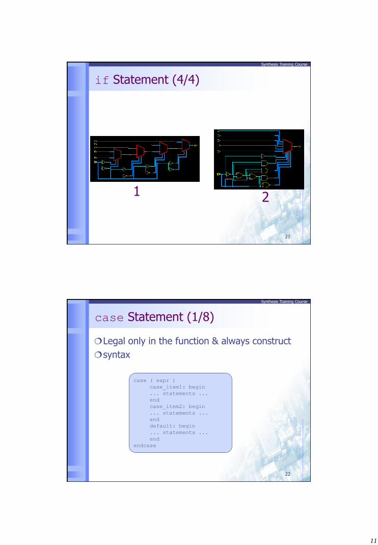
case Statement (1/8)
Legal only in the function & always construct
syntax
case ( expr )
case_item1: begin
... statements ...
end
case_item2: begin
... statements ...
end
default: begin
... statements ...
end
endcase
22
12
Synthesis Training Course
case Statement (2/8)
A case statement is called a full case if all possible branches are specified.
always @(bcd) begin
case (bcd)
4'd0:out=3'b001;
4'd1:out=3'b010;
4'd2:out=3'b100;
default:out=3'bxxx;
endcase
end
23
Synthesis Training Course
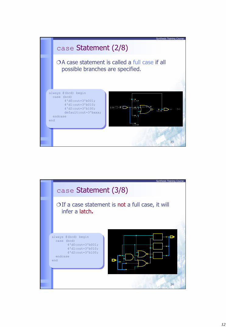
always @(bcd) begin
case (bcd)
4'd0:out=3'b001;
4'd1:out=3'b010;
4'd2:out=3'b100;
endcase
end
case Statement (3/8)
If a case statement is not a full case, it will infer a latch.
24
13
Synthesis Training Course
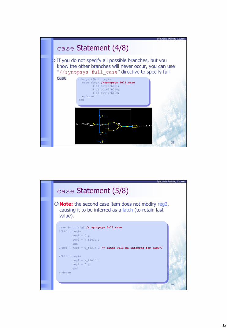
case Statement (4/8)
If you do not specify all possible branches, but you know the other branches will never occur, you can use “//synopsys full_case” directive to specify full
case always @(bcd) begin
case (bcd) //synopsys full_case
4'd0:out=3'b001;
4'd1:out=3'b010;
4'd2:out=3'b100;
endcase
end
25
Synthesis Training Course
case (cntr_sig) // synopsys full_case
2’b00 : begin
reg1 = 0 ;
reg2 = v_field ;
end
2’b01 : reg1 = v_field ; /* latch will be inferred for reg2*/
2’b10 : begin
reg1 = v_field ;
reg2 = 0 ;
end
endcase
Note: the second case item does not modify reg2, causing it to be inferred as a latch (to retain last value).
case Statement (5/8)
26
14
Synthesis Training Course
out = 3’b000 ; // this is called unconditional assignment
case (condition)
…
endcase
case (condition)
…
default : out = 3’b000 ; // out=0 for all other cases
endcase
(1)
(2)
Two possible ways we can assign a default value to
next_state.
case Statement (6/8)
27
Synthesis Training Course
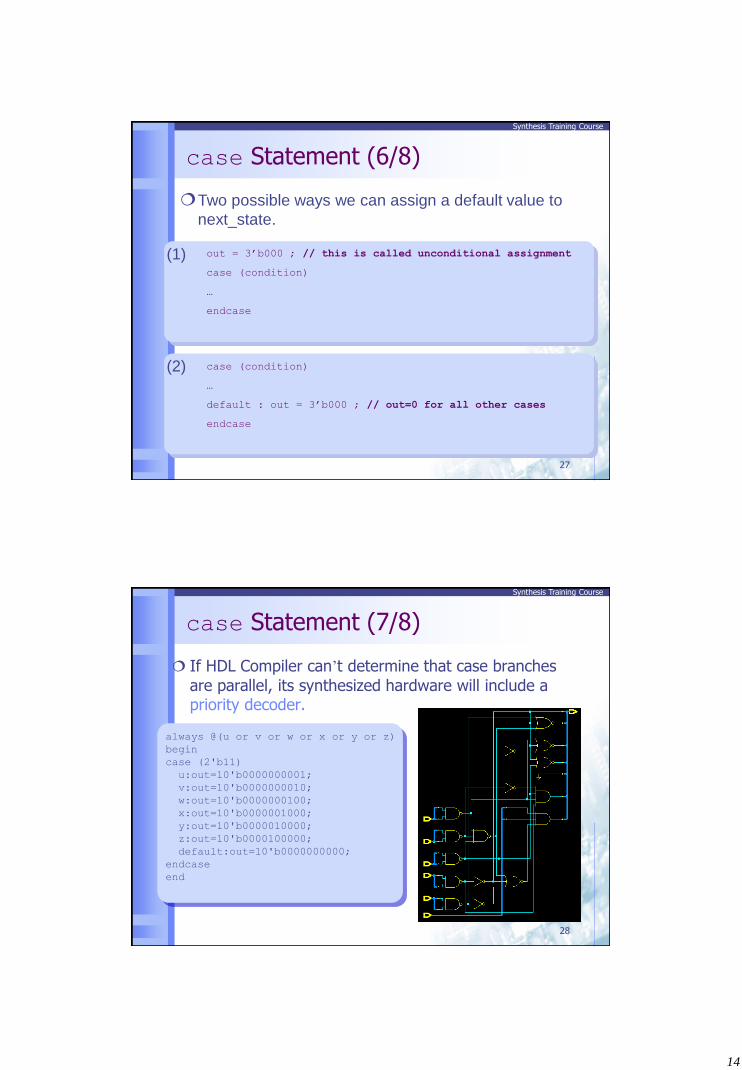
case Statement (7/8)
If HDL Compiler can’t determine that case branches
are parallel, its synthesized hardware will include a priority decoder.
always @(u or v or w or x or y or z)
begin
case (2'b11)
u:out=10'b0000000001;
v:out=10'b0000000010;
w:out=10'b0000000100;
x:out=10'b0000001000;
y:out=10'b0000010000;
z:out=10'b0000100000;
default:out=10'b0000000000;
endcase
end
28
15
Synthesis Training Course
case Statement (8/8)
You can declare a case statement as parallel case with the “//synopsys parallel_case” directive.
always @(u or v or w or x or y or z)
begin
case (2'b11) //synopsys parallel_case
u:out=10'b0000000001;
v:out=10'b0000000010;
w:out=10'b0000000100;
x:out=10'b0000001000;
y:out=10'b0000010000;
z:out=10'b0000100000;
default:out=10'b0000000000;
endcase
end
29
Synthesis Training Course
always Block
Example
If event-expression contains posedge or negedge, flip-flop will be synthesized.
A variable assigned within an always @ block that is not fully specified will result in latches synthesized.
In all other cases, combinational logic will be synthesized.
always @ (event-expression ) begin
statements
end
30
16
Synthesis Training Course
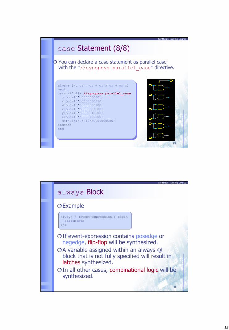
Latch Inference
A variable assigned within an always block that is not fully specified.
always @(a or b or gate) begin
if (gate)
out = a | b ;
end
The conditional expression
becomes the latch enable
31
Synthesis Training Course
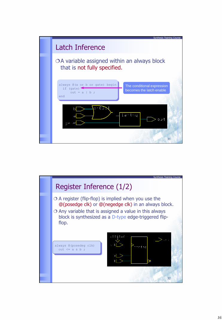
always @(posedeg clk)
out <= a & b ;
Register Inference (1/2)
A register (flip-flop) is implied when you use the @(posedge clk) or @(negedge clk) in an always block.
Any variable that is assigned a value in this always block is synthesized as a D-type edge-triggered flip-flop.
32
17
Synthesis Training Course
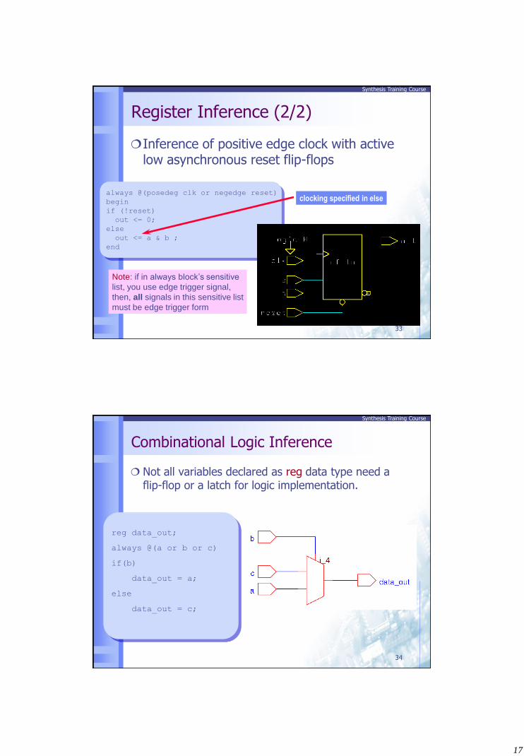
Register Inference (2/2)
Inference of positive edge clock with active low asynchronous reset flip-flops
always @(posedeg clk or negedge reset)
begin
if (!reset)
out <= 0;
else
out <= a & b ;
end
Note: if in always block’s sensitive
list, you use edge trigger signal,
then, all signals in this sensitive list
must be edge trigger form
clocking specified in else
33
Synthesis Training Course
Combinational Logic Inference
Not all variables declared as reg data type need a flip-flop or a latch for logic implementation.
reg data_out;
always @(a or b or c)
if(b)
data_out = a;
else
data_out = c;
34
18
Synthesis Training Course
Outline
Introduction to Cell-based Design Flow
Logic Synthesis
Introduction to Logic Synthesis
Coding Style for Synthesis
Static Timing Analysis
Synopsys Design Compiler
SDF and Gate-Level Simulation
35
Synthesis Training Course
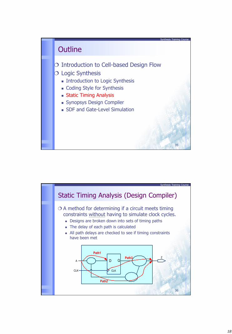
Static Timing Analysis (Design Compiler)
A method for determining if a circuit meets timing constraints without having to simulate clock cycles.
Designs are broken down into sets of timing paths
The delay of each path is calculated
All path delays are checked to see if timing constraints have been met
A
CLK
Z
Path1
Path3
Path2
D Q
CLK
36
19
Synthesis Training Course
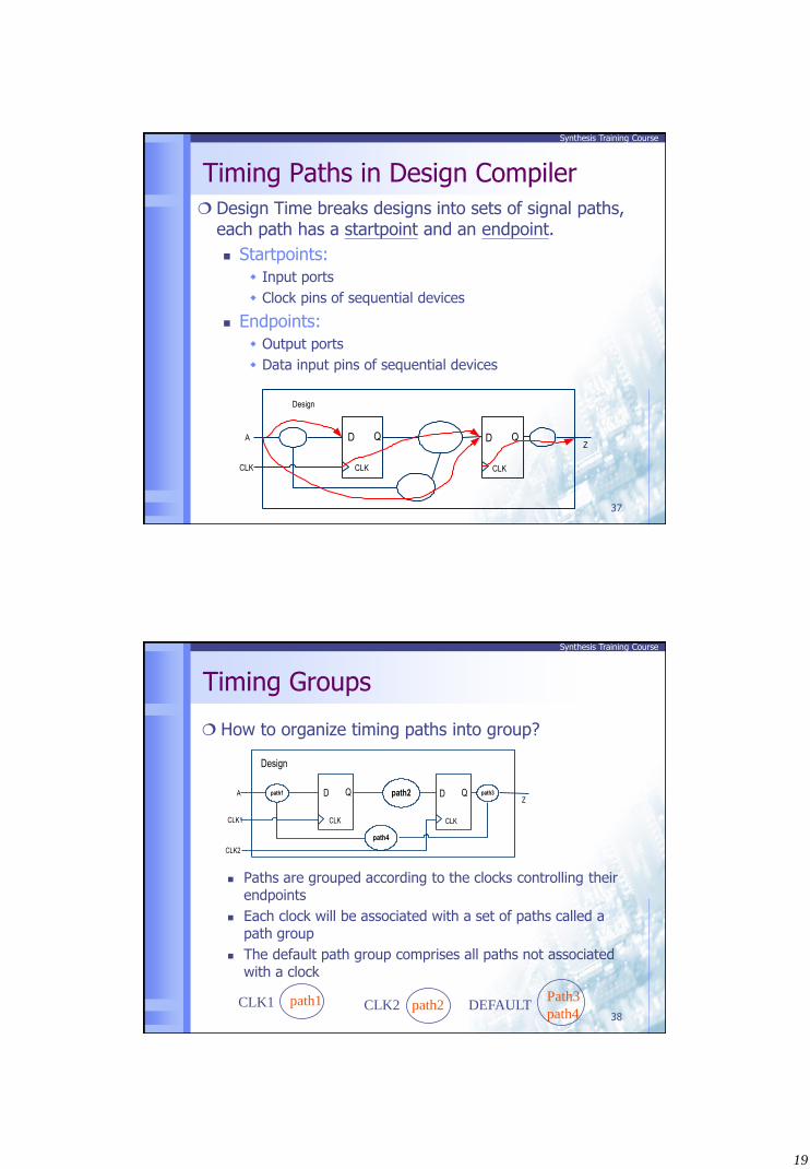
Timing Paths in Design Compiler
Design Time breaks designs into sets of signal paths, each path has a startpoint and an endpoint.
Startpoints:
Input ports
Clock pins of sequential devices
Endpoints:
Output ports
Data input pins of sequential devices
A
CLK
D Q
CLK
D Q
CLK
Z
Design
37
Synthesis Training Course
Timing Groups
How to organize timing paths into group?
Paths are grouped according to the clocks controlling their endpoints
Each clock will be associated with a set of paths called a path group
The default path group comprises all paths not associated with a clock
A
CLK1
D Q
CLK
path2path1
path4
D Q
CLK
path3
Z
Design
CLK2
CLK1 CLK2 DEFAULT path1 path2 Path3
path4 38

20
Synthesis Training Course
Timing Path Exercise
How many timing paths do you see? 11
How many path groups are there? 3
Clock Group1 Clock Group2 Default Clock
D Q
D Q
D Q
D Q
CLK1
CLK2
39
Synthesis Training Course
Schematic Converted To a Timing Graph
To calculate total delay, Design Time breaks each path into timing arcs.
Each timing arc contributes either a net delay or cell delay.
Example of calculating a path delay
All the net and cell timing arcs along the path are added together
D Q
Path Delay = 0.8 + 0.25 + 0.77 + 0.2 + 0.56 +0.11 = 2.51 ns
D Q
0.50.30.660.45
0.430.61
0.72
D Q D Q
CLK
0.8
0.11
0.2
0.56
0.770.25
40
21
Synthesis Training Course
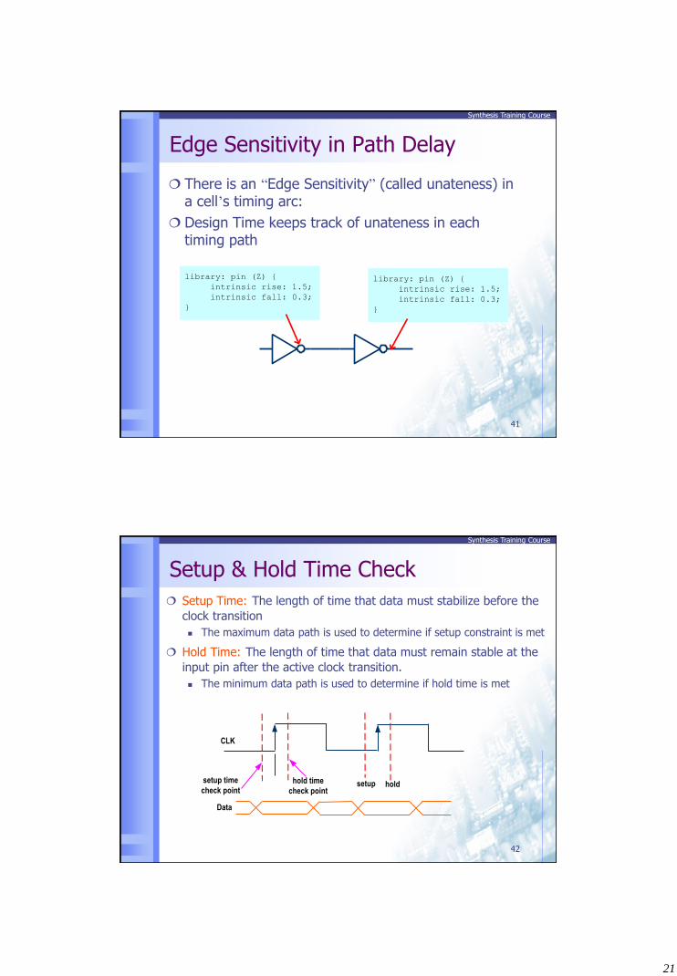
Edge Sensitivity in Path Delay
There is an “Edge Sensitivity” (called unateness) in a cell’s timing arc:
Design Time keeps track of unateness in each timing path
library: pin (Z) {
intrinsic rise: 1.5;
intrinsic fall: 0.3;
}
library: pin (Z) {
intrinsic rise: 1.5;
intrinsic fall: 0.3;
}
41
Synthesis Training Course
Setup & Hold Time Check
Setup Time: The length of time that data must stabilize before the
clock transition
The maximum data path is used to determine if setup constraint is met
Hold Time: The length of time that data must remain stable at the
input pin after the active clock transition.
The minimum data path is used to determine if hold time is met
setup time
check pointhold time
check pointsetup hold
CLK
Data
42
22
Synthesis Training Course
Outline
Introduction to Cell-based Design Flow
Logic Synthesis
Introduction to Logic Synthesis
Coding Style for Synthesis
Static Timing Analysis
Synopsys Design Compiler
SDF and Gate-Level Simulation
43
Synthesis Training Course
Synopsys Graphical Environment
Design Vision
44
23
Synthesis Training Course
Invoke Design Vision
Unix%> design_vision (or dv)
45
Synthesis Training Course
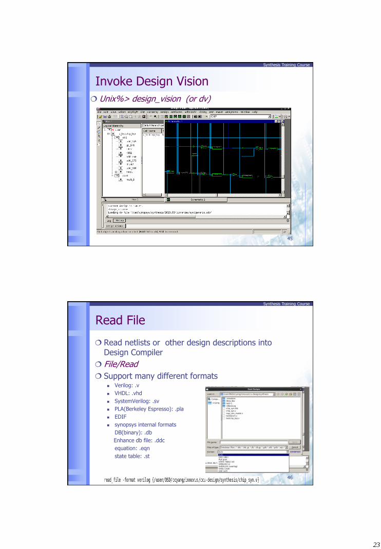
Read File
Read netlists or other design descriptions into Design Compiler
File/Read
Support many different formats Verilog: .v
VHDL: .vhd
SystemVerilog: .sv
PLA(Berkeley Espresso): .pla
EDIF
synopsys internal formats
DB(binary): .db
Enhance db file: .ddc
equation: .eqn
state table: .st
46
24
Synthesis Training Course
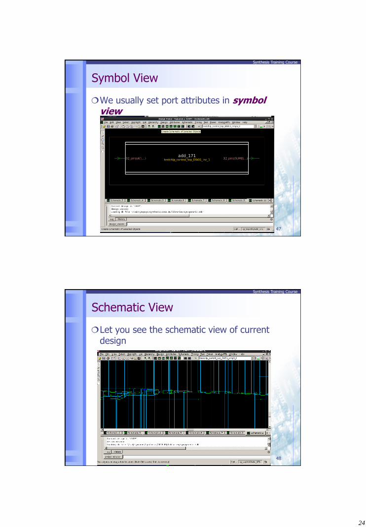
Symbol View
We usually set port attributes in symbol view
47
Synthesis Training Course
Schematic View
Let you see the schematic view of current design
48
25
Synthesis Training Course
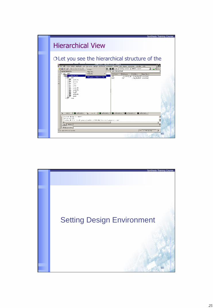
Hierarchical View
Let you see the hierarchical structure of the current design
49
Synthesis Training Course
Setting Design Environment
50
26
Synthesis Training Course
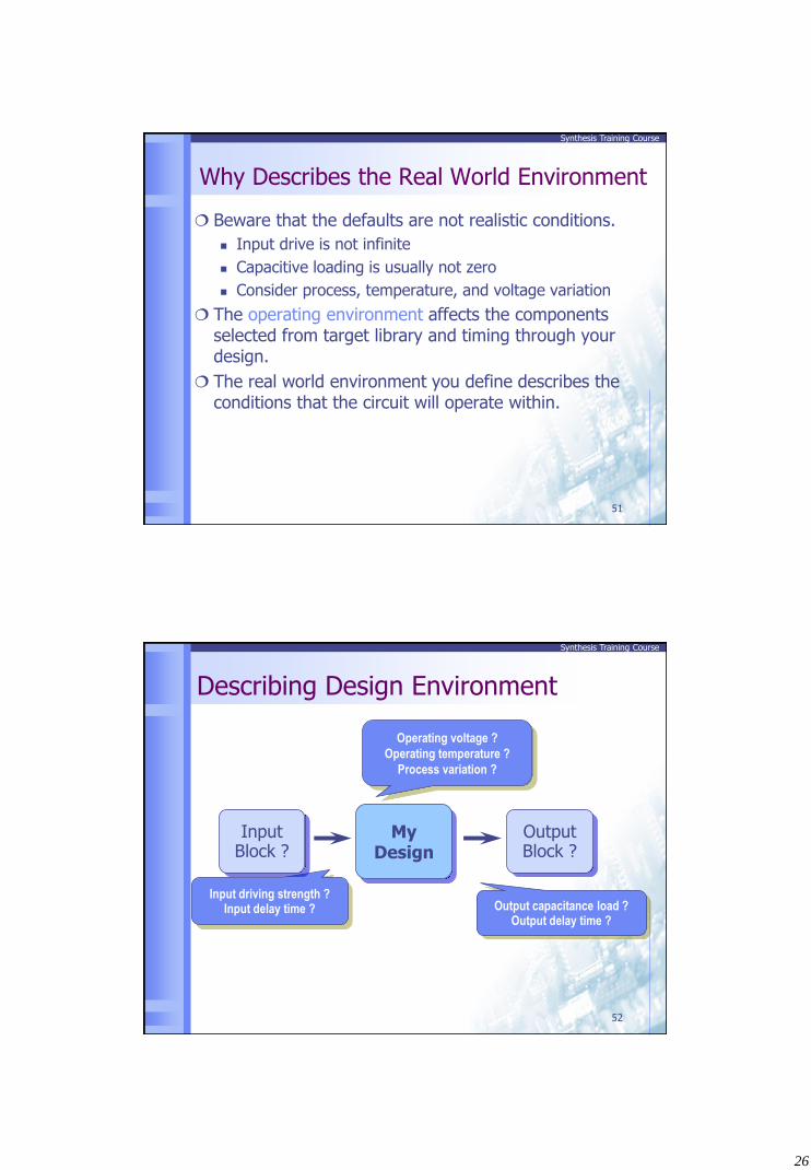
Why Describes the Real World Environment
Beware that the defaults are not realistic conditions.
Input drive is not infinite
Capacitive loading is usually not zero
Consider process, temperature, and voltage variation
The operating environment affects the components selected from target library and timing through your design.
The real world environment you define describes the conditions that the circuit will operate within.
51
Synthesis Training Course
Output capacitance load ? Output delay time ?
Input driving strength ? Input delay time ?
Operating voltage ?
Operating temperature ?
Process variation ?
Describing Design Environment
Input Block ?
My Design
Output Block ?
52
27
Synthesis Training Course
Setting Operating Condition
Attributes/Operating Environment/Operating Condition
design_vision>
53
Synthesis Training Course
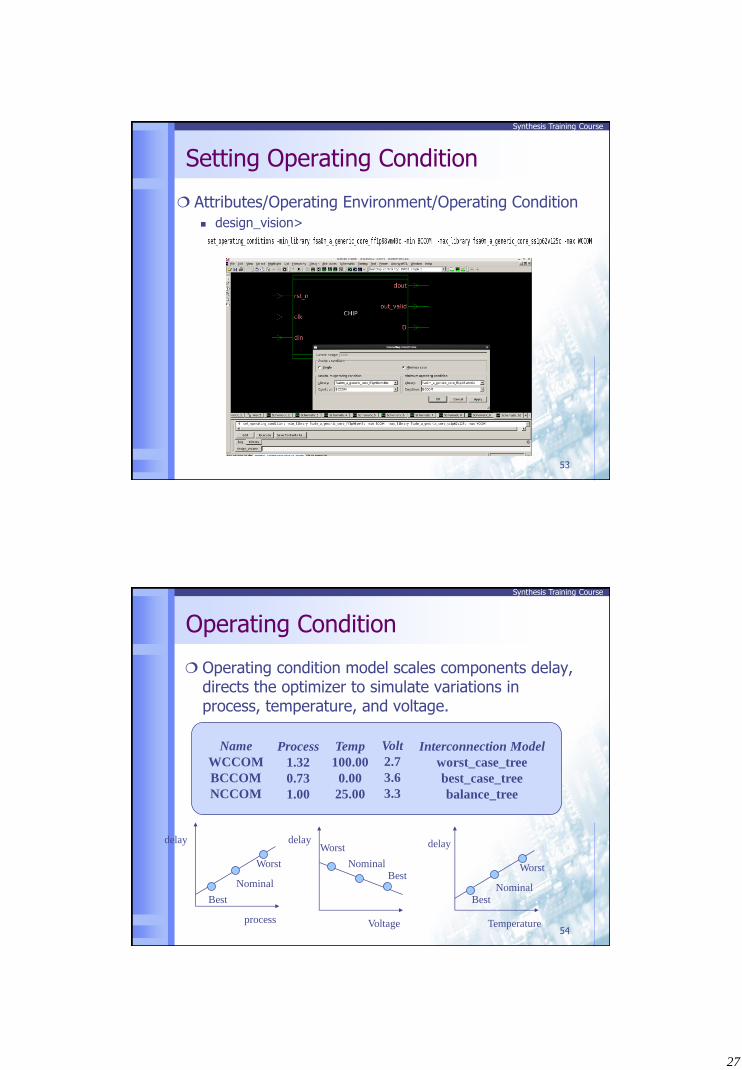
Operating Condition
Operating condition model scales components delay, directs the optimizer to simulate variations in process, temperature, and voltage.
Name
WCCOM
BCCOM
NCCOM
Process
1.32
0.73
1.00
Temp
100.00
0.00
25.00
Volt
2.7
3.6
3.3
Interconnection Model
worst_case_tree
best_case_tree
balance_tree
process
delay
Temperature
delay
Voltage
delay
Best Best
Best Worst Worst
Worst
Nominal Nominal
Nominal
54
28
Synthesis Training Course
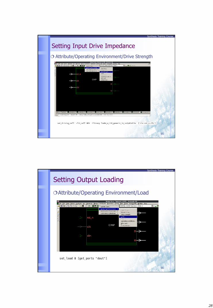
Setting Input Drive Impedance
Attribute/Operating Environment/Drive Strength
55
Synthesis Training Course
Setting Output Loading
Attribute/Operating Environment/Load
56
29
Synthesis Training Course
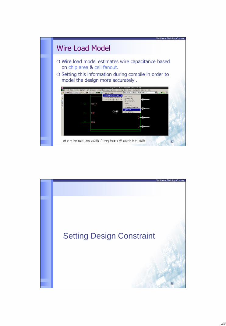
Wire Load Model
Wire load model estimates wire capacitance based on chip area & cell fanout.
Setting this information during compile in order to model the design more accurately .
57
Synthesis Training Course
Setting Design Constraint
58

30
Synthesis Training Course
Constraints
Constraints are goals that the Design Compiler uses for optimizing a design into target technology library.
Design Rule Constraints : technology-specific restriction; ex. maximum transition, maximum fanout, maximum capacitance.
Optimization Constraints : design goals and requirements; ex. maximum delay, minimum delay, maximum area, maximum power.
During compile, Design Compiler attempts to meet all constraints.
59
Synthesis Training Course
Optimization Constraints
Optimization constraints, in order of attentions are
1. Maximum delay
2. Minimum delay
3. (Maximum power)
4. Maximum area
About combinational circuit, we only set maximum delay & minimum delay for timing constraint
60
31
Synthesis Training Course
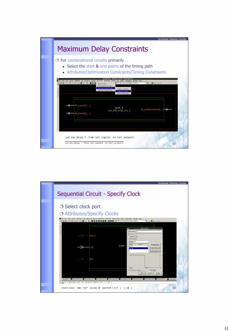
Maximum Delay Constraints
For combinational circuits primarily
Select the start & end points of the timing path
Attributes/Optimization Constraints/Timing Constraints
61
Synthesis Training Course
Sequential Circuit - Specify Clock
Select clock port
Attributes/Specify Clocks
62
32
Synthesis Training Course
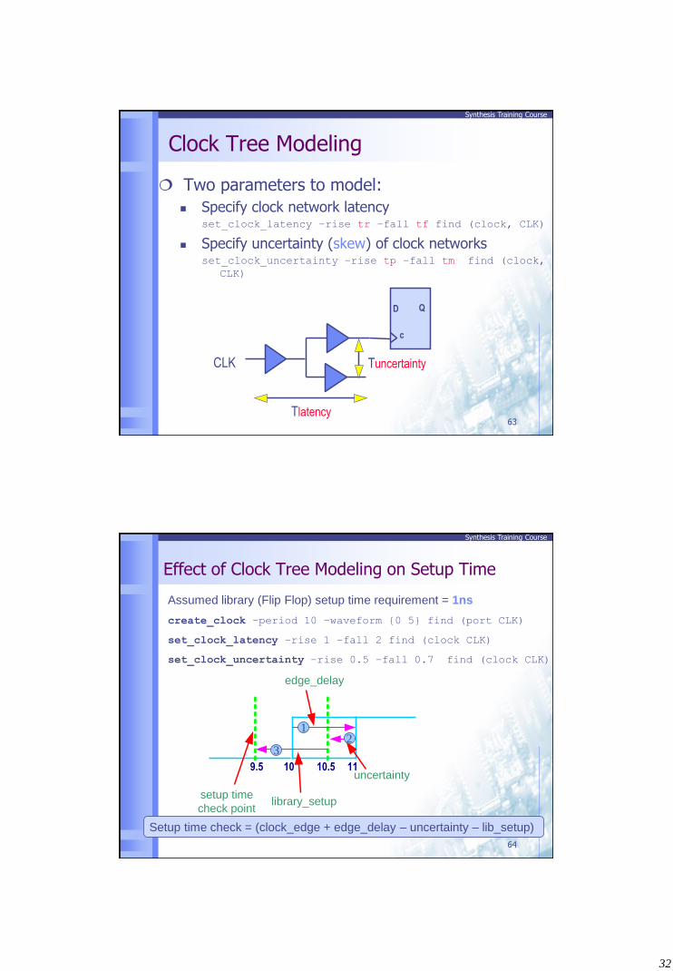
Clock Tree Modeling
Two parameters to model:
Specify clock network latency set_clock_latency –rise tr –fall tf find (clock, CLK)
Specify uncertainty (skew) of clock networks set_clock_uncertainty –rise tp –fall tm find (clock,
CLK)
D Q
CLK
Tlatency
Tuncertainty
c
63
Synthesis Training Course
Effect of Clock Tree Modeling on Setup Time
create_clock –period 10 –waveform {0 5} find (port CLK)
set_clock_latency –rise 1 –fall 2 find (clock CLK)
set_clock_uncertainty –rise 0.5 –fall 0.7 find (clock CLK)
Setup time check = (clock_edge + edge_delay – uncertainty – lib_setup)
setup time
check point
uncertainty
edge_delay
library_setup
10 1110.59.5
1 2
Assumed library (Flip Flop) setup time requirement = 1ns
3
64
33
Synthesis Training Course
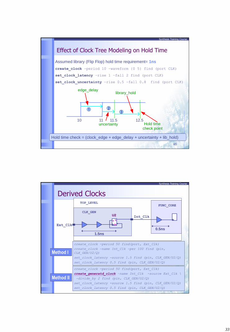
Effect of Clock Tree Modeling on Hold Time
Hold time check = (clock_edge + edge_delay + uncertainty + lib_hold)
create_clock –period 10 –waveform {0 5} find (port CLK)
set_clock_latency –rise 1 –fall 2 find (port CLK)
set_clock_uncertainty –rise 0.5 –fall 0.8 find (port CLK)
Assumed library (Flip Flop) hold time requirement= 1ns
Hold time check point
uncertainty
edge_delay library_hold
10 11 11.5 12.5
1 2 3
65
Synthesis Training Course
1-66
Derived Clocks
create_clock -period 50 find(port, Ext_Clk)
create_clock –name Int_Clk –per 100 find (pin,
CLK_GEN/U2/Q)
set_clock_latency -source 1.5 find (pin, CLK_GEN/U2/Q)
set_clock_latency 0.5 find (pin, CLK_GEN/U2/Q)
create_clock -period 50 find(port, Ext_Clk)
create_generatd_clock –name Int_Clk -source Ext_Clk \
–divide_by 2 find (pin, CLK_GEN/U2/Q)
set_clock_latency -source 1.5 find (pin, CLK_GEN/U2/Q)
set_clock_latency 0.5 find (pin, CLK_GEN/U2/Q)
Q
Qb
D
Ext_Clk
Int_Clk U2
TOP_LEVEL
CLK_GEN
FUNC_CORE
1.5ns
0.5ns
Method I
Method II
34
Synthesis Training Course
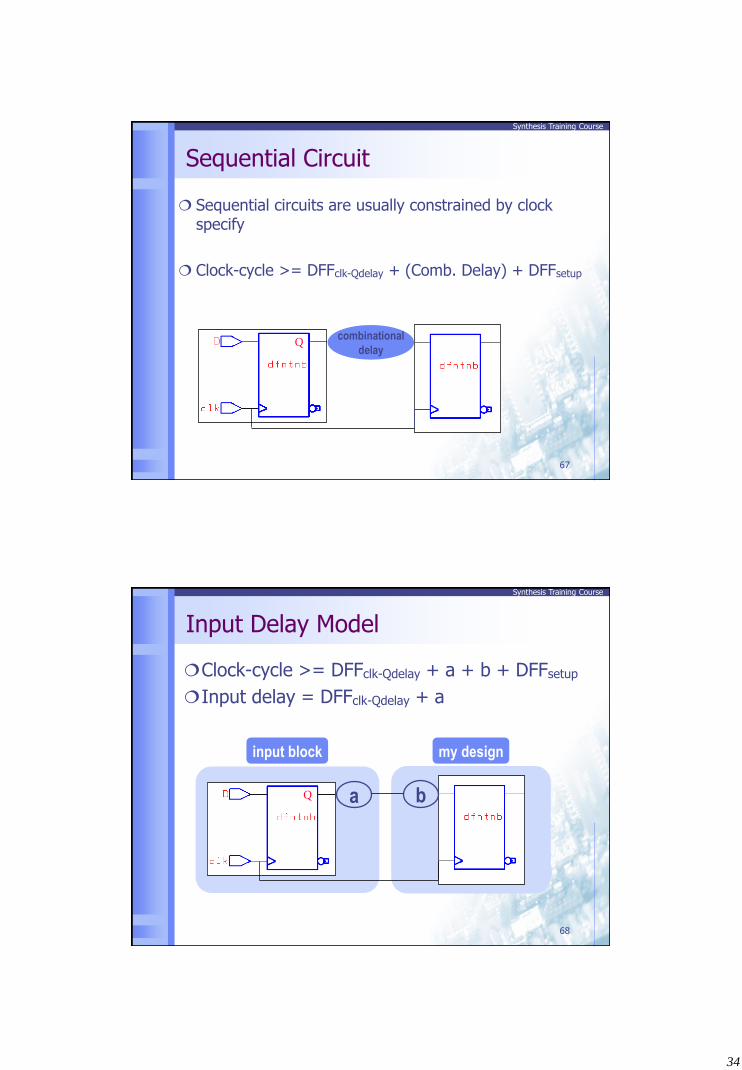
Sequential Circuit
Sequential circuits are usually constrained by clock specify
Clock-cycle >= DFFclk-Qdelay + (Comb. Delay) + DFFsetup
combinational
delay Q
67
Synthesis Training Course
Input Delay Model
Clock-cycle >= DFFclk-Qdelay + a + b + DFFsetup
Input delay = DFFclk-Qdelay + a
Q a b
input block my design
68
35
Synthesis Training Course
Output Delay Model
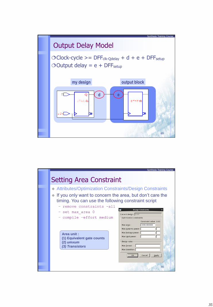
Clock-cycle >= DFFclk-Qdelay + d + e + DFFsetup
Output delay = e + DFFsetup
Q d e
output block my design
69
Synthesis Training Course
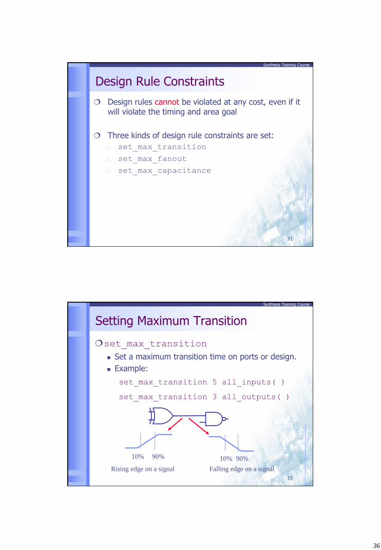
Setting Area Constraint Attributes/Optimization Constraints/Design Constraints
If you only want to concern the area, but don’t care the
timing. You can use the following constraint script – remove constraints –all
– set max_area 0
– compile –effort medium
Area unit :
(1) Equivalent gate counts
(2) umxum
(3) Transistors
70
36
Synthesis Training Course
Design Rule Constraints
Design rules cannot be violated at any cost, even if it will violate the timing and area goal
Three kinds of design rule constraints are set:
1. set_max_transition
2. set_max_fanout
3. set_max_capacitance
71
Synthesis Training Course
Setting Maximum Transition
set_max_transition
Set a maximum transition time on ports or design.
Example:
10% 10% 90% 90%
Rising edge on a signal Falling edge on a signal
set_max_transition 5 all_inputs( )
set_max_transition 3 all_outputs( )
72
37
Synthesis Training Course
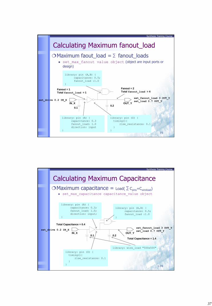
Calculating Maximum fanout_load
0.10.2
library: pin (A,B) {
capacitance: 0.5;
fanout_load :1.0
}
Fanout = 1
Total fanout_load = 1
set_fanout_load 3 OUT_Y
set_load 0.7 OUT_Yset_drive 0.2 IN_X
IN_X OUT_Y
library: pin (A) {
capacitance: 0.3
fanout_load: 1.0
direction: input
}
library: pin (Z) {
timing(){
rise_resistance: 0.1
}
}
Fanout = 2
Total fanout_load = 4
Maximum faout_load = fanout_loads set_max_fanout value object (object are input ports or
design)
73
Synthesis Training Course
1-74
Calculating Maximum Capacitance
0.1 0.2
library: pin (A) {
capacitance: 0.3;
fanout_load: 1.0;
direction: input;
}
library: pin (A,B) {
capacitance: 0.5;
fanout_load :1.0
}
library: wire_load "500x500"
Total Capacitance = 1.4
Total Capacitance = 0.4
set_fanout_load 3 OUT_Y
set_load 0.7 OUT_Yset_drive 0.2 IN_X
IN_X OUT_Y
library: pin (Z) {
timing(){
rise_resistance: 0.1
}
}
Maximum capacitance = Load( Cpins+Cwireload)
set_max_capacitance capacitance_value object
38
Synthesis Training Course
1-75
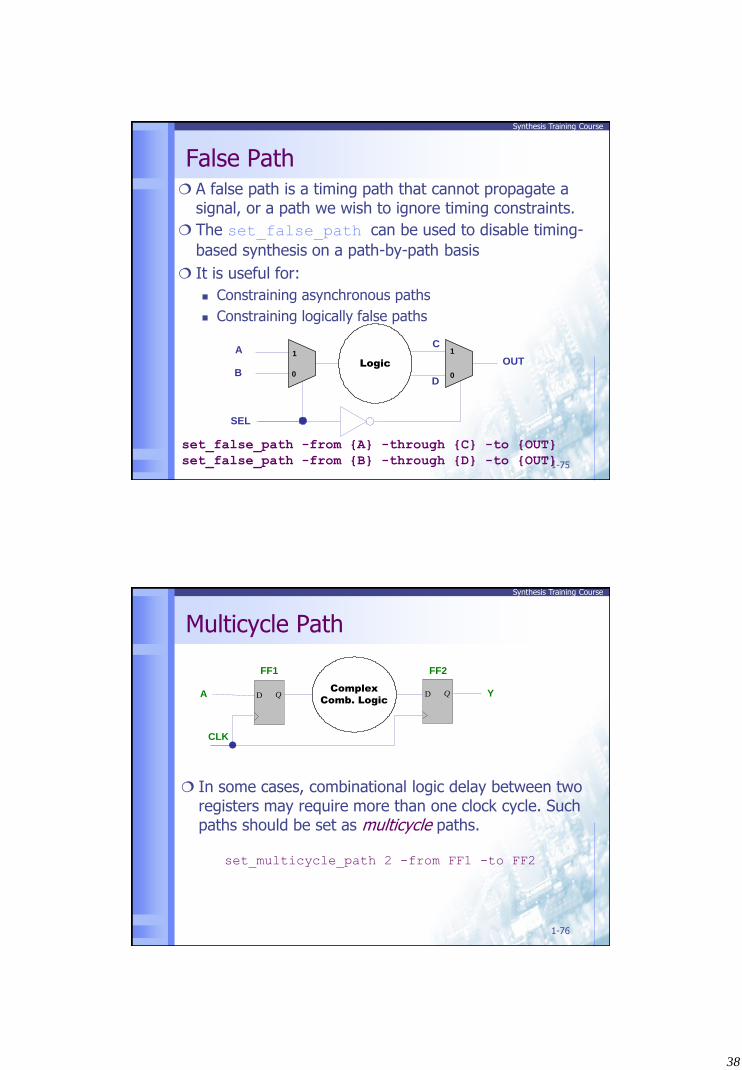
A false path is a timing path that cannot propagate a signal, or a path we wish to ignore timing constraints.
The set_false_path can be used to disable timing-
based synthesis on a path-by-path basis
It is useful for:
Constraining asynchronous paths
Constraining logically false paths
False Path
Logic
A
B
SEL
OUT1 1
00D
C
set_false_path -from {A} -through {C} -to {OUT}
set_false_path -from {B} -through {D} -to {OUT}
Synthesis Training Course
1-76
Multicycle Path
In some cases, combinational logic delay between two registers may require more than one clock cycle. Such paths should be set as multicycle paths.
Complex
Comb. LogicD Q D Q
FF1 FF2
CLK
A Y
set_multicycle_path 2 -from FF1 -to FF2
39
Synthesis Training Course
1-77
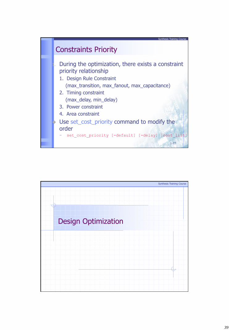
Constraints Priority
1. During the optimization, there exists a constraint priority relationship
1. Design Rule Constraint
(max_transition, max_fanout, max_capacitance)
2. Timing constraint
(max_delay, min_delay)
3. Power constraint
4. Area constraint
Use set_cost_priority command to modify the order – set_cost_priority [-default] [-delay] [cost_list]
Synthesis Training Course
Design Optimization
40
Synthesis Training Course
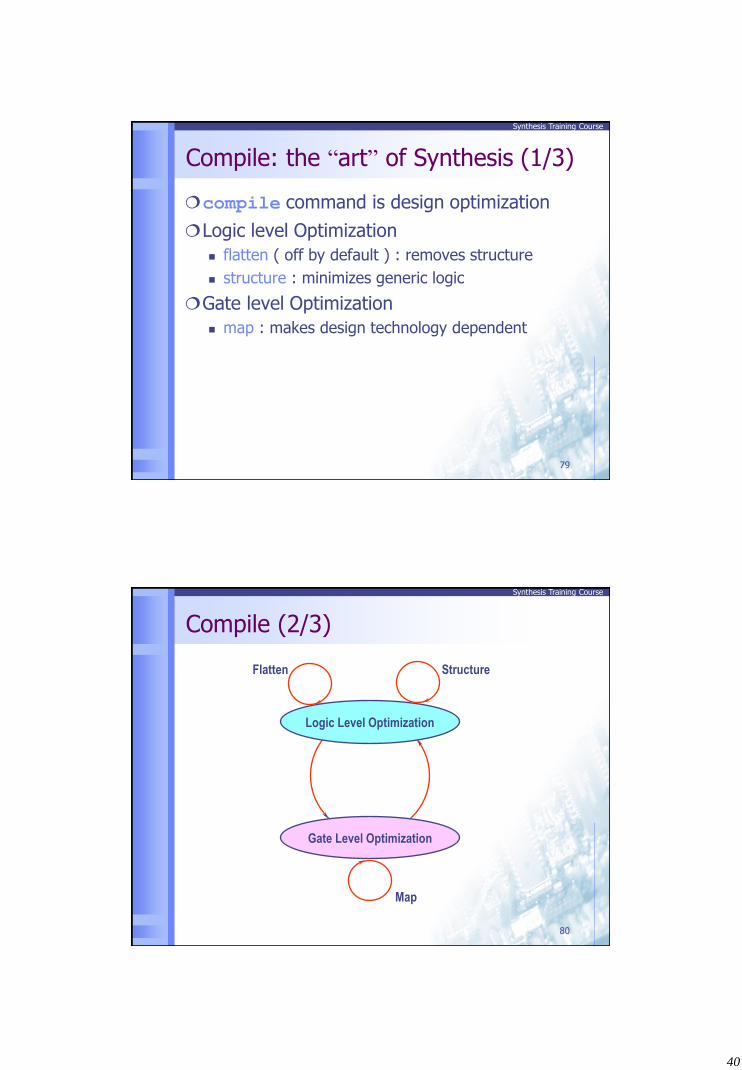
Compile: the “art” of Synthesis (1/3)
compile command is design optimization
Logic level Optimization
flatten ( off by default ) : removes structure
structure : minimizes generic logic
Gate level Optimization
map : makes design technology dependent
79
Synthesis Training Course
Compile (2/3)
Logic Level Optimization
Gate Level Optimization
Structure Flatten
Map
80
41
Synthesis Training Course
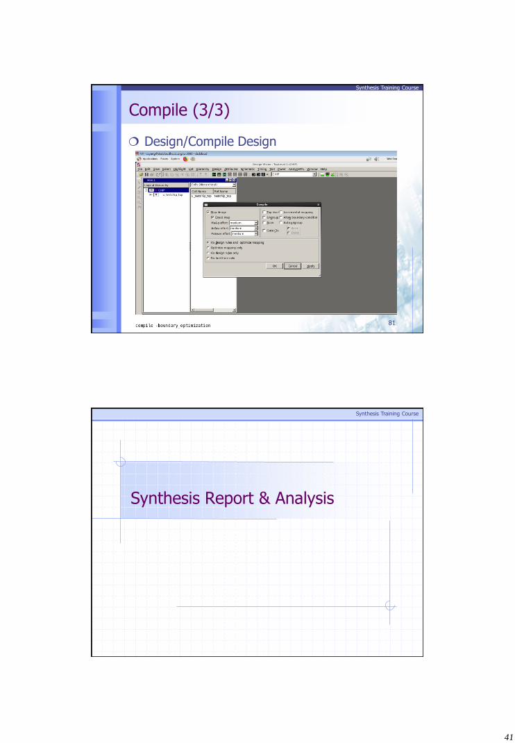
Compile (3/3)
Design/Compile Design
81
Synthesis Training Course
Synthesis Report & Analysis
42
Synthesis Training Course
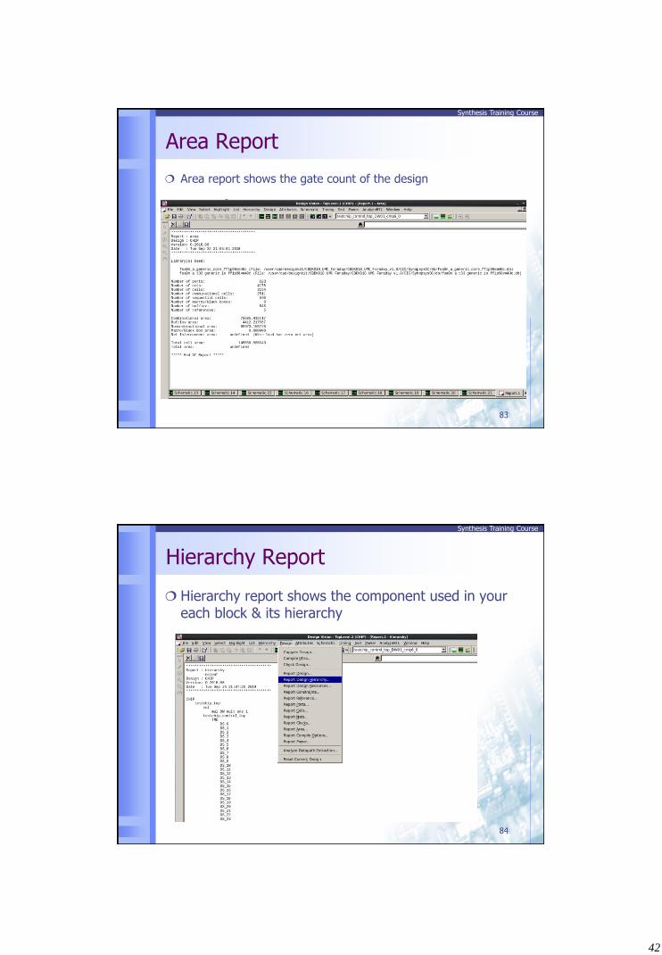
Area Report
Area report shows the gate count of the design
83
Synthesis Training Course
Hierarchy Report
Hierarchy report shows the component used in your each block & its hierarchy
84
43
Synthesis Training Course
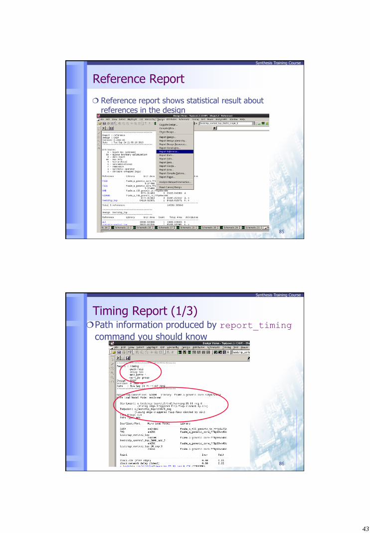
Reference Report
Reference report shows statistical result about references in the design
85
Synthesis Training Course
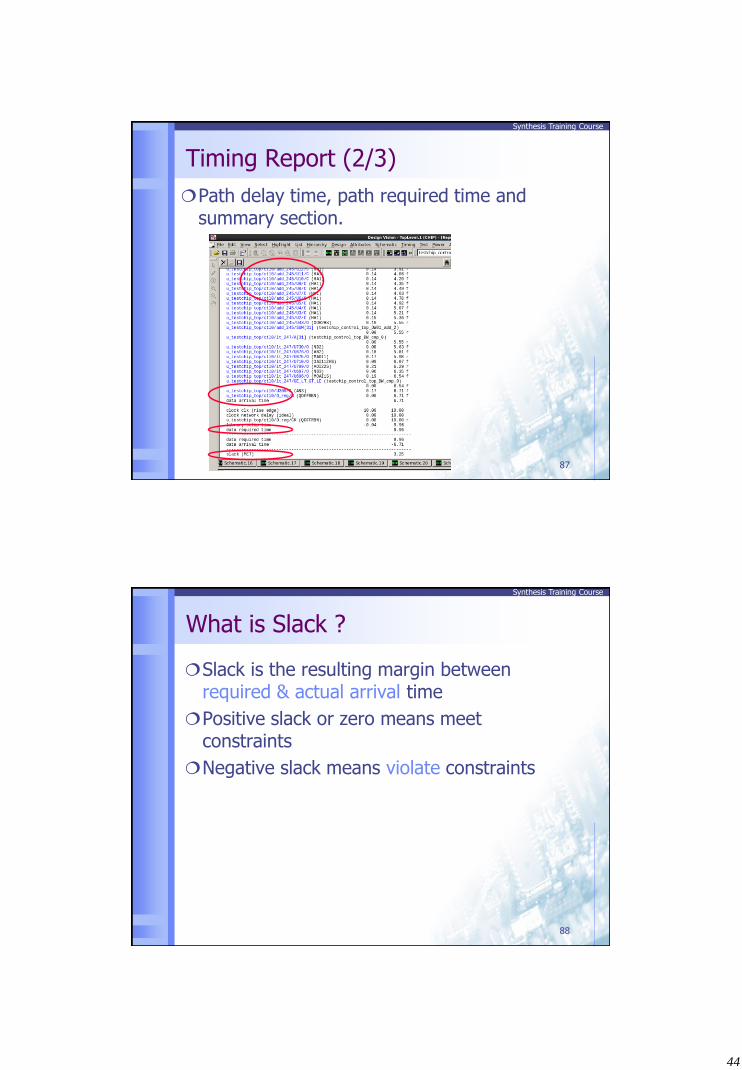
Timing Report (1/3) Path information produced by report_timing
command you should know
86
44
Synthesis Training Course
Timing Report (2/3)
Path delay time, path required time and summary section.
87
Synthesis Training Course
What is Slack ?
Slack is the resulting margin between required & actual arrival time
Positive slack or zero means meet constraints
Negative slack means violate constraints
88
45
Synthesis Training Course
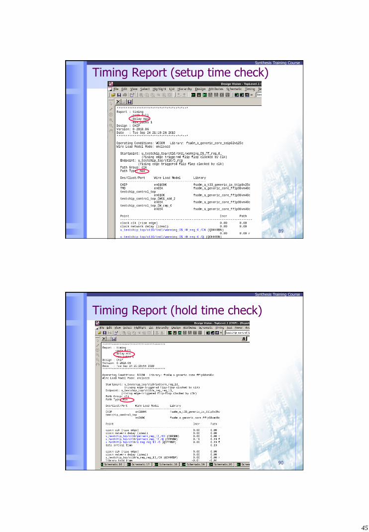
Timing Report (setup time check)
89
Synthesis Training Course
Timing Report (hold time check)
90
46
Synthesis Training Course
Outline
Introduction to Cell-based Design Flow
Logic Synthesis
Introduction to Logic Synthesis
Coding Style for Synthesis
Static Timing Analysis
Synopsys Design Compiler
SDF and Gate-Level Simulation
91
Synthesis Training Course
Standard Delay Format (SDF)
An SDF file is an ASCII text file that stores timing data generated by EDA tools.
EDA tools share the timing data in the SDF file to be assured of consistent, accurate, and up-to-date data.
The timing data in the SDF file is represented in a tool-independent way and can include:
Delays: module path, device, interconnect, and port
Timing checks: setup, hold, recovery, skew, width, and period
Timing Constraints: path and skew
Incremental and absolute delays
Conditional and unconditional module path delays and timing checks
Design, instance, instance type or library specific timing
Scaling, environment, technology, and user-defined parameters
SDF was a Cadence Verilog XL feature for timing annotation.
92
47
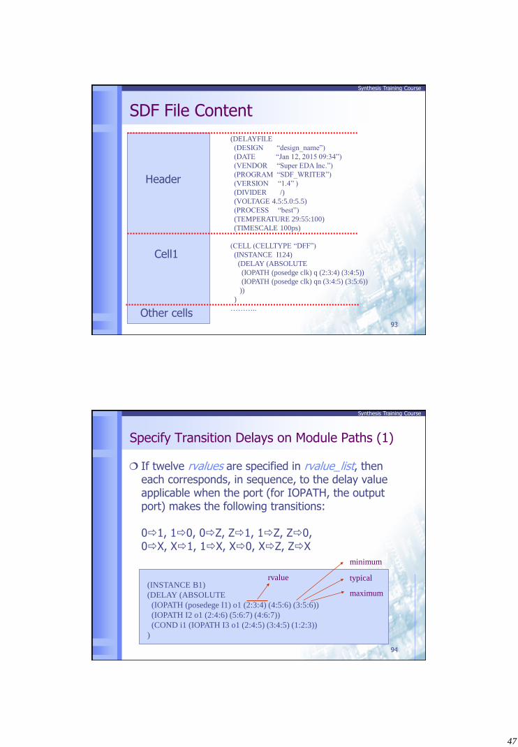
Synthesis Training Course
SDF File Content
(DELAYFILE
(DESIGN “design_name”)
(DATE “Jan 12, 2015 09:34”)
(VENDOR “Super EDA Inc.”)
(PROGRAM “SDF_WRITER”)
(VERSION “1.4” )
(DIVIDER /)
(VOLTAGE 4.5:5.0:5.5)
(PROCESS “best”)
(TEMPERATURE 29:55:100)
(TIMESCALE 100ps)
(CELL (CELLTYPE “DFF”)
(INSTANCE I124)
(DELAY (ABSOLUTE
(IOPATH (posedge clk) q (2:3:4) (3:4:5))
(IOPATH (posedge clk) qn (3:4:5) (3:5:6))
))
)
………..
Header
Cell1
Other cells 93
Synthesis Training Course
Specify Transition Delays on Module Paths (1)
If twelve rvalues are specified in rvalue_list, then each corresponds, in sequence, to the delay value applicable when the port (for IOPATH, the output port) makes the following transitions: 01, 10, 0Z, Z1, 1Z, Z0, 0X, X1, 1X, X0, XZ, ZX
(INSTANCE B1)
(DELAY (ABSOLUTE
(IOPATH (posedege I1) o1 (2:3:4) (4:5:6) (3:5:6))
(IOPATH I2 o1 (2:4:6) (5:6:7) (4:6:7))
(COND i1 (IOPATH I3 o1 (2:4:5) (3:4:5) (1:2:3))
)
minimum
typical
maximum
rvalue
94
48
Synthesis Training Course
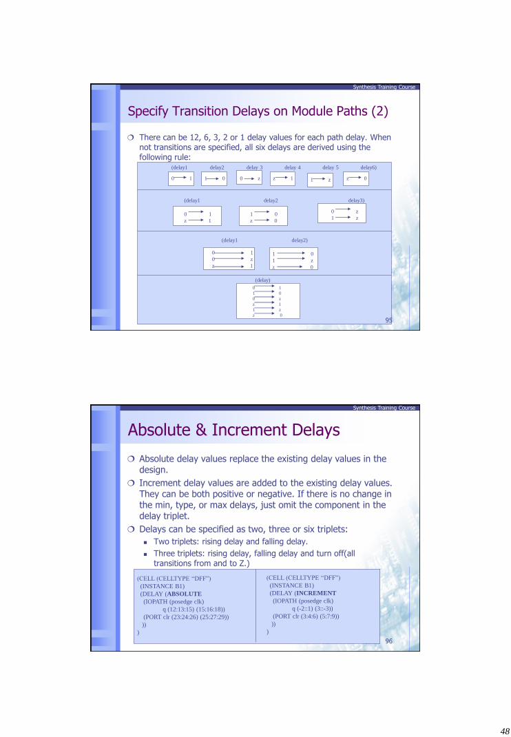
Specify Transition Delays on Module Paths (2)
There can be 12, 6, 3, 2 or 1 delay values for each path delay. When not transitions are specified, all six delays are derived using the following rule:
(delay1 delay2 delay 3 delay 4 delay 5 delay6)
1 0 0 z z 1 1 z z 0 0 1
(delay1 delay2 delay3)
0 1
z 1
1 0
z 0
0 z
1 z
(delay1 delay2)
1 0
1 z
z 0
0 1
0 z
z 1
(delay)
0 1
1 0
0 z
z 1
1 z
z 0
95
Synthesis Training Course
Absolute & Increment Delays
Absolute delay values replace the existing delay values in the design.
Increment delay values are added to the existing delay values. They can be both positive or negative. If there is no change in the min, type, or max delays, just omit the component in the delay triplet.
Delays can be specified as two, three or six triplets:
Two triplets: rising delay and falling delay.
Three triplets: rising delay, falling delay and turn off(all transitions from and to Z.)
Six triplets: rising, falling, 0 to z, z to 1, 1 to z and z to 0. (CELL (CELLTYPE “DFF”)
(INSTANCE B1)
(DELAY (ABSOLUTE
(IOPATH (posedge clk)
q (12:13:15) (15:16:18))
(PORT clr (23:24:26) (25:27:29))
))
)
(CELL (CELLTYPE “DFF”)
(INSTANCE B1)
(DELAY (INCREMENT
(IOPATH (posedge clk)
q (-2::1) (3::-3))
(PORT clr (3:4:6) (5:7:9))
))
)
96
49
Synthesis Training Course
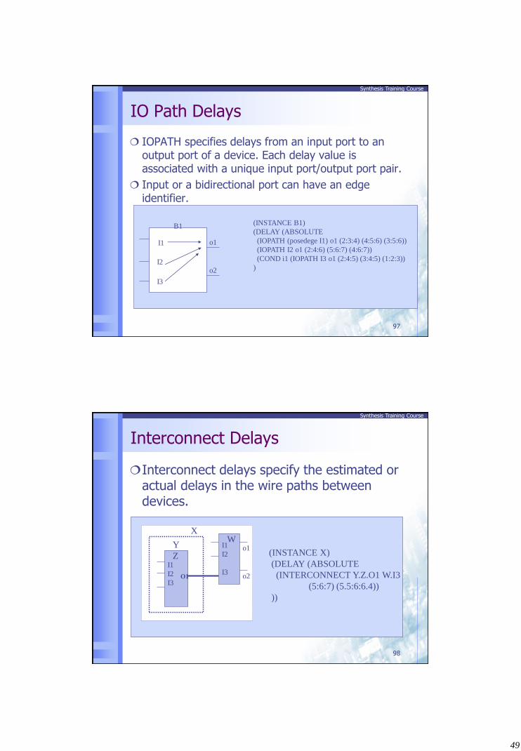
IO Path Delays
IOPATH specifies delays from an input port to an output port of a device. Each delay value is associated with a unique input port/output port pair.
Input or a bidirectional port can have an edge identifier.
B1
I1
I2
I3
o1
o2
(INSTANCE B1)
(DELAY (ABSOLUTE
(IOPATH (posedege I1) o1 (2:3:4) (4:5:6) (3:5:6))
(IOPATH I2 o1 (2:4:6) (5:6:7) (4:6:7))
(COND i1 (IOPATH I3 o1 (2:4:5) (3:4:5) (1:2:3))
)
97
Synthesis Training Course
Interconnect Delays
Interconnect delays specify the estimated or actual delays in the wire paths between devices.
X
Y W
Z I1
I2
I3 O1
I1
I2
I3
o1
o2
(INSTANCE X)
(DELAY (ABSOLUTE
(INTERCONNECT Y.Z.O1 W.I3
(5:6:7) (5.5:6:6.4))
))
98
50
Synthesis Training Course
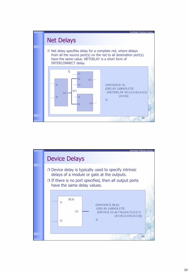
Net Delays
Net delay specifies delay for a complete net, where delays from all the source port(s) on the net to all destination port(s) have the same value. NETDELAY is a short form of INTERCONNECT delay.
I1
I2
O1
X I1
I2
I3
O1
I1
I2 O1
(INSTANCE X)
(DELAY (ABSOLUTE
(NETDELAY W1 (2:3:4) (3:4:5)
(4:5:6))
))
W1
99
Synthesis Training Course
100
Device Delays
Device delay is typically used to specify intrinsic delays of a module or gate at the outputs.
If there is no port specified, then all output ports have the same delay values.
I1
I2
O1
BLK
(INSTANCE BLK)
(DELAY (ABSOLUTE
(DEVICE O1 (6:7:8) (4:6:7) (5:6:7)
(4:5:8) (2:4:8) (4:5:8))
))
51
Synthesis Training Course
1-101
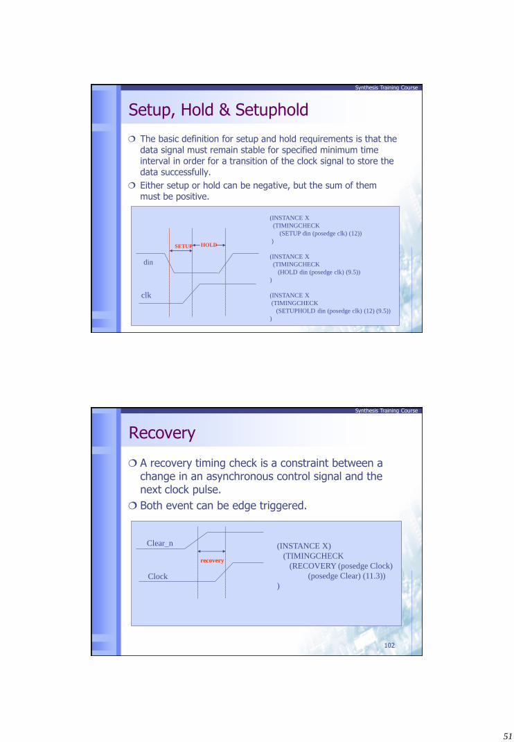
Setup, Hold & Setuphold
The basic definition for setup and hold requirements is that the data signal must remain stable for specified minimum time interval in order for a transition of the clock signal to store the data successfully.
Either setup or hold can be negative, but the sum of them must be positive.
HOLD SETUP
din
clk
(INSTANCE X
(TIMINGCHECK
(SETUP din (posedge clk) (12))
)
(INSTANCE X
(TIMINGCHECK
(HOLD din (posedge clk) (9.5))
)
(INSTANCE X
(TIMINGCHECK
(SETUPHOLD din (posedge clk) (12) (9.5))
)
Synthesis Training Course
Recovery
A recovery timing check is a constraint between a change in an asynchronous control signal and the next clock pulse.
Both event can be edge triggered.
recovery
Clear_n
Clock
(INSTANCE X)
(TIMINGCHECK
(RECOVERY (posedge Clock)
(posedge Clear) (11.3))
)
102
52
Synthesis Training Course
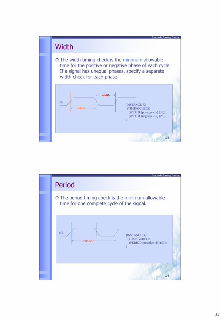
Width
The width timing check is the minimum allowable time for the positive or negative phase of each cycle. If a signal has unequal phases, specify a separate width check for each phase.
width
width
(INSTANCE X)
(TIMINGCHECK
(WIDTH (posedge clk) (30))
(WIDTH (negedge clk) (25))
)
clk
103
Synthesis Training Course
Period
The period timing check is the minimum allowable time for one complete cycle of the signal.
(INSTANCE X)
(TIMINGCHECK
(PERIOD (posedge clk) (50))
)
clk
Period
104
53
Synthesis Training Course
SDF Applications
SDF is the most commonly used format to exchange timing information from one EDA tools to another.
The most commonly used version of SDF is 2.1.
SDF was adopted by IEEE together with Verilog HDL from Open Verilog International (OVI).
SDF was created exclusively for Verilog to annotate timing to the specify blocks.
SDF is also widely used by other tools and HDL.
105
Synthesis Training Course
Verilog Gate-level Simulation
Add the following task in your test fixture for SDF annotation: initial begin
$sdf_annotate(“design.sdf”, instance_name_of_design);
end
Add cell library simulation model: Add the library simulation model file
-v /your_path/fsa0m_a_generic_core_21.lib.src –v
fsa0m_a_t33_generic_io_21.lib.src +access+r
106
54
Synthesis Training Course
Gate-Level Simulation (Verilog)
Write out gate-level netlist (two methods)
1. File/Save As Verilog (for File format)
2. design_vision> write -format verilog -hierarchy –output chip.vg
Get SDF (two methods)
1. File/Save Info Design timing Select chip.sdf
2. design_vision > write_sdf -version 2.1 -context verilog chip.sdf
Modifiy your testfixture file
$sdf_annotate("the_SDF_file_name",
the_top_level_module _instance_name);
For example: $sdf_annotate("chip.sdf", top);
Simulation using NC-Verilog
ncverilog chip.vg your_testfixture.v -v your_simulation_model.v +
access+r
107
Synthesis Training Course
108
Thank You For Your Attention!