miec* access device for 3d-crosspoint nonvolatile … access device for 3d-crosspoint nonvolatile...
TRANSCRIPT

© 2012 IBM Corporation
MIEC* Access Device for 3D-Crosspoint Nonvolatile Memory Arrays
IBM Almaden Research Center, San Jose, CA
* Mixed-Ionic-Electronic-Conduction

© 2012 IBM Corporation2
Storage Class Memory (SCM)
A new class of storage/memory devices that blurs the distinction between …
Memory (fast, expensive, volatile) and Storage (slow, cheap, nonvolatile)
• Solid-state no moving parts• Nonvolatile retains data on power-off• Fast access speed approaching DRAM• High endurance many program/erase cycles• Low cost per bit approaching hard disk
(Wilcke, USENIX FAST tutorial, 2009)
© 2012 IBM Corporation3
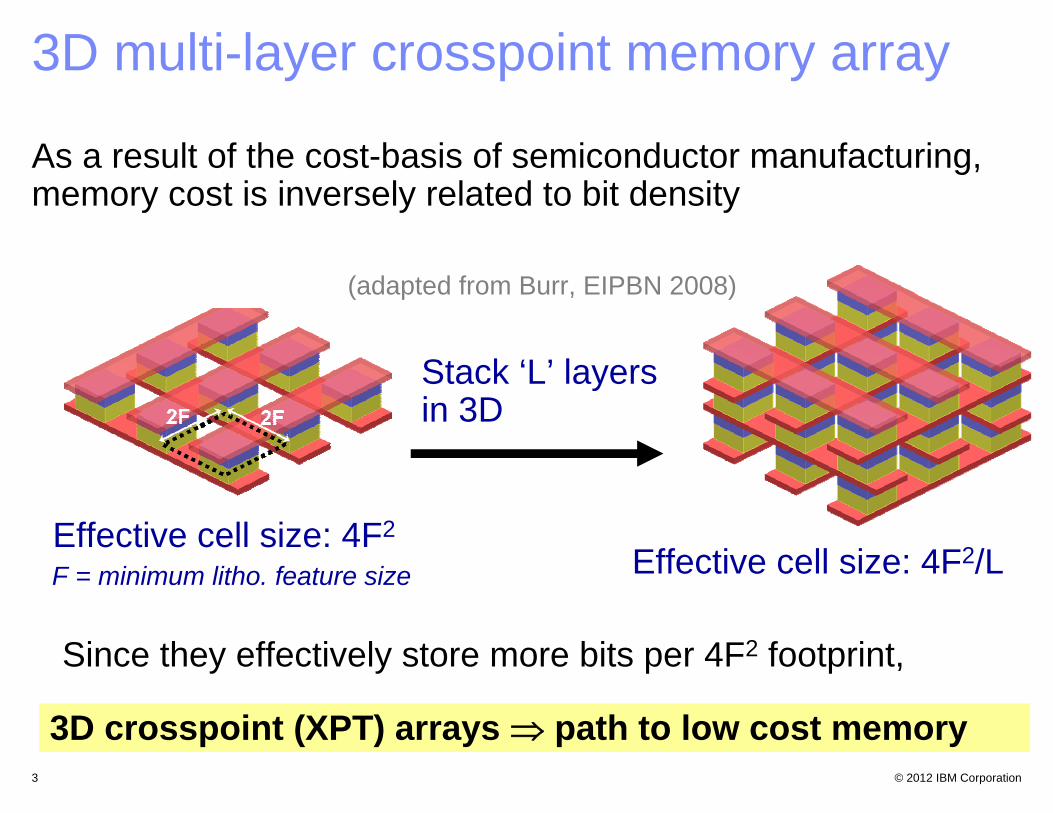
3D multi-layer crosspoint memory array
Effective cell size: 4F2Effective cell size: 4F2/L
Stack ‘L’ layers in 3D
F = minimum litho. feature size
As a result of the cost-basis of semiconductor manufacturing, memory cost is inversely related to bit density
Since they effectively store more bits per 4F2 footprint,
3D crosspoint (XPT) arrays path to low cost memory
(adapted from Burr, EIPBN 2008)

© 2012 IBM Corporation4
Nonvolatile Memory (NVM) candidates
• NAND Flash- very dense ( low bit cost) - currently at sub-20nm, but- endurance/retention get worse as scaling limits approached
• Phase Change Memory (PCM)
• Magnetic RAM (MRAM)- Spin-Torque-Transfer (STTRAM) arrays- Racetrack
• Resistive RAM (RRAM)- Oxide-based, or- Solid-electrolyte Conductive-Bridge RAM
Several NVM technology options for SCM

© 2012 IBM Corporation5
Phase Change Memory (PCM)Top Electrode (TE)
Bottom Electrode(BE)
Dielectric
crystalline amorphous
Top Electrode (TE)crystalline
RESET stateHigh Resistance
SET stateLow Resistance
SET (heat to crystallize)
RESET (melt + quench)(Burr et al, JVST B 2010)
• Mature (for emerging NVM)• Multiple-Level Cell capable• Scalable• Resistance drift• High reset current (density)
~10 MA/cm2 needed even for scaled PCM

© 2012 IBM Corporation6
Resistive RAM (RRAM)
RESET
“Forming”step
SET
Top electrode
Bot. electrode
insulator
Conductivefilament
(Burr: CMOS ET 2011)
V and I-driven creation & removal of conducting regions in insulator
Low resistance High resistance
RRAM examples
• Simple cell structure, usually fab-friendly• Low programming current (~10-100uA)• Good high temperature retention• High speed switching (sub-ns shown)• High endurance• Less mature (limited large array studies)• Intra- and inter-device variability
• TiN / HfOx/TiOx / TiN
H.Y. Lee et al, IEDM 2008, 2009, 2010 (ITRI)
• Pt / TaOx/ Pt
Z. Wei et al, IEDM 2008 (Panasonic)
Based on O-vacancy motion
Based on metal ion motion
• W / AgGeS / Ag
M.N. Kozicki et al, NVMTS 2005 (Arizona State Univ.)
The best RRAM candidates require bipolar operation
Typically, the best RRAM devices have SET and RESET voltages of opposite polarity
© 2012 IBM Corporation7
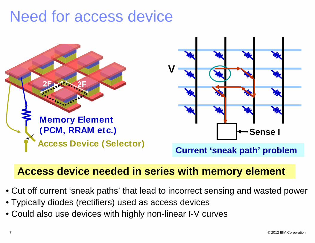
Need for access device
Memory Element (PCM, RRAM etc.)Access Device (Selector)
V
Sense I
Current ‘sneak path’ problem
Access device needed in series with memory element
• Cut off current ‘sneak paths’ that lead to incorrect sensing and wasted power• Typically diodes (rectifiers) used as access devices• Could also use devices with highly non-linear I-V curves
© 2012 IBM Corporation8
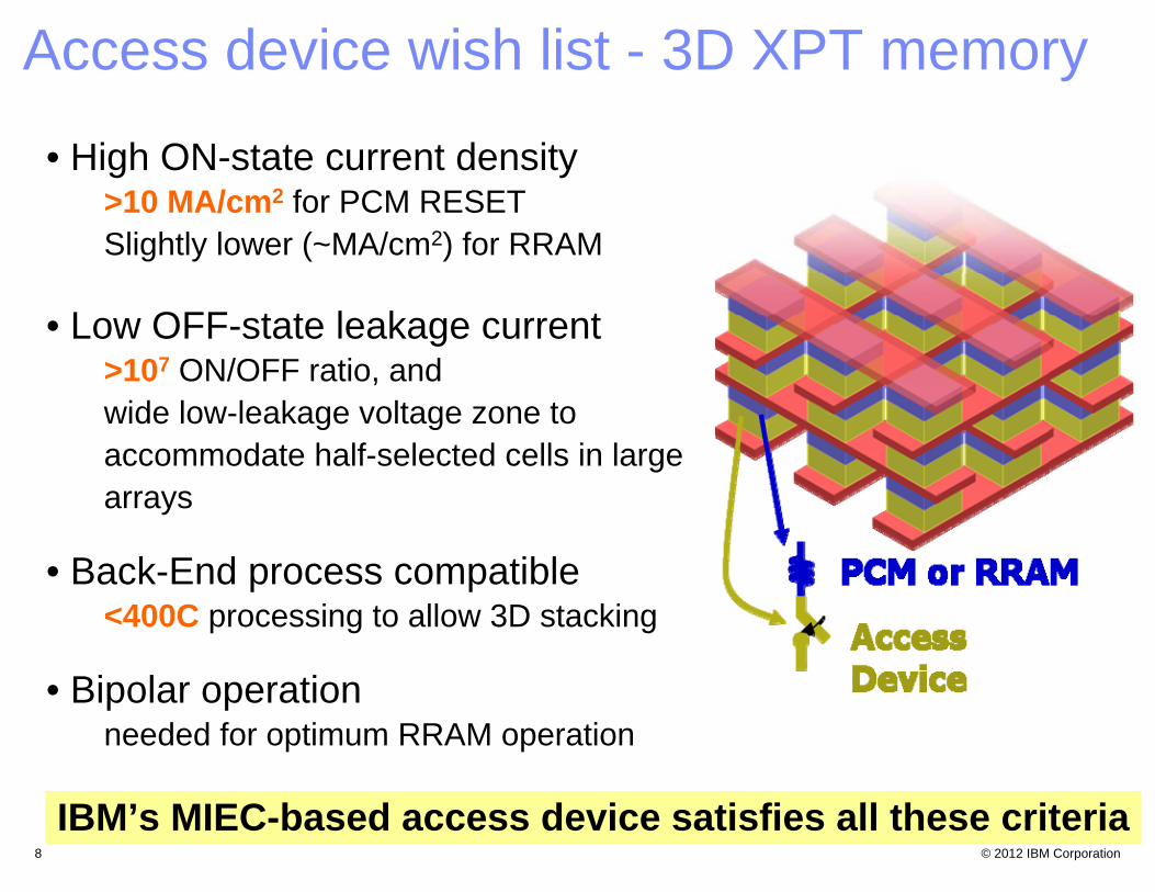
Access device wish list - 3D XPT memory
• High ON-state current density>10 MA/cm2 for PCM RESETSlightly lower (~MA/cm2) for RRAM
• Low OFF-state leakage current>107 ON/OFF ratio, andwide low-leakage voltage zone to accommodate half-selected cells in large arrays
• Back-End process compatible<400C processing to allow 3D stacking
• Bipolar operationneeded for optimum RRAM operation
IBM’s MIEC-based access device satisfies all these criteria

© 2012 IBM Corporation9
• Basic characteristics
• Switching speed
• Cycling endurance
• Scalability
© 2012 IBM Corporation10
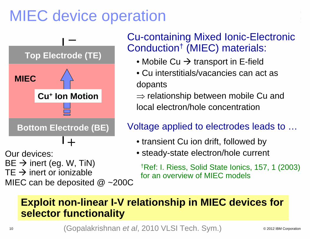
MIEC device operation
Bottom Electrode (BE)
Top Electrode (TE)
MIEC
Cu+ Ion Motion
Cu-containing Mixed Ionic-Electronic Conduction† (MIEC) materials:
• Mobile Cu transport in E-field• Cu interstitials/vacancies can act as dopants relationship between mobile Cu and local electron/hole concentration
Voltage applied to electrodes leads to …• transient Cu ion drift, followed by• steady-state electron/hole currentOur devices:
BE inert (eg. W, TiN)TE inert or ionizableMIEC can be deposited @ ~200C
Exploit non-linear I-V relationship in MIEC devices for selector functionality
(Gopalakrishnan et al, 2010 VLSI Tech. Sym.)
†Ref: I. Riess, Solid State Ionics, 157, 1 (2003) for an overview of MIEC models

© 2012 IBM Corporation11
Wide-area TEC device – DC sweeps
10A
1A
100nA
10nA
1nA
100pA
10pA
|Cur
rent
|
-0.6 -0.4 -0.2 0 0.2 0.30.1-0.1-0.3-0.5Applied TEC voltage [V]
VB(-0.355V)
VA(0.255V)
Voltage margin|VB| + VA
(0.61V)
~80 nm BEC ionizable TEC
Exponential DC I-V curve for negative TEC bias
(Gopalakrishnan et al, 2010 VLSI Tech. Sym.)
© 2012 IBM Corporation12
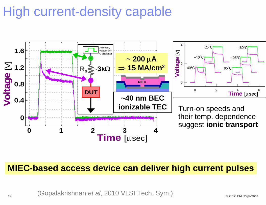
High current-density capableVo
ltage
[V]
0 1 2Time [sec]
0
0.4
0.8
1.2
1.6
~3k
ArbitraryWaveformGenerator
DUT
Rs
3 4
~40 nm BEC ionizable TEC
~ 200 A 15 MA/cm2
Time [sec]
Volta
ge [V
]
Time [sec]
Volta
ge [V
]
Turn-on speeds and their temp. dependence suggest ionic transport
MIEC-based access device can deliver high current pulses
(Gopalakrishnan et al, 2010 VLSI Tech. Sym.)

© 2012 IBM Corporation13
Bipolar I-V curves100A
1A
100nA
10nA
1nA
100pA
10pA
0.30.1-0.1-0.3-0.5
|Cur
rent
|
AppliedVoltage
[V]1pA
10A
0.5
W
gapoverlap
W
gapoverlap
W=200nmGap=100nmOverlap=250nm
200nminert TEC
80nm BEC
10A
1A
100nA
10nA
1nA
100pA
10pA
1pA
100A
|Cur
rent
|
-1 -0.8 -0.6 -0.4 -0.2 0 0.2 0.4 0.6 0.8
Voltage [V]
MIEC
TEC
ILDBEC
poly-Si series resistor
MIEC
TEC
ILDBEC
poly-Si series resistor
Lateral (bridge) device Vertical device with scaled TEC
• Similar TEC and BEC areas, along with reduced MIEC volume eliminates abrupt ‘filamentary’ switching symmetric I-V curves
• Suitable (desirable) for bipolar memory elements such as RRAM
MIEC access devices can operate in both polarities
(Gopalakrishnan et al, 2010 VLSI Tech. Sym.)

© 2012 IBM Corporation14
Integration into 200 mm wafer process
As-deposited
Post-CMP
TEM x-section
180 nm CMOS Front-End 1T1S
(1 transistor + 1 selector)
CMP process for MIEC material with modified commercial Cu slurry
self-aligned MIEC Diode-in-Via (DIV) in a 200 mm process(Shenoy et al, 2011 VLSI Tech. Sym.)
© 2012 IBM Corporation15
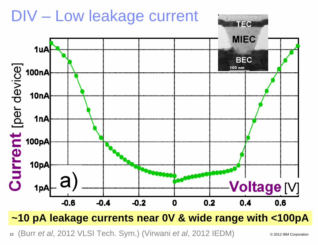
DIV – Low leakage current
~10 pA leakage currents near 0V & wide range with <100pA(Burr et al, 2012 VLSI Tech. Sym.) (Virwani et al, 2012 IEDM)

© 2012 IBM Corporation16
DIV – High current capable
Scope
Pulsegenerator
V
t
Current
t50
100’s of uA pulse currents ON/OFF ratio >107
(Shenoy et al, 2011 VLSI Tech. Sym.)
© 2012 IBM Corporation17
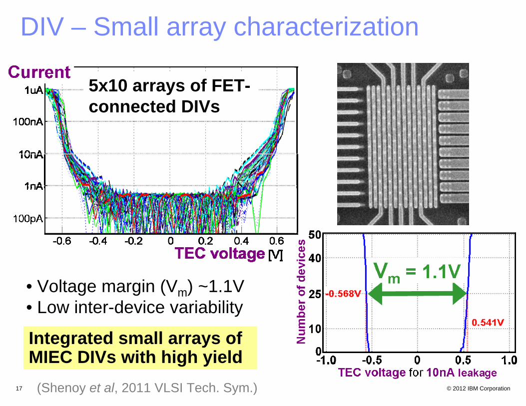
DIV – Small array characterization
5x10 arrays of FET-connected DIVs
• Voltage margin (Vm) ~1.1V • Low inter-device variability
Integrated small arrays of MIEC DIVs with high yield
(Shenoy et al, 2011 VLSI Tech. Sym.)
© 2012 IBM Corporation18
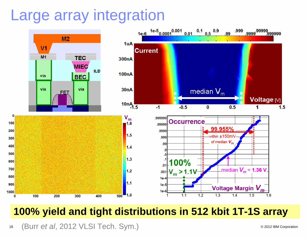
Large array integration
100% yield and tight distributions in 512 kbit 1T-1S array(Burr et al, 2012 VLSI Tech. Sym.)
© 2012 IBM Corporation19
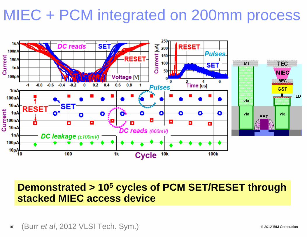
MIEC + PCM integrated on 200mm process
Demonstrated > 105 cycles of PCM SET/RESET through stacked MIEC access device
(Burr et al, 2012 VLSI Tech. Sym.)

© 2012 IBM Corporation20
• Basic characteristics
• Switching speed
• Cycling endurance
• Scalability

© 2012 IBM Corporation21
Switching speed at high currents (WRITE)
MIEC access device can supply >150uA in 15ns …… sufficient to RESET PCM
(Virwani et al, IEDM 2012)
0
100
200
300
400
500
Time
Current[uA]
5 ns/division15ns
a)Increasing pulseamplitude
RESET current [uA]100 150 200 300 400
30nA
100nA
300nA
1uA
Rea
d C
urre
nt@
660m
V
post-SET
RESETPost-
© 2012 IBM Corporation22
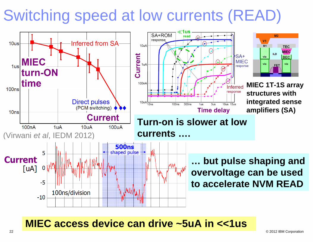
Switching speed at low currents (READ)
MIEC access device can drive ~5uA in <<1us
(Virwani et al, IEDM 2012)
MIEC 1T-1S array structures with integrated sense amplifiers (SA)
Turn-on is slower at low currents ….
… but pulse shaping and overvoltage can be used to accelerate NVM READ

© 2012 IBM Corporation23
• Basic characteristics
• Switching speed
• Cycling endurance
• Scalability

© 2012 IBM Corporation24
Cycling endurance – low current
OFF current at -0.2V100pA
1nA
10nA
100nA
1A
10A
100A
|Cur
rent
|
ON current >5Asufficient for PCM-read
(Rs~30k Vapplied~ -0.8V)
OFF current at -0.3V
Pulse duration ~2s
100 1000 104 105 106 108 109 1010107
Pulses
80 nm BEC Wide-area ionizable TEC
Testing time-limited!
Low current (memory READ) endurance > 1010 cycles
(Gopalakrishnan et al, 2010 VLSI Tech. Sym.)

© 2012 IBM Corporation25
Cycling endurance – high current
DC I-V curves monitored in between 100uA pulses
Leakage current rises …
… and voltage margin shrinks
After many cycles …
Finite high current (memory WRITE) endurance
(Shenoy et al, 2011 VLSI Tech. Sym.)
© 2012 IBM Corporation26
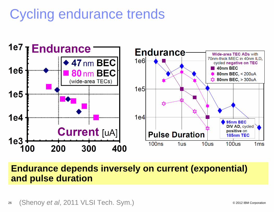
Cycling endurance trends
Endurance depends inversely on current (exponential) and pulse duration
(Shenoy et al, 2011 VLSI Tech. Sym.)

© 2012 IBM Corporation27
Cycling endurance trends (continued)
>108 endurance for sub-45 nm-node PCM!( IRESET < 150 A )
Strong current-dependence of MIEC access device endurance persists across many different device structures
Expect even higher MIEC endurance for RRAM (IPROG/ERASE <100uA)
(Shenoy et al, 2011 VLSI Tech. Sym.)
© 2012 IBM Corporation28
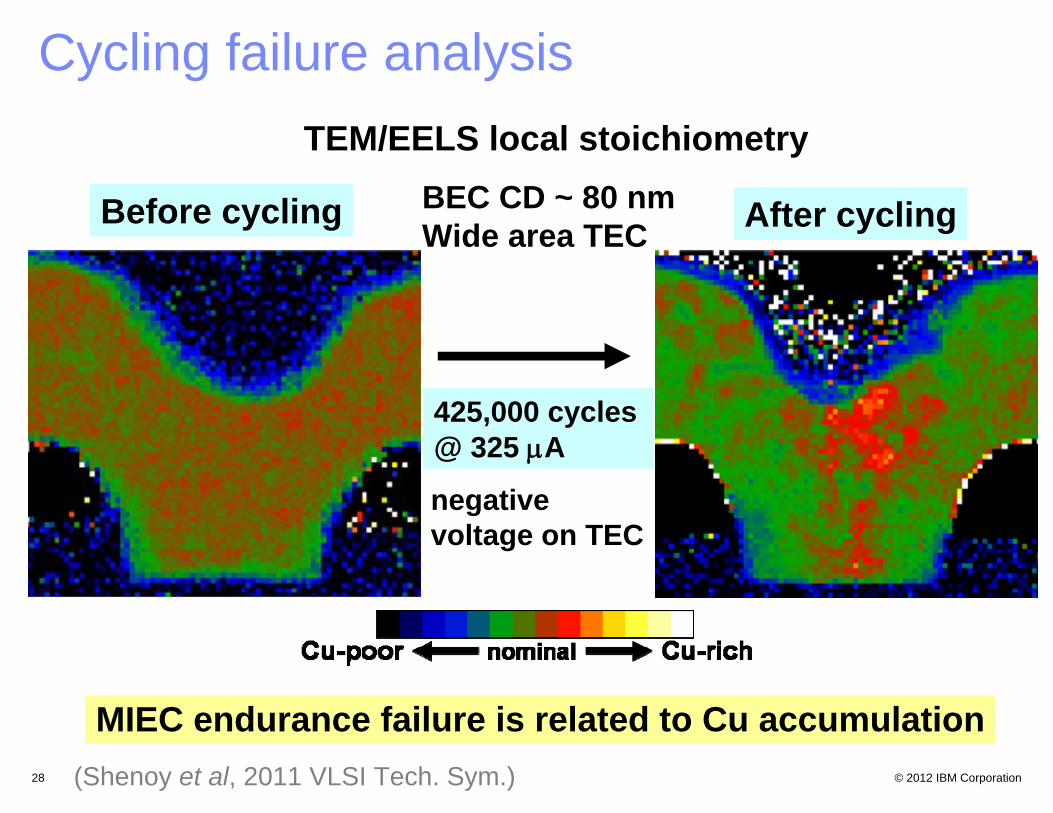
Cycling failure analysis
Before cycling After cycling
425,000 cycles @ 325 A
TEM/EELS local stoichiometryBEC CD ~ 80 nmWide area TEC
negative voltage on TEC
MIEC endurance failure is related to Cu accumulation(Shenoy et al, 2011 VLSI Tech. Sym.)

© 2012 IBM Corporation29
Cycling failure recovery
Endurance failure correctable by annealing and/or voltage pulses
(Shenoy et al, 2011 VLSI Tech. Sym.)

© 2012 IBM Corporation30
• Basic characteristics
• Switching speed
• Cycling endurance
• Scalability

© 2012 IBM Corporation31
Conductive AFM device characterization
Large thermal process budget window Manufacturable deposition
Process optimization for higher Vm
Rapid learning cycles enabled by cAFM
(Burr et al, 2012 VLSI Tech. Sym.)
Short loop process flows on relevant structures

© 2012 IBM Corporation32
Lateral scaling – BEC size
80nm40nm
1m10A
1A
100nA
10nA
1nA
100pA
|Cur
rent
|
10pA
Vbias-0.50V
-0.35V
-0.30V
-0.25V
Via height:20nm
200 400 600 800
Time [ns]0
0
0.4
0.8
1.2
1.6
Volta
ge [V
]
1000 104 105 106Via height: 40nm
250nm
Via area = CD2 [nm2]
Wide-area Ionizable TEC
19 nm
Current scales well with BEC size over several orders of magnitude
Suggests non-filamentary nature of operation mechanism(Gopalakrishnan et al, 2010 VLSI Tech. Sym.)
© 2012 IBM Corporation33
Selector functionality is maintained in fully confined MIEC devices with reduced TEC and BEC size
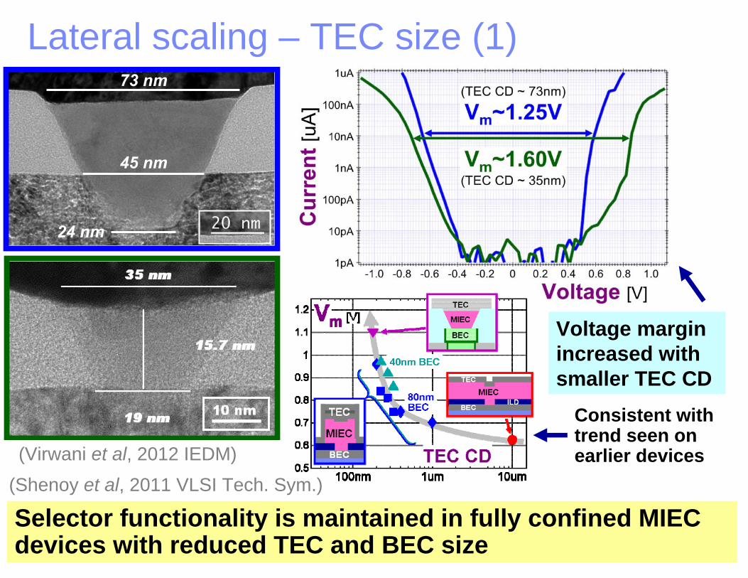
Lateral scaling – TEC size (1)
Voltage margin increased with smaller TEC CD
(Virwani et al, 2012 IEDM)(Shenoy et al, 2011 VLSI Tech. Sym.)
Consistent with trend seen on earlier devices

© 2012 IBM Corporation34
Ultra-scaled MIEC access devices can still deliver >100uA pulse currents in both polarities
Lateral scaling – TEC size (2)
(Virwani et al, 2012 IEDM)

© 2012 IBM Corporation35
No lower limit to lateral scaling has been found so far
Lateral scaling – TEC size (3)
(Virwani et al, 2012 IEDM)
Sub-30nm lateral CD MIEC device

© 2012 IBM Corporation36
Thickness scaling trends
SiN
Si wafer
BECoxide
C-AFMtip
TEC
MIEC dmin
Cumulative distribution plots of 10nA MIEC voltage margin
MIEC devices are well behaved down to 12nm minimum inter-electrode distance (dmin)
(Virwani et al, 2012 IEDM)
© 2012 IBM Corporation37
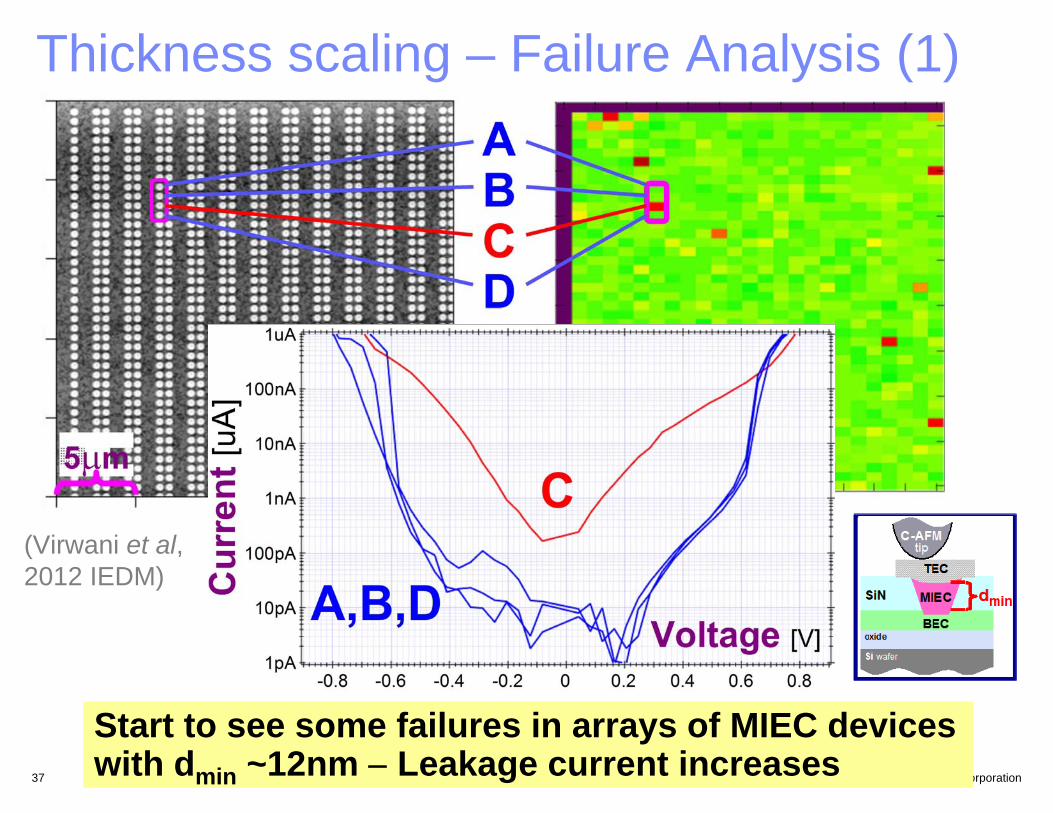
Thickness scaling – Failure Analysis (1)
Start to see some failures in arrays of MIEC devices with dmin ~12nm Leakage current increases
(Virwani et al, 2012 IEDM)

© 2012 IBM Corporation38
Thickness scaling – Failure Analysis (2)
Lower limit seen for thickness scaling of this MIEC access device
(Virwani et al, 2012 IEDM)Good
Good
Bad
Use TEM to correlate device failures to MIEC thickness

© 2012 IBM Corporation39
Summary Symmetric MIEC access devices with “bipolar” device characteristics are uniquely
suitable for crosspoint RRAM, yet have sufficient current for PCM as well ... versatile selector for non-volatile memory arrays
MIEC devices can be deposited and processed at BEOL temperatures (and also survive 500C process) ...suitable for 3D multilayer stacking
MIEC device functionality demonstrated down to sub-30 nm CD, and voltage margin is preserved down to at ~11 nm thickness ...scalable
Ultra high current density obtained in pulsed mode for MIEC devices > 50 MA/cm2 @ 20 nm CD – ample current to drive either RRAM or PCM.
MIEC devices have very low leakage ~10pA near 0V …ON/OFF ratio > 107
Turn-on speed ~15ns at WRITE-level (150uA) current and <<1us at READ-level current (5uA) … high speed operation
MIEC device cycling endurance > 108 cycles shown @ sub 150 A current. Endurance improves exponentially at lower currents … high endurance
MIEC process demonstrated with 100% yields and low variability on 0.5 Mbit array ... bodes well for manufacturability

© 2012 IBM Corporation40
Acknowledgements – Team members
IBM AlmadenGeoffrey Burr, Rohit Shenoy, Kumar Virwani, Alvaro Padilla, Andrew Kellock, Charles Rettner, Donald Bethune, Robert Shelby, Khanh Nguyen, Amy Bowers, Mark Jurich, Robin King, Dean Pearson, Noel Arellano, Alexander FrizTEM Group: Philip Rice, Teya Topuria, Leslie Krupp, Eugene Delenia
IBM YorktownKailash Gopalakrishnan, Gloria Ho, Matthew BrightSky, Eric Joseph, Michael Lofaro, Simone Raoux, Jing Li, Ravi Dasaka
IBM India (SRDC: Semiconductor Research Development Center)Karthik Venkataraman, Rajan Pandey, Kota Murali
Management SupportBulent Kurdi, Chung Lam, Winfried Wilcke, Chandrasekhar Narayan, Tze-Chiang Chen
IBM Yorktown MRL Fabrication Line support
© 2012 IBM Corporation41
References
K. Virwani, G. W. Burr, R. S. Shenoy, C. T. Rettner, A. Padilla, T. Topuria, P. M. Rice, G. Ho, R. S. King, K. Nguyen, A. N. Bowers, M. Jurich, M. BrightSky, E. A. Joseph, A. J. Kellock, N. Arellano, B. N. Kurdi and K. Gopalakrishnan, "Sub-30nm scaling and high-speed operation of fully-confined Access-Devices for 3D crosspoint memory based on Mixed-Ionic-Electronic-Conduction (MIEC) Materials," 2012 IEEE International Electron Devices Meeting (IEDM 2012), T2.7, Dec 2012.
G. W. Burr, K. Virwani, R. S. Shenoy, A. Padilla, M. BrightSky, E. A. Joseph, M. Lofaro, A. J. Kellock, R. S. King, K. Nguyen, A. N. Bowers, M. Jurich, C. T. Rettner, B. Jackson, D. S. Bethune, R. M. Shelby, T. Topuria, N. Arellano, P. M. Rice, B. N. Kurdi, and K. Gopalakrishnan, "Large-scale (512kbit) integration of Multilayer-ready Access-Devices based on Mixed-Ionic-Electronic-Conduction (MIEC) at 100% yield," 2012 Symposium on VLSI Technology, T5-4, June 2012.
R. S. Shenoy, K. Gopalakrishnan, B. Jackson, K. Virwani, G. W. Burr, C. T. Rettner, A. Padilla, D. S. Bethune, R. M. Shelby, A. J. Kellock, M. Breitwisch, E. A. Joseph, R. Dasaka, R. S. King, K. Nguyen, A. N. Bowers, M. Jurich, A. M. Friz, T. Topuria, P. M. Rice, and B. N. Kurdi, "Endurance and Scaling Trends of Novel Access-Devices for Multi-Layer Crosspoint-Memory based on Mixed-Ionic-Electronic-Conduction (MIEC) Materials," 2011 Symposium on VLSI Technology, T5B-1, June 2011.
G. W. Burr, "Storage Class Memory," 2011 CMOS Emerging Technologies, June 2011.
K. Gopalakrishnan, R. S. Shenoy, C. T. Rettner, K. Virwani, D. S. Bethune, R. M. Shelby, G. W. Burr, A. J. Kellock, R. S. King, K. Nguyen, A. N. Bowers, M. Jurich, B. Jackson, A. M. Friz, T. Topuria, P. M. Rice, and B. N. Kurdi, "Highly-Scalable Novel Access Device based on Mixed Ionic Electronic Conduction (MIEC) Materials for High Density Phase Change Memory (PCM) Arrays," 2010 Symposium on VLSI Technology, 19.4, June 2010.
G. W. Burr, M. J. Breitwisch, M. Franceschini, D. Garetto, K. Gopalakrishnan, B. Jackson, B. Kurdi, C. Lam, L. A. Lastras, A. Padilla, B. Rajendran, S. Raoux, and R. Shenoy, “Phase change memory technology," Journal of Vacuum Science & Technology B, 28(2), 223-262 (2010).
Richard Freitas, Winfried Wilcke, Bülent Kurdi, and Geoffrey Burr, “Storage Class Memory, Technology, and Uses,” Tutorial T3, 7th USENIX Conference on File and Storage Technologies (FAST’09), February 2009.
G. W. Burr, K. Gopalakrishnan, R. S. Shenoy, C. T. Rettner, and B. N. Kurdi, “Storage Class Memory,” EIPBN 2008 --- The 52nd International Conference on Electron, Ion, and Photon Beam Technology and Nanofabrication, May 2008.