ml610429 - ラピスセミコンダクタ 8-bit microcontroller with a built-in lcd driver 1/29...
TRANSCRIPT
FEDL610429-05 Issue Date: Apr.24, 2015
ML610429 8-bit Microcontroller with a Built-in LCD driver
1/29
GENERAL DESCRIPTION
This LSI is a high-performance 8-bit CMOS microcontroller into which rich peripheral circuits, such as synchronous serial port, UART, I2C bus interface (master), melody driver, battery level detect circuit, RC oscillation type A/D converter, and LCD driver, are incorporated around 8-bit CPU nX-U8/100. The CPU nX-U8/100 is capable of efficient instruction execution in 1-instruction 1-clock mode by 3-stage pipe line architecture parallel processing. The Mask ROM is installed and is most suitable for battery-driven applications.
FEATURES
• CPU− 8-bit RISC CPU (CPU name: nX-U8/100)− Instruction system: 16-bit instructions− Instruction set: Transfer, arithmetic operations, comparison, logic operations, multiplication/division, bit
manipulations, bit logic operations, jump, conditional jump, call return stack manipulations, arithmetic shift, and so on
− Minimum instruction execution time 30.5 µs (@32.768 kHz system clock) 0.24 4µs (@4.096 MHz system clock)
• Internal memory− Internal 48KByte Mask ROM (24K×16 bits) (including unusable 1KByte TEST area)− Internal 3KByte Data RAM (3072×8 bits), 1KByte Display Allocation RAM (1024 x 8bit)− Internal 192-byte RAM for display
• Interrupt controller− 2 non-maskable interrupt sources (Internal source: 1, External source: 1)− 27 maskable interrupt sources (Internal sources: 19, External sources: 8)
• Time base counter− Low-speed time base counter ×1 channel
Frequency compensation (Compensation range: Approx. −488ppm to +488ppm. Compensation accuracy: Approx. 0.48ppm)
− High-speed time base counter ×1 channel
• Watchdog timer− Non-maskable interrupt and reset− Free running− Overflow period: 4 types selectable (125ms, 500ms, 2s, and 8s)
• Timers− 8 bits × 2 channels (16-bit configuration available)
• 1 kHz timer− 10 Hz/1 Hz interrupt function
FEDL610429-05
ML610429
2/29
• PWM− Resolution 16 bits × 3 channel
• Synchronous serial port− Master/slave selectable− LSB first/MSB first selectable− 8-bit length/16-bit length selectable− Timer interrupt is used as a serial clock and selection is possible
• UART− TXD/RXD × 1 channel− Bit length, parity/no parity, odd parity/even parity, 1 stop bit/2 stop bits− Positive logic/negative logic selectable− Built-in baud rate generator
• I2C bus interface− Master function only− Fast mode (400 kbps@4MHz), standard mode (100 kbps@4MHz, 50kbps@500kHz)
• Melody driver− Scale: 29 types (Melody sound frequency: 508 Hz to 32.768 kHz)− Tone length: 63 types− Tempo: 15 types− Buzzer output mode (4 output modes, 8 frequencies, 16 duty levels)
• RC oscillation type A/D converter− 24-bit counter− Time division × 2 channels
• General-purpose ports− Non-maskable interrupt input port × 1 channel− Input-only port × 10 channels (including secondary functions)− Output-only port × 3 channels (including secondary functions)− Input/output port: 20 channels (including secondary functions)

FEDL610429-05
ML610429
3/29
• LCD driver
− Dot matrix can be supported: 512 dots max. (64 seg × 8 com) , 1/1 to 1/8 duty − 1/3 or 1/4 bias (built-in bias generation circuit) − Frame frequency selectable (approx. 32Hz, 64 Hz, 73 Hz, 85 Hz, and 102 Hz) − Bias voltage multiplying clock selectable (8 types) − Contrast adjustment (1/3 bias: 32 steps, 1/4 bias: 20 steps) − LCD drive stop mode, LCD display mode, all LCDs on mode, and all LCDs off mode selectable − Programmable display allocation function (available only when 1/1~1/8 duty is selected)
• Reset
− Reset through the RESET_N pin − Power-on reset generation when powered on − Reset when oscillation stop of the low-speed clock is detected − Reset by the watchdog timer (WDT) overflow
• Power supply voltage detect function
− Judgment voltages: One of 16 levels − Judgment accuracy: ±2% (Typ.)
• Clock
− Low-speed clock: (This LSI can not guarantee the operation without low-speed clock) Crystal oscillation (32.768 kHz)
− High-speed clock: Built-in RC oscillation (2M/500kHz) Built-in PLL oscillation (8.192 MHz), crystal/ceramic oscillation (4.096 MHz), external clock
− Selection of high-speed clock mode by software: Built-in RC oscillation, built-in PLL oscillation, crystal/ceramic oscillation, external clock
• Power management
− HALT mode: Instruction execution by CPU is suspended (peripheral circuits are in operating states). − STOP mode: Stop of low-speed oscillation and high-speed oscillation (Operations of CPU and peripheral circuits are
stopped.) − Clock gear: The frequency of high-speed system clock can be changed by software (1/1, 1/2, 1/4, or 1/8 of the oscillation
clock) − Block Control Function: Power down (reset registers and stop clock supply) the circuits of unused peripherals.
• Guaranteed operating range
− Operating temperature: −20°C to 70°C − Operating voltage: VDD = 1.1V to 3.6V
• Product name – Supported Function The line-up of the ML610Q429 is below.
- Chip (Die) - ROM type Operating
temperature Product availability
ML610429-xxxWA Mask ROM -20°C to +70°C Yes
xxx: ROM code number (xxx of the blank product is NNN) WA: Chip
FEDL610429-05
ML610429
4/29
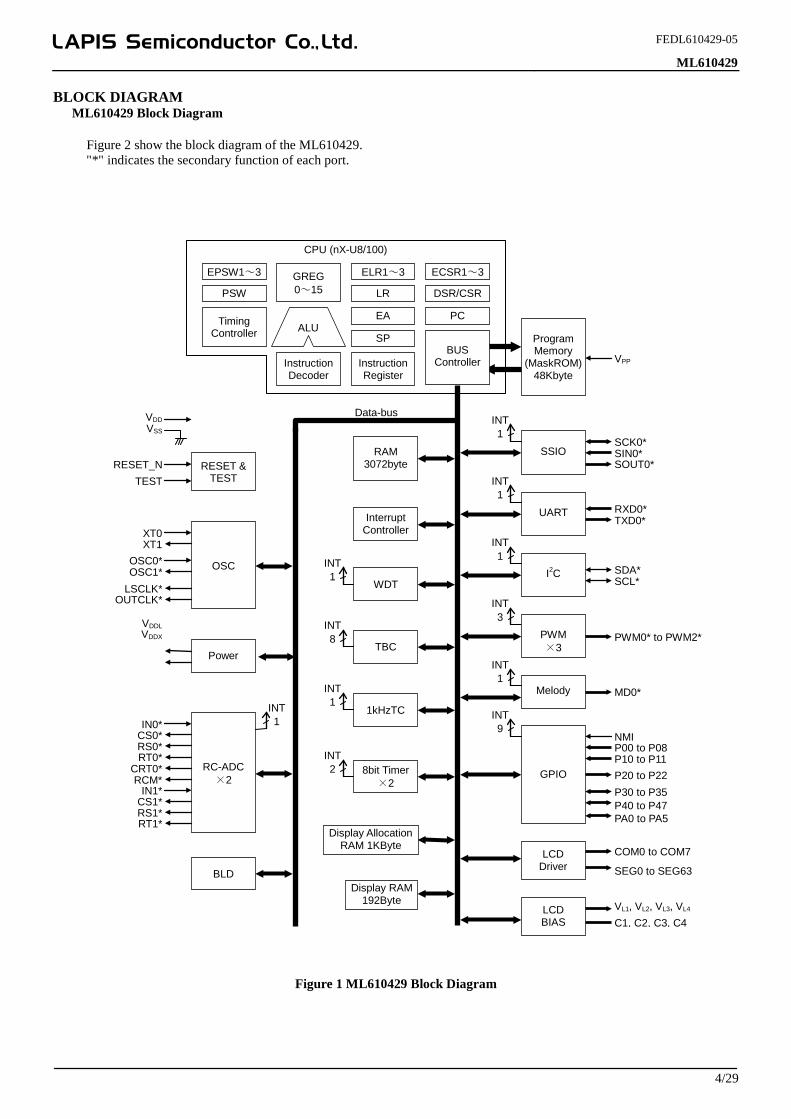
BLOCK DIAGRAM ML610429 Block Diagram
Figure 2 show the block diagram of the ML610429. "*" indicates the secondary function of each port.
Figure 1 ML610429 Block Diagram
Program Memory
(MaskROM) 48Kbyte
SSIO SCK0* SIN0* SOUT0*
UART RXD0* TXD0*
I2C SDA* SCL*
INT 1
RAM 3072byte
Interrupt Controller
CPU (nX-U8/100)
Timing Controller
EA
SP
Instruction Decoder
BUS Controller Instruction
Register
TBC
INT 8
INT 1
INT 1 INT
1 WDT
INT 2 8bit Timer
×2
INT 3
PWM ×3
GPIO
P00 to P08 P10 to P11 P20 to P22
INT 9
NMI
P30 to P35 P40 to P47
Data-bus
PWM0* to PWM2*
Melody
INT 1
MD0*
TEST RESET_N
OSC
XT0 XT1
OSC0* OSC1*
LSCLK* OUTCLK*
BLD
Power
VDDL
LCD Driver
COM0 to COM7
SEG0 to SEG63
LCD BIAS
VL1, VL2, VL3, VL4 C1, C2, C3, C4
RC-ADC ×2
CS0* IN0*
RS0* RT0*
CRT0* RCM*
CS1* IN1*
RS1* RT1*
RESET & TEST
ALU
EPSW1~3 PSW
ELR1~3 LR
ECSR1~3 DSR/CSR PC
GREG 0~15
VPP
VDD VSS
VDDX
1kHzTC
INT 1 INT
1
Display RAM 192Byte
Display Allocation RAM 1KByte
PA0 to PA5
FEDL610429-05
ML610429
5/29
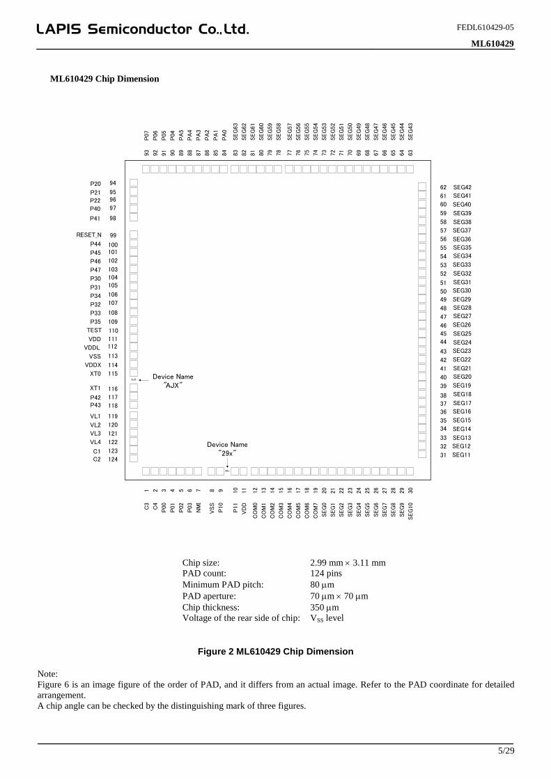
ML610429 Chip Dimension
Chip size: 2.99 mm × 3.11 mm PAD count: 124 pins Minimum PAD pitch: 80 µm PAD aperture: 70 µm × 70 µm Chip thickness: 350 µm Voltage of the rear side of chip: VSS level
Figure 2 ML610429 Chip Dimension Note: Figure 6 is an image figure of the order of PAD, and it differs from an actual image. Refer to the PAD coordinate for detailed arrangement. A chip angle can be checked by the distinguishing mark of three figures.
29x
AJX
Device Name " 29x "
Device Name " AJX "
31 32 33 34 35 36 37 38 39 40 41 42 43 44 45 46 47 48 49 50 51 52 53 54 55 56 57 58 59 60 61 62 SEG42
SEG41 SEG40 SEG39 SEG38 SEG37 SEG36 SEG35 SEG34 SEG33 SEG32 SEG31 SEG30 SEG29 SEG28 SEG27 SEG26 SEG25 SEG24 SEG23 SEG22 SEG21 SEG20 SEG19 SEG18 SEG17 SEG16 SEG15 SEG14 SEG13 SEG12 SEG11
94 P20 95 96 97 98
99 RESET_N 100 P44 101 P45 102 P46 103 P47 104 P30 105 P31 106 P34 107 P32 108 P33 109 P35 110 TEST 111 VDD 112 VDDL 113 VSS 114 VDDX 115 XT0 116 XT1 117 P42 118 P43 119 VL1 120 VL2 121 VL3 122 VL4 123 C1 124 C2
P21 P22 P40 P41
61 SEG41
62 SEG42
SEG
43
63
SEG
44
64
SEG
45
65
SEG
46
66
SEG
47
67
SEG
48
68
SEG
49
69
SEG
50
70
SEG
51
71
SEG
52
72
SEG
53
73
SEG
54
74
SEG
55
75
SEG
56
76
SEG
57
77
78
SEG
58
79
SEG
59
80
SEG
60
81
SEG
61
82
SEG
62
83
SEG
63
84
PA
0
85
PA
1
86
PA
2
87
PA
3
88
PA
4
89
PA
5
90
P04
91
P05
92
93
P06
P07
94P20
95P21
C3
1
C4
2
P00
3
P01
4
P02
5
P03
6
NM
I7
VSS
8
P10
9
P11
10
VD
D11
CO
M0
12
CO
M1
13
CO
M2
14
CO
M3
15
CO
M4
16
CO
M5
17
CO
M6
18
CO
M7
19
SEG
020
SEG
121
SEG
222
SEG
323
SEG
424
SEG
525
SEG
626
SEG
727
SEG
828
SEG
929
SEG
1030
FEDL610429-05
ML610429
6/29
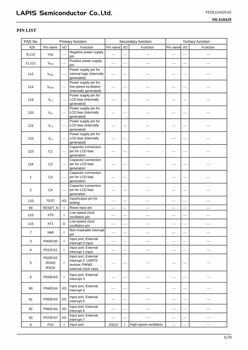
PIN LIST
PAD No. Primary function Secondary function Tertiary function 429 Pin name I/O Function Pin name I/O Function Pin name I/O Function
8,113 Vss Negative power supply pin
11,111 VDD Positive power supply pin
112 VDDL Power supply pin for internal logic (internally generated)
114 VDDX Power supply pin for low-speed oscillation (internally generated)
119 VL1 Power supply pin for LCD bias (internally generated)
120 VL2 Power supply pin for LCD bias (internally generated)
121 VL3 Power supply pin for LCD bias (internally generated)
122 VL4 Power supply pin for LCD bias (internally generated)
123 C1 Capacitor connection pin for LCD bias generation
124 C2 Capacitor connection pin for LCD bias generation
1 C3 Capacitor connection pin for LCD bias generation
2 C4 Capacitor connection pin for LCD bias generation
110 TEST I/O Input/output pin for testing
99 RESET_N I Reset input pin
115 XT0 I Low-speed clock oscillation pin
116 XT1 O Low-speed clock oscillation pin
7 NMI I Non-maskable interrupt pin
3 P00/EXI0 I Input port, External interrupt 0 input
4 P01/EXI1 I Input port, External interrupt 1 input
5 P02/EXI2
/RXD0 /P2CK
I
Input port, External interrupt 2, UART0 receive, PWM2 external clock input
6 P03/EXI3 I Input port, External interrupt 3
90 P04/EXI4 I/O Input port, External interrupt 4
91 P05/EXI5 I/O Input port, External interrupt 5
92 P06/EXI6 I/O Input port, External interrupt 6
93 P07/EXI7 I/O Input port, External interrupt 7
9 P10 I Input port OSC0 I High-speed oscillation
FEDL610429-05
ML610429
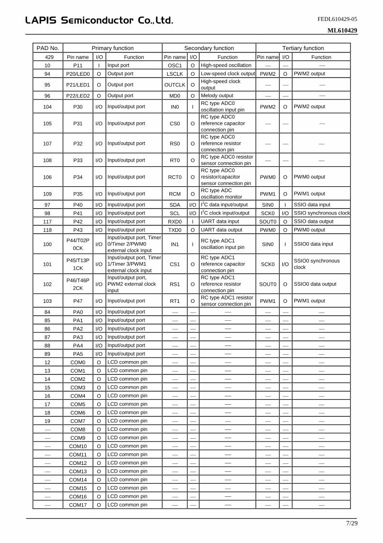
7/29
PAD No. Primary function Secondary function Tertiary function 429 Pin name I/O Function Pin name I/O Function Pin name I/O Function 10 P11 I Input port OSC1 O High-speed oscillation
94 P20/LED0 O Output port LSCLK O Low-speed clock output PWM2 O PWM2 output
95 P21/LED1 O Output port OUTCLK O High-speed clock output
96 P22/LED2 O Output port MD0 O Melody output
104 P30 I/O Input/output port IN0 I RC type ADC0 oscillation input pin PWM2 O PWM2 output
105 P31 I/O Input/output port CS0 O RC type ADC0 reference capacitor connection pin
107 P32 I/O Input/output port RS0 O RC type ADC0 reference resistor connection pin
108 P33 I/O Input/output port RT0 O RC type ADC0 resistor sensor connection pin
106 P34 I/O Input/output port RCT0 O RC type ADC0 resistor/capacitor sensor connection pin
PWM0 O PWM0 output
109 P35 I/O Input/output port RCM O RC type ADC oscillation monitor PWM1 O PWM1 output
97 P40 I/O Input/output port SDA I/O I2C data input/output SIN0 I SSIO data input
98 P41 I/O Input/output port SCL I/O I2C clock input/output SCK0 I/O SSIO synchronous clock
117 P42 I/O Input/output port RXD0 I UART data input SOUT0 O SSIO data output
118 P43 I/O Input/output port TXD0 O UART data output PWM0 O PWM0 output
100 P44/T02P
0CK I/O
Input/output port, Timer 0/Timer 2/PWM0 external clock input
IN1 I RC type ADC1 oscillation input pin SIN0 I SSIO0 data input
101 P45/T13P
1CK I/O
Input/output port, Timer 1/Timer 3/PWM1 external clock input
CS1 O RC type ADC1 reference capacitor connection pin
SCK0 I/O SSIO0 synchronous clock
102 P46/T46P
2CK I/O
Input/output port, PWM2 external clock input
RS1 O RC type ADC1 reference resistor connection pin
SOUT0 O SSIO0 data output
103 P47 I/O Input/output port RT1 O RC type ADC1 resistor sensor connection pin PWM1 O PWM1 output
84 PA0 I/O Input/output port 85 PA1 I/O Input/output port 86 PA2 I/O Input/output port 87 PA3 I/O Input/output port 88 PA4 I/O Input/output port 89 PA5 I/O Input/output port 12 COM0 O LCD common pin 13 COM1 O LCD common pin 14 COM2 O LCD common pin 15 COM3 O LCD common pin 16 COM4 O LCD common pin 17 COM5 O LCD common pin 18 COM6 O LCD common pin 19 COM7 O LCD common pin COM8 O LCD common pin COM9 O LCD common pin COM10 O LCD common pin COM11 O LCD common pin COM12 O LCD common pin COM13 O LCD common pin COM14 O LCD common pin COM15 O LCD common pin COM16 O LCD common pin COM17 O LCD common pin
FEDL610429-05
ML610429
8/29
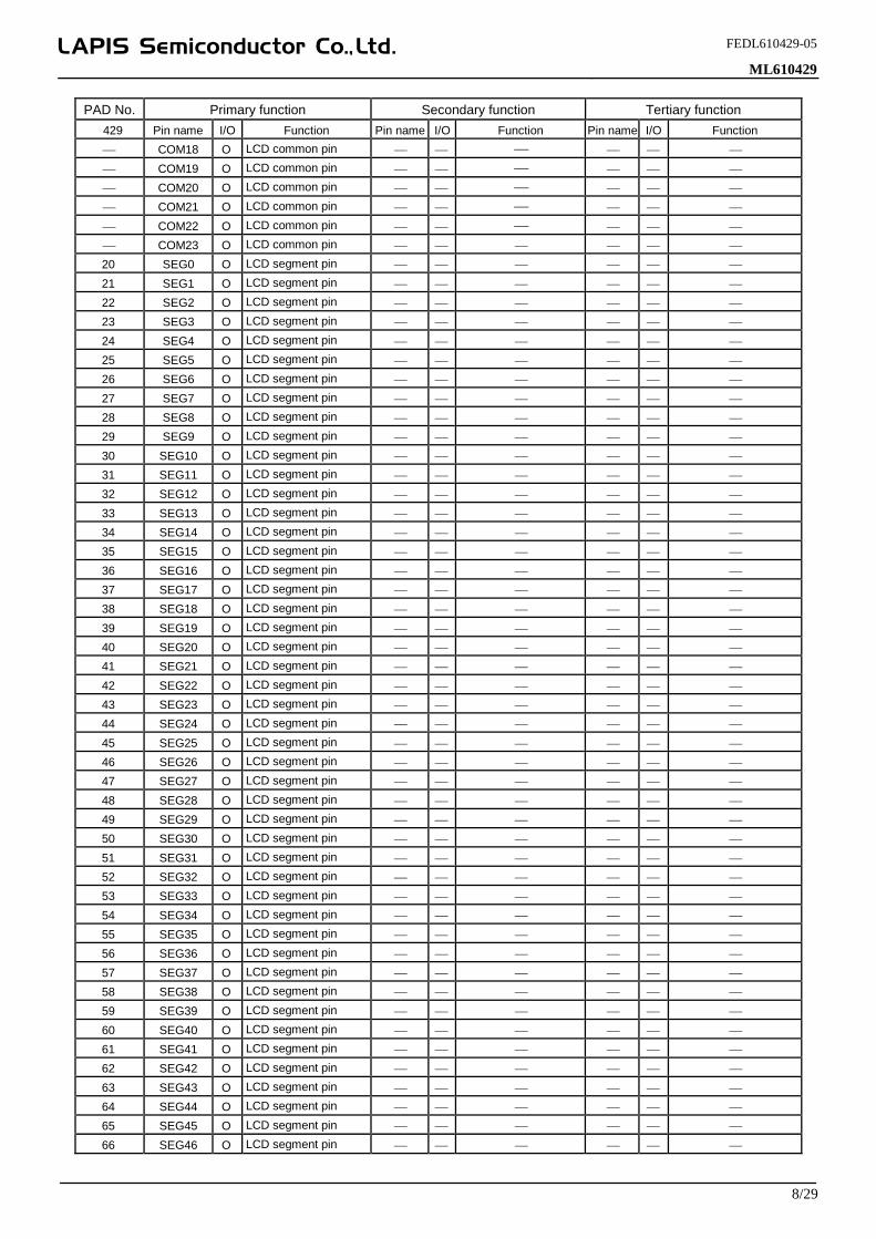
PAD No. Primary function Secondary function Tertiary function 429 Pin name I/O Function Pin name I/O Function Pin name I/O Function COM18 O LCD common pin COM19 O LCD common pin COM20 O LCD common pin COM21 O LCD common pin COM22 O LCD common pin COM23 O LCD common pin 20 SEG0 O LCD segment pin 21 SEG1 O LCD segment pin 22 SEG2 O LCD segment pin 23 SEG3 O LCD segment pin 24 SEG4 O LCD segment pin 25 SEG5 O LCD segment pin 26 SEG6 O LCD segment pin 27 SEG7 O LCD segment pin 28 SEG8 O LCD segment pin 29 SEG9 O LCD segment pin 30 SEG10 O LCD segment pin 31 SEG11 O LCD segment pin 32 SEG12 O LCD segment pin 33 SEG13 O LCD segment pin 34 SEG14 O LCD segment pin 35 SEG15 O LCD segment pin 36 SEG16 O LCD segment pin 37 SEG17 O LCD segment pin 38 SEG18 O LCD segment pin 39 SEG19 O LCD segment pin 40 SEG20 O LCD segment pin 41 SEG21 O LCD segment pin 42 SEG22 O LCD segment pin 43 SEG23 O LCD segment pin 44 SEG24 O LCD segment pin 45 SEG25 O LCD segment pin 46 SEG26 O LCD segment pin 47 SEG27 O LCD segment pin 48 SEG28 O LCD segment pin 49 SEG29 O LCD segment pin 50 SEG30 O LCD segment pin 51 SEG31 O LCD segment pin 52 SEG32 O LCD segment pin 53 SEG33 O LCD segment pin 54 SEG34 O LCD segment pin 55 SEG35 O LCD segment pin 56 SEG36 O LCD segment pin 57 SEG37 O LCD segment pin 58 SEG38 O LCD segment pin 59 SEG39 O LCD segment pin 60 SEG40 O LCD segment pin 61 SEG41 O LCD segment pin 62 SEG42 O LCD segment pin 63 SEG43 O LCD segment pin 64 SEG44 O LCD segment pin 65 SEG45 O LCD segment pin 66 SEG46 O LCD segment pin
FEDL610429-05
ML610429
9/29
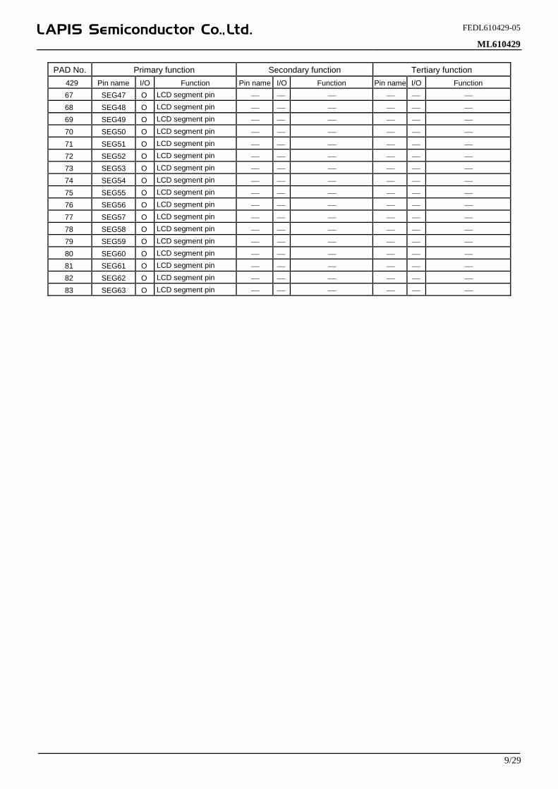
PAD No. Primary function Secondary function Tertiary function 429 Pin name I/O Function Pin name I/O Function Pin name I/O Function 67 SEG47 O LCD segment pin 68 SEG48 O LCD segment pin 69 SEG49 O LCD segment pin 70 SEG50 O LCD segment pin 71 SEG51 O LCD segment pin 72 SEG52 O LCD segment pin 73 SEG53 O LCD segment pin 74 SEG54 O LCD segment pin 75 SEG55 O LCD segment pin 76 SEG56 O LCD segment pin 77 SEG57 O LCD segment pin 78 SEG58 O LCD segment pin 79 SEG59 O LCD segment pin 80 SEG60 O LCD segment pin 81 SEG61 O LCD segment pin 82 SEG62 O LCD segment pin 83 SEG63 O LCD segment pin
FEDL610429-05
ML610429
10/29
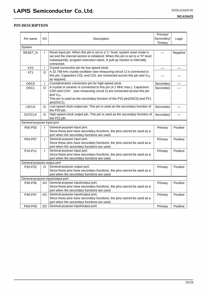
PIN DESCRIPTION
Pin name I/O Description Primary/
Secondary/ Tertiary
Logic
System
RESET_N I Reset input pin. When this pin is set to a “L” level, system reset mode is set and the internal section is initialized. When this pin is set to a “H” level subsequently, program execution starts. A pull-up resistor is internally connected.
— Negative
XT0 I Crystal connection pin for low-speed clock. A 32.768 kHz crystal oscillator (see measuring circuit 1) is connected to this pin. Capacitors CDL and CGL are connected across this pin and VSS as required.
— — XT1 O
— —
OSC0 I Crystal/ceramic connection pin for high-speed clock. A crystal or ceramic is connected to this pin (4.1 MHz max.). Capacitors CDH and CGH (see measuring circuit 1) are connected across this pin and VSS. This pin is used as the secondary function of the P10 pin(OSC0) and P11 pin(OSC1).
Secondary — OSC1 O Secondary —
LSCLK O Low-speed clock output pin. This pin is used as the secondary function of the P20 pin.
Secondary —
OUTCLK O High-speed clock output pin. This pin is used as the secondary function of the P21 pin.
Secondary —
General-purpose input port P00-P03
I General-purpose input port.
Since these pins have secondary functions, the pins cannot be used as a port when the secondary functions are used.
Primary Positive
P04-P07
I General-purpose input port. Since these pins have secondary functions, the pins cannot be used as a port when the secondary functions are used.
Primary Positive
P10-P11 I General-purpose input port. Since these pins have secondary functions, the pins cannot be used as a port when the secondary functions are used.
Primary Positive
General-purpose output port P20-P22 O General-purpose output port.
Since these pins have secondary functions, the pins cannot be used as a port when the secondary functions are used.
Primary Positive
General-purpose input/output port P30-P35 I/O General-purpose input/output port.
Since these pins have secondary functions, the pins cannot be used as a port when the secondary functions are used.
Primary Positive
P40-P47 I/O General-purpose input/output port. Since these pins have secondary functions, the pins cannot be used as a port when the secondary functions are used.
Primary Positive
PA0-PA5 I/O General-purpose input/output port. Primary Positive
FEDL610429-05
ML610429
11/29
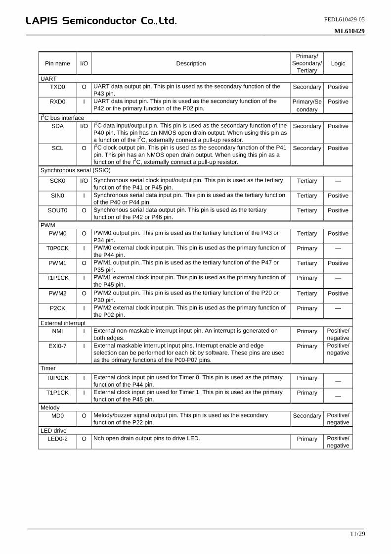
Pin name I/O Description Primary/
Secondary/ Tertiary
Logic
UART TXD0 O UART data output pin. This pin is used as the secondary function of the
P43 pin. Secondary Positive
RXD0 I UART data input pin. This pin is used as the secondary function of the P42 or the primary function of the P02 pin.
Primary/Secondary
Positive
I2C bus interface SDA I/O I2C data input/output pin. This pin is used as the secondary function of the
P40 pin. This pin has an NMOS open drain output. When using this pin as a function of the I2C, externally connect a pull-up resistor.
Secondary Positive
SCL O I2C clock output pin. This pin is used as the secondary function of the P41 pin. This pin has an NMOS open drain output. When using this pin as a function of the I2C, externally connect a pull-up resistor.
Secondary Positive
Synchronous serial (SSIO)
SCK0 I/O Synchronous serial clock input/output pin. This pin is used as the tertiary function of the P41 or P45 pin.
Tertiary —
SIN0 I Synchronous serial data input pin. This pin is used as the tertiary function of the P40 or P44 pin.
Tertiary Positive
SOUT0 O Synchronous serial data output pin. This pin is used as the tertiary function of the P42 or P46 pin.
Tertiary Positive
PWM PWM0 O PWM0 output pin. This pin is used as the tertiary function of the P43 or
P34 pin. Tertiary Positive
T0P0CK I PWM0 external clock input pin. This pin is used as the primary function of the P44 pin.
Primary —
PWM1 O PWM1 output pin. This pin is used as the tertiary function of the P47 or P35 pin.
Tertiary Positive
T1P1CK I PWM1 external clock input pin. This pin is used as the primary function of the P45 pin.
Primary —
PWM2 O PWM2 output pin. This pin is used as the tertiary function of the P20 or P30 pin.
Tertiary Positive
P2CK I PWM2 external clock input pin. This pin is used as the primary function of the P02 pin.
Primary —
External interrupt NMI I External non-maskable interrupt input pin. An interrupt is generated on
both edges. Primary Positive/
negative EXI0-7 I External maskable interrupt input pins. Interrupt enable and edge
selection can be performed for each bit by software. These pins are used as the primary functions of the P00-P07 pins.
Primary Positive/ negative
Timer T0P0CK I External clock input pin used for Timer 0. This pin is used as the primary
function of the P44 pin. Primary —
T1P1CK I External clock input pin used for Timer 1. This pin is used as the primary function of the P45 pin.
Primary —
Melody MD0 O Melody/buzzer signal output pin. This pin is used as the secondary
function of the P22 pin. Secondary Positive/
negative LED drive
LED0-2 O Nch open drain output pins to drive LED. Primary Positive/ negative
FEDL610429-05
ML610429
12/29
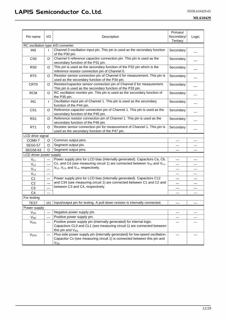
Pin name I/O Description Primary/
Secondary/ Tertiary
Logic
RC oscillation type A/D converter IN0 I Channel 0 oscillation input pin. This pin is used as the secondary function
of the P30 pin. Secondary —
CS0 O Channel 0 reference capacitor connection pin. This pin is used as the secondary function of the P31 pin.
Secondary —
RS0 O This pin is used as the secondary function of the P32 pin which is the reference resistor connection pin of Channel 0.
Secondary —
RT0 O Resistor sensor connection pin of Channel 0 for measurement. This pin is used as the secondary function of the P34 pin.
Secondary —
CRT0 O Resistor/capacitor sensor connection pin of Channel 0 for measurement. This pin is used as the secondary function of the P33 pin.
Secondary —
RCM O RC oscillation monitor pin. This pin is used as the secondary function of the P35 pin.
Secondary —
IN1 I Oscillation input pin of Channel 1. This pin is used as the secondary function of the P44 pin.
Secondary —
CS1 O Reference capacitor connection pin of Channel 1. This pin is used as the secondary function of the P45 pin.
Secondary —
RS1 O Reference resistor connection pin of Channel 1. This pin is used as the secondary function of the P46 pin.
Secondary —
RT1 O Resistor sensor connection pin for measurement of Channel 1. This pin is used as the secondary function of the P47 pin.
Secondary —
LCD drive signal COM0-7 O Common output pins. — — SEG0-57 O Segment output pin. — —
SEG58-63 O Segment output pins. — — LCD driver power supply
VL1 — Power supply pins for LCD bias (internally generated). Capacitors Ca, Cb, Cc, and Cd (see measuring circuit 1) are connected between VSS and VL1, VL2, VL3, and VL4, respectively.
— — VL2 — — — VL3 — — — VL4 — — — C1 — Power supply pins for LCD bias (internally generated). Capacitors C12
and C34 (see measuring circuit 1) are connected between C1 and C2 and between C3 and C4, respectively.
— — C2 — — — C3 — — — C4 — — —
For testing TEST I/O Input/output pin for testing. A pull-down resistor is internally connected. — —
Power supply VSS — Negative power supply pin. — — VDD — Positive power supply pin. — — VDDL — Positive power supply pin (internally generated) for internal logic.
Capacitors CL0 and CL1 (see measuring circuit 1) are connected between this pin and VSS.
— —
VDDX — Plus-side power supply pin (internally generated) for low-speed oscillation. Capacitor Cx (see measuring circuit 1) is connected between this pin and VSS.
— —

FEDL610429-05
ML610429
13/29
TERMINATION OF UNUSED PINS Table 3 shows methods of terminating the unused pins.
Table 3 Termination of Unused Pins
Pin Recommended pin termination VPP Open VL1, VL2, VL3, VL4 Open C1, C2, C3, C4 Open RESET_N Open TEST Open NMI Open P00 to P07 VDD or VSS P10 to P11 VDD P20 to P22 Open P30 to P35 Open P40 to P47 Open PA0 to PA5 Open COM0 to 23 Open SEG0 to 63 Open
Note: It is recommended to set the unused input ports and input/output ports to the inputs with pull-down resistors/pull-up resistors or the output mode since the supply current may become excessively large if the pins are left open in the high impedance input setting.

FEDL610429-05
ML610429
14/29
DIFFERENCES BETWEEN MASKROM VERSION and FLASHROM VERSION This section describes differences between ML610429 (MaskROM version) and ML610Q429 (FlashROM version). PAD Number
The PAD number is changed. In MaskROM version, VPP pin which is power supply pin for Flash ROM was deleted.
On-Chip debug function
There is not On-Chip debug dunction in MaskROM version. Chip behavior by RESET_N pin
The following table describes the difference of ML610429 and ML610Q428/ML610Q429 about RESET_N.
Table 5 Differences of ML610429 and ML610Q428/ML610Q429 about RESET_N
ML610429 (MaskROM version)
ML610Q428/ML610Q429 (FlashROM version)
Internal power supply (vddl, vddx)
is shutdown by RESET_N. is not shutdown by RESET_N. vddl and vddx keep power on.
POR bit of RSTAT is set to “1” after negating RESET_N, if activating period is long.
is set nothing. There is no register flag by RESET_N.
ALL LSI pin directions are not fixed during RESET_N is activated. After negating, those pin are fixed to “Z” normally.
are fixed to “Z” by RESET_N.
Figure 7 show Chip behavior by RESET_N pin.
VDD
RESET_N
MASKROM version
FlashROM version
VDDL,VDDX
VDDL,VDDX
RSTAT
PIN Direction
RSTAT
PIN Direction
RESET_N activates during power up RESET_N activates for long time
Hi-Z Hi-Z
000b
001b
Hi-Z Unknown
not power off
Hi-Z Unknown
possibility power off
Figure 7 Chip behavior by RESET_N pin
FEDL610429-05
ML610429
15/29
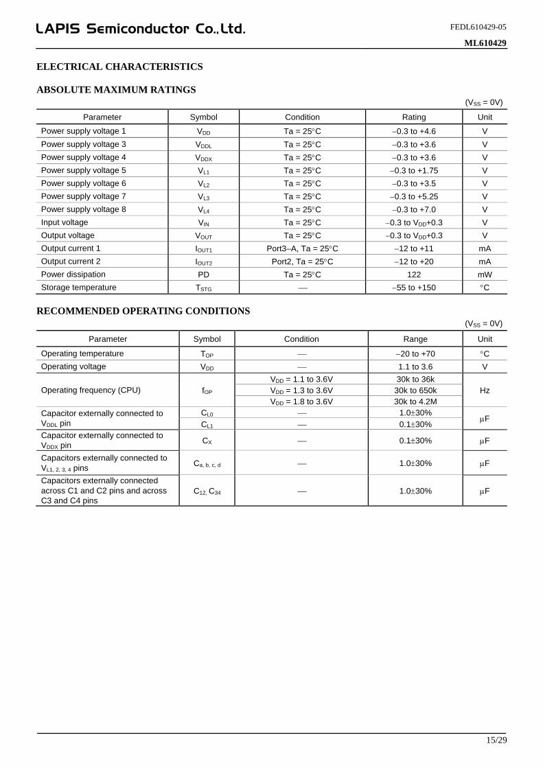
ELECTRICAL CHARACTERISTICS ABSOLUTE MAXIMUM RATINGS
(VSS = 0V)
Parameter Symbol Condition Rating Unit
Power supply voltage 1 VDD Ta = 25°C −0.3 to +4.6 V Power supply voltage 3 VDDL Ta = 25°C −0.3 to +3.6 V Power supply voltage 4 VDDX Ta = 25°C −0.3 to +3.6 V Power supply voltage 5 VL1 Ta = 25°C −0.3 to +1.75 V Power supply voltage 6 VL2 Ta = 25°C −0.3 to +3.5 V Power supply voltage 7 VL3 Ta = 25°C −0.3 to +5.25 V Power supply voltage 8 VL4 Ta = 25°C −0.3 to +7.0 V Input voltage VIN Ta = 25°C −0.3 to VDD+0.3 V Output voltage VOUT Ta = 25°C −0.3 to VDD+0.3 V Output current 1 IOUT1 Port3–A, Ta = 25°C −12 to +11 mA Output current 2 IOUT2 Port2, Ta = 25°C −12 to +20 mA Power dissipation PD Ta = 25°C 122 mW Storage temperature TSTG −55 to +150 °C
RECOMMENDED OPERATING CONDITIONS
(VSS = 0V)
Parameter Symbol Condition Range Unit
Operating temperature TOP −20 to +70 °C Operating voltage VDD 1.1 to 3.6 V
Operating frequency (CPU) fOP VDD = 1.1 to 3.6V 30k to 36k
Hz VDD = 1.3 to 3.6V 30k to 650k VDD = 1.8 to 3.6V 30k to 4.2M
Capacitor externally connected to VDDL pin
CL0 1.0±30% µF
CL1 0.1±30% Capacitor externally connected to VDDX pin CX 0.1±30% µF
Capacitors externally connected to VL1, 2, 3, 4 pins Ca, b, c, d 1.0±30% µF
Capacitors externally connected across C1 and C2 pins and across C3 and C4 pins
C12, C34 1.0±30% µF
FEDL610429-05
ML610429
16/29
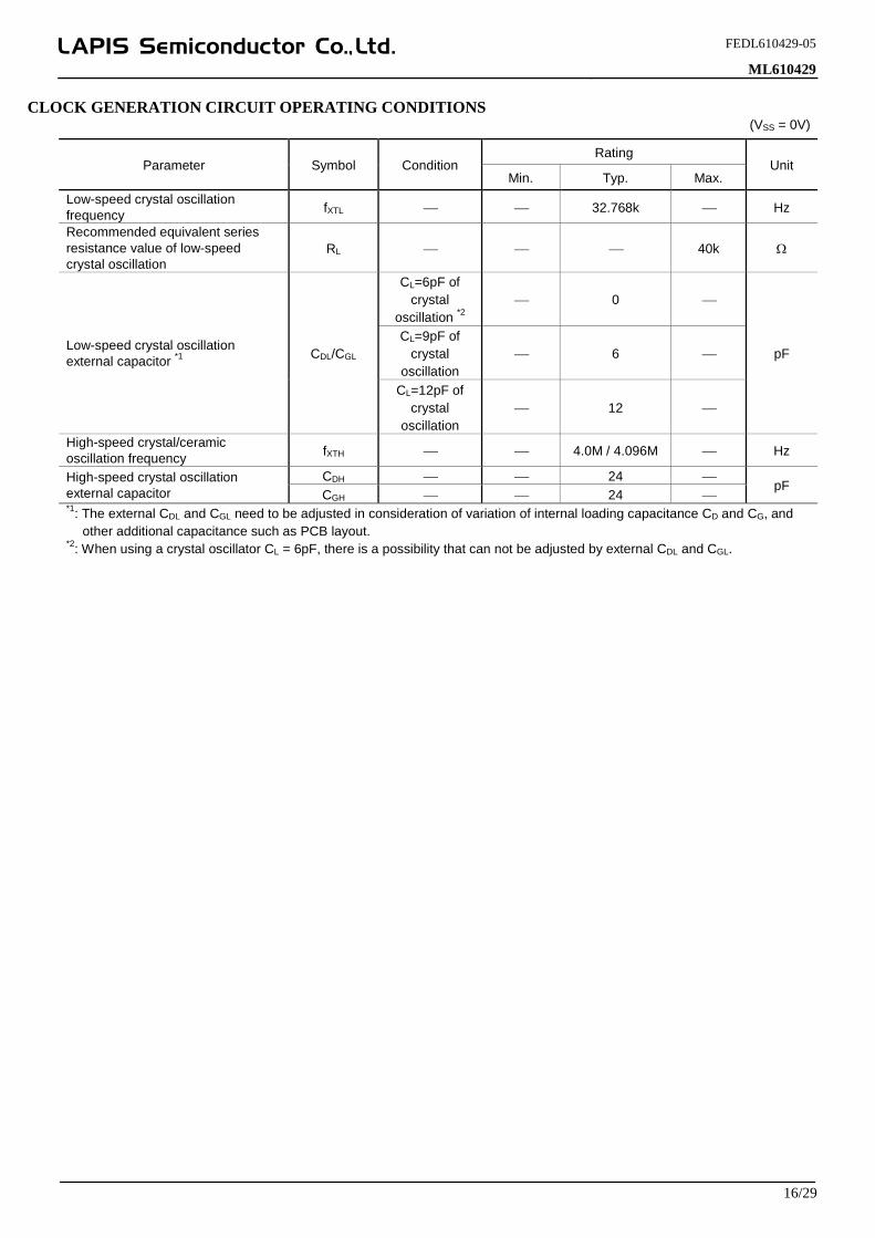
CLOCK GENERATION CIRCUIT OPERATING CONDITIONS (VSS = 0V)
Parameter Symbol Condition Rating
Unit Min. Typ. Max.
Low-speed crystal oscillation frequency fXTL 32.768k Hz
Recommended equivalent series resistance value of low-speed crystal oscillation
RL 40k Ω
Low-speed crystal oscillation external capacitor *1 CDL/CGL
CL=6pF of crystal
oscillation *2 0
pF CL=9pF of
crystal oscillation
6
CL=12pF of crystal
oscillation 12
High-speed crystal/ceramic oscillation frequency fXTH 4.0M / 4.096M Hz
High-speed crystal oscillation external capacitor
CDH 24 pF
CGH 24 *1: The external CDL and CGL need to be adjusted in consideration of variation of internal loading capacitance CD and CG, and
other additional capacitance such as PCB layout. *2: When using a crystal oscillator CL = 6pF, there is a possibility that can not be adjusted by external CDL and CGL.
FEDL610429-05
ML610429
17/29
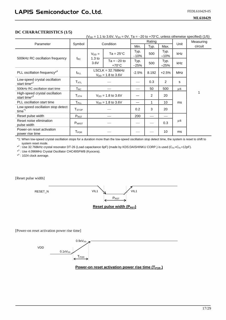
DC CHARACTERISTICS (1/5)
(VDD = 1.1 to 3.6V, VSS = 0V, Ta = −20 to +70°C, unless otherwise specified) (1/5)
Parameter Symbol Condition Rating
Unit Measuring
circuit Min. Typ. Max.
500kHz RC oscillation frequency fRC VDD = 1.3 to 3.6V
Ta = 25°C Typ.
−10% 500
Typ. +10%
kHz
1
Ta = −20 to +70°C
Typ. −25%
500 Typ.
+25% kHz
PLL oscillation frequency*4 fPLL LSCLK = 32.768kHz
VDD = 1.8 to 3.6V -2.5% 8.192 +2.5% MHz
Low-speed crystal oscillation start time*2 TXTL 0.3 2 s
500kHz RC oscillation start time TRC 50 500 µs High-speed crystal oscillation start time*3 TXTH VDD = 1.8 to 3.6V ― 2 20
ms PLL oscillation start time TPLL VDD = 1.8 to 3.6V ― 1 10 Low-speed oscillation stop detect time*1 TSTOP 0.2 3 20
Reset pulse width PRST 200 µs Reset noise elimination
pulse width PNRST 0.3
Power-on reset activation power rise time TPOR 10 ms
*1: When low-speed crystal oscillation stops for a duration more than the low-speed oscillation stop detect time, the system is reset to shift to system reset mode.
*2 : Use 32.768kHz crystal resonator DT-26 (Load capacitance 6pF) (made by KDS:DAISHINKU CORP.) is used (CGL=CDL=12pF). *3 : Use 4.096MHz Crystal Oscillator CHC49SFWB (Kyocera). *4 : 1024 clock average.
[Reset pulse width] [Power-on reset activation power rise time]
RESET_N
Reset pulse width (PRST)
PRST
VIL1 VIL1
VDD
0.9xVDD
0.1xVDD TPOR
Power-on reset activation power rise time (TPOR )
FEDL610429-05
ML610429
18/29
DC CHARACTERISTICS (2/5)
(VDD = 1.1 to 3.6V, VSS = 0V, Ta = −20 to +70°C, unless otherwise specified) (2/5)
Parameter Symbol Condition Rating
Unit Measuring
circuit Min. Typ. Max.
VL1 voltage VL1 VDD = 3.0V, Tj = 25°C
CN4–0 = 00H 0.89 0.94 0.99
V
1
CN4–0 = 01H 0.91 0.96 1.01 CN4–0 = 02H 0.93 0.98 1.03 CN4–0 = 03H 0.95 1.00 1.05 CN4–0 = 04H 0.97 1.02 1.07 CN4–0 = 05H 0.99 1.04 1.09 CN4–0 = 06H 1.01 1.06 1.11 CN4–0 = 07H 1.03 1.08 1.13 CN4–0 = 08H 1.05 1.10 1.15 CN4–0 = 09H 1.07 1.12 1.17 CN4–0 = 0AH 1.09 1.14 1.19 CN4–0 = 0BH 1.11 1.16 1.21 CN4–0 = 0CH 1.13 1.18 1.23 CN4–0 = 0DH 1.15 1.20 1.25 CN4–0 = 0EH 1.17 1.22 1.27 CN4–0 = 0FH 1.19 1.24 1.29 CN4–0 = 10H 1.21 1.26 1.31 CN4–0 = 11H 1.23 1.28 1.33 CN4–0 = 12H 1.25 1.30 1.35 CN4–0 = 13H 1.27 1.32 1.37
CN4–0 = 14H *1 1.29 1.34 1.39 CN4–0 = 15H *1 1.31 1.36 1.41 CN4–0 = 16H *1 1.33 1.38 1.43 CN4–0 = 17H *1 1.35 1.40 1.45 CN4–0 = 18H *1 1.37 1.42 1.47 CN4–0 = 19H *1 1.39 1.44 1.49 CN4–0 = 1AH *1 1.41 1.46 1.51 CN4–0 = 1BH *1 1.43 1.48 1.53 CN4–0 = 1CH *1 1.45 1.50 1.55 CN4–0 = 1DH *1 1.47 1.52 1.57 CN4–0 = 1EH *1 1.49 1.54 1.59 CN4–0 = 1FH *1 1.51 1.56 1.61
VL1 temperature deviation ∆VL1 VDD = 3.0V −1.5 mV/°C
VL1 voltage dependency ∆VL1 VDD = 1.3 to 3.6V 5 20 mV/V
VL2 voltage VL2 VDD = 3.0V, Tj = 25°C 300kΩ load (VL4−VSS)
Typ. −10%
VL1×2 Typ. +4%
V VL3 voltage VL3 VDD = 3.0V, Tj = 25°C
300kΩ load (VL4−VSS)
1/3 bias Typ. −10%
VL1×2 Typ. +4% 1/4 bias VL1×3
VL4 voltage VL4 1/3 bias Typ.
−10% VL1×3 Typ.
+5% 1/4 bias VL1×4 LCD bias voltage generation time TBIAS 600 ms
*1: When using 1/4 bias, the VL1 voltage is set to typ. 1.32 V (same voltage as in CN4–0 = 13H).
FEDL610429-05
ML610429
19/29
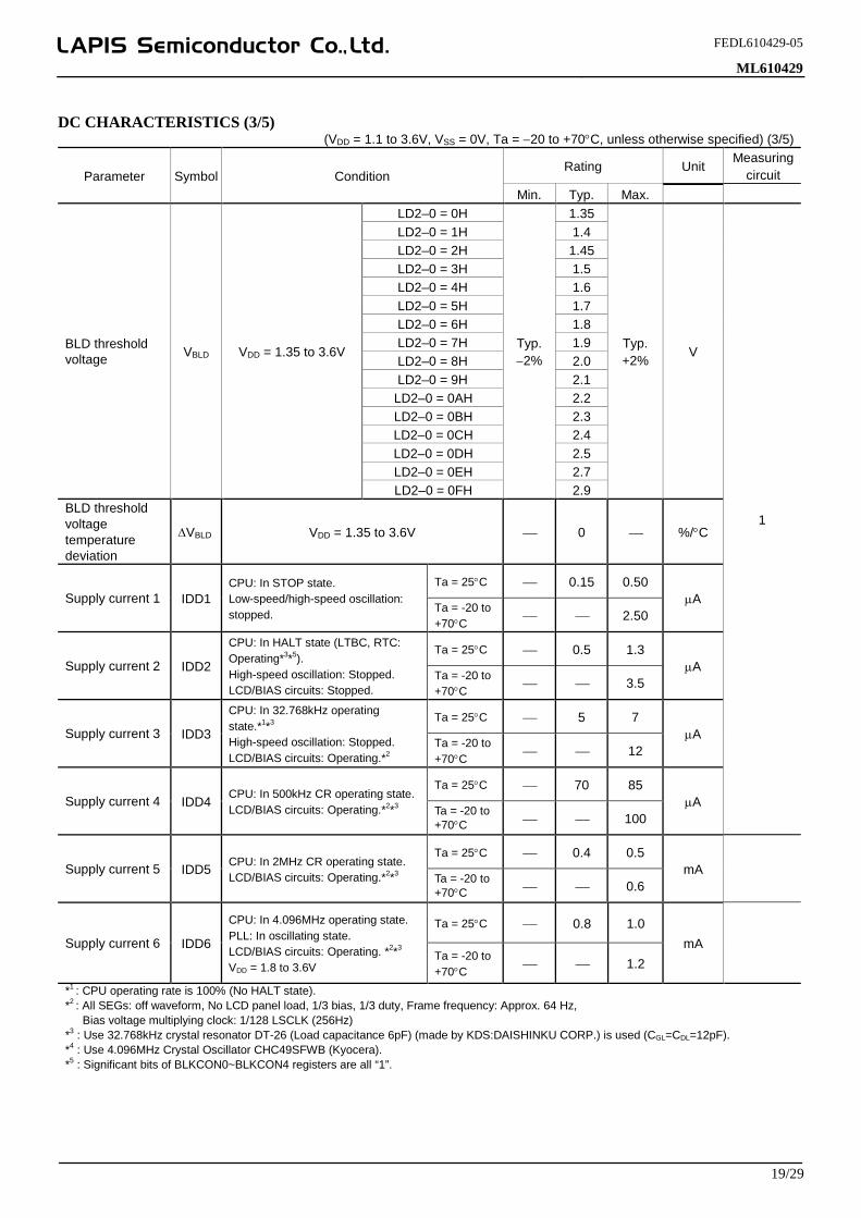
DC CHARACTERISTICS (3/5)
(VDD = 1.1 to 3.6V, VSS = 0V, Ta = −20 to +70°C, unless otherwise specified) (3/5)
Parameter Symbol Condition Rating Unit
Measuring circuit
Min. Typ. Max.
BLD threshold voltage VBLD VDD = 1.35 to 3.6V
LD2–0 = 0H
Typ. −2%
1.35
Typ. +2%
V
1
LD2–0 = 1H 1.4 LD2–0 = 2H 1.45 LD2–0 = 3H 1.5 LD2–0 = 4H 1.6 LD2–0 = 5H 1.7 LD2–0 = 6H 1.8 LD2–0 = 7H 1.9 LD2–0 = 8H 2.0 LD2–0 = 9H 2.1
LD2–0 = 0AH 2.2 LD2–0 = 0BH 2.3 LD2–0 = 0CH 2.4 LD2–0 = 0DH 2.5 LD2–0 = 0EH 2.7 LD2–0 = 0FH 2.9
BLD threshold voltage temperature deviation
∆VBLD VDD = 1.35 to 3.6V 0 %/°C
Supply current 1 IDD1 CPU: In STOP state. Low-speed/high-speed oscillation: stopped.
Ta = 25°C 0.15 0.50 µA
Ta = -20 to +70°C 2.50
Supply current 2 IDD2
CPU: In HALT state (LTBC, RTC: Operating*3*5). High-speed oscillation: Stopped. LCD/BIAS circuits: Stopped.
Ta = 25°C 0.5 1.3 µA
Ta = -20 to +70°C 3.5
Supply current 3 IDD3
CPU: In 32.768kHz operating state.*1*3
High-speed oscillation: Stopped. LCD/BIAS circuits: Operating.*2
Ta = 25°C 5 7 µA
Ta = -20 to +70°C 12
Supply current 4 IDD4 CPU: In 500kHz CR operating state. LCD/BIAS circuits: Operating.*2*3
Ta = 25°C 70 85 µA
Ta = -20 to +70°C 100
Supply current 5 IDD5 CPU: In 2MHz CR operating state. LCD/BIAS circuits: Operating.*2*3
Ta = 25°C 0.4 0.5 mA
Ta = -20 to +70°C 0.6
Supply current 6 IDD6
CPU: In 4.096MHz operating state. PLL: In oscillating state. LCD/BIAS circuits: Operating. *2*3 VDD = 1.8 to 3.6V
Ta = 25°C 0.8 1.0 mA
Ta = -20 to +70°C 1.2
*1 : CPU operating rate is 100% (No HALT state). *2 : All SEGs: off waveform, No LCD panel load, 1/3 bias, 1/3 duty, Frame frequency: Approx. 64 Hz, Bias voltage multiplying clock: 1/128 LSCLK (256Hz) *3 : Use 32.768kHz crystal resonator DT-26 (Load capacitance 6pF) (made by KDS:DAISHINKU CORP.) is used (CGL=CDL=12pF). *4 : Use 4.096MHz Crystal Oscillator CHC49SFWB (Kyocera). *5 : Significant bits of BLKCON0~BLKCON4 registers are all “1”.
FEDL610429-05
ML610429
20/29
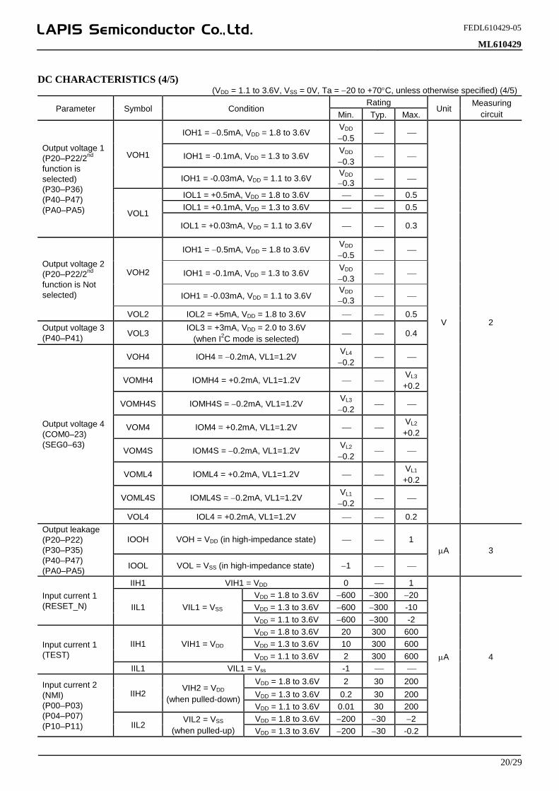
DC CHARACTERISTICS (4/5)
(VDD = 1.1 to 3.6V, VSS = 0V, Ta = −20 to +70°C, unless otherwise specified) (4/5)
Parameter Symbol Condition Rating
Unit Measuring
circuit Min. Typ. Max.
Output voltage 1 (P20–P22/2nd function is selected) (P30–P36) (P40–P47) (PA0–PA5)
VOH1
IOH1 = −0.5mA, VDD = 1.8 to 3.6V VDD
−0.5
V 2
IOH1 = -0.1mA, VDD = 1.3 to 3.6V VDD
−0.3
IOH1 = -0.03mA, VDD = 1.1 to 3.6V VDD −0.3
VOL1
IOL1 = +0.5mA, VDD = 1.8 to 3.6V 0.5 IOL1 = +0.1mA, VDD = 1.3 to 3.6V 0.5
IOL1 = +0.03mA, VDD = 1.1 to 3.6V 0.3
Output voltage 2 (P20–P22/2nd function is Not selected)
VOH2
IOH1 = −0.5mA, VDD = 1.8 to 3.6V VDD
−0.5
IOH1 = -0.1mA, VDD = 1.3 to 3.6V VDD
−0.3
IOH1 = -0.03mA, VDD = 1.1 to 3.6V VDD
−0.3
VOL2 IOL2 = +5mA, VDD = 1.8 to 3.6V 0.5 Output voltage 3 (P40–P41) VOL3
IOL3 = +3mA, VDD = 2.0 to 3.6V (when I2C mode is selected)
0.4
Output voltage 4 (COM0–23) (SEG0–63)
VOH4 IOH4 = −0.2mA, VL1=1.2V VL4
−0.2
VOMH4 IOMH4 = +0.2mA, VL1=1.2V VL3
+0.2
VOMH4S IOMH4S = −0.2mA, VL1=1.2V VL3
−0.2
VOM4 IOM4 = +0.2mA, VL1=1.2V VL2
+0.2
VOM4S IOM4S = −0.2mA, VL1=1.2V VL2
−0.2
VOML4 IOML4 = +0.2mA, VL1=1.2V VL1
+0.2
VOML4S IOML4S = −0.2mA, VL1=1.2V VL1
−0.2
VOL4 IOL4 = +0.2mA, VL1=1.2V 0.2 Output leakage (P20–P22) (P30–P35) (P40–P47) (PA0–PA5)
IOOH VOH = VDD (in high-impedance state) 1 µA 3
IOOL VOL = VSS (in high-impedance state) −1
Input current 1 (RESET_N)
IIH1 VIH1 = VDD 0 1
µA 4
IIL1 VIL1 = VSS VDD = 1.8 to 3.6V −600 −300 −20 VDD = 1.3 to 3.6V −600 −300 -10 VDD = 1.1 to 3.6V −600 −300 -2
Input current 1 (TEST)
IIH1 VIH1 = VDD VDD = 1.8 to 3.6V 20 300 600 VDD = 1.3 to 3.6V 10 300 600 VDD = 1.1 to 3.6V 2 300 600
IIL1 VIL1 = Vss -1
Input current 2 (NMI) (P00–P03) (P04–P07) (P10–P11)
IIH2 VIH2 = VDD
(when pulled-down)
VDD = 1.8 to 3.6V 2 30 200 VDD = 1.3 to 3.6V 0.2 30 200 VDD = 1.1 to 3.6V 0.01 30 200
IIL2 VIL2 = VSS
(when pulled-up) VDD = 1.8 to 3.6V −200 −30 −2 VDD = 1.3 to 3.6V −200 −30 -0.2
FEDL610429-05
ML610429
21/29
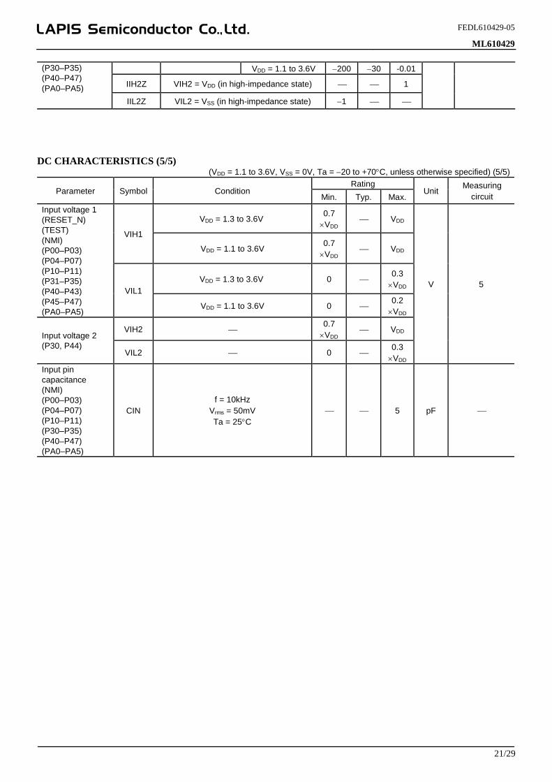
(P30–P35) (P40–P47) (PA0–PA5)
VDD = 1.1 to 3.6V −200 −30 -0.01
IIH2Z VIH2 = VDD (in high-impedance state) 1
IIL2Z VIL2 = VSS (in high-impedance state) −1
DC CHARACTERISTICS (5/5)
(VDD = 1.1 to 3.6V, VSS = 0V, Ta = −20 to +70°C, unless otherwise specified) (5/5)
Parameter Symbol Condition Rating
Unit Measuring
circuit Min. Typ. Max. Input voltage 1 (RESET_N) (TEST) (NMI) (P00–P03) (P04–P07) (P10–P11) (P31–P35) (P40–P43) (P45–P47) (PA0–PA5)
VIH1
VDD = 1.3 to 3.6V 0.7
×VDD VDD
V 5
VDD = 1.1 to 3.6V 0.7
×VDD VDD
VIL1 VDD = 1.3 to 3.6V 0
0.3 ×VDD
VDD = 1.1 to 3.6V 0 0.2
×VDD
Input voltage 2 (P30, P44)
VIH2 0.7
×VDD VDD
VIL2 0 0.3
×VDD Input pin capacitance (NMI) (P00–P03) (P04–P07) (P10–P11) (P30–P35) (P40–P47) (PA0–PA5)
CIN f = 10kHz
Vrms = 50mV Ta = 25°C
5 pF
FEDL610429-05
ML610429
22/29
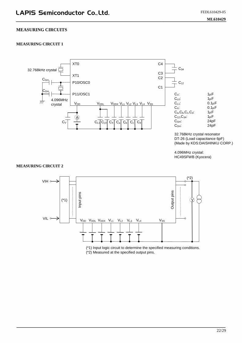
MEASURING CIRCUITS MEASURING CIRCUIT 1 MEASURING CIRCUIT 2
CV: 1µF CL0: 1µF CL1: 0.1µF CX: 0.1µF Ca,Cb,Cc,Cd: 1µF C12,C34: 1µF CGH: 24pF CDH: 24pF 32.768kHz crystal resonator DT-26 (Load capacitance 6pF) (Made by KDS:DAISHINKU CORP.) 4.096MHz crystal: HC49SFWB (Kyocera)
XT0
XT1
P10/OSC0
P11/OSC1
32.768kHz crystal
4.096MHz crystal
CGH
CDH
A
VDD VDDL VDDX
CL1 CL0 CX
VL1
Ca
VL2
Cb
VL3
Cc
VL4
Cd
VSS
C4
C3 C2
C1 C12
C34
CV
Inpu
t pin
s
V
VDD VDDL VDDX VL1 VL2 VL3 VL4 VSS
VIH
VIL
Out
put p
ins
(*1) Input logic circuit to determine the specified measuring conditions. (*2) Measured at the specified output pins.
(*2)
(*1)
FEDL610429-05
ML610429
23/29
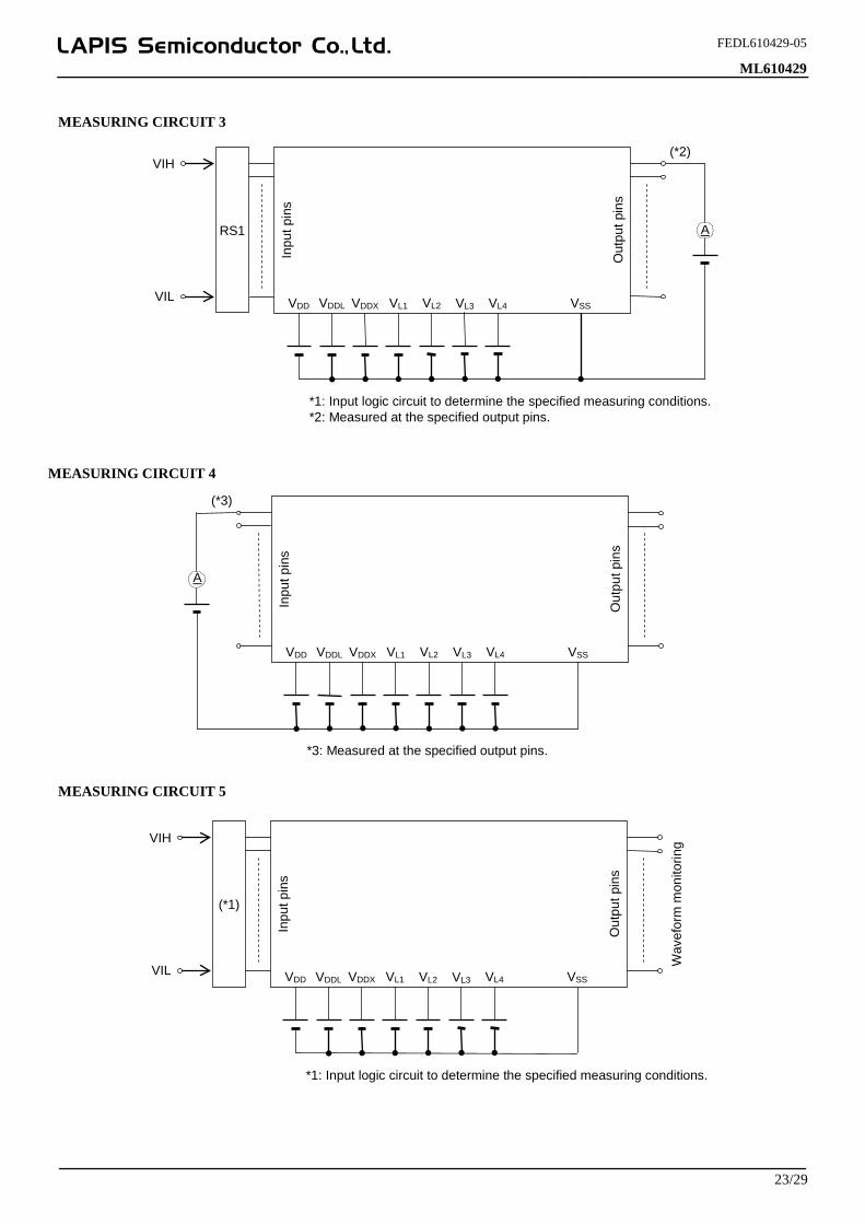
MEASURING CIRCUIT 3
MEASURING CIRCUIT 4 MEASURING CIRCUIT 5
Inpu
t pin
s
A
VDD VDDL VDDX VL1 VL2 VL3 VL4 VSS
VIH
VIL
Out
put p
ins
*1: Input logic circuit to determine the specified measuring conditions. *2: Measured at the specified output pins.
(*2)
RS1
Inpu
t pin
s
A
VDD VDDL VDDX VL1 VL2 VL3 VL4 VSS
Out
put p
ins
*3: Measured at the specified output pins.
(*3)
Inpu
t pin
s
VDD VDDL VDDX VL1 VL2 VL3 VL4 VSS
VIH
VIL
Out
put p
ins
*1: Input logic circuit to determine the specified measuring conditions.
(*1)
Wav
efor
m m
onito
ring
FEDL610429-05
ML610429
24/29
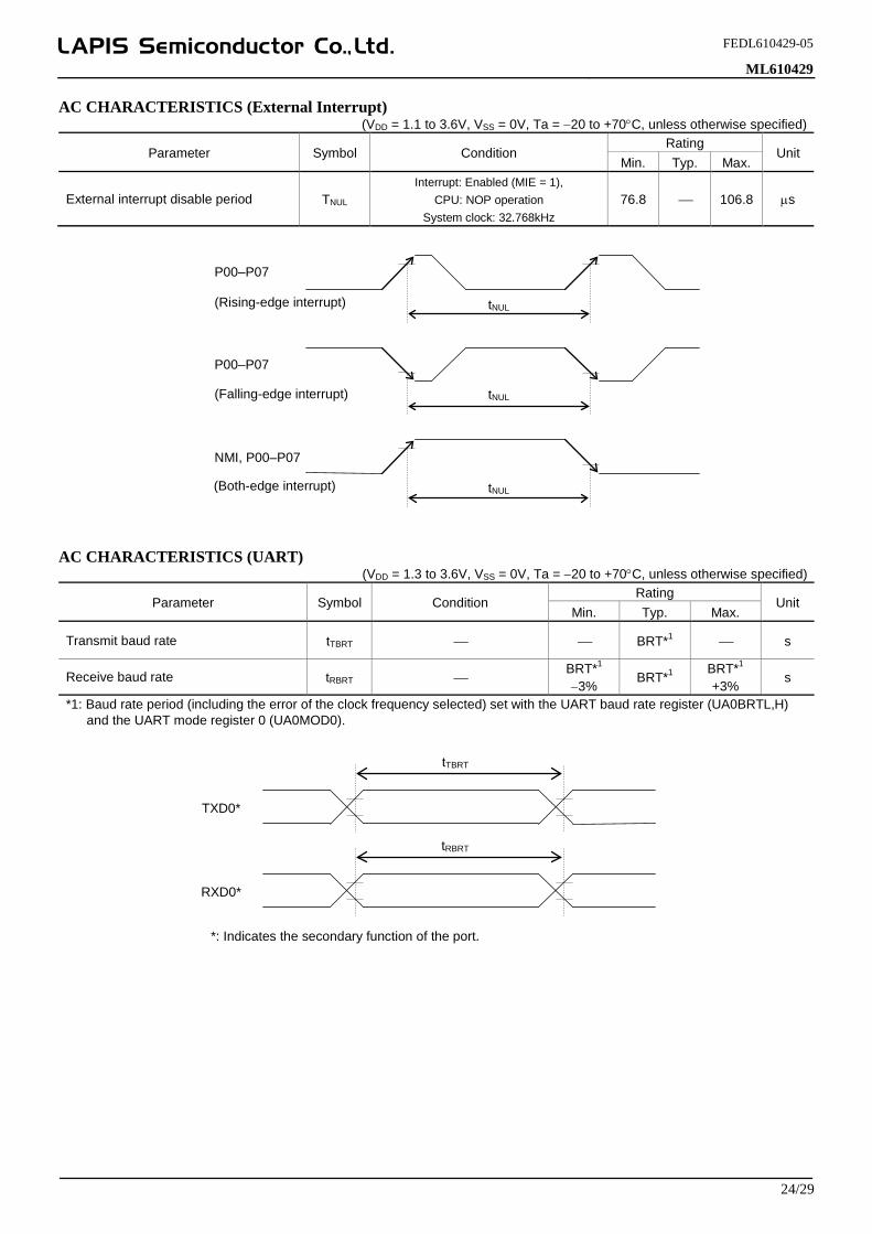
AC CHARACTERISTICS (External Interrupt) (VDD = 1.1 to 3.6V, VSS = 0V, Ta = −20 to +70°C, unless otherwise specified)
Parameter Symbol Condition Rating
Unit Min. Typ. Max.
External interrupt disable period TNUL Interrupt: Enabled (MIE = 1),
CPU: NOP operation System clock: 32.768kHz
76.8 106.8 µs
AC CHARACTERISTICS (UART)
(VDD = 1.3 to 3.6V, VSS = 0V, Ta = −20 to +70°C, unless otherwise specified)
Parameter Symbol Condition Rating
Unit Min. Typ. Max.
Transmit baud rate tTBRT BRT*1 s
Receive baud rate tRBRT BRT*1 −3%
BRT*1 BRT*1 +3%
s
*1: Baud rate period (including the error of the clock frequency selected) set with the UART baud rate register (UA0BRTL,H) and the UART mode register 0 (UA0MOD0).
tNUL
P00–P07
(Rising-edge interrupt)
P00–P07
(Falling-edge interrupt)
NMI, P00–P07
(Both-edge interrupt) tNUL
tNUL
tRBRT
TXD0*
RXD0*
*: Indicates the secondary function of the port.
tTBRT
FEDL610429-05
ML610429
25/29
AC CHARACTERISTICS (Synchronous Serial Port)
(VDD = 1.3 to 3.6V, VSS = 0V, Ta = −20 to +70°C, unless otherwise specified)
Parameter Symbol Condition Rating
Unit Min. Typ. Max.
SCLK input cycle (slave mode) tSCYC
When high-speed oscillation is not active
10 µs
When high-speed oscillation is active (VDD = 1.8 to 3.6V)
1 µs
SCLK output cycle (master mode) tSCYC SCLK*1 s
SCLK input pulse width (slave mode) tSW
When high-speed oscillation is not active
4 µs
When high-speed oscillation is active (VDD = 1.8 to 3.6V)
0.4 µs
SCLK output pulse width (master mode) tSW
SCLK*1 ×0.4
SCLK*1 ×0.5
SCLK*1 ×0.6
s
SOUT output delay time (slave mode) tSD
When high-speed oscillation is not active
540 ns
When high-speed oscillation is active (VDD = 1.8 to 3.6V)
240 ns
SOUT output delay time (master mode) tSD
When high-speed oscillation is not active
500 ns
When high-speed oscillation is active (VDD = 1.8 to 3.6V)
240 ns
SIN input setup time (slave mode)
tSS 80 ns
SIN input setup time (master mode)
tSS
When high-speed oscillation is not active
500 ns
When high-speed oscillation is active (VDD = 1.8 to 3.6V)
240 ns
SIN input hold time tSH
When high-speed oscillation is not active
300 ns
When high-speed oscillation is active (VDD = 1.8 to 3.6V)
80 ns
*1: Clock period selected with S0CK3–0 of the serial port 0 mode register (SIO0MOD1)
tSD
SCLK0*
SIN0*
SOUT0*
*: Indicates the secondary function of the port.
tSD
tSS tSH
tSW tSW
tSCYC
FEDL610429-05
ML610429
26/29
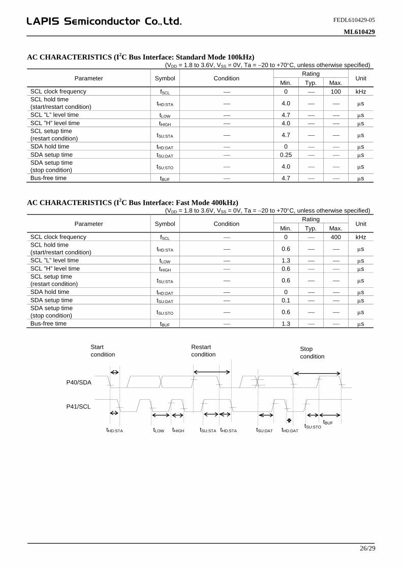
AC CHARACTERISTICS (I2C Bus Interface: Standard Mode 100kHz)
(VDD = 1.8 to 3.6V, VSS = 0V, Ta = −20 to +70°C, unless otherwise specified)
Parameter Symbol Condition Rating
Unit Min. Typ. Max.
SCL clock frequency fSCL 0 100 kHz SCL hold time (start/restart condition) tHD:STA 4.0 µs
SCL ”L” level time tLOW 4.7 µs SCL ”H” level time tHIGH 4.0 µs SCL setup time (restart condition) tSU:STA 4.7 µs
SDA hold time tHD:DAT 0 µs SDA setup time tSU:DAT 0.25 µs SDA setup time (stop condition) tSU:STO 4.0 µs
Bus-free time tBUF 4.7 µs AC CHARACTERISTICS (I2C Bus Interface: Fast Mode 400kHz)
(VDD = 1.8 to 3.6V, VSS = 0V, Ta = −20 to +70°C, unless otherwise specified)
Parameter Symbol Condition Rating
Unit Min. Typ. Max.
SCL clock frequency fSCL 0 400 kHz SCL hold time (start/restart condition) tHD:STA 0.6 µs
SCL ”L” level time tLOW 1.3 µs SCL ”H” level time tHIGH 0.6 µs SCL setup time (restart condition) tSU:STA 0.6 µs
SDA hold time tHD:DAT 0 µs SDA setup time tSU:DAT 0.1 µs SDA setup time (stop condition) tSU:STO 0.6 µs
Bus-free time tBUF 1.3 µs
P41/SCL
P40/SDA
Start condition
Restart condition
Stop condition
tBUF tHD:STA tLOW tHIGH tSU:STA tHD:STA tSU:DAT tHD:DAT tSU:STO
FEDL610429-05
ML610429
27/29
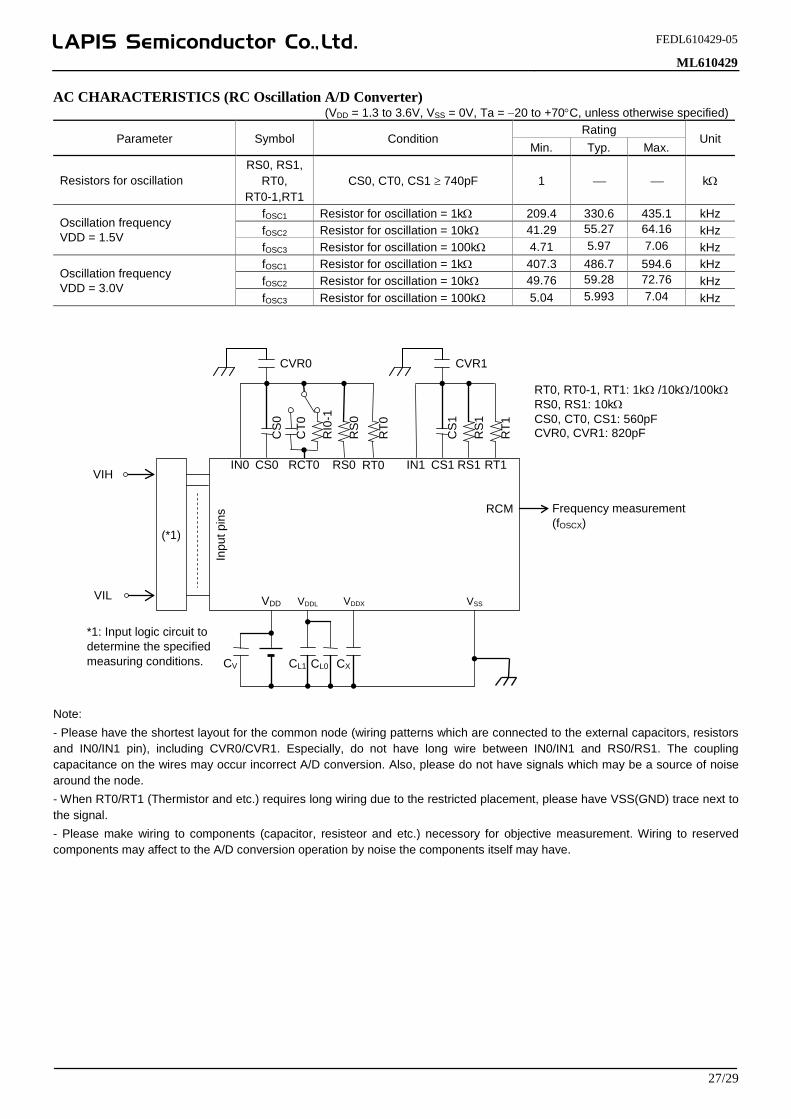
AC CHARACTERISTICS (RC Oscillation A/D Converter) (VDD = 1.3 to 3.6V, VSS = 0V, Ta = −20 to +70°C, unless otherwise specified)
Parameter Symbol Condition Rating
Unit Min. Typ. Max.
Resistors for oscillation RS0, RS1,
RT0, RT0-1,RT1
CS0, CT0, CS1 ≥ 740pF 1 kΩ
Oscillation frequency VDD = 1.5V
fOSC1 Resistor for oscillation = 1kΩ 209.4 330.6 435.1 kHz fOSC2 Resistor for oscillation = 10kΩ 41.29 55.27 64.16 kHz fOSC3 Resistor for oscillation = 100kΩ 4.71 5.97 7.06 kHz
Oscillation frequency VDD = 3.0V
fOSC1 Resistor for oscillation = 1kΩ 407.3 486.7 594.6 kHz fOSC2 Resistor for oscillation = 10kΩ 49.76 59.28 72.76 kHz fOSC3 Resistor for oscillation = 100kΩ 5.04 5.993 7.04 kHz
Note: - Please have the shortest layout for the common node (wiring patterns which are connected to the external capacitors, resistors and IN0/IN1 pin), including CVR0/CVR1. Especially, do not have long wire between IN0/IN1 and RS0/RS1. The coupling capacitance on the wires may occur incorrect A/D conversion. Also, please do not have signals which may be a source of noise around the node. - When RT0/RT1 (Thermistor and etc.) requires long wiring due to the restricted placement, please have VSS(GND) trace next to the signal. - Please make wiring to components (capacitor, resisteor and etc.) necessory for objective measurement. Wiring to reserved components may affect to the A/D conversion operation by noise the components itself may have.
VDD VDDL VDDX
CL1 CL0 CX
VSS
CV
RT0, RT0-1, RT1: 1kΩ /10kΩ/100kΩ RS0, RS1: 10kΩ CS0, CT0, CS1: 560pF CVR0, CVR1: 820pF
RCM Frequency measurement (fOSCX)
Inpu
t pin
s
VIH
VIL
*1: Input logic circuit to determine the specified measuring conditions.
(*1)
CS0 RT0
IN1 CS1 RS1 RT1
CS
0
RS0
RS
0
RCT0
RI0
-1
CT0
RT0
CS
1
RS
1
RT1
IN0
CVR0 CVR1
FEDL610429-05
ML610429
28/29
Revision History
Document No. Date Page
Description Previous Edition
Current Edition
FEDL610428-01 Sep.9.2011 – – Formally edition 1.0
FEDL610428-02 Dec.22.2011 30 30 Change the AC Characteristics (RC Oscillation A/D Converter)
FEDL610428-03 Jul.3.2012 30 30 Change the AC Characteristics (RC Oscillation A/D Converter)
FEDL610428-04 Jul.25.2014
All All Change header and footer 3 3 Delete the metal option of only ML610429’s LCD driver
3 4 Change from "Shipment" to " Product name – Supported Function "
- 21 Add CLOCK GENERATION CIRCUIT OPERATING CONDITIONS
20 22 Change "RESET" to "Reset pulse width (PRST)" and " Power-on reset activation power rise time (TPOR )".
22 24 Correct the CGL’s value and the CDL’s value of DC CHARACTERISTICS (3/5)’s note No.3
31 33 Update Package Dimensions
FEDL610428-05 Apr.24.2015
All All Change header and footer 1~5 7~9
11~15 17~19
1~3 6~10
12~13 Delete ML610428
33 - Delete ML610429 Package
2 2 Corrected a typo. “100kbps@1MHz HSCLK” is corrected to 100kbps@4MHz HSCLK.
FEDL610429-05
ML610429
29/29
Notes 1) The information contained herein is subject to change without notice. 2) Although LAPIS Semiconductor is continuously working to improve product reliability and quality, semiconductors can
break down and malfunction due to various factors. Therefore, in order to prevent personal injury or fire arising from failure, please take safety measures such as complying with the derating characteristics, implementing redundant and fire prevention designs, and utilizing backups and fail-safe procedures. LAPIS Semiconductor shall have no responsibility for any damages arising out of the use of our Products beyond the rating specified by LAPIS Semiconductor.
3) Examples of application circuits, circuit constants and any other information contained herein are provided only to illustrate
the standard usage and operations of the Products.The peripheral conditions must be taken into account when designing circuits for mass production.
4) The technical information specified herein is intended only to show the typical functions of the Products and examples of
application circuits for the Products. No license, expressly or implied, is granted hereby under any intellectual property rights or other rights of LAPIS Semiconductor or any third party with respect to the information contained in this document; therefore LAPIS Semiconductor shall have no responsibility whatsoever for any dispute, concerning such rights owned by third parties, arising out of the use of such technical information.
5) The Products are intended for use in general electronic equipment (i.e. AV/OA devices, communication, consumer systems,
gaming/entertainment sets) as well as the applications indicated in this document.
6) The Products specified in this document are not designed to be radiation tolerant.
7) For use of our Products in applications requiring a high degree of reliability (as exemplified below), please contact and consult with a LAPIS Semiconductor representative: transportation equipment (i.e. cars, ships, trains), primary communication equipment, traffic lights, fire/crime prevention, safety equipment, medical systems, servers, solar cells, and power transmission systems.
8) Do not use our Products in applications requiring extremely high reliability, such as aerospace equipment, nuclear power
control systems, and submarine repeaters.
9) LAPIS Semiconductor shall have no responsibility for any damages or injury arising from non-compliance with the recommended usage conditions and specifications contained herein.
10) LAPIS Semiconductor has used reasonable care to ensure the accuracy of the information contained in this document.
However, LAPIS Semiconductor does not warrant that such information is error-free and LAPIS Semiconductor shall have no responsibility for any damages arising from any inaccuracy or misprint of such information.
11) Please use the Products in accordance with any applicable environmental laws and regulations, such as the RoHS Directive.
For more details, including RoHS compatibility, please contact a ROHM sales office. LAPIS Semiconductor shall have no responsibility for any damages or losses resulting non-compliance with any applicable laws or regulations.
12) When providing our Products and technologies contained in this document to other countries, you must abide by the
procedures and provisions stipulated in all applicable export laws and regulations, including without limitation the US Export Administration Regulations and the Foreign Exchange and Foreign Trade Act.
13) This document, in part or in whole, may not be reprinted or reproduced without prior consent of LAPIS Semiconductor.
Copyright 2011 – 2015 LAPIS Semiconductor Co., Ltd.
2-4-8 Shinyokohama, Kouhoku-ku,
Yokohama 222-8575, Japan http://www.lapis-semi.com/en/