the msu miniball 4π fragment detection array
TRANSCRIPT
Nuclear Instruments and Methods in Physics Research A295 (1990) 109-122North-Holland
The
SLJ Miniba1141T fragment detection arrayR.T. De Souza, N. Carlin *, Y.D. Kim, J. Ottarson, L. Phair, D.R. Bowman,C.K. Gelbke, W.G. Gong, W.G. Lynch, R.A. Pelak * *, T. Peterson +, G. PoggiM.B. Tsang and H.M. XuNational Superconducting Cyclotron Laboratory and Department of Physics andAstronomy, Michigan State University,East Lansing, MI 48824, USA
Received 30 March 1990
A compact and highly granular charged particle detection array, covering 89% of 41T in solid angle, is described . In its presentconfiguration, the array consists of 188 fast-plastic CsI(Tl) phoswich detectors arranged in 11 rings coaxial about the beam axis . Eachphoswich detector is comprised of a 40 Rm. thick plastic scintillator foil and a 2 cm thick CsI(Tl) crystal selected for good scintillationuniformity. The detectors are read out by photomultiplier tubes . Elemental identification up to Z =18 and isotopic identification ofH and He nuclei is achieved by exploiting pulse shape discrimination techniques.
1 . Introduction
Highly excited nuclear systems, formed in inter-mediate and high-energy nuclear reactions, can decayby emitting a considerable number of complex frag-ments [1] . Such multifragment emission processes are ofparticular interest, since they might provide importantinformation about the liquid-gas phase diagram ofnuclear matter [2,3] . At sufficiently high excitation en-ergies, the internal pressure in the nuclear mediumcould be large enough to cause an expansion . If, duringthis expansion phase, the reaction trajectory in thetemperature-density plane passes through the spinodalline, the system could become mechanically unstableagainst the growth of density fluctuations and decay bya multifragment disintegration [4-9] . Experimental evi-dence concerning the existence and characterization of amultifragment decay mode is still rather limited . Inorder to study multiple emission off complex fragmentswith nearly 4% coverage, we have constructed a frag-ment detection array of high granularity and low detec-tion thresholds. In its present configuration, the devicecovers
a-n angun.vtaaala ." r~wnnbvu off
- 0 0
1 %Îl 0 ..,;*l~. 1 QQcoveas dacu a
vislab - i -ivar
v.aua avv
Present address: Instituto de Física, Universidade de SäoPaulo, C. Postal 20516, CEP 01498, Sio Paulo, Brazil .Present address : Department of Physics, Cornell Univer-sity, Ithaca, NY 14853, USA.Present address : Department of Physics, GustavusAdolphus College, Saint Peter, MN 56082, USA .Permanent address : Dipartimento di Fisica dell'Universitàand INFN, Largo Enrico Fermi 2, 50125 Firenze, Italy .
0168-9002/90/$03 .50 © 1990 - Elsevier Science Publishers B.V. (North-Holland)
2. Mechanical construction of the array
109
phoswich detectors consisting of 40 Wm thick plasticscintillator foils and 2 cm thick CsI(Tl) scintillators.Thresholds for particle identification range from E/A=1.5 MeV for alpha particles to E/A = 3 MeV for Caions. Individual detectors can resolve elements fromZ = 1-18, as well as isotopes of hydrogen and helium .Charged particle detector arrays based on similar tech-niques have been described in refs. [10,11] .
In this paper, we give a detailed description of thedevice and its performance characteristics. The mecha-nical construction of the array is described in section 2.In sections 3-6, the detector design, the photomultipliergain monitoring system, quality tests of CsI(Tl) crystals,and the technique for the fabrication of uniform thinscintillator foils will be presented . The data acquisitionelectronics and test results for particle identification willbe detailed in sections 7 and 8. A brief summary will begiven in section 9 .
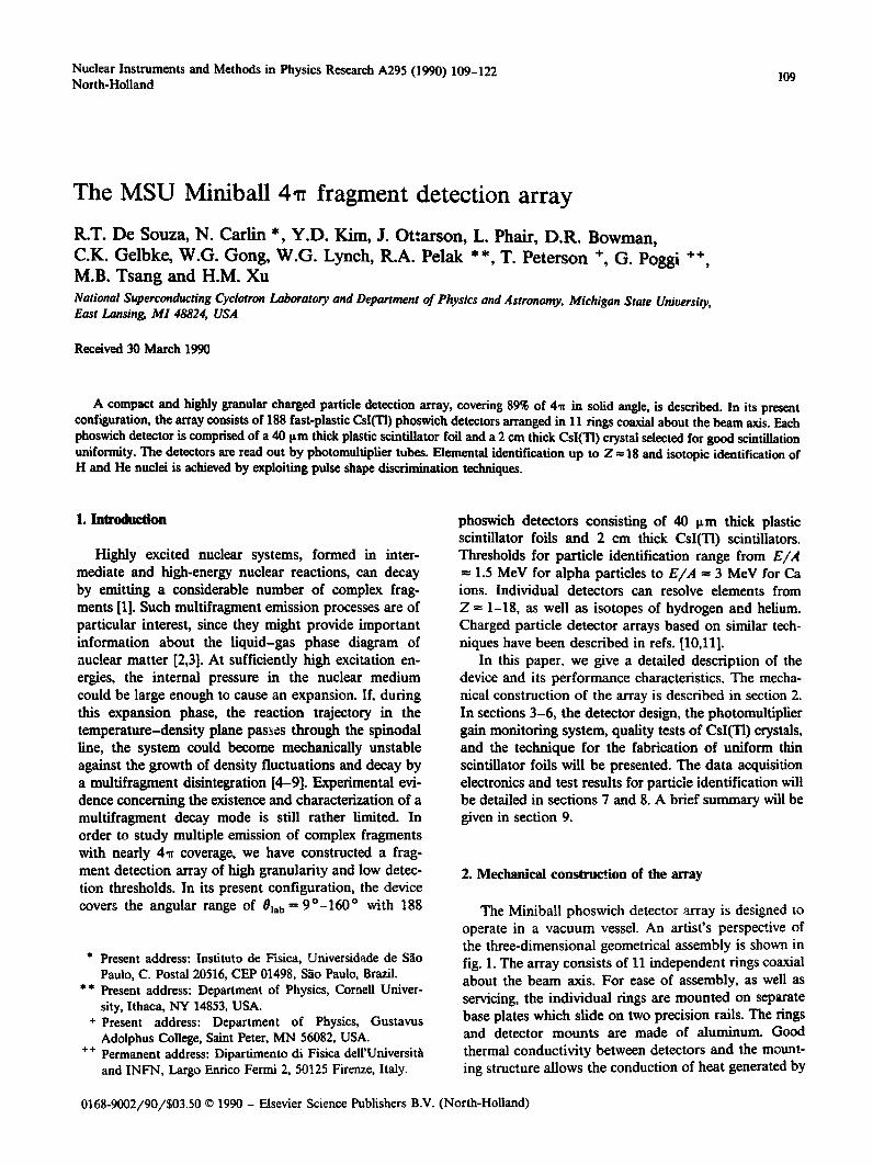
1'he Miniball phoswich detector array is designed tooperate in a vacuum vessel . An artist's perspective ofthe three-dimensional geometrical assembly is shown infig. l . The array consists of 11 independent rings coaxialabout the beam axis . For ease of assembly, as well asservicing, the individual rings are mounted on separatebase plates which slide on two precision rails . The ringsand detector mounts are made of aluminum . Goodthermal conductivity between detectors and the mount-ing structure allows the conduction of heat generated by
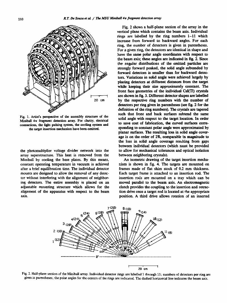
Fig. 1. Artist's perspective of the assembly structure of theMiniball 4ar fragment detection array. For clarity, electricalconnections, the light pulsing system, the cooling system and
the target insertion mechanism have been omitted.
the photomultiplier voltage divider network into thearray superstructure . This heat is removed from theMiniball by cooling the base plates . By this means,constant operating temperature in vacuum is achievedafter a brief equilibration time . The individual detectormounts are designed to allow the removal of any detec-tor without interfering with the alignment of neighbor-ing detectors. The entire assembly is placed on anadjustable mounting structure which allows for thealignment of the apparatus with respect to the beamaxis.
RT. De Soma et al. / TheMSUMiniball 41r fragment detection array
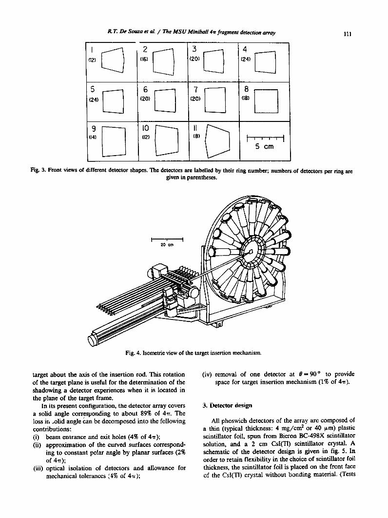
Fig. 2 shows a half-plane section of the array in thevertical plane which contains the beam axis . Individualrings are labelled by the ring numbers 1-11 whichincrease from forward to backward angles. For eachring, the number of detectors is given in parentheses.For a given ring, the detectors are identical in shape andhave the same polar angle coordinates with respect tothe beam axis; these angles are indicated in rig. 2. Sincethe angular distributions of the emitted particles arestrongly forward peaked, the solid angle subtended byforward detectors is smaller than for backward detec-tors. Variations in solid angle were achieved largely byplacing detectors at different distances from the targetwhile keeping their size approximately constant. Thefront face geometries of the individual CsI(Tl) crystalsare shown in fig. 3. Different detector shapes are labelledby the respective ring numbers with the number ofdetectors per ring given in parentheses (see fig. 2 for thedefinition of the ring numbers). The crystals are taperedsuch that front and back surfaces subtend the samesolid angle with respect to the target location . In orderto save cost of fabrication, the curved surfaces corre-sponding to constant polar angle were approximated byplanar surfaces. The resulting loss in solid angle cover-age is on the order of 2%, comparable in magnitude tothe loss in solid angle coverage resulting from gapsbetween individual detectors (which :bust be providedto allow for mechanical tolerances and optical isolationbetween neighboring crystals).
An isometric drawing of the target insertion mecha-nism is shown in fig . 4. The targets are mounted onframes made of flat shim stock of 0.2 mm thickness .Each target frame is attached to an insertion rod. Theinsertion rods are mounted on a tray which can bemoved parallel to the beam axis. An electromagneticclutch provides the coupling to the insertion and retrac-tion drive once a target rod is located at the appropriateposition . A third drive allows rotation of an inserted
20 cmFig. 2 . Half-plane section of the Miniball array. Individual detector rings are labelled 1 through 11 ; numbers of detectors per ring aregiven in parentheses; the polar angles for the centers of the rings are indicated. The dashed horizontal line indicates the beam axis.
RT. De Souza et al. / The MSUMiniball 4w fragment detection array
Fig. 3 . Front views of different detector shapes. The detectors are labelled by their ring number ; numbers .of detectors per ring aregiven in parentheses.
target about the axis of the insertion rod . This rotationof the target plane is useful for the determination of theshadowing a detector experiences when it is located inthe plane of the target frame .
In its present configuration, the detector array coversa solid angle corresponding to about 89% of 41T . Theloss in olid angle can be decomposed into the followingcontributions :(i)beamentrance and exit holes (4% of 41T) ;(ii) approximation of the curved surfaces correspond-
ing to constant polar angle by planar surfaces (2%of 4,Yr ) ;
(iii) optical isolation of detectors and allowance formechanical tolerances ;4% of 4%) ;
Fig . 4 . Isometric view of the target insertion mechanism.
3. Detector design
(iv) removal of one detector at 8 = 90 °
to providespace for target insertion mechanism (1% of 41T).
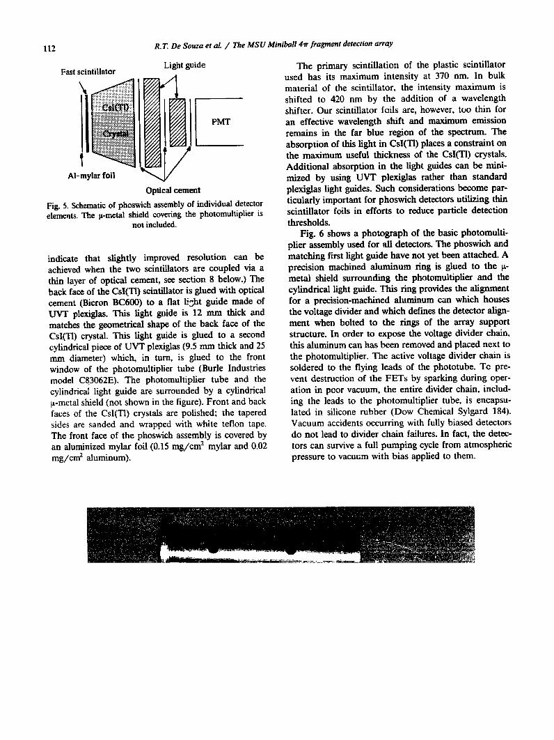
All phoswich detectors of the array are composed ofa thin (typical thickness : 4 mg/cm2 or 40 pm) plasticscintillator foil, spun from Bicron BC-498X scintillatorsolution, and a 2 cm CsI(T1) scintillator crystal . Aschematic of the detector design is given in fig . 5 . Inorder to retain flexibility in the choice of scintillator foilthickness, the scintillator foil is placed on the front faceof the Csl(Tl) crystal without bonding material . (Tests
I 2 3 4(12) Cl (t6) (20) (24)
5 6 7 8(24) (20) (20) tl8)
9 10 II(14) (12) (8)
5 cm
RT. De Souza et al. / TheMSUMiniba!! 4v fragment detection array
Optical cement
Fig. 5. Schematic of phoswich assembly of individual detectorelements. The p-metal shield covering the photomultiplier is
not included.
indicate that slightly improved resolution can be
achieved when the two scintillators are coupled via a
thin layer of optical cement, see section 8 below.) The
back face of the CsI(TI) scintillator is glued with optical
cement (Bicron BC600) to a flat L;ht guide made ofUVT plexiglas. This light guide is 12 mm thick andmatches the geometrical shape of the back face of theCsI(TI) crystal. This light guide is glued to a secondcylindrical piece of UVT plexiglas (9 .5 mm thick and 25mm diameter) which, in turn, is glued to the frontwindow of the photomultiplier tube (Burle Industriesmodel C83062E). The photomultiplier tube and thecylindrical light guide are surrounded by a cylindrical[L-metal shield (not shown in the figure). Front and backfaces of the CsI(Tl) crystals are polished ; the taperedsides are sanded and wrapped with white teflon tape.The front face of the phoswich assembly is covered byan aluminized mylar foil (0.15 mg/crrr mylar and 0.02mg/cm2 aluminum).
The primary scintillation of the plastic scintillatorused has its maximum intensity at 370 nm. In bulkmaterial of the scintillator, the intensity maximum isshifted to 420 nm by the addition of a wavelengthshifter. Our scintillator foils are, however, too thin foran effective wavelength shift and maximum emissionremains in the far blue region of the spectrum. Theabsorption of this light in CsI(Tl) places a constraint onthe maximum useful thickness of the CsI(TI) crystals .Additional absorption in the light guides can be mini-mized by using UVT plexiglas rather than standardplexiglas light guides . Such considerations become par-ticularly important for phoswich detectors utilizing thinscintillator foils in efforts to reduce particle detectionthresholds .
Fig. 6 shows a photograph of the basic photomulti-plier assembly used for all detectors. The phoswich andmatching first light guide have not yet been attached . Aprecision machined aluminum ring is glued to the Wmetal shield surrounding the photomultiplier and thecylindrical light guide. This ring provides the alignmentfor a precision-machined aluminum can which housesthe voltage divider and which defines the detector align-ment when bolted to the rings of the array supportstructure. In order to expose the voltage divider chain,this aluminum can has been removed and placed next tothe photomultiplier. The active voltage divider chain issoldered to the flying leads of the phototube. Tc pre-vent destruction of the FETs by sparking during oper-ation in poor vacuum, the entire divider chain, includ-ing the leads to the photomultiplier tube, is encapsu-lated in silicone rubber (Dow Chemical Sylgard 184) .Vacuum accidents occurring with fully biased detectorsdo not lead to divider chain failures . In fact, the detec-tors can survive a full pumping cycle from atmosphericpressure to vacuum with bias applied to them.
CABLE
-110MS2
10MÁ
'_MR
3.9 Mn
3.9 M a
68okn
680ka
680 kSl
IMR
680kll
1 .8 Ma SHV CABLE_ _
-HV
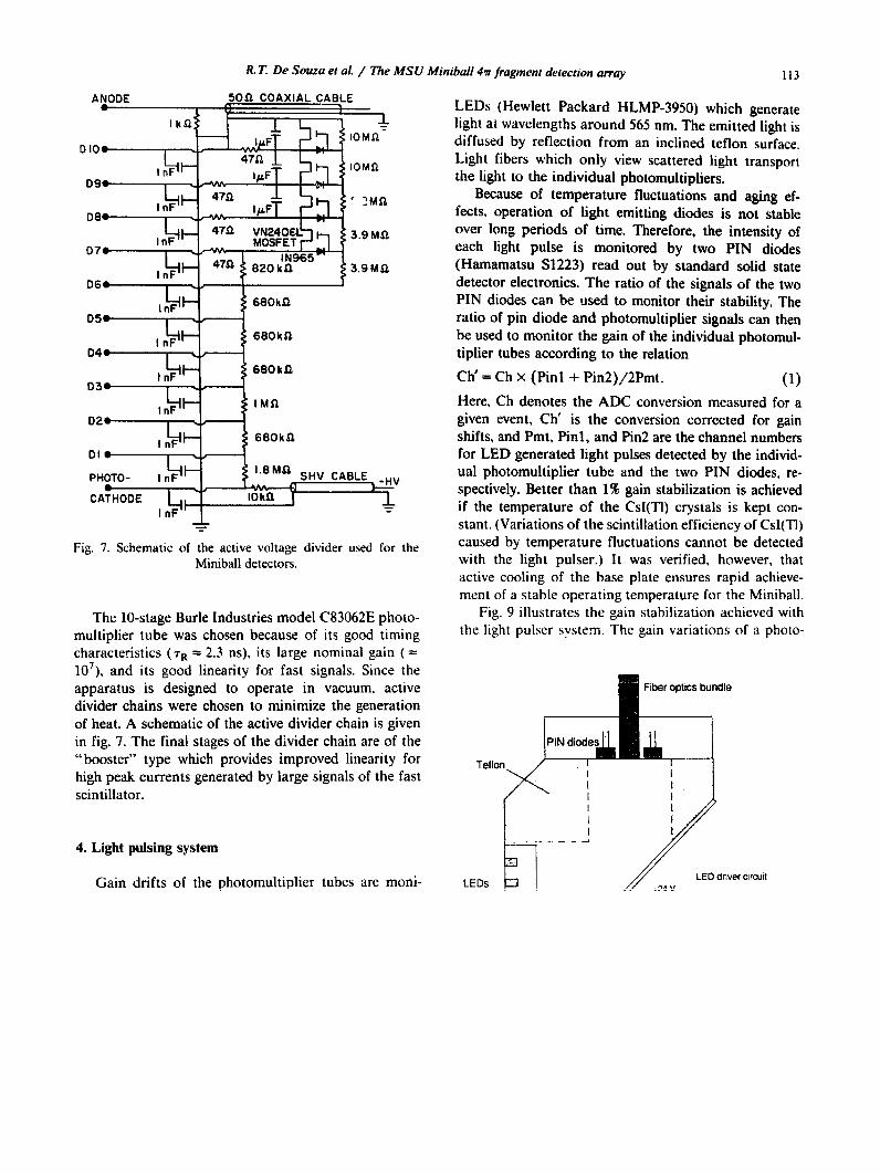
Fig . 7 . Schematic of the active voltage divider used for theMiniball detectors.
The 10-stage Burle Industries model C83062E photo-multiplier tube was chosen because of its good timingcharacteristics (TR = 2.3 ns), its large nominal gain107 ), and its good linearity for fast signals . Since theapparatus is designed to operate in vacuum, activedivider chains were chosen to minimize the generationof heat. A schematic of the active divider chain is givenin fig. 7 . The final stages of the divider chain are of the"booster" type which provides improved linearity forhigh peak currents generated by large signals of the fastscintillator .
4 . Light pulsing system
Gain drifts of the photomultiplier tubes are moni-
/ The MSU Miniba!! 4-ff fragment detection array
LEDs (Hewlett Packard HLMP-3950) which generatelight at wavelengths around 565 nm . The emitted light isdiffused by reflection from an inclined teflon surface .Light fibers which only view scattered light transportthe light to the individual photomultipliers.
Because of temperature fluctuations and aging ef-fects, operation of light emitting diodes is not stableover long periods of time . Therefore, the intensity ofeach light pulse is monitored by two PIN diodes(Hamamatsu S1223) read out by standard solid statedetector electronics. The ratio of the signals of the twoPIN diodes can be used to monitor their stability. Theratio of pin diode and photomultiplier signals can thenbe used to monitor the gain of the individual photomul-tiplier tubes according to the relationCh' = Ch x (Pinl + Pin2)/2Pmt .Here, Ch denotes the ADC conversion measured for agiven event, Ch' is the conversion corrected for gainshifts, and Pmt, Pinl, and Pin2 are the channel numbersfor LED generated light pulses detected by the individ-ual photomultiplier tube and the two PIN diodes, re-spectively . Better than 1% gain stabilization is achievedif the temperature of the CsI(TI) crystals is kept con-stant . (Variations of the scintillation efficiency of CsI(Tl)caused by temperature fluctuations cannot be detectedwith the light pulser .) It was verified, however, thatactive cooling of the base plate ensures rapid achieve-ment of a stable operating temperature for the Miniball .
Fig . 9 illustrates the gain stabilization achieved withthe light pulser system . The gain variations of a photo-
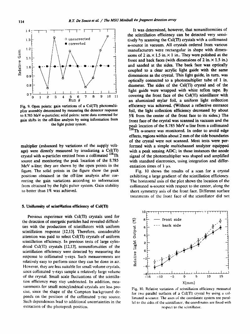
R. T. De Souzza et al. / The MSU Miniball 4w fragment detection array
Fig . 9. Open points: gain variations of a CsI(TI) photomulti-plier assembly determined by measuring the detector responseto 8.785 MeV a-particles; solid points : same data corrected forgain shifts in the off-line analysis by using information from
the light pulser system.
multiplier (enhanced by variations of the supply volt-age) were directly measured by irradiating a CsI(TI)crystal with a-particles emitted from a collimated 228Thsource and monitoring the peak location of the 8.785MeV a-line ; they are shown by the open points in thefigure . The solid points in the figure show the peakpositions obtained in the off-line analysis after cor-recting the gain variations according to informationfrom obtained by the light pulser system . Gain stabilityto better than 1 % was achieved.
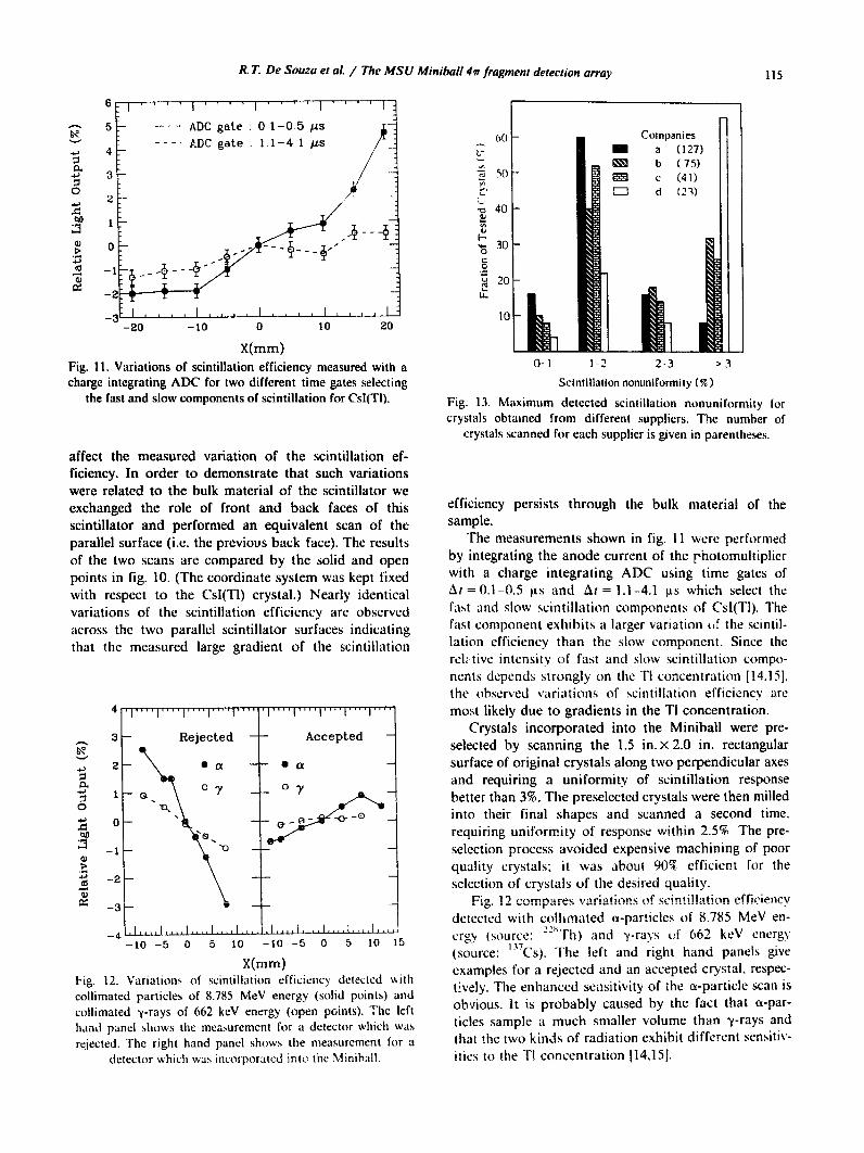
5. Uniformity of scintillation efficiency of CsifI7)
Previous experience with Csl(TI) crystals used forthe detection of energetic particles had revealed difficul-ties with the production of scintillators with uniformscintillation response [12,131 . Therefore, considerableattention was paid to select CsI(Tl) crystals of uniformscintillation efficiency. In previous tests of large cylin-drical CsI(Tl) crystals [12,131, nonunifort,tities of thescintillation efficiency were detected by measuring theresponse to collimated -y-rays. Such measurements arerelatively easy to perform since they can be done in air .However, they are less suitable for small volume crystals,since collimated -y-rays sample a relatively large volumeof the crystal . Small scale fluctuations of the scintilla-tion efficiency may stay undetected . In addition, mea-surements for small noncylindrical crystals are less pre-cise, since the shape of the Compton background de-pends on the position of the collimated -y-ray source .Such dependences lead to additional uncertainties in theextraction of the photopeak position .
It was determined, however, that nonuniformities ofthe scintillation efficiency can be detected very sensi-tively by scanning the CsI(TI) crystals with a collimateda-source in vacuum . All crystals ordered from variousmanufacturers were rectangular in shape with dimen-sions of 2 in . x 1 .5 in. x 1 in . . They were polished at thefront and back faces (with dimensions of 2 in . x 1 .5 in .)and sanded at the sides. The back face was opticallycoupled to a clear acrylic light guide with the samedimensions as the crystal. This light guide, in turn, wasoptically connected to a photomultiplier tube of 1 in .diameter. The sides of the CsI('I1) crystal and of thelight guide were wrapped with white teflon tape . Bycovering the front face of the CsI(T1) scintillator withan aluminized mylar foil, a uniform light collectionefficiency was achieved . (Without a reflective entrancefoil, the light collection efficiency decreased by about5% from the center of the front face to its sides.) Thefront face of the crystal was scanned in vacuum and thepeak location of the 8.785 MeV a-line from a collimated28Th a-source was monitored . In order to avoid edge
effects, regions within about 2 mm of the side boundariesof the crystal were not scanned . Most tests were per-formed with a simple multichannel analyzer equippedwith a peak sensing ADC; in those instances the anodesignal of the photomultiplier was shaped and amplifiedwith standard electronics, using integration and differ-entiation times of 1 gs .
Fig . 10 shows the results of a scan for a crystalexhibiting a large gradient of the scintillation efficiency .The horizontal axis of the plot shows the location of thecollimated a-source with respect to the center, along theshort symmetry axis of the front face . Different surfacetreatments of the front face of the scintillator did not
X(mm)Fig. 10. Relative variation of scintillation efficiency measuredfor two parallel surfaces of a Csl(TI) crystal by using a col-limated a-source . The axes of the coordinate system are parallel to the sides of the scintillator ; the coordinates are fixed with
respect to the scintillator .
0
X(mm)Fig. 11 . Variations of scintillation efficiency measured with acharge integrating ADC for two different time gates selecting
the fast and slow components of scintillation for Csl(TI).
affect the measured variation of the scintillation ef-ficiency . In order to demonstrate that such variationswere related to the bulk material of the scintillator weexchanged the role of front and back faces of thisscintillator and performed an equivalent scan of theparallel surface (i .e . the previous back face) . The resultsof the two scans are compared by the solid and openpoints in fig . 10 . (The coordinate system was kept fixedwith respect to the Csl(TI) crystal .) Nearly identicalvariations of the scintillation efficiency are observedacross the two parallel scintillator surfaces indicatingthat the measured large gradient of the scintillation
4
3
2
ffi
-4 W1.11.L11.11
-10 -5
R. T. De Souza et al. / TheMSUMiniba!! 41r fragment detection array
F-r-IT- -̀*-rT`-T,-,-I,--`-1
Accepted
0 5 10 -10 -5 0 5 10 15
X(mm)Fig. 12 . Variations of scintillation efficiency detected withcollimated particles of 8.785 MeV energy (solid points) andcollimated -y-rays of 662 keV energy (open points). The lefthand panel shows the measurement for a detector which wasrejected . The right hand panel shows the measurement for a
detector which was incorporated into the Miniball .
60
V14J
30óCnro 20LL
10
0-1
1-2
2-3
> 3
Scintillation nonuniformity (%)
Fig. 13 . Maximum detected scintillation nonuniformity forcrystals obtained from different suppliers . The number of
crystals scanned for each supplier is given in parentheses .
efficiency persists through the bulk material of thesample .
The measurements shown in fig . 11 were performedby integrating the anode current of the photomultiplierwith a charge integrating ADC using time gates ofAt = 0.1-0.5 fts and ®t = 1 .1-4.1 p,s which select thefast and slow scintillation components of Csl(TI) . Thefast component exhibits a larger variation of the scintil-lation efficiency than the slow component . Since therely Live intensitv of fast and slow scintillation compo-nents depends strongly on the Tl concentration [14 .15],the observed variations of scintillation efficiency aremost likely due to gradients in the TI concentration .
Crystals incorporated into the Miniball were pre-selected by scanning the 1 .5 in . x 2.0 in . rectangularsurface of original crystals along two perpendicular axesand requiring a uniformity of scintillation responsebetter than 3% . The preselected crystals were then milledinto their final shapes and scanned a second time,requiring uniformity of response within 2.5% . The pre-selection process avoided expensive machining of poorquality crystals ; it was about 90% efficient for theselection of crystals of the desired quality .
Pin 12 onmnnrrrc unrintinn of srintillminn effiriençv.a.r .- .detected with collimated oc-particles of 8.785 MeV en-ergy (source : ""Th) and y-rays of 662 keV energy(source : ' z'Cs) . The left and right hand panels giveexamples for a rejected and an accepted crystal, respec-tively . The enhanced sensitivity of the ot-particle scan isobvious . It is probably caused by the fact that «-par-ticles sample a much smaller volume than -y-rays andthat the two kinds of radiation exhibit different sensitiv-ities to the TI concentration [14,15] .
The results of our standardized prescans are dis-played in fig . 13 . The histogram shows the number ofscanned crystals, obtained from different companies, asa function of maximum detected scintillation uniform-ity. Crystals obtained from one supplier (a) were grownwith the Czochralski technique [16,17] ; crystals ob-tained from three other suppliers (b)-(d) were grownwith the Stockbarger-Bridgman technique [17,18] .Crystals grown with the Czochralski technique ex-hibited, on average, more uniform scintillation efficien-cies than crystals grown with the Stockbarger-Bridg-man technique. Quality differences between differentsuppliers using the Stockbarger-Bridgman techniquemay not be significant since only a limited number ofcrystals were scanned for each supplier. (The number ofcrystals scanned from each supplier is given inparentheses in fig . 13 .) Furthermore, some differencesare expected to result from different ways of cutting the2 in. x 1.5 in . x 1 in . crystals from the ingot, since TIconcentration gradients build up largely in the verticalcrystal growth direction . Our standard scan of the 1.5in . x 2.0 in . face of each crystal should then reveal anespecially large gradient of the scintillation efficiencywhen the 2 in . long side was cut parallel to the verticalgrowth direction of the ingot . Selective cuts of somecrystals from various locations of the ingot and withdifferent orientations with respect to the crystal growthdirection provided supporting evidence for the relation-ship between the In concentration and the uniformity ofscintillation response. For most of the crystals, suchdetailed information was not available to us .
6. Fabrication of scintillator foils
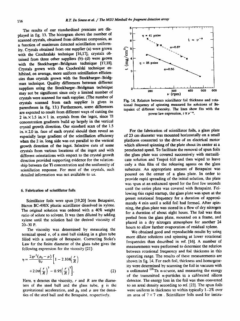
Scintillator foils were spun [19,20] from Betapaint,Bicron BC-498X plastic scintillator dissolved in xylene.The original solution was ordered with a 400 weightratio of solute to solvent . It was then diluted by addingxylene until the solution had the desired viscosity of20-30 P.
The viscosity was determined by measuring theterminal speed v, of a steel ball sinking in a glass tubefilled with a sample of Betapaint . Correcting Stoke'sLaw for the finite diameter of the glass tube gives thefnlln�;,no PvnrPCC;nn fnr th,- v;crnc;tv r'?11 "avaav..aaab vr~t.ravvvavaa fo . wav .avvvv~ .) L---1 .
RT. De Souaa et al. / TheMSUMiniball 4w fragment detection array
2gr2(9o - p)
1-2.104(-9 )
r+2.Oy(
rR )3 - 0.95(r
)SI .
(2)Here, q denotes the viscosity, r and R are the diame-ters of the steel ball and the glass tube, g is thegravitational acceleration, and po and p are the densi-ties of the steel ball and the Betapaint, respectively .
e7
6
cv 5
2
t « v-«
200
300 400 500 600v (rpm)
Fig. 14. Relation between scintillator foil thickness and rota-tional frequency of spinning measured for solutions of Betapaint of different viscosity . The lines show fits with the
power law expression, t a v- °.
For the fabrication of scintillator foils, a glass plateof 23 cm diameter was mounted horizontally on a smallplatform connected to the drive of an electrical motorwhich allowed spinning of the plate about its center at apreselected speed . To facilitate the removal of spun foilsthe glass plate was covered successively with metasili-cate solution and Teepol 610 and then wiped to leaveonly a thin film of the releasing agents on the glasssubstrate . An appropriate amount of Betapaint waspoured on the center of a glass plate . In order toprovide rapid spreading o ¬ the initial solution, the platewas spun at an enhanced speed for the first few secondsuntil the entire plate was covered with Betapaint . Fol-lowing this rapid startup, the glass plate was spun at thepreset rotational frequency for a duration of approxi-mately 4 min until a solid foil had formed . After spin-ning, the glass plate was stored in a flow of dry nitrogenfor a duration of about eight hours . The foil was thenpeeled from the glass plate, mounted on a frame, andplaced in a dry nitrogen atmosphere for another 24hours to allow further evaporation of residual xylene .We obtained good and reproducible results by using
more dilute solutions and spinning at lower rotationalfrequencies than described in ref. [16] . A number ofmeasurements were performed to determine the relationbetween rotational frequency and foil thickness in thisoperating range . The results of these measurements areshown in fig. 14 . For each foil, thickness and homogene-ity were determined by scanning the foil in vacuum witha collimated 228Th a-scurce, and measuring the energyof the transmitted a-particles in a calibrated silicondetector . The energy loss in the foil was then convertedto an areal density according to ref . [22] . The spun foilswere uniform in thickness to within typically 1-2% overan area of 7 x 7 cm . Scintillator foils used for instru-
cw
0
a0á
roa>x
4
GLUED o
fast plastic2
0
-4-
6-
4
WRAPPED
fast plastic2
--- Csl0-
-2r-4
R.T. De Souza
position
et al. / The MSU Miniball 4v fragment detection array
1
I
I
I
I
I
I
I
I
I
I0 1 2 3 4 5 6 7 a 9 10 11 12
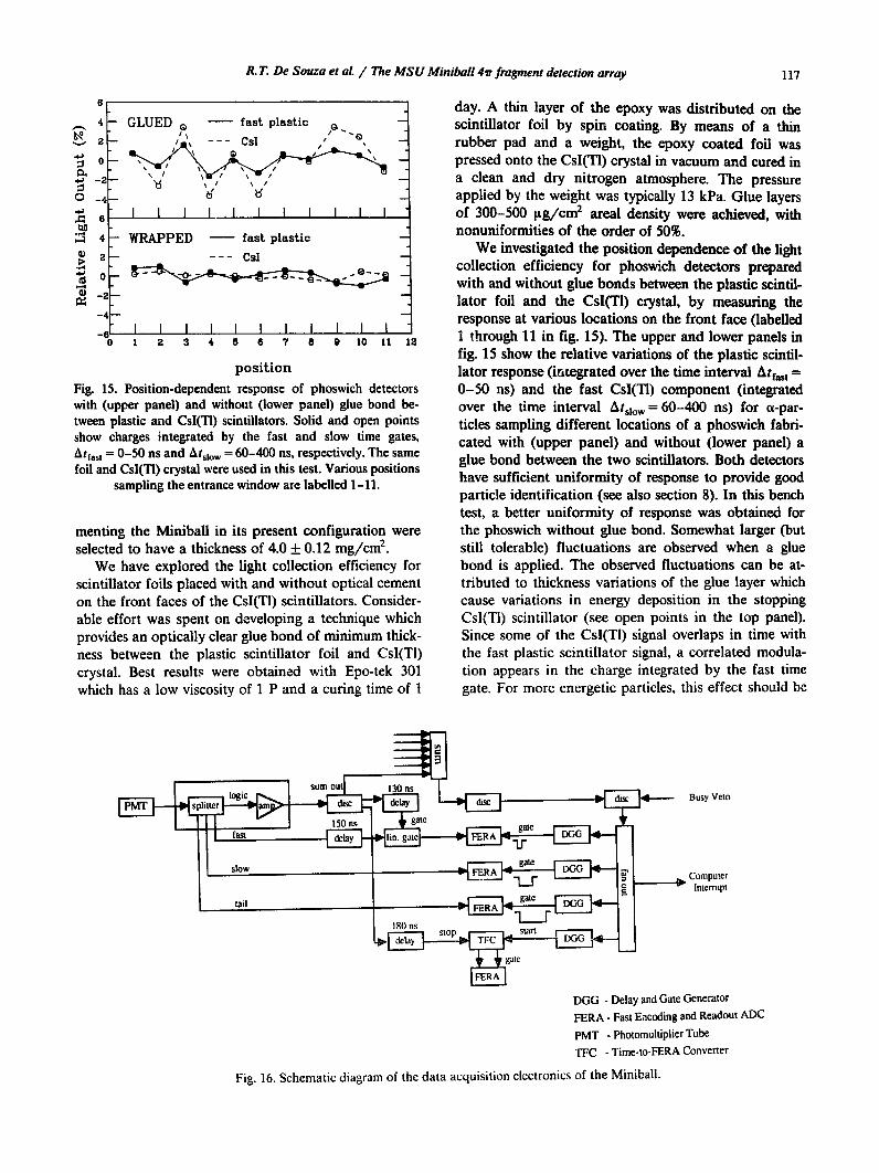
Fig. 15 . Position-dependent response of phoswich detectorswith (upper panel) and without (lower panel) glue bond be-tween plastic and Csl(Tl) scintillators. Solid and open pointsshow charges integrated by the fast and slow time gates,Atfas, = 0-50 ns and At .,.,, = 60-400 ns, respectively . The samefoil and CsI(T1) crystal were used in this test . Various positions
sampling the entrance window are labelled 1-11 .
menting the Miniball in its present configuration wereselected to have a thickness of 4.0 ± 0.12 mg/cm2 .We have explored the light collection efficiency for
scintillator foils placed with and without optical cementon the front faces of the CsI(T1) scintillators. Consider-able effort was spent on developing a technique whichprovides an optically clear glue bond of minimum thick-ness between the plastic scintillator foil and Csl(TI)crystal . Best results were obtained with Epo-tek 301which has a low viscosity of 1 P and a curing time of 1
day . A thin layer of the epoxy was distributed on thescintillator foil by spin coating . By means of a thinrubber pad and a weight, the epoxy coated foil waspressed onto the CsI(TI) crystal in vacuum and cured ina clean and dry nitrogen atmosphere. The pressureapplied by the weight was typically 13 kPa. Glue layersof 300-500 Rg/cm2 areal density were achieved, withnonuniformities of the order of 50`6.We investigated the position dependence of the light
collection efficiency for phoswich detectors preparedwith and without glue bonds between the plastic scintil-lator foil and the CsI(Tl) crystal, by measuring theresponse at various locations on the front face (labelled1 through 11 in fig. 15) . The upper and lower panels infig. 15 show the relative variations of the plastic scintil-lator response (integrated over the time interval Atfast =0-50 ns) and the fast CsI(Tl) component (integratedover the time interval At st .W = 60-400 ns) for a-par-ticles sampling different locations of a phoswich fabri-cated with (upper panel) and without (lower panel) aglue bond between the two scintillators. Both detectorshave sufficient uniformity of response to provide goodparticle identification (see also section 8). In this benchtest, a better uniformity of response was obtained forthe phoswich without glue bond . Somewhat larger (butstill tolerable) fluctuations are observed when a gluebond is applied . The observed fluctuations can be at-tributed to thickness variations of the glue layer whichcause variations in energy deposition in the stoppingCsl(TI) scintillator (see open points in the top panel).Since some of the CsI(Tl) signal overlaps in time withthe fast plastic scintillator signal, a correlated modula-tion appears in the charge integrated by the fast timegate . For more energetic particles, this effect should be
Fig . 16 . Schematic diagram of the data acquisition electronics of the Miniball.
DGG - Delay and Gate GeneratorFERA - Fast Encoding and Readout ADCPMT - PhotomultiplierTubeTFC - Time-to-FERA Converter
a
R.T. De Souza et al. / TheMSUMiniball 4ffragment detection array
.. ...
.w . . í 1li .. .: " e"
n
SLOW
't
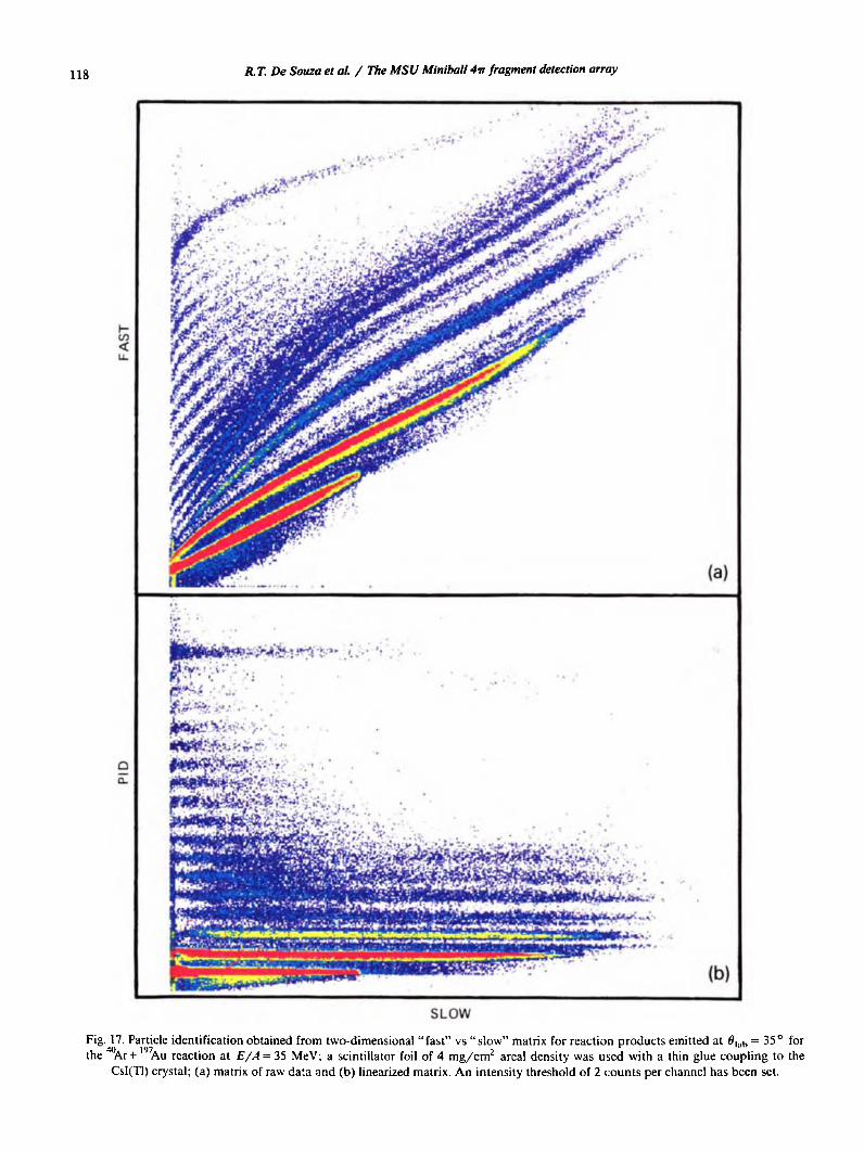
Fig. 17. Particle identification obtained from two-dimensional "fast" vs "slow" matrix for reaction products emitted at B,�b = 35' forthe 4°Ar+ 197Au reaction at E/A = 35 MeV; a scintillator foil of 4 mg/cm2 areal density was used with a thin glue coupling to the
Csl(Tl) crystal ; (a) matrix of raw data and (b) linearized matrix . An intensity threshold of 2 counts per channel has been set .
7. Data acquisition electronics
R.T. De Souza et al. / The MSUMiniball 4wfragment detection array
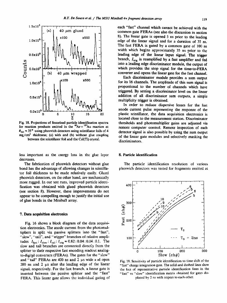
10 15 20Z
Fig. 18. Projections of linearized particle identification spectrafor reaction products emitted in the °°Ar+197Au reaction atBlab - 35° using phoswich detectors using scintillator foils of 4mg/cm2 thickness; (a) with and (b) without glue coupling
between the scintillator foil and the Csl(TI) crystal.
less important as the energy loss in the glue layerdecreases .
The fabrication of phoswich detectors without gluebond has the advantage of allowing changes in scintilla-tor foil thickness to be made relatively easily . Gluedphoswich detectors, on the other hand, are mechanicallymore rugged. In our test runs, improved particle identi-fication was obtained with glued phoswich detectors(see section 8). However, these improvements do notappear to be compelling enough to justify the initial useof glue bonds in the Miniball array.
Fig. 16 shows a block diagram of the data acquisi-tion electronics. The anode current from the photomul-tipliers is split via passive splitters into the "fast","slow", '-tail", and "trigger" branches or relative ampli-tudes Ifast : Istow : Itail : Itrig '`` 0.82 :0.04 :0.04 :0 .1 . Theslow and tail branches are connected directly from thesplitter to their respective fast encoding readout analog-to-digitLl converters (FERAs). The gates for the "slow"and "tail" FERAs are 400 ns and 2 lts wide aA open200 ns and 2 lts after the leading edge of the linearsignal, respectively. For the fast branch, a linear gate isinserted between the passive splitter and the "fast"FERA . This linear gate allows the individual gating of
each "fast" channel which cannot be achieved with thecommon gate FERAs (see also the discussion in section8). The linear gate is opened 5 ns prior to the leadingedge of the linear signal and for a duration of 35 ns.The fast FERA is gated by a common gate of 100 nswidth which begins approximately 35 ns prior to theleading edge of the linear input signal. The triggerbranch, Itri g is reamplified by a fast amplifier and fedinto a leading edge discriminator module, the output ofwhich provides the stop signal for the time-to-FERAconverter and opens the linear gate for the fast channel.
Each discriminator module provides a sum outputfor its 16 channels . The amplitude of this sum signal isproportional to the number of channels which havetriggered. By setting a discriminator level on the linearaddition of all discriminator sum outputs, a simplemultiplicity trigger is obtained .
In order to reduce dispersive losses for the fastanode current pulse representing the response of theplastic scintillator, the data acquisition electronics islocated close to the measurement station . Discriminatorthresholds and photomultiplier gains are adjusted viaremote computer control . Remote inspection of eachdetector signal is also possible by using the sum outputof the linear gate modules and selectively masking thediscriminators .
8. Particle identification
The particle identification resolution of variousphoswich detectors was tested for fragments emitted at
400
300
co 200
100
Fig. 19. Sensitivity of particle identification to time shift of the"fast" charge integration gate . The solid and dashed lines showthe loci of representative particle identification lines in the"fast" vs "slow" identification matrix obtained for gates dis-
placed by 2 ns with respect to each other.
120
about e1ab= 35 ° in the 4°Ar + 197Au reaction at E/A =
35 MeV. All data were taken with the standard electron-ics setup described in the previous section. Fig. 17ashows a two-dimensional plot of the fast versus the slowcharge integration parameters for a phoswich consistingof a 4 mg/cm? scintillator foil glued to the CsI(Tl)crystal. Elemental identification up to Z =18 is achievedover a considerable dynamical range of particle en-ergies . Fig. 17b shows a linearized presentation of thesedata which is more suitable to display the resolution of
RT. De Souza et al. / TheMSUMiniball 4w fragment detection array
. c
the device. From such a linearized presentation, projec-tions on the particle identification axis can be generatedwhich show the particle identification resolution in amore quantitative form .
Spectra projected on the particle identification axisare shown in fig . 18 . Fig. 18a shows the projection ofthe data displayed in fig . 17 ; part (b) shows the resultfor a phoswich using a4 mg/cm2 scintillator foil withoutglue bond . Better resolution is obtained by using a gluebond between the scintillator foil and the CsI(Tl) crystal.
v
SLOW
rrr
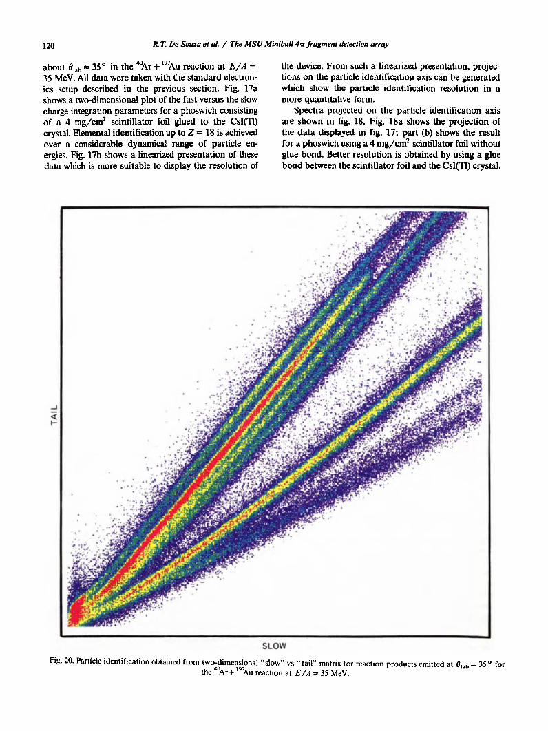
Fig. 20 . Particle identification obtained from two-dimensional "slow" vs "tail" matrix for reaction products emitted at 01ab = 35 ° forthe 4°Ar + 19'Au reaction at E/A = 35 MeV.
Additional improvements in particle identification reso-lution can be achieved by increasing the thickness of thescintillator foil . For a specific experiment, the benefitsof improved particle identification resolution due to anincrease in scintillator foil thickness must be weighedagainst the ensuing higher energy threshold. We havealso explored the use of thinner foils and found that theresolution deteriorates rapidly for scintillator foilsthinner than 3 mg/cm2. For most purposes, particleidentification provided by foils of 4 mg/cm2 thicknessis satisfactory.
The use of thin scintillator foils in phoswich detec-tors for particle identification is complicated by the factthat the fast plastic scintillator signal is superimposedon the rising signal from the CsI(TI) scintillator . Goodparticle identification via direct charge integration de-pends critically on well defined integration times . Elec-tronic walk introduced by leading edge discriminatorschanges the detailed shape of a particle identificationline in the fast versus slow matrix, but it has only minoreffects on the separation between adjacent particle iden-tification lines . Time jitter in the integration gate, how-ever, does have an adverse effect on the particle identifi-cation resolution, since it produces fluctuations in theamount of CsI(TI) scintillation integrated by the fasttime gate. If the fast component is integrated by ADCswith a common gate mode, loss in resolution will occurwhenever there is a time jitter between gates providedby different channels. Loss in resolution will be inevita-ble when more than two detected particles with differ-ent flight times are converted in separate channels of acommon gate ADC. The problem can be avoided byintroducing linear gates into the fast channel which areindividually opened (see fig . 16) or, alternatively, byemploying passive filter networks of good quality [23] .
Fig. 19 illustrates the sensitivity of the particle iden-tification to time jitter in the integration gate for thefast channel. The solid curves correspond to the centersof selected particle identification lines in the fast versusslow matrix (see, e.g . fig . 17) . The dashed curves showhow these particle identification lines are shifted whenthe gate of the fast ADC arrives 2 ns later in time . (Inthese two measurements, the gate width was kept con-stant.) Even a 2 ns time jitter in the fast gate is suffi-cient to mix the particle identification lines of neighbor-ina elements in the fast versus slow matrix .vIdentification of hydrogen and helium isotopes is
obtained by standard pulse shape discrimination tech-niques which make use of the fact that the temporaldecay of the Csl(Tl) light output depends on the ioniza-tion density of the detected particles [24-26] . As anexample, fig . 20 shows the particle identification ob-tained from a two-dimensional matrix of the slow versustail parameters . Good particle identification is obtainedover a broad range of energies. In these spectra, not allparticles are stopped in the CsI(TI) crystal. The effects
R.T. De Souza et al. / TheMSUMiniball 41r fragment detection array
of particles "punching through" the detectors are clearlyvisible . Particles not stopped in the Csl(T1) crystal canstill be separated by atomic number.
9. Summary
We have constructed a compact phoswich detectorarray for the detection of multifragment emission fromhighly excited nuclear systems in heavy ion inducedreactions . The array is designed to operate in vacuum. Itconsists of 188 individual phoswich detectors arrangedin 11 rings coaxial with the beam axis. The granularityof the device increases towards more forward angles.Each phoswich detector consists of a 4 mg/cm2 (40 Rm)thick plastic scintillator foil and a 2 cm thick CsI(Tl)crystal . By selecting Csl(TI) crystals of good scintilla-tion uniformity and homogenous scintillator foils, andby making efforts to preserve and cleanly integrate thefast anode signal containing the plastic scintillator re-sponse, good element identification up to Z =18 wasobtained . Detectors utilizing a thin glue bond betweenthe plastic scintillator foil and Csl(TI) crystal gaveslightly better particle identification resolution than de-tectors without glue bonds. However, since glue bondsincrease the energy threshold and make changes ofscintillator foil thickness very time and labor intensive,the argument for glued phoswich detectors does notappear compelling.
Acknowledgements
We wish to thank D.G . Sarantites, L.G . Sobotka, D.Swan, J. Telfer, and J . Yurkon for helpful discussions .Advice from M. Maier and J . Vincent on electronicsquestions is gratefully acknowledged . The continuedsupport from the entire NSCL staff and the excellentwork of the NSCL mechanical workshop are highlyappreciated . This work is based upon work supportedby the National Science Foundation under Grant num-bers PHY-86-11210 and PHY-89-13813 . W.G.L.acknowledge s the receipt of US Presidential YoungInvestigator Award and N.C . acknowledges partial sup-port by the FAPESP, Brazil.
eferences
[1] W.G . Lynch, Ann . Rev . Nucl . Part . Sci . 3 7 (1987) 493 andreferences contained therein .
[2] J.E. Finn, S . Agarwal, A. Bujak, J . Chuang, L.J. Gutay,A.S . Hirsch, R.W . Minich, N.T. Porile, R.P. Scharenberg,B.C . Stringfellow and F . Turkot, Phys . Rev . Lett . 49(1982) 1321 .
[3J L.P . Csernai and J .I . Kapusta, Phys . Rep . 131 (1986) 223 .
122
[4] G. Bertsch and P.J. Siemens, Phys . Lett. B126 (1983) 9.[5] J.A. Lopez and P.J . Siemens, Nucl. Phys. A431(1984) 728.[6] A. Vicentini, G. Jacucci and V.R . Pandharipande, Phys.
Rev. C31 (1985) 1783 .[7] R.J . Lenk and V.R . Pandharipande, Phys. Rev. C34 (1986)
177.[8] T.J. Schlagel and V.R . Pandharipande, Phys . Rev. (1987)
162.[9] K. Sneppen and L. Vinet, Nucl . Phys . A480 (1988) 342.
[10] D.G. Sarantites, L.G. Sobotka, T.M . Semkow, V. Abe-nante, J. Elson, J.T. Hood, Z. Li, N.G . Nicolis, D.W .Stracener, J. Valdes and D.C. Hensley, Nucl . Instr. andMeth . A264 (1988) 319.
[11] D. Drain et al ., Nucl. Instr. and Meth ., to be published.[12] W.G . Gong, Y.D. Kim, G. Poggi, Z. Chen, C.K . Gelbke,W.G . Lynch, M.R. Maier, T. Murakami, M.B. Tsang,H.M. Xu and K. Kwiatkowski, Nucl . Instr. and Meth .A268 (1988) 190.
[13] W.G. Gong,N. Carlin, C.K. Gelbke and R. Dayton, Nucl .Instr. and Meth . A287 (1990) 639.
[14] J.B. Birks, The Theory and Practice of ScinitllationCounting (Pergamon Press, New York, 1964) p. 92.
[15] W.W. Managan, IRE Trans. Nucl. Sci. NS-9 (3) (1962) 8.
RT. De Souza et al. / The MSU Miniball 41r fragment detection array
[16] J. Czochralski, Z. Phys . Chem . 92 (1918) 219.[17] J.C. Brice, The Growth of Crystals fron . `ie Melt (North
Holland, Amsterdam 1965).[18] P.W . Bridgman, Proc. Ana,-.r. Acad. Arts . Sci . 60 (1925)
305.[19] D. Meyerhofer, J. Appl . Phys. 49 (1978) 399 .[20] E. Norbeck, T.P. Dubbs and L.G . Sobotka, Nucl. Instr.
and Meth . A262 (1987) 564.[21] A. Dinsdale and F. Moore, Viscosity and its Measurement
(Chapman-Hill, London, 1962).[22] U. Littmark and J.F. Ziegler, Handbook of Range Distri-
butions for Energetic Ions in All Elements, vol. 6 of TheStopping and Ranges of Ions in Matter, ed . J.F . Ziegler(Pergamon, New York, 1980).
[23] D.G. Sarantites and L.G. Sobotka, private communica-tion .
[24] R.S. Storey, W. Jack and A. Ward, Proc. Phys . Soc. 72(1958) 1 .
[25] J.A . Biggerstaff, R.L . Becker and M.T. McEllistrem, Nucl.Instr. and Meth . 10 (1961) 327.
[26] J. Alarja, A. Dauchy, A. Giorni, C. Morand, E. Pollaco, P.Stassi, B. Billerey, B. Chambon, B. Cheynis, D. Drain andC. Pastor, Nucl . Instr. and Meth . A242 (1986) 352.