today modeling, design, and optimization effects lec 12
TRANSCRIPT
1
ESE370: Circuit-Level Modeling, Design, and Optimization for Digital Systems
Lec 12: October 5, 2016 Scaling
Penn ESE 370 Fall 2016 - Khanna
Today
! VLSI Scaling Trends/Disciplines ! Effects ! Alternatives (cheating)
Penn ESE 370 Fall 2016 - Khanna 2
Scaling
! Premise: features scale “uniformly” " everything gets better in a predictable manner
! Parameters: # λ (lambda) -- Mead and Conway (Day14) # F -- Half pitch – ITRS (F=2λ) # S – scale factor – Rabaey
# F’=S×F
Penn ESE 370 Fall 2016 - Khanna 3
ITRS Roadmap
! International Technology Roadmap for Semiconductors " Try to predict where industry going
! ITRS 2.0 started in 2015 with new focus " System Integration, Heterogeneous Integration,
Heterogeneous Components, Outside System Connectiviy, More Moore, Beyond CMOS and Factory Integartion.
! http://www.itrs2.net/
Penn ESE 370 Fall 2016 - Khanna 4
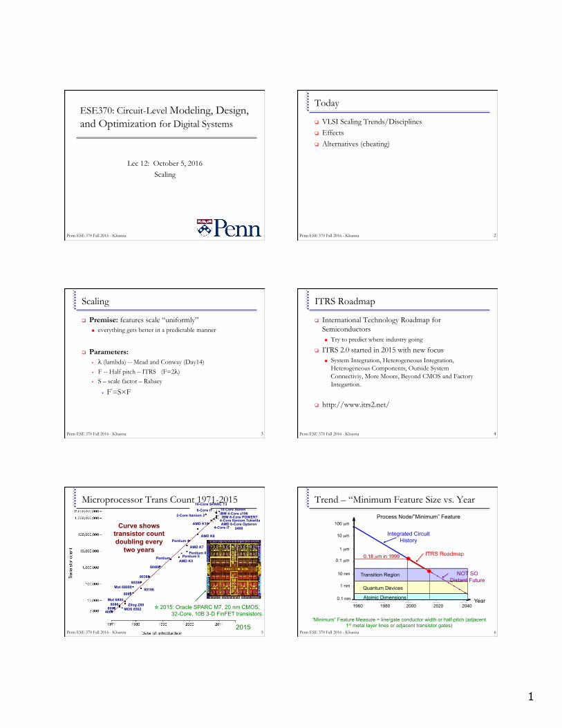
Microprocessor Trans Count 1971-2015
5 Kenneth R. Laker, University of Pennsylvania, updated 20Jan15
Curve shows transistor count doubling every
two years Pentium
4004 8006
8080 Mot 6800
8086
Mot 68000 80286
80386
80486
MOS 6502 Zilog Z80
80186
AMD K5 Pentium II
Pentium III AMD K7
Pentium 4 AMD K8
AMD K10 AMD 6-Core Opteron 2400 4-Core i7
2-Core Itanium 2 6-Core i7 6-Core i7 16-Core SPARC T3
10-Core Xenon IBM 4-Core z196 IBM 8-Core POWER7
4-Core Itanium Tukwilla
2015: Oracle SPARC M7, 20 nm CMOS, 32-Core, 10B 3-D FinFET transistors.
2015 Penn ESE 370 Fall 2016 - Khanna
Trend – “Minimum Feature Size vs. Year
6
Process Node/”Minimum” Feature
Year 1960 1980 2000 2020 2040
100 µm
10 µm
1 µm
0.1 µm
10 nm
1 nm
0.1 nm
Integrated Circuit History
0.18 µm in 1999 ITRS Roadmap
Transition Region
Quantum Devices
Atomic Dimensions
“Minimum” Feature Measure = line/gate conductor width or half-pitch (adjacent 1st metal layer lines or adjacent transistor gates)
Penn ESE 370 Fall 2016 - Khanna
NOT SO Distant Future

2
Intel Cost Scaling
7
http://www.anandtech.com/show/8367/intels-14nm-technology-in-detail
Penn ESE 370 Fall 2016 - Khanna
Moore’s Law Impact on Intel uComputers
8 2010 YEAR
Serial data links operating at 10 Gbits/sec.
Increased reuse of logic IP, i.e. designs and cores.
2BT µP (Intel Itanium Tukwila) 4-Core chip (65 nm) introduced Q1 2010.
3BT mP (Intel Itanium Poulson) 8-Core chip (32 nm) to be introduced 2012.
Introduces 22 nm Tri-gate Transistor Tech.
Complexity - # transistors Double every Two Years 0.022um
2011
0.032um 2009
Min Feature
Size
Penn ESE 370 Fall 2016 - Khanna
More-than-Moore
9
“More-than-Moore”, International Road Map (IRC) White Paper, 2011.
International Technology Road Map for Semiconductors
Scal
ing
Penn ESE 370 Fall 2016 - Khanna
More Moore $ Scaling
! Geometrical Scaling " continued shrinking of horizontal and vertical physical
feature sizes
! Equivalent Scaling " 3-dimensional device structure improvements and new
materials that affect the electrical performance of the chip even if no geometrical scaling
! Design Equivalent Scaling " design technologies that enable high performance, low
power, high reliability, low cost, and high design productivity even if neither geometrical nor equivalent scaling can be used
10 Penn ESE 370 Fall 2016 - Khanna
22nm 3D FinFET Transistor
11
Tri-Gate transistors with multiple fins connected together
increases total drive strength for higher performance
http://download.intel.com/newsroom/kits/22nm/pdfs/22nm-Details_Presentation.pdf
High-k gate
dielectric
Penn ESE 370 Fall 2016 - Khanna
More Moore $ Scaling
! Examples: " Design-for-variability " Low power design (sleep modes, clock gating, multi-
Vdd, etc.) " Multi-core SOC architectures
12 Penn ESE 370 Fall 2016 - Khanna

3
Semiconductor System Integration – More Than Moore's Law
13
1010
109
108
107
106
105
104
103
102
10
Transistors/cm2
1010
109
108
107
106
105
104
103
102
10
Com
ponents/cm2
1970 1980 1990 2000 2010 2020
Multichip Module
System- in-package
(SIP) System-
on-package (SOP)
R. Tummala, “Moore's Law Meets Its Match”, IEEE Spectrum, June, 2006
SOP law for system integration. As components shrink and boards all but disappear, component density will double every year or so.
Penn ESE 370 Fall 2016 - Khanna
Improvement Trends for VLSI SoCs Enabled by Geometrical and Equivalent Scaling
! TRENDS: ! Higher Integration level
" exponentially increased number of components/transistors per chip/package.
! Performance Scaling " combination of Geometrical
(shrinking of dimensions) and Equivalent (innovation) Scaling.
! System implementation " SoC + increased use of SiP -
> SOP
! CONSEQUENCES: ! Higher Speed
" CPU clock rate at multiple GHz + parallel processing.
! Increased Compactness & less weight " increasing
system integration.
! Lower Power " Decreasing energy
requirement per function.
! Lower Cost " Decreasing cost per
function.
14 Penn ESE 370 Fall 2016 - Khanna
Preclass 1
! Scaling from 32nm $ 22nm? " Scaling minimum gate length " And pitch distance
Penn ESE 370 Fall 2016 - Khanna 15
Half Pitch (= Pitch/2) Definition
(Typical MPU/ASIC)
(Typical DRAM)
Poly Pitch
Metal Pitch
Source: 2001 ITRS - Exec. Summary, ORTC Figure, Andrew Kahng Penn ESE 370 Fall 2016 - Khanna 16
MOS Transistor Scaling - (1974 to present)
S=0.7 per technology node
[0.5x per 2 nodes] Pitch Gate
Source: 2001 ITRS - Exec. Summary, ORTC Figure, Andrew Kahng Penn ESE 370 Fall 2016 - Khanna 17
250 -> 180 -> 130 -> 90 -> 65 -> 45 -> 32 -> 22 -> 16
0.5x
0.7x 0.7x
N N+1 N+2
Node Cycle Time (T yrs):
*CARR(T) =
[(0.5)^(1/2T yrs)] - 1
CARR(3 yrs) = -10.9%
CARR(2 yrs) = -15.9%
* CARR(T) = Compound Annual Reduction Rate
(@ cycle time period, T)
Log
Hal
f-P
itch
Linear Time
1994 NTRS - .7x/3yrs
Actual - .7x/2yrs
Scaling Calculator + Node Cycle Time:
Source: 2001 ITRS - Exec. Summary, ORTC Figure, Andrew Kahng Penn ESE 370 Fall 2016 - Khanna 18

4
Scaling
! Channel Length (L) ! Channel Width (W) ! Oxide Thickness (Tox) ! Doping (Na) ! Voltage (V)
Penn ESE 370 Fall 2016 - Khanna 19
Full Scaling (Ideal Scaling)
! Channel Length (L) S ! Channel Width (W) S ! Oxide Thickness (Tox) S ! Doping (Na) 1/S ! Voltage (V) S
Penn ESE 370 Fall 2016 - Khanna 20
Effects on Physical Properties and Specs?
! Area ! Capacitance ! Resistance ! Threshold (Vth) ! Current (Id) ! Gate Delay (τgd) ! Wire Delay (τwire) ! Power
Penn ESE 370 Fall 2016 - Khanna 21
Area
! λ % λS ! Area impact? ! Α = L × W! Α % ΑS2
! 32nm % 22nm ! 50% area ! 2 × transistor capacity
for same area
L
W S=0.7
Penn ESE 370 Fall 2016 - Khanna 22
Capacitance
! Capacitance per unit area scaling?
" Cox= εSiO2/Tox
" Tox% S×Tox
" Cox % Cox/S
Penn ESE 370 Fall 2016 - Khanna 23
S=0.7
Capacitance
! Gate Capacitance scaling?
# Cgate= A×Cox
# Α % Α×S2
# Cox % Cox/S# Cgate % S×Cgate
Penn ESE 370 Fall 2016 - Khanna 24

5
Resistance
! Resistance scaling? ! R=ρL/(W*t) ! W$ S×W! L, t remain similar (not scaled) ! R $ R/S
Penn ESE 370 Fall 2016 - Khanna 25
Threshold Voltage
! VTH% S×VTH
Penn ESE 370 Fall 2016 - Khanna 26
Current
! Which Voltages matters here? (Vgs,Vds,Vth…) ! Transistor charging looks like
voltage-controlled current source ! Saturation Current scaling?
Id=(µCOX/2)(W/L)(Vgs-VTH)2
Vgs=V$ S×V
VTH$ S×VTH
W$ S×WL$ S×LCox $ Cox/S
Id$ S×Id
Penn ESE 370 Fall 2016 - Khanna 27
Current
! Velocity Saturation Current scaling?
Vgs=V$ S×V
VTH$ S×VTH
L$ S×LVDSAT $ S×VDSAT W$ S×WCox $ Cox/S
Id$ S×Id€
IDS ≈νsatCOXW VGS −VTH −VDSAT
2%
& '
(
) *
€
VDSAT ≈Lνsatµn
Penn ESE 370 Fall 2016 - Khanna 28
Gate Delay
# Gate Delay scaling? # τgd=Q/I=(CV)/I # V$ S×V
# Id $ S×Id
# C $ S×C
# τgd $ S×τgd
Note: Ids modeled as current source; V is changing with scale
factor
Penn ESE 370 Fall 2016 - Khanna 29
Wire Delay
# Wire delay scaling? # τwire=R×C
# R $ R/S # C $ S×C # τwire $ τwire
! …assuming (logical) wire lengths remain constant...
Penn ESE 370 Fall 2016 - Khanna 30
6
Power Dissipation (Dynamic)
! Capacitive (Dis)charging scaling?
! P=(1/2)CV2f
! V$ S×V
! C $ S×C
! P$ S3×P
Penn ESE 370 Fall 2016 - Khanna 31
Power Dissipation (Dynamic)
! Capacitive (Dis)charging scaling?
! P=(1/2)CV2f
! V$ S×V
! C $ S×C
! P$ S3×P
! Increase Frequency?
! τgd $ S×τgd
! So: f $ f/S
! P $ S2×P
Penn ESE 370 Fall 2016 - Khanna 32
Effects?
! Area S2 ! Capacitance S ! Resistance 1/S ! Threshold (Vth) S ! Current (Id) S ! Gate Delay (τgd) S ! Wire Delay (τwire) 1 ! Power S3$S2
Penn ESE 370 Fall 2016 - Khanna 33
Power Density
! P% S2P (increase frequency)! P% S3P (dynamic, same freq.)! A % S2A
! Power Density: P/A two cases? " P/A % P/A increase freq. " P/A % S×P/A same freq.
Penn ESE 370 Fall 2016 - Khanna 34
Cheating…
! Don’t like some of the implications ! High resistance wires ! Higher capacitance ! Atomic-scale dimensions
! …. Quantum tunneling
! Need for more wiring ! Not scale speed fast enough
Penn ESE 370 Fall 2016 - Khanna 35
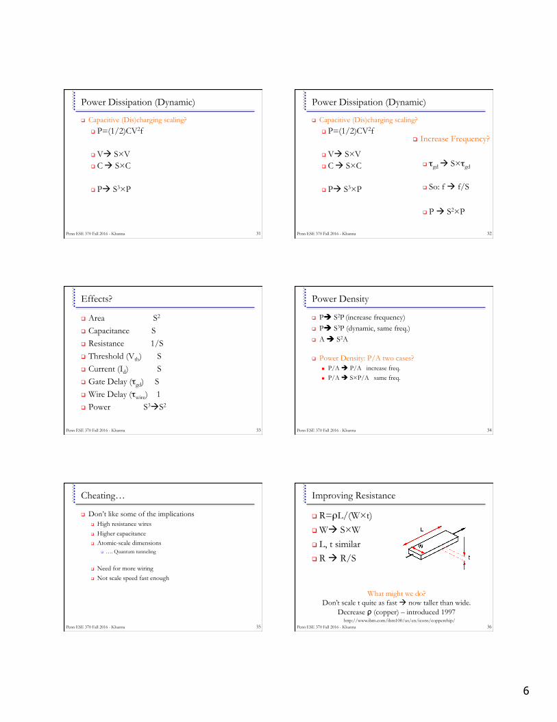
Improving Resistance
! R=ρL/(W×t) ! W$ S×W! L, t similar ! R $ R/S
What might we do? Don’t scale t quite as fast $ now taller than wide.
Decrease ρ (copper) – introduced 1997 http://www.ibm.com/ibm100/us/en/icons/copperchip/
Penn ESE 370 Fall 2016 - Khanna 36

7
Capacitance and Leakage
! Capacitance per unit area " Cox= εSiO2
/Tox
" Tox% S×Tox
" Cox % Cox/S
What’s wrong with tox = 1.2nm?
source: Borkar/Micro 2004
Penn ESE 370 Fall 2016 - Khanna 37
Capacitance and Leakage
! Capacitance per unit area " Cox= εSiO2
/Tox
" Tox% S×Tox
" Cox % Cox/S
What might we do? Reduce dielectric constant, ε, and increase
thickness to mimic tox scaling. Penn ESE 370 Fall 2016 - Khanna 38
ITRS 2009 Table PIDS3B Low Operating Power Technology Requirements
Grey cells delineate one of two time periods: either before initial production ramp has started for ultra-thin body fully depleted (UTB FD) SOI or multi-gate
(MG) MOSFETs, or beyond when planar bulk or UTB FD MOSFETs have reached the limits of practical scaling (see the text and the table notes for further
discussion).
Year of Production 2009 2010 2011 2012 2013 2014 2016 2016 2017 2018 2019 2020 2021 2022 2023 2024 MPU/ASIC Metal 1 (M1) ½ Pitch (nm) (contacted) 54 45 38 32 27 24 21 18.9 16.9 15 13.4 11.9 10.6 9.5 8.4 7.5 Lg: Physical Lgate for High Performance logic (nm) 29 27 24 22 20 18 17 15.3 14 12.8 11.7 10.7 9.7 8.9 8.1 7.4 Lg: Physical Lgate for Low OperatingPower (LOP) logic (nm) [1] 32 29 27 24 22 18 17 15.3 14 12.8 11.7 10.7 9.7 8.9 8.1 7.4 EOT: Equivalent Oxide Thickness (nm) [2] Extended planar bulk 1 0.9 0.9 0.85 0.8 UTB FD 0.9 0.85 0.8 0.75 0.7 MG 0.8 0.8 0.75 0.73 0.7 0.7 0.65 0.65 0.6 0.6 Gate poly depletion (nm) [3] Bulk 0.27 0.27 0 0 0 0 0 0 0 0 0 0 0 0 0 0 Channel doping (E18 /cm3) [4] Extended Planar Bulk 3 3.7 4.5 5 5.5 0.1 0.1 0.1 0.1 0.1 0.1 0.1 0.1 0.1 0.1 0.1 Junction depth or body Thickness (nm) [5] Extended Planar Bulk (junction) 14 13 11.5 10 9 UTB FD (body) 7 6.2 6 5.1 4.7 MG (body) 8 7.6 7 6.4 5.8 5.4 4.8 4.4 4.2 4 EOTelec: Electrical Equivalent Oxide Thickness (nm) [6] Extended Planar Bulk 1.64 1.53 1.23 1.18 1.14 UTB FD 1.3 1.25 1.2 1.15 1.1 MG 1.2 1.2 1.15 1.13 1.1 1.1 1.05 1.05 1 1
Penn ESE 370 Fall 2016 - Khanna 39
High-K dielectric Survey
Wong/IBM J. of R&D, V46N2/3P133—168, 2002 Penn ESE 370 Fall 2016 - Khanna 40
Intel NYT Announcement
! Intel Says Chips Will Run Faster, Using Less Power " NYT 1/27/07, John Markov " Claim: “most significant change in the
materials used to manufacture silicon chips since Intel pioneered the modern integrated-circuit transistor more than four decades ago”
" “Intel’s advance was in part in finding a new insulator composed of an alloy of hafnium…will replace the use of silicon dioxide.”
Penn ESE 370 Fall 2016 - Khanna 41
Wire Layers = More Wiring
Penn ESE 370 Fall 2016 - Khanna 42
8
Improving Gate Delay
# τgd=Q/I=(CV)/I # V$ S×V # Id=(µCOX/2)(W/L)(Vgs-VTH)2
# Id $ S×Id
# C $ S×C
# τgd $ S×τgd
# Lower C # Don’t scale V
Don’t scale V: V$V I$I/S
τgd $ S2×τgd
How might we accelerate?
Penn ESE 370 Fall 2016 - Khanna 43
But… Power Dissipation (Dynamic)
! Capacitive (Dis)charging
# P=(1/2)CV2f # V$ V# C $ S×C # P$ S×P
Penn ESE 370 Fall 2016 - Khanna 44
But… Power Dissipation (Dynamic)
! Capacitive (Dis)charging
# P=(1/2)CV2f # V$ V# C $ S×C # P$ S×P
! Increase Frequency? # f $ f/S2 ? # P $ P/S
If don’t scale V, power dissipation doesn’t’ scale down!
Penn ESE 370 Fall 2016 - Khanna 45
…And Power Density
! P$ P/S (increase frequency)! But… Α $ S2×Α! What happens to power density?
! P/A $ (1/S3)P
! Power Density Increases
…this is where some companies have gotten into trouble…
Penn ESE 370 Fall 2016 - Khanna 46
Historical Voltage Scaling
! Frequency impact? ! Power Density impact?
http://software.intel.com/en-us/articles/gigascale-integration-challenges-and-opportunities/
Penn ESE 370 Fall 2016 - Khanna 47
Scale V separately from S
! τgd=Q/I=(CV)/I ! V$U! Id=(µCOX/2)(W/L)(Vgs-VTH)2
! Id $ U2/S×Id
! C $ S×C
! τgd $ (SU/(U2/S))×τgd
! τgd $ (S2/U)×τgd
Ideal scale: S=1/100 V=1/100 τ=1/100 fideal=100
Cheating: S=1/100 V=1/10 τ=1/1000 fcheat=1000
fcheat/fideal=10
Penn ESE 370 Fall 2016 - Khanna 48
S=1/100 U=1/10

9
Power Density Impact
! P=1/2CV2 f ! P~= S U2 (U/S2) = U3/S ! P/A = (U3/S) / S2 = U3/S3
! U=1/10 S=1/100 ! P/A $ 1000 (P/A)
! P/A $ (1/S3)P (ideal scaling) ! P/A $ 1,000,000 (P/A) (ideal scaling)
Penn ESE 370 Fall 2016 - Khanna 49
uProc Clock Frequency
The Future of Computing Performance: Game Over or Next Level? National Academy Press, 2011
http://www.nap.edu/catalog.php?record_id=12980
MHz
Penn ESE 370 Fall 2016 - Khanna 50
uP Power Density
Watts
The Future of Computing Performance: Game Over or Next Level? National Academy Press, 2011
http://www.nap.edu/catalog.php?record_id=12980 Penn ESE 370 Fall 2016 - Khanna 51
Conventional Scaling
! Ends in your lifetime ! Perhaps already:
" "Basically, this is the end of scaling.” " May 2005, Bernard Meyerson, V.P. and chief technologist for
IBM's systems and technology group
Penn ESE 370 Fall 2016 - Khanna 52
ITRS 2.0 Report 2015
! “After 2021, the report forecasts, it will no longer be economically desirable for companies to continue traditional transistor miniaturization in microprocessors.”
Penn ESE 370 Fall 2016 - Khanna 53
Big Ideas
! Moderately predictable VLSI Scaling " unprecedented capacities/capability growth for
engineered systems " change
" be prepared to exploit " account for in comparing across time " …but not for much longer
Penn ESE 370 Fall 2016 - Khanna 54

10
Admin
! HW5 " More transistor practice " Hard – prepares you for design project 1 " Due Wednesday
! Midterm " Will finish grading and post grades this afternoon " Can come to my office to pick up otherwise will hand
back on Monday
Penn ESE 370 Fall 2016 - Khanna 55