universidade do algarve faculdade de ciências e...
TRANSCRIPT

http://w
3.ualg.pt/~jlongras/aulas/OC
S.html
José Figueiredo © 1999 S.O. Kasap 1
Universidade do AlgarveFaculdade de Ciências e Tecnologia
Departamento de FísicaAno lectivo 2015-2016
Unidade Curricular Sistemas de Comunicação ÓticaOptical Communication Systems
Mestrado Integrado em Engenharia Electrónica e TelecomunicaçõesMestrado em Engenharia Informática
José Figueiredo
http://w3.ualg.pt/~jlongras/aulas/OCS.html

http://w
3.ualg.pt/~jlongras/aulas/OC
S.html
José Figueiredo © 1999 S.O. Kasap 2
Ondas electromagnéticas
Electromagnetic waves
http://w
3.ualg.pt/~jlongras/aulas/OC
S.html
José Figueiredo © 1999 S.O. Kasap 3
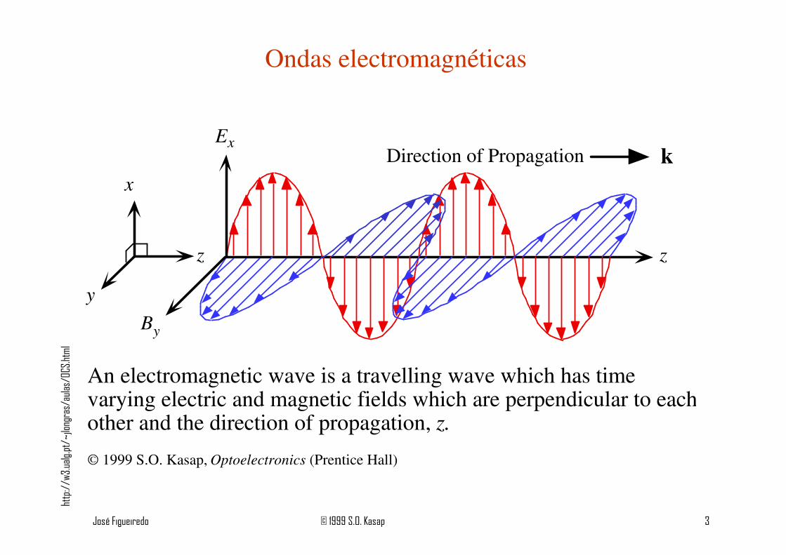
Ex
z
Direction of Propagation
By
z
x
y
k
An electromagnetic wave is a travelling wave which has timevarying electric and magnetic fields which are perpendicular to eachother and the direction of propagation, z.
© 1999 S.O. Kasap, Optoelectronics (Prentice Hall)
Ondas electromagnéticas

http://w
3.ualg.pt/~jlongras/aulas/OC
S.html
José Figueiredo © 1999 S.O. Kasap 4
z
Ex = E
osin(ωt–kz)
Ex
z
Propagation
E
B
k
E and B have constant phasein this xy plane; a wavefront
E
A plane EM wave travelling along z, has the same Ex (or By) at any point in agiven xy plane. All electric field vectors in a given xy plane are therefore in phase.The xy planes are of infinite extent in the x and y directions.
© 1999 S.O. Kasap, Optoelectronics (Prentice Hall)
Wave fronts– regions with the same phase

http://w
3.ualg.pt/~jlongras/aulas/OC
S.html
José Figueiredo © 1999 S.O. Kasap 5
y
z
k
Direction of propagation
r
O
θ
E(r,t)r′′′′
A travelling plane EM wave along a direction k.© 1999 S.O. Kasap, Optoelectronics (Prentice Hall)
Wave vector - Vector de onda

http://w
3.ualg.pt/~jlongras/aulas/OC
S.html
José Figueiredo © 1999 S.O. Kasap 6
k
Wave fronts
r
E
k
Wave fronts(constant phase surfaces)
z
λλλλλλλλ
λλλλ
Wave fronts
PO
P
A perfect spherical waveA perfect plane wave A divergent beam
(a) (b) (c)
Examples of possible EM waves
© 1999 S.O. Kasap, Optoelectronics (Prentice Hall)
Examples of electromagnetic wave fronts
http://w
3.ualg.pt/~jlongras/aulas/OC
S.html
José Figueiredo © 1999 S.O. Kasap 7
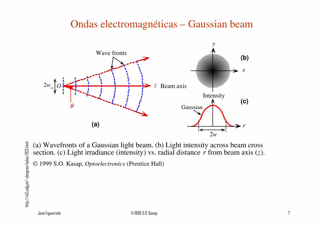
y
x
Wave fronts
z Beam axis
r
Intensity
(a)
(b)
(c)
2wo
θ
O
Gaussian
2w
(a) Wavefronts of a Gaussian light beam. (b) Light intensity across beam crosssection. (c) Light irradiance (intensity) vs. radial distance r from beam axis (z).
© 1999 S.O. Kasap, Optoelectronics (Prentice Hall)
Ondas electromagnéticas – Gaussian beam
http://w
3.ualg.pt/~jlongras/aulas/OC
S.html
José Figueiredo © 1999 S.O. Kasap 8
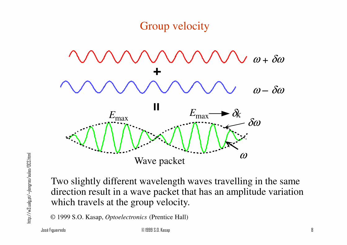
δω
ω
ω + δω
ω – δω
δkEmaxEmax
Wave packet
Two slightly different wavelength waves travelling in the samedirection result in a wave packet that has an amplitude variationwhich travels at the group velocity.
© 1999 S.O. Kasap, Optoelectronics (Prentice Hall)
Group velocity

http://w
3.ualg.pt/~jlongras/aulas/OC
S.html
José Figueiredo © 1999 S.O. Kasap 9
Refractive index n and the group index Ng of pureSiO2 (silica) glass as a function of wavelength.
Ng
n
500 700 900 1100 1300 1500 1700 1900
1.44
1.45
1.46
1.47
1.48
1.49
Wavelength (nm)
© 1999 S.O. Kasap, Optoelectronics (Prentice Hall)
Índice de refracção de grupo

http://w
3.ualg.pt/~jlongras/aulas/OC
S.html
José Figueiredo © 1999 S.O. Kasap 10
z
Propagation direction
E
B
k
Area A
v∆t
A plane EM wave travelling along k crosses an area A at right angles to thedirection of propagation. In time ∆t, the energy in the cylindrical volume Av∆t(shown dashed) flows through A .
© 1999 S.O. Kasap, Optoelectronics (Prentice Hall)
Vector de Poynting

http://w
3.ualg.pt/~jlongras/aulas/OC
S.html
José Figueiredo © 1999 S.O. Kasap 11
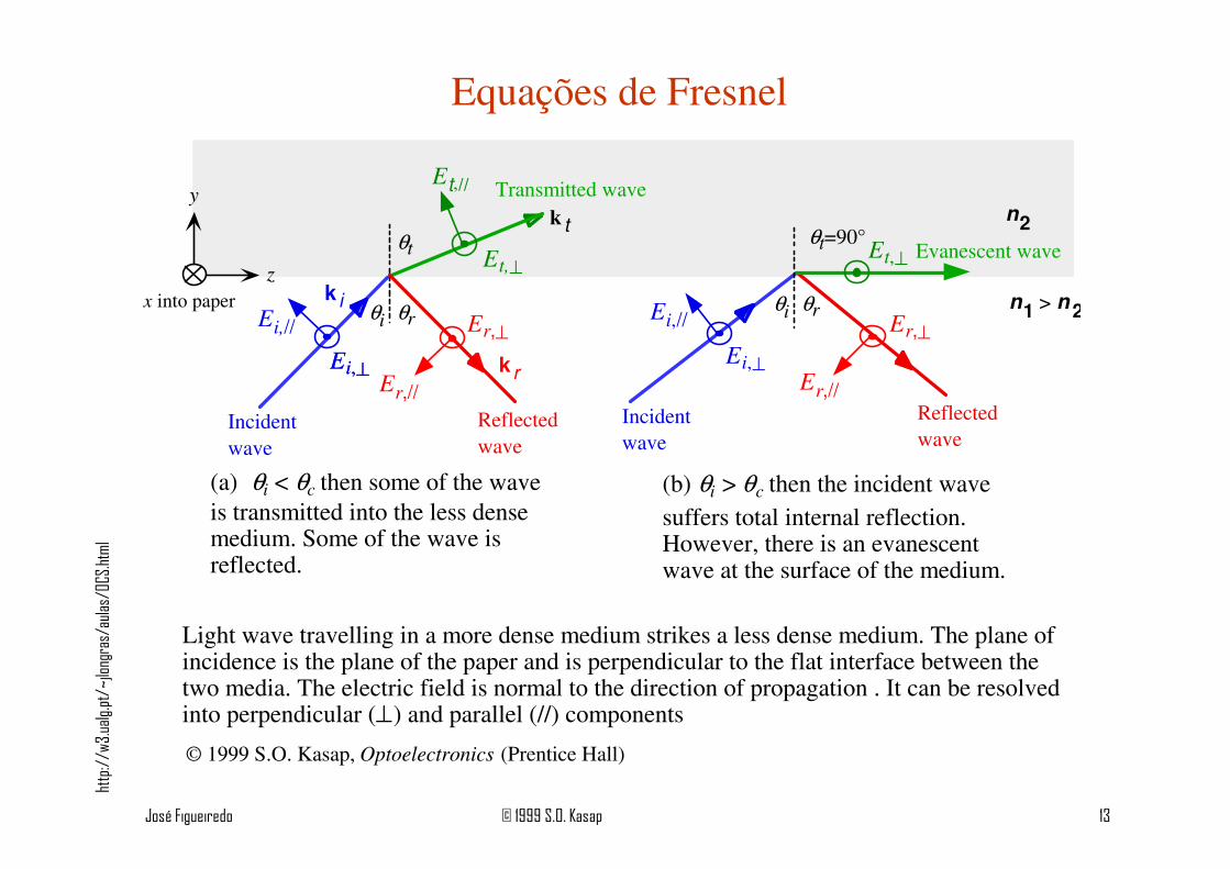
n2
z
y
O
θi
n1
Ai
λ λ
θrθi
Incident Light BiA
r
Br
θt θt
λt
Refracted Light
Reflected Light
kt
At
Bt
B′A
B
A′
A′′
θr
ki
kr
A light wave travelling in a medium with a greater refractive index ( n1 > n2) suffersreflection and refraction at the boundary.
© 1999 S.O. Kasap, Optoelectronics (Prentice Hall)
Reflexão e refracção

http://w
3.ualg.pt/~jlongras/aulas/OC
S.html
José Figueiredo © 1999 S.O. Kasap 12
n2
θi
n1 > n
2θ
i
Incidentlight
θt
Transmitted(refracted) light
Reflectedlight
kt
θi>θ
cθ
c
TIR
θc
Evanescent wave
ki
kr
(a) (b) (c)
Light wave travelling in a more dense medium strikes a less dense medium. Depending onthe incidence angle with respect to θc, which is determined by the ratio of the refractiveindices, the wave may be transmitted (refracted) or reflected. (a) θi < θc (b) θi = θc (c) θi
> θc and total internal reflection (TIR).
© 1999 S.O. Kasap, Optoelectronics (Prentice Hall)
Leis de Snell
http://w
3.ualg.pt/~jlongras/aulas/OC
S.html
José Figueiredo © 1999 S.O. Kasap 13
k i
n2
n1 > n 2
θt=90°Evanescent wave
Reflectedwave
Incidentwave
θi θr
Er,//
Er,⊥
Ei,⊥
Ei,//
Et,⊥
(b) θi > θc then the incident wavesuffers total internal reflection.However, there is an evanescentwave at the surface of the medium.
z
y
x into paperθi θr
Incidentwave
θt
Transmitted wave
Ei,//
Ei,⊥Er,//
Et,//
Et,⊥
Er,⊥
Reflectedwave
k t
k r
Light wave travelling in a more dense medium strikes a less dense medium. The plane ofincidence is the plane of the paper and is perpendicular to the flat interface between thetwo media. The electric field is normal to the direction of propagation . It can be resolvedinto perpendicular (⊥) and parallel (//) components
(a) θi < θc then some of the waveis transmitted into the less densemedium. Some of the wave isreflected.
Ei,⊥
© 1999 S.O. Kasap, Optoelectronics (Prentice Hall)
Equações de Fresnel
http://w
3.ualg.pt/~jlongras/aulas/OC
S.html
José Figueiredo © 1999 S.O. Kasap 14
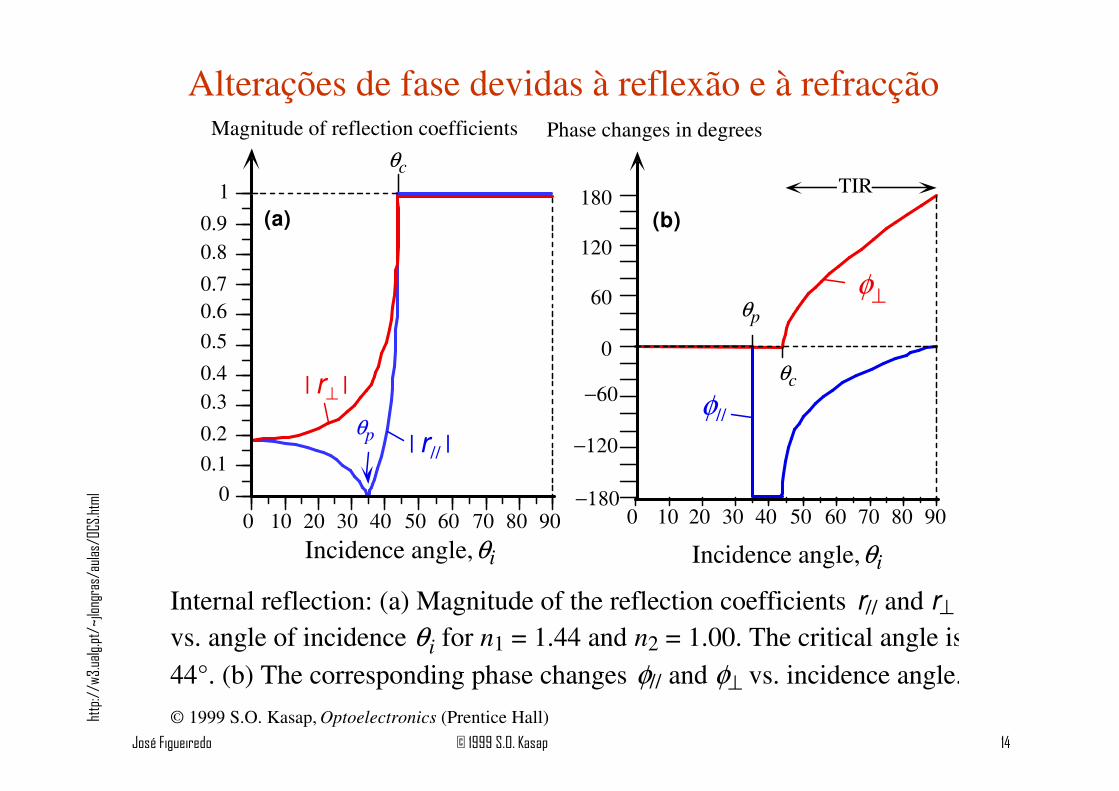
Internal reflection: (a) Magnitude of the reflection coefficients r// and r⊥
vs. angle of incidence θi for n1 = 1.44 and n2 = 1.00. The critical angle is44°. (b) The corresponding phase changes φ// and φ⊥ vs. incidence angle.
φ//
φ⊥
(b)
60
120
180
Incidence angle, θi
0
0.1
0.2
0.30.4
0.5
0.60.7
0.80.9
1
0 10 20 30 40 50 60 70 80 90
| r// |
| r⊥ |
θc
θp
Incidence angle, θi
(a)
Magnitude of reflection coefficients Phase changes in degrees
0 10 20 30 40 50 60 70 80 90
θc
θp
TIR
0
−60
−120
−180
© 1999 S.O. Kasap, Optoelectronics (Prentice Hall)
Alterações de fase devidas à reflexão e à refracção

http://w
3.ualg.pt/~jlongras/aulas/OC
S.html
José Figueiredo © 1999 S.O. Kasap 15
The reflection coefficients r// and r⊥ vs. angleof incidence θi for n1 = 1.00 and n2 = 1.44.
-1-0.8
-0.6
-0.4
-0.2
0
0.2
0.4
0.6
0.81
0 10 20 30 40 50 60 70 80 90
θp r//
r⊥
Incidence angle, θi
External reflection
© 1999 S.O. Kasap, Optoelectronics (Prentice Hall)
Coeficientes de reflexão

http://w
3.ualg.pt/~jlongras/aulas/OC
S.html
José Figueiredo © 1999 S.O. Kasap 16
θi
n2
n1 > n
2
Incidentlight
Reflectedlight
θr
∆z
Virtual reflecting plane
Penetration depth, δz
y
The reflected light beam in total internal reflection appears to have been laterally shifted byan amount ∆z at the interface.
A
B
© 1999 S.O. Kasap, Optoelectronics (Prentice Hall)
Profundidade de penetração

http://w
3.ualg.pt/~jlongras/aulas/OC
S.html
José Figueiredo © 1999 S.O. Kasap 17
θi
n2
n1 > n
2
Incidentlight
Reflectedlight
θr
When medium B is thin (thickness d is small), the field penetrates tothe BC interface and gives rise to an attenuated wave in medium C.The effect is the tunnelling of the incident beam in A through B to C.
z
y
d
n1
AB
C
© 1999 S.O. Kasap, Optoelectronics (Prentice Hall)
Efeito de túnel óptico

http://w
3.ualg.pt/~jlongras/aulas/OC
S.html
José Figueiredo © 1999 S.O. Kasap 18
Incidentlight
Reflectedlight
θi > θc
TIR
(a)
Glass prism
θi > θc
FTIR
(b)
n1
n1n
2 n1
B = Low refractive indextransparent film ( n
2)
ACA
Reflected
Transmitted
(a) A light incident at the long face of a glass prism suffers TIR; the prism deflects thelight.(b) Two prisms separated by a thin low refractive index film forming a beam-splitter cube.The incident beam is split into two beams by FTIR.
Incidentlight
© 1999 S.O. Kasap, Optoelectronics (Prentice Hall)
Reflexão interna total frustrada

http://w
3.ualg.pt/~jlongras/aulas/OC
S.html
José Figueiredo © 1999 S.O. Kasap 19
TimeP
Q
Field
υ
Amplitude
υο
∞−∞
Time
(a)
υ
Amplitude
υο
∆υ = 1/∆t
Time
(b)
P Q
l = c∆t
Space
∆t
(c)
υ
Amplitude
(a) A sine wave is perfectly coherent and contains a well-defined frequency υo. (b) A finitewave train lasts for a duration ∆t and has a length l. Its frequency spectrum extends over∆υ = 1/∆t. It has a coherence time ∆t and a coherence length l. (c) White light exhibitspractically no coherence.
© 1999 S.O. Kasap, Optoelectronics (Prentice Hall)
Coerência temporal e espacial

http://w
3.ualg.pt/~jlongras/aulas/OC
S.html
José Figueiredo © 1999 S.O. Kasap 20
c
(a)
Time
(b)
A
B
∆t
Interference No interferenceNo interference
Space
c
P
Q
Source
Spatially coherent source
An incoherent beam(c)
(a) Two waves can only interfere over the time interval ∆t. (b) Spatial coherence involvescomparing the coherence of waves emitted from different locations on the source. (c) Anincoherent beam.
© 1999 S.O. Kasap, Optoelectronics (Prentice Hall)
Coerência temporal e espacial e o fenómeno de interferência

http://w
3.ualg.pt/~jlongras/aulas/OC
S.html
José Figueiredo © 1999 S.O. Kasap 21
Light intensity pattern
Incident light wave
Diffracted beam
Circular aperture
A light beam incident on a small circular aperture becomes diffracted and its lightintensity pattern after passing through the aperture is a diffraction pattern with circularbright rings (called Airy rings). If the screen is far away from the aperture, this would be aFraunhofer diffraction pattern.
© 1999 S.O. Kasap, Optoelectronics (Prentice Hall)
Difracção

http://w
3.ualg.pt/~jlongras/aulas/OC
S.html
José Figueiredo © 1999 S.O. Kasap 22
Incident plane wave
Newwavefront
A secondarywave source
(a) (b)
Another newwavefront (diffracted)
zθθθθ
(a) Huygens-Fresnel principles states that each point in the aperture becomes a source ofsecondary waves (spherical waves). The spherical wavefronts are separated by λ. The newwavefront is the envelope of the all these spherical wavefronts. (b) Another possiblewavefront occurs at an angle θ to the z-direction which is a diffracted wave.
© 1999 S.O. Kasap, Optoelectronics (Prentice Hall)
Princípio de Huygens-Fresnel

http://w
3.ualg.pt/~jlongras/aulas/OC
S.html
José Figueiredo © 1999 S.O. Kasap 23
θ
A
ysinθ
y
Y
θ
θ = 0
δy
zδy
ScreenIncidentlight wave
θ
R = Large
θ
c
b
Light intensity
a
y
y
z
(a) (b)
(a) The aperture is divided into N number of point sources each occupying δy withamplitude ∝ δy. (b) The intensity distribution in the received light at the screen far awayfrom the aperture: the diffraction pattern
Incidentlight wave
© 1999 S.O. Kasap, Optoelectronics (Prentice Hall)
Difracção de uma fenda “infinita”

http://w
3.ualg.pt/~jlongras/aulas/OC
S.html
José Figueiredo © 1999 S.O. Kasap 24
The rectangular aperture of dimensions a × b on the leftgives the diffraction pattern on the right.
a
b
© 1999 S.O. Kasap, Optoelectronics (Prentice Hall)
Difracção de uma abertura rectangular

http://w
3.ualg.pt/~jlongras/aulas/OC
S.html
José Figueiredo © 1999 S.O. Kasap 25
∆θ
S1
S2
S1
S2
A1
A2
I
y
Screen
∆θs
L
Resolution of imaging systems is limited by diffraction effects. As points S1 and S2
get closer, eventually the Airy disks overlap so much that the resolution is lost.
© 1999 S.O. Kasap, Optoelectronics (Prentice Hall)
Poder resolvente de um sistema de imagem

http://w
3.ualg.pt/~jlongras/aulas/OC
S.html
José Figueiredo © 1999 S.O. Kasap 26
d
z
y
Incidentlight wave
Diffraction grating
One possiblediffracted beam
θ
a
Intensity
y
m = 0
m = 1
m = -1
m = 2
m = -2
Zero-order
First-order
First-order
Second-order
Second-order
Single slitdiffractionenvelope
dsinθ
(a) (b)
(a) A diffraction grating with N slits in an opaque scree. (b) The diffracted lightpattern. There are distinct beams in certain directions (schematic)
© 1999 S.O. Kasap, Optoelectronics (Prentice Hall)
Redes de difracção

http://w
3.ualg.pt/~jlongras/aulas/OC
S.html
José Figueiredo © 1999 S.O. Kasap 27
Incidentlight wave
m = 0
m = -1
m = 1
Zero-order
First-order
First-order
(a) Transmission grating (b) Reflection grating
Incidentlight wave
Zero-orderFirst-order
First-order
(a) Ruled periodic parallel scratches on a glass serve as a transmission grating. (b) Areflection grating. An incident light beam results in various "diffracted" beams. Thezero-order diffracted beam is the normal reflected beam with an angle of reflection equalto the angle of incidence.
© 1999 S.O. Kasap, Optoelectronics (Prentice Hall)
Redes de difracção de transmissão e de reflexão
http://w
3.ualg.pt/~jlongras/aulas/OC
S.html
José Figueiredo © 1999 S.O. Kasap 28
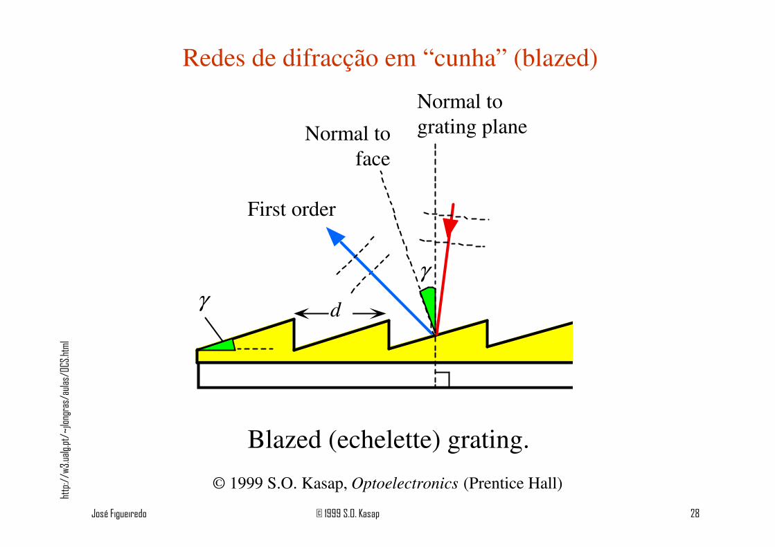
First order
γ
Normal tograting planeNormal to
face
d
γ
Blazed (echelette) grating.
© 1999 S.O. Kasap, Optoelectronics (Prentice Hall)
Redes de difracção em “cunha” (blazed)

http://w
3.ualg.pt/~jlongras/aulas/OC
S.html
José Figueiredo © 1999 S.O. Kasap 29
Two confocal spherical mirrors reflect waves to and fromeach other. F is the focal point and R is the radius. Theoptical cavity contains a Gaussian beam
Wave front
Spherical mirrorOptical cavity
Spherical mirror
A B
L
R
© 1999 S.O. Kasap, Optoelectronics (Prentice Hall)
2θ
R
F
Exemplo de uma cavidade óptica ressonante

http://w
3.ualg.pt/~jlongras/aulas/OC
S.html
José Figueiredo © 1999 S.O. Kasap 30
n1
n2
n3
B1
A1 A2 A3A0
C1
B2
B3
B4
B5
C2 C3
B6
Thin film coating of refractive index n2on a semiconductor device
© 1999 S.O. Kasap, Optoelectronics (Prentice Hall)
Filme fino – camada anti-reflectora
http://w
3.ualg.pt/~jlongras/aulas/OC
S.html
José Figueiredo © 1999 S.O. Kasap 31
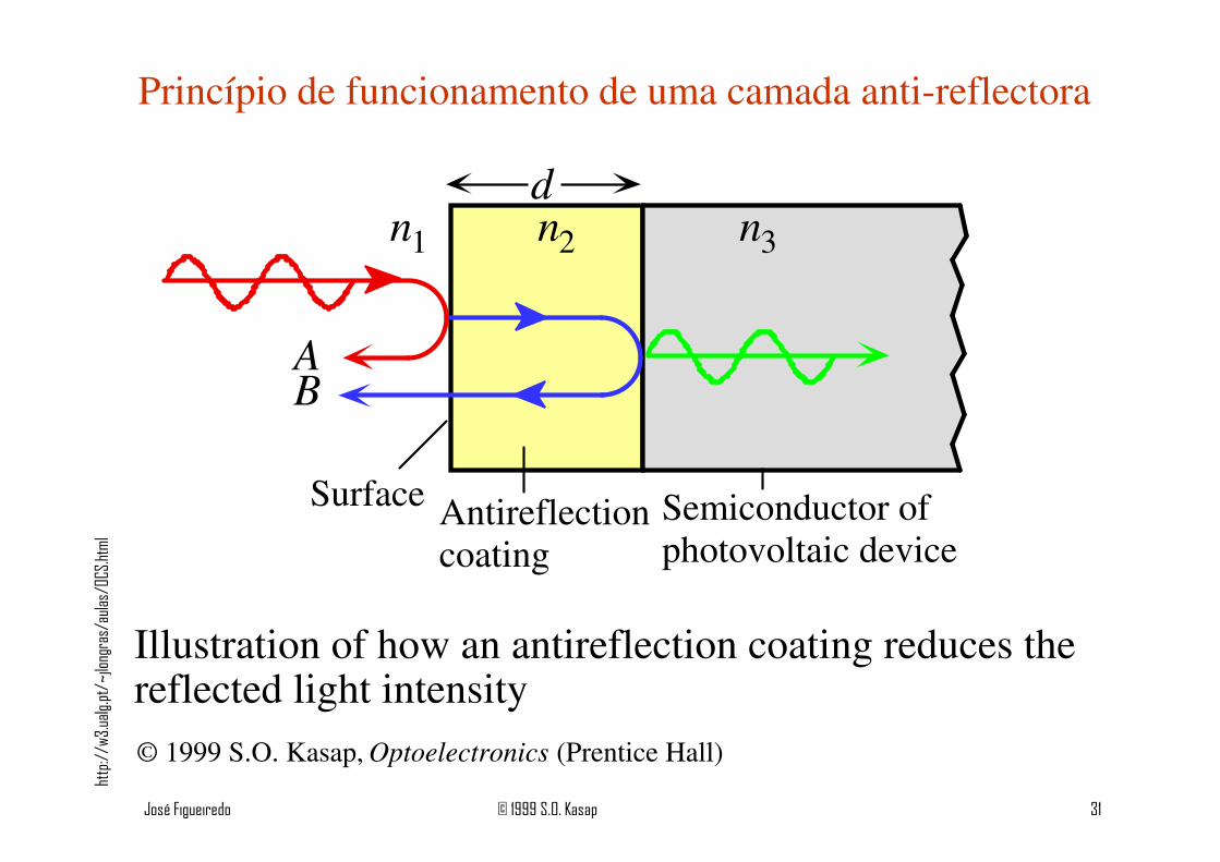
d
Semiconductor ofphotovoltaic device
Antireflectioncoating
Surface
Illustration of how an antireflection coating reduces thereflected light intensity
n1 n2 n3
AB
© 1999 S.O. Kasap, Optoelectronics (Prentice Hall)
Princípio de funcionamento de uma camada anti-reflectora

http://w
3.ualg.pt/~jlongras/aulas/OC
S.html
José Figueiredo © 1999 S.O. Kasap 32
n1 n2
AB
n1 n2
C
Schematic illustration of the principle of the dielectric mirror with many low and highrefractive index layers and its reflectance.
Reflectance
λ (nm)0
1
330 550 770
1 2 21
λo
λ1/4 λ2/4
© 1999 S.O. Kasap, Optoelectronics (Prentice Hall)
Espelho dieléctrico

http://w
3.ualg.pt/~jlongras/aulas/OC
S.html
José Figueiredo © 1999 S.O. Kasap 33
A
B
L
M1 M2 m = 1
m = 2
m = 8
Relative intensity
υ
δυm
υm υm + 1υm - 1
(a) (b) (c)
R ~ 0.4
R ~ 0.81 υf
Schematic illustration of the Fabry-Perot optical cavity and its properties. (a) Reflectedwaves interfere. (b) Only standing EM waves, modes, of certain wavelengths are allowedin the cavity. (c) Intensity vs. frequency for various modes. R is mirror reflectance andlower R means higher loss from the cavity.
© 1999 S.O. Kasap, Optoelectronics (Prentice Hall)
Cavidade óptica Fabry-Perot
http://w
3.ualg.pt/~jlongras/aulas/OC
S.html
José Figueiredo © 1999 S.O. Kasap 34
L λλ
mλ
m - 1
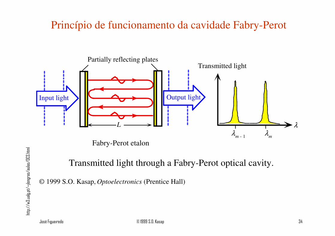
Fabry-Perot etalon
Partially reflecting plates
Output lightInput light
Transmitted light
Transmitted light through a Fabry-Perot optical cavity.
© 1999 S.O. Kasap, Optoelectronics (Prentice Hall)
Princípio de funcionamento da cavidade Fabry-Perot

http://w
3.ualg.pt/~jlongras/aulas/OC
S.html
José Figueiredo © 1999 S.O. Kasap 35
L
Fabry-Perot etalon
Output light
Input light
θ
θ
θ
θ
LensBroadmonochromaticsource Screen
Screen
k
FP etalon
Fabry-Perot optical resonator and the Fabry-Perot interferometer (schematic)
© 1999 S.O. Kasap, Optoelectronics (Prentice Hall)
Interferómetro Fabry-Perot
José Figueiredo © 1999 S.O. Kasap 36
Guias de Onda e Fibras Ópticas

http://w
3.ualg.pt/~jlongras/aulas/OC
S.html
José Figueiredo © 1999 S.O. Kasap 37
n1
n3
n2Air
Glass substrate
Thin layer
(a)
Glass substrate
Thin layer
PrismLaser light
d = Adjustable coupling gap
(b)
(a) Light propagation along an optical guide. (b) Coupling of laser light into a thin layer -optical guide - using a prism. The light propagates along the thin layer.
© 1999 S.O. Kasap, Optoelectronics (Prentice Hall)
Princípio do guia de onda e acoplamento de luz

http://w
3.ualg.pt/~jlongras/aulas/OC
S.html
José Figueiredo © 1999 S.O. Kasap 38
Light
n2
A planar dielectric waveguide has a central rectangular region ofhigher refractive index n1 than the surrounding region which hasa refractive index n2. It is assumed that the waveguide isinfinitely wide and the central region is of thickness 2a. It isilluminated at one end by a monochromatic light source.
n2
n1 > n2
Light
Light Light
© 1999 S.O. Kasap, Optoelectronics (Prentice Hall)
Guia de onda planar
http://w
3.ualg.pt/~jlongras/aulas/OC
S.html
José Figueiredo © 1999 S.O. Kasap 39
n2
n2
d = 2a
θθk1
Light
A
B
C
λ
β
κ
E
θn
1
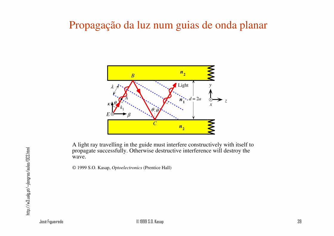
A light ray travelling in the guide must interfere constructively with itself topropagate successfully. Otherwise destructive interference will destroy thewave.
© 1999 S.O. Kasap, Optoelectronics (Prentice Hall)
z
y
x
Propagação da luz num guias de onda planar

http://w
3.ualg.pt/~jlongras/aulas/OC
S.html
José Figueiredo © 1999 S.O. Kasap 40
n2
n2
z2a
y
A
1
2 1
B
θθ
θA′
B′
Cπ−2θ 2θ−π/2
k1
Ex
n1
Two arbitrary waves 1 and 2 that are initially in phase must remain in phaseafter reflections. Otherwise the two will interfere destructively and cancel eachother.
© 1999 S.O. Kasap, Optoelectronics (Prentice Hall)
Propagação da luz num guias de onda planar

http://w
3.ualg.pt/~jlongras/aulas/OC
S.html
José Figueiredo © 1999 S.O. Kasap 41
n2
z
ay
A
1
2
θθ
A′
C
kE
x
y
a−y
Guide center
π−2θ
Interference of waves such as 1 and 2 leads to a standing wave pattern along the y-direction which propagates along z.
© 1999 S.O. Kasap, Optoelectronics (Prentice Hall)
Propagação da luz num guias de onda planar
http://w
3.ualg.pt/~jlongras/aulas/OC
S.html
José Figueiredo © 1999 S.O. Kasap 42
n2
Light
n2
n1
y
E(y)
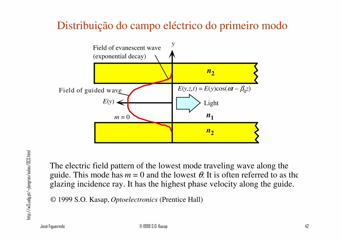
E(y,z,t) = E(y)cos(ωt – β0z)
m = 0
Field of evanescent wave(exponential decay)
Field of guided wave
The electric field pattern of the lowest mode traveling wave along theguide. This mode has m = 0 and the lowest θ. It is often referred to as theglazing incidence ray. It has the highest phase velocity along the guide.
© 1999 S.O. Kasap, Optoelectronics (Prentice Hall)
Distribuição do campo eléctrico do primeiro modo

http://w
3.ualg.pt/~jlongras/aulas/OC
S.html
José Figueiredo © 1999 S.O. Kasap 43
y
E(y)m = 0 m = 1 m = 2
Cladding
Cladding
Core 2an1
n2
n2
The electric field patterns of the first three modes (m = 0, 1, 2)traveling wave along the guide. Notice different extents of fieldpenetration into the cladding.
© 1999 S.O. Kasap, Optoelectronics (Prentice Hall)
Distribuição do campo eléctrico dos 3 1ºs modos
http://w
3.ualg.pt/~jlongras/aulas/OC
S.html
José Figueiredo © 1999 S.O. Kasap 44
Low order modeHigh order mode
Cladding
Core
Light pulse
t0 t
Spread, ∆τ
Broadenedlight pulse
IntensityIntensity
Axial
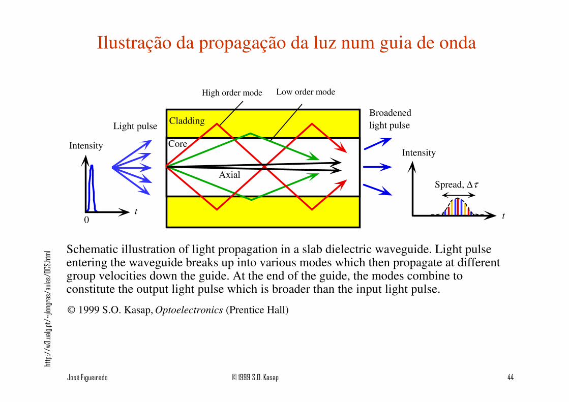
Schematic illustration of light propagation in a slab dielectric waveguide. Light pulseentering the waveguide breaks up into various modes which then propagate at differentgroup velocities down the guide. At the end of the guide, the modes combine toconstitute the output light pulse which is broader than the input light pulse.
© 1999 S.O. Kasap, Optoelectronics (Prentice Hall)
Ilustração da propagação da luz num guia de onda
http://w
3.ualg.pt/~jlongras/aulas/OC
S.html
José Figueiredo © 1999 S.O. Kasap 45
θθ
E⊥
By
Bz
z
y
O
θθ
B⊥
E// Ey
Ez
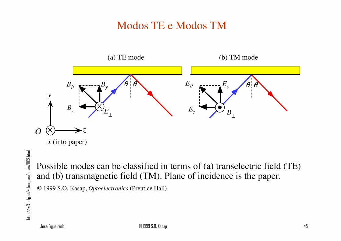
(b) TM mode(a) TE mode
B//
x (into paper)
Possible modes can be classified in terms of (a) transelectric field (TE)and (b) transmagnetic field (TM). Plane of incidence is the paper.© 1999 S.O. Kasap, Optoelectronics (Prentice Hall)
Modos TE e Modos TM
http://w
3.ualg.pt/~jlongras/aulas/OC
S.html
José Figueiredo © 1999 S.O. Kasap 46
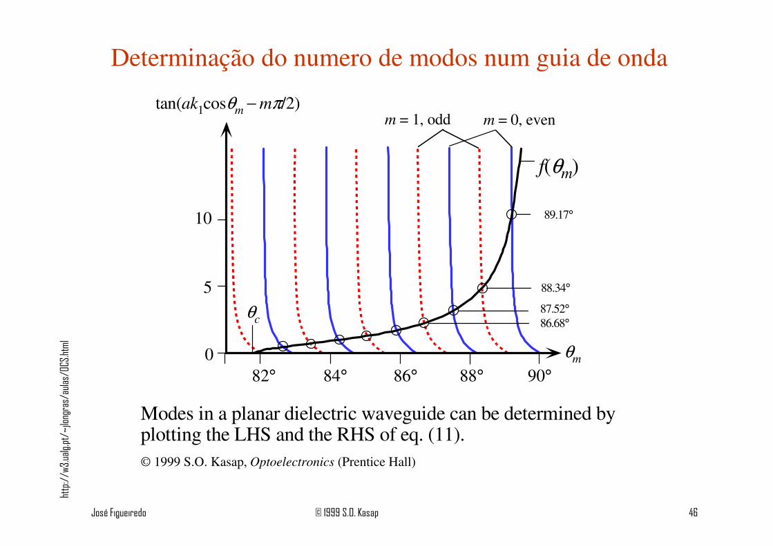
10
5
082° 84° 86° 88° 90°
θm
f(θm)
m = 0, evenm = 1, odd
89.17°
88.34°
87.52°86.68°
θc
tan(ak1cosθm − mπ/2)
Modes in a planar dielectric waveguide can be determined byplotting the LHS and the RHS of eq. (11).© 1999 S.O. Kasap, Optoelectronics (Prentice Hall)
Determinação do numero de modos num guia de onda

http://w
3.ualg.pt/~jlongras/aulas/OC
S.html
José Figueiredo © 1999 S.O. Kasap 47
βm
ωSlope = c/n2
Slope = c/n1
TE0
ωcut-off
TE1
TE2
Schematic dispersion diagram, ω vs. β for the slab waveguide for various TEm. modes.ωcut–off corresponds to V = π/2. The group velocity vg at any ω is the slope of the ω vs. βcurve at that frequency.
© 1999 S.O. Kasap, Optoelectronics (Prentice Hall)
Dispersão modal
http://w
3.ualg.pt/~jlongras/aulas/OC
S.html
José Figueiredo © 1999 S.O. Kasap 48
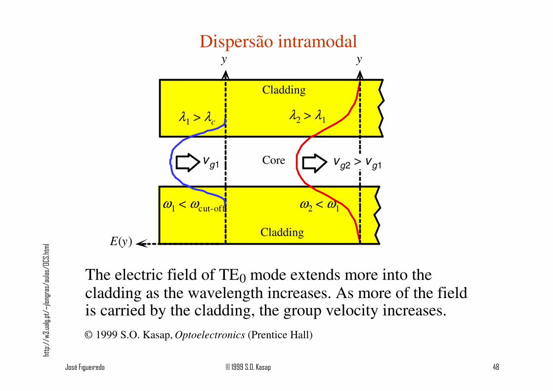
y
E(y)
Cladding
Cladding
Core
λ2 > λ1λ1 > λc
ω2 < ω1ω1 < ωcut-off
vg1
y
vg2 > vg1
The electric field of TE0 mode extends more into thecladding as the wavelength increases. As more of the fieldis carried by the cladding, the group velocity increases.
© 1999 S.O. Kasap, Optoelectronics (Prentice Hall)
Dispersão intramodal

http://w
3.ualg.pt/~jlongras/aulas/OC
S.html
José Figueiredo © 1999 S.O. Kasap 49
y
n2 n1
Cladding
Core z
y
r
φφφφ
Fiber axis
The step index optical fiber. The central region, the core, has greater refractiveindex than the outer region, the cladding. The fiber has cylindrical symmetry. Weuse the coordinates r, φ, z to represent any point in the fiber. Cladding isnormally much thicker than shown.
© 1999 S.O. Kasap, Optoelectronics (Prentice Hall)
n
Fibra óptica com perfil de índice em degrau

http://w
3.ualg.pt/~jlongras/aulas/OC
S.html
José Figueiredo © 1999 S.O. Kasap 50
Fiber axis
12
34
5
Skew ray1
3
2
4
5
Fiber axis
1
2
3Meridional ray
1, 3
2
(a) A meridionaray alwayscrosses the fibeaxis.
(b) A skew raydoes not haveto cross thefiber axis. Itzigzags aroundthe fiber axis.
Illustration of the difference between a meridional ray and a skew ray.Numbers represent reflections of the ray.
Along the fiber
Ray path projectedon to a plane normalto fiber axis
Ray path along the fiber
© 1999 S.O. Kasap, Optoelectronics (Prentice Hall)
Raios meridionais e raios “skew”

http://w
3.ualg.pt/~jlongras/aulas/OC
S.html
José Figueiredo © 1999 S.O. Kasap 51
E
r
E01
Core
Cladding
The electric field distribution of the fundamental modein the transverse plane to the fiber axis z. The lightintensity is greatest at the center of the fiber. Intensitypatterns in LP01, LP11 and LP21 modes.
(a) The electric fieldof the fundamentalmode
(b) The intensity inthe fundamentalmode LP01
(c) The intensityin LP11
(d) The intensityin LP21
© 1999 S.O. Kasap, Optoelectronics (Prentice Hall)
Distribuição do campo eléctrico e intensidade luminosa

http://w
3.ualg.pt/~jlongras/aulas/OC
S.html
José Figueiredo © 1999 S.O. Kasap 52
0 2 4 61 3 5V
b
1
0
0.8
0.6
0.4
0.2
LP01
LP11
LP21
LP02
2.405
Normalized propagation constant b vs. V-numberfor a step index fiber for various LP modes.© 1999 S.O. Kasap, Optoelectronics (Prentice Hall)
Constante de propagação normaliza vs número V

http://w
3.ualg.pt/~jlongras/aulas/OC
S.html
José Figueiredo © 1999 S.O. Kasap 53
Cladding
Coreα < αm a x
A
B
θ < θc
A
B
θ > θc
α > αm a x
n0 n1
n2
Lost
Propagates
Maximum acceptance angleαmax is that which just givestotal internal reflection at thecore-cladding interface, i.e.when α = αmax then θ = θc.Rays with α > αmax (e.g. rayB) become refracted andpenetrate the cladding and areeventually lost.
Fiber axis
© 1999 S.O. Kasap, Optoelectronics (Prentice Hall)
Ângulo de aceitação máxima

http://w
3.ualg.pt/~jlongras/aulas/OC
S.html
José Figueiredo © 1999 S.O. Kasap 54
τt
Spread, ² τ
t0
λ
Spectrum, ² λ
λ1λ2λo
Intensity Intensity Intensity
Cladding
CoreEmitter
Very shortlight pulse
vg(λ2)
vg(λ1)
Input
Output
All excitation sources are inherently non-monochromatic and emit within aspectrum, ² λ, of wavelengths. Waves in the guide with different free spacewavelengths travel at different group velocities due to the wavelength dependenceof n1. The waves arrive at the end of the fiber at different times and hence result ina broadened output pulse.
© 1999 S.O. Kasap, Optoelectronics (Prentice Hall)
Dispersão em fibras mono-modo

http://w
3.ualg.pt/~jlongras/aulas/OC
S.html
José Figueiredo © 1999 S.O. Kasap 55
0
1.2 1.3 1.4 1.5 1.61.1-30
20
30
10
-20
-10
λ (µm)
Dm
Dm + Dw
Dwλ0
Dispersion coefficient (ps km -1 nm-1)
Material dispersion coefficient (Dm) for the core material (taken asSiO2), waveguide dispersion coefficient (Dw) (a = 4.2 µm) and thetotal or chromatic dispersion coefficient Dch (= Dm + Dw) as afunction of free space wavelength, λ.
© 1999 S.O. Kasap, Optoelectronics (Prentice Hall)
Dispersão material e dispersão do guia de onda

http://w
3.ualg.pt/~jlongras/aulas/OC
S.html
José Figueiredo © 1999 S.O. Kasap 56
Dispersão devida à polarização
Core
z
n1 x
// x
n1 y
// y
Ey
Ex
Ex
Ey
E
∆τ = Pulse spread
Input light pulse
Output light pulset
t
∆τ
Intensity
Suppose that the core refractive index has different values along two orthogonaldirections corresponding to electric field oscillation direction (polarizations). We cantake x and y axes along these directions. An input light will travel along the fiber with Ex
and Ey polarizations having different group velocities and hence arrive at the output atdifferent times
© 1999 S.O. Kasap, Optoelectronics (Prentice Hall)

http://w
3.ualg.pt/~jlongras/aulas/OC
S.html
José Figueiredo © 1999 S.O. Kasap 57
20
-10
-20
-30
10
1.1 1.2 1.3 1.4 1.5 1.6 1.7
0
30
λ (µm)
Dm
Dw
Dch = D m + Dw
λ1
Dispersion coefficient (ps km -1 nm-1)
λ2
n
r
Thin layer of claddingwith a depressed index
Dispersion flattened fiber example. The material dispersion coefficient (Dm) for thecore material and waveguide dispersion coefficient (Dw) for the doubly clad fiberresult in a flattened small chromatic dispersion between λ1 and λ2.
© 1999 S.O. Kasap, Optoelectronics (Prentice Hall)
Dispersão em fibras “flattened”

http://w
3.ualg.pt/~jlongras/aulas/OC
S.html
José Figueiredo © 1999 S.O. Kasap 58
Material and waveguide dispersion coefficients in anoptical fiber with a core SiO2-13.5%GeO2 for a = 2.5to 4 µm.
0
–10
10
20
1.2 1.3 1.4 1.5 1.6–20
λ (µm)
Dm
Dw
SiO2-13.5%GeO2
2.5
3.03.54.0a (µm)
Dispersion coefficient (ps km-1 nm-1)
© 1999 S.O. Kasap, Optoelectronics (Prentice Hall)
Dispersão em fibras ópticas de vidro

http://w
3.ualg.pt/~jlongras/aulas/OC
S.html
José Figueiredo © 1999 S.O. Kasap 59
t0
Emitter
Very shortlight pulses
Input Output
Fiber
PhotodetectorDigital signal
Information Information
t0
~2² τ1/2
T
t
Output IntensityInput Intensity
² τ1/2
An optical fiber link for transmitting digital information and the effect ofdispersion in the fiber on the output pulses.
© 1999 S.O. Kasap, Optoelectronics (Prentice Hall)
“Bit rate” e Dispersão

http://w
3.ualg.pt/~jlongras/aulas/OC
S.html
José Figueiredo © 1999 S.O. Kasap 60
t
Output optical power
∆τ1/2
T = 4σ1
0.50.61 2σ
A Gaussian output light pulse and some tolerable intersymbolinterference between two consecutive output light pulses (y-axis inrelative units). At time t = σ from the pulse center, the relativemagnitude is e-1/2 = 0.607 and full width root mean square (rms)spread is ∆τrms = 2σ.
© 1999 S.O. Kasap, Optoelectronics (Prentice Hall)
Interferência intersimbólica tolerável
http://w
3.ualg.pt/~jlongras/aulas/OC
S.html
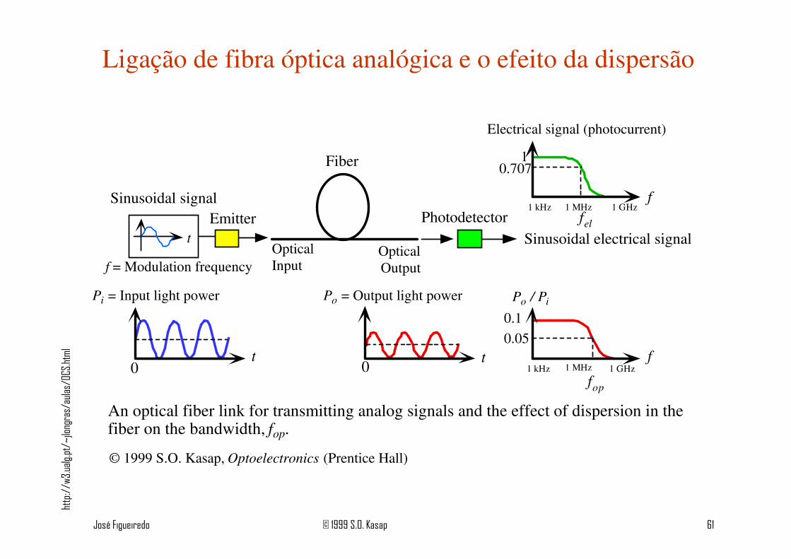
José Figueiredo © 1999 S.O. Kasap 61
t0
Pi = Input light power
Emitter
OpticalInput
OpticalOutput
Fiber
PhotodetectorSinusoidal signal
Sinusoidal electrical signalt
t0
f1 kHz 1 MHz 1 GHz
Po / Pi
fop
0.1
0.05
f = Modulation frequency
An optical fiber link for transmitting analog signals and the effect of dispersion in thefiber on the bandwidth, fop.
Po = Output light power
Electrical signal (photocurrent)
fel
10.707
f1 kHz 1 MHz 1 GHz
© 1999 S.O. Kasap, Optoelectronics (Prentice Hall)
Ligação de fibra óptica analógica e o efeito da dispersão

http://w
3.ualg.pt/~jlongras/aulas/OC
S.html
José Figueiredo © 1999 S.O. Kasap 62
n1
n2
21
3
nO
n1
21
3
n
n2
OO' O''
n2
(a) Multimode stepindex fiber. Ray pathsare different so thatrays arrive at differenttimes.
(b) Graded index fiber.Ray paths are differentbut so are the velocitiesalong the paths so thatall the rays arrive at thesame time.
23
© 1999 S.O. Kasap, Optoelectronics (Prentice Hall)
Fibras ópticas com índice gradual
http://w
3.ualg.pt/~jlongras/aulas/OC
S.html
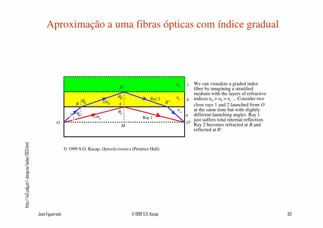
José Figueiredo © 1999 S.O. Kasap 63
nb
nc
O O'Ray 1
A
B'
B
θAθB
θB' Ray 2
M
θB' c/nb
c/na12
B''
na
a
b
c We can visualize a graded indexfiber by imagining a stratifiedmedium with the layers of refractiveindices na > nb > nc ... Consider twoclose rays 1 and 2 launched from Oat the same time but with slightlydifferent launching angles. Ray 1just suffers total internal reflection.Ray 2 becomes refracted at B andreflected at B'.
© 1999 S.O. Kasap, Optoelectronics (Prentice Hall)
Aproximação a uma fibras ópticas com índice gradual
http://w
3.ualg.pt/~jlongras/aulas/OC
S.html
José Figueiredo © 1999 S.O. Kasap 64
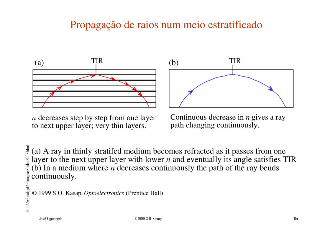
n decreases step by step from one layerto next upper layer; very thin layers.
Continuous decrease in n gives a raypath changing continuously.
TIR TIR
(a) A ray in thinly stratifed medium becomes refracted as it passes from onelayer to the next upper layer with lower n and eventually its angle satisfies TIR.(b) In a medium where n decreases continuously the path of the ray bendscontinuously.
(a) (b)
© 1999 S.O. Kasap, Optoelectronics (Prentice Hall)
Propagação de raios num meio estratificado
http://w
3.ualg.pt/~jlongras/aulas/OC
S.html
José Figueiredo © 1999 S.O. Kasap 65
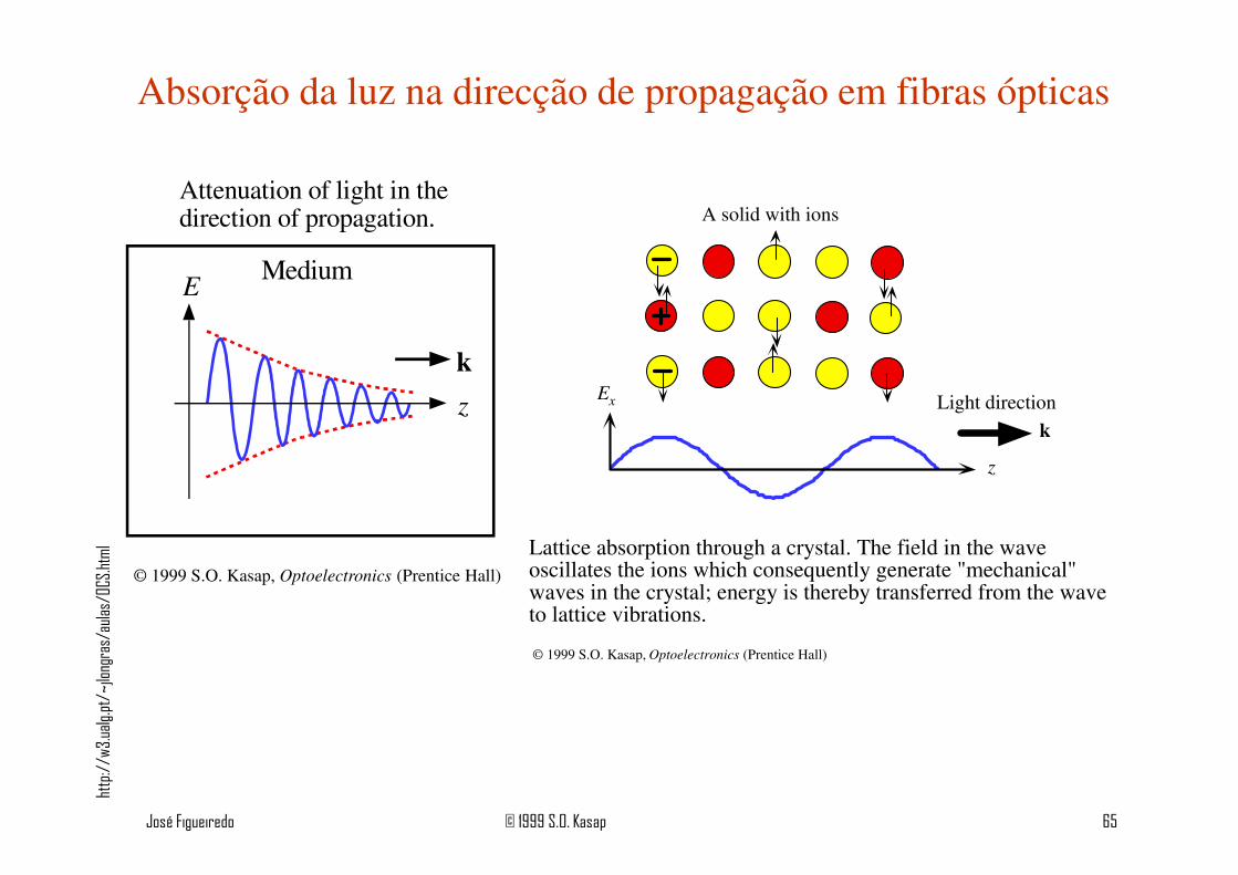
z
A solid with ions
Light direction
k
Ex
Lattice absorption through a crystal. The field in the waveoscillates the ions which consequently generate "mechanical"waves in the crystal; energy is thereby transferred from the waveto lattice vibrations.
© 1999 S.O. Kasap, Optoelectronics (Prentice Hall)
Absorção da luz na direcção de propagação em fibras ópticas
Medium
k
Attenuation of light in thedirection of propagation.
© 1999 S.O. Kasap, Optoelectronics (Prentice Hall)
z
E

http://w
3.ualg.pt/~jlongras/aulas/OC
S.html
José Figueiredo © 1999 S.O. Kasap 66
Scattered waves
Incident wave Through wave
A dielectric particle smaller than wavelength
Rayleigh scattering involves the polarization of a small dielectricparticle or a region that is much smaller than the light wavelength.The field forces dipole oscillations in the particle (by polarizing it)which leads to the emission of EM waves in "many" directions sothat a portion of the light energy is directed away from the incidentbeam.© 1999 S.O. Kasap, Optoelectronics (Prentice Hall)
Espalhamento da luz em fibras ópticas

http://w
3.ualg.pt/~jlongras/aulas/OC
S.html
José Figueiredo © 1999 S.O. Kasap 67
0.05
0.1
0.5
1.0
5
10
0.6 0.8 1.0 1.2 1.4 1.6 1.8 2.0
Latticeabsorption
Rayleighscattering
Wavelength (µm)
Illustration of a typical attenuation vs. wavelength characteristicsof a silica based optical fiber. There are two communicationschannels at 1310 nm and 1550 nm.
OH-absorption peaks
1310 nm
1550 nm
© 1999 S.O. Kasap, Optoelectronics (Prentice Hall)
Atenuação em fibras ópticas de sílica

http://w
3.ualg.pt/~jlongras/aulas/OC
S.html
José Figueiredo © 1999 S.O. Kasap 68
Escaping wave
θ θ
θ′ < θ
θθ > θc θ′
Microbending
R
Cladding
Core
Field distribution
Sharp bends change the local waveguide geometry that can lead to wavesescaping. The zigzagging ray suddenly finds itself with an incidenceangle θ′ that gives rise to either a transmitted wave, or to a greatercladding penetration; the field reaches the outside medium and some lightenergy is lost.
© 1999 S.O. Kasap, Optoelectronics (Prentice Hall)
Perdas em fibras ópticas devido a curvaturas

http://w
3.ualg.pt/~jlongras/aulas/OC
S.html
José Figueiredo © 1999 S.O. Kasap 69
0 2 4 6 8 10 12 14 16 18
Radius of curvature (mm)
10−3
10−2
10−1
1
10
102
αB (m-1) for 10 cm of bend
λ = 633 nmλ = 790 nmV ≈ 2.08
V ≈ 1.67
Measured microbending loss for a 10 cm fiber bent by different amounts of radius ofcurvature R. Single mode fiber with a core diameter of 3.9 µm, cladding radius 48 µm,∆ = 0.004, NA = 0.11, V ≈ 1.67 and 2.08 (Data extracted and replotted with ∆ correctionfrom, A.J. Harris and P.F. Castle, IEEE J. Light Wave Technology, Vol. LT14, pp. 34-40, 1986; see original article for discussion of peaks in αB vs. R at 790 nm).
© 1999 S.O. Kasap, Optoelectronics (Prentice Hall)
Perdas em fibras ópticas devido a micro-curvaturas

http://w
3.ualg.pt/~jlongras/aulas/OC
S.html
José Figueiredo © 1999 S.O. Kasap 70
Preform feed
Furnace 2000°C
Thicknessmonitoring gauge
Take-up drum
Polymer coater
Ultraviolet light or furnacefor curing
Capstan
Schematic illustration of a fiber drawing tower.
© 1999 S.O. Kasap, Optoelectronics (Prentice Hall)
Processo de produção de fibras ópticas

http://w
3.ualg.pt/~jlongras/aulas/OC
S.html
José Figueiredo © 1999 S.O. Kasap 71
Protective polymerinc coating
Buffer tube: d = 1mm
Cladding: d = 125 - 150 µm
Core: d = 8 - 10 µmn
r
The cross section of a typical single-mode fiber with a tight buffertube. (d = diameter)
n1
n2
© 1999 S.O. Kasap, Optoelectronics (Prentice Hall)
Secção transversal de uma fibra óptica mono-modo
http://w
3.ualg.pt/~jlongras/aulas/OC
S.html
José Figueiredo © 1999 S.O. Kasap 72
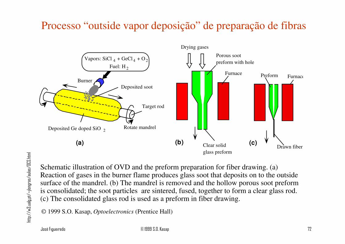
Vapors: SiCl 4 + GeCl 4 + O2
Rotate mandrel
(a)
Deposited sootBurner
Fuel: H 2
Target rod
Deposited Ge doped SiO 2
(b)
Furnace
Porous sootpreform with hole
Clear solidglass preform
Drying gases
(c)
Furnace
Drawn fiber
Preform
Schematic illustration of OVD and the preform preparation for fiber drawing. (a)Reaction of gases in the burner flame produces glass soot that deposits on to the outsidesurface of the mandrel. (b) The mandrel is removed and the hollow porous soot preformis consolidated; the soot particles are sintered, fused, together to form a clear glass rod.(c) The consolidated glass rod is used as a preform in fiber drawing.
© 1999 S.O. Kasap, Optoelectronics (Prentice Hall)
Processo “outside vapor deposição” de preparação de fibras

http://w
3.ualg.pt/~jlongras/aulas/OC
S.html
José Figueiredo © 1999 S.O. Kasap 73
vg (m/s)
ω (1/s)
TE0
TE1
2.08×10⁸
2.07×10⁸
2.06×10⁸
2.05×10⁸
0 1×101 5 2×101 5 3×101 5
ωcut-off = 2.3×101 4
TE4
c/n2
c/n1
Group velocity vs. angular frequency for three modes for a planar dielectric waveguidewhich has n1 = 1.455, n2 = 1.44, a = 10 µm (Results from Mathview, Waterloo Maplemath-software application). TE0 is for m = 0 etc.
© 1999 S.O. Kasap, Optoelectronics (Prentice Hall)
Velocidade de grupo em função da frequência

http://w
3.ualg.pt/~jlongras/aulas/OC
S.html
José Figueiredo © 1999 S.O. Kasap 74
0
0.5
1
1.5
0 1 2 3
V - number
V[d2(Vb)/dV2]
[d2(Vb)/dV2] vs. V-number for a step index fiber (after W.A. Gambling etal., The Radio and Electronics Engineer, 51, 313, 1981)
© 1999 S.O. Kasap, Optoelectronics (Prentice Hall)
Dispersão de perfil

http://w
3.ualg.pt/~jlongras/aulas/OC
S.html
José Figueiredo © 1999 S.O. Kasap 75
n2
n1
O O'
B'
AB
Ray ARay B θ
Aθ
A
θB'
θB'
θB
θB '
y = 0
y = δ/2
δ/2
Medium 1
Medium 2
n3 Medium 3 δ
δ
y = 3δ/2
y = 5δ/2
θB'
θB
B''
Step-graded-index dielectric waveguide. Two rays are launched fromthe center of the waveguide at O at angles θA and θB such that ray Asuffers TIR at A and ray B suffers TIR at B'. Both TIRs are at criticalangles.© 1999 S.O. Kasap, Optoelectronics (Prentice Hall)
Guia de onda dieléctrico com perfil gradual estratificado

http://w
3.ualg.pt/~jlongras/aulas/OC
S.html
José Figueiredo © 1999 S.O. Kasap 76
0.5P
O'O
(a)
0.25P
O
(b)
0.23P
O
(c)
Graded index (GRIN) rod lenses of different pitches. (a) Point O is on the rod facecenter and the lens focuses the rays onto O' on to the center of the opposite face. (b)The rays from O on the rod face center are collimated out. (c) O is slightly away fromthe rod face and the rays are collimated out.
© 1999 S.O. Kasap, Optoelectronics (Prentice Hall)
Lentes com distribuição de índice gradual
José Figueiredo © 1999 S.O. Kasap 77
Optoelectrónica e óptica integrada

http://w
3.ualg.pt/~jlongras/aulas/OC
S.html
José Figueiredo © 1999 S.O. Kasap 78
Wire-grid polarizerE
x
Ey
y
x
z
Ey
The wire grid-acts as a polarizer© 1999 S.O. Kasap, Optoelectronics (Prentice Hall)
Grelha polarizadora

http://w
3.ualg.pt/~jlongras/aulas/OC
S.html
José Figueiredo © 1999 S.O. Kasap 79
x
y
z
Ey
Ex
−yEy
^
xEx
^
(a) (b) (c)
E
Plane of polarization
x̂
y^
E
(a) A linearly polarized wave has its electric field oscillations defined along a lineperpendicular to the direction of propagation, z. The field vector E and z define a plane ofpolarization. (b) The E-field oscillations are contained in the plane of polarization. (c) Alinearly polarized light at any instant can be represented by the superposition of two fields Ex
and Ey with the right magnitude and phase.
E
© 1999 S.O. Kasap, Optoelectronics (Prentice Hall)
Luz linearmente polarizada
http://w
3.ualg.pt/~jlongras/aulas/OC
S.html
José Figueiredo © 1999 S.O. Kasap 80
z
Ey
Ex
EEθ = k∆z
∆z
z
A right circularly polarized light. The field vector E is always at rightangles to z , rotates clockwise around z with time, and traces out a fullcircle over one wavelength of distance propagated.
© 1999 S.O. Kasap, Optoelectronics (Prentice Hall)
Polarização circular direita

http://w
3.ualg.pt/~jlongras/aulas/OC
S.html
José Figueiredo © 1999 S.O. Kasap 81
Estados de polarização
E
y
x
Exo = 0Eyo = 1φ = 0
y
x
Exo = 1Eyo
= 1φ = 0
y
x
Exo = 1Eyo = 1φ = π/2
E
y
x
Exo = 1Eyo = 1φ = −π/2
(a) (b) (c) (d)
Examples of linearly, (a) and (b), and circularly polarized light (c) and (d); (c) isright circularly and (d) is left circularly polarized light (as seen when the wavedirectly approaches a viewer)
E
y
x
Exo = 1Eyo = 2φ = 0
Exo = 1Eyo = 2φ = π/4
Exo = 1Eyo = 2φ = π/2
y
x
(a) (b)E
y
x
(c)
(a) Linearly polarized light with Eyo = 2Exo and φ = 0. (b) When φ = π/4 (45°), the light isright elliptically polarized with a tilted major axis. (c) When φ = π/2 (90°), the light isright elliptically polarized. If Exo and Eyo were equal, this would be right circularlypolarized light.

http://w
3.ualg.pt/~jlongras/aulas/OC
S.html
José Figueiredo © 1999 S.O. Kasap 82
Polarizer 1
TA1
Polarizer 2 = Analyzer
TA2
θ Light detectorE
Ecosθ
Unpolarized light
Linearlypolarized light
Randomly polarized light is incident on a Polarizer 1 with a transmission axis TA1. Lightemerging from Polarizer 1 is linearly polarized with E along TA1, and becomes incidenton Polarizer 2 (called "analyzer") with a transmission axis TA2 at an angle θ to TA1. Adetector measures the intensity of the incident light. TA1 and TA2 are normal to the lightdirection.
© 1999 S.O. Kasap, Optoelectronics (Prentice Hall)
Lei de Malus

http://w
3.ualg.pt/~jlongras/aulas/OC
S.html
José Figueiredo © 1999 S.O. Kasap 83
A line viewed through a cubic sodium chloride (halite) crystal(optically isotropic) and a calcite crystal (optically anisotropic).
Anisotropia óptica – birrefringência

http://w
3.ualg.pt/~jlongras/aulas/OC
S.html
José Figueiredo © 1999 S.O. Kasap 84
Two polaroid analyzers are placed with their transmission axes, alongthe long edges, at right angles to each other. The ordinary ray,undeflected, goes through the left polarizer whereas the extraordinarywave, deflected, goes through the right polarizer. The two wavestherefore have orthogonal polarizations.
Birrefringência e polarização

http://w
3.ualg.pt/~jlongras/aulas/OC
S.html
José Figueiredo © 1999 S.O. Kasap 85
e-wave
o-wave
Optic axis(in plane of paper)
Optic axis
Principal section
e-ray
o-ray
Principal section
A calcite rhomb
E⊥
E/ /Incident ray
Incident wave
An EM wave that is off the optic axis of a calcite crystal splits into two waves calledordinary and extraordinary waves. These waves have orthogonal polarizations andtravel with different velocities. The o-wave has a polarization that is alwaysperpendicular to the optical axis.
© 1999 S.O. Kasap, Optoelectronics (Prentice Hall)
Birrefringência e polarização

http://w
3.ualg.pt/~jlongras/aulas/OC
S.html
José Figueiredo © 1999 S.O. Kasap 86
Optic axis
x , no
y
Ee-wave
Eo-wave
z , ne
Optic axis
y , no
E
z
Ee-wave
Eo-wave
x , no
(a) (b)
(a) A birefringent crystal plate with the optic axis parallel to the plate surfaces. (b) Abirefringent crystal plate with the optic axis perpendicular to the plate surfaces.
© 1999 S.O. Kasap, Optoelectronics (Prentice Hall)
Birrefringência e polarização

http://w
3.ualg.pt/~jlongras/aulas/OC
S.html
José Figueiredo © 1999 S.O. Kasap 87
x = Fast axis
z = Slow axis
E//
E⊥
E//
E⊥
E
L
y
no
ne = n3
α
Optic axis
L
y
no
ne = n3
φ
A retarder plate. The optic axis is parallel to the plate face. The o- and e-waves travelin the same direction but at different speeds.
© 1999 S.O. Kasap, Optoelectronics (Prentice Hall)
Dispositivos baseados na birrefringência – lâminas de atraso

http://w
3.ualg.pt/~jlongras/aulas/OC
S.html
José Figueiredo © 1999 S.O. Kasap 88
Lâminas de atraso
x
α = arbitrary
(b)
Input
z
xE
z
x
(a)
Output
Optic axis
α
α
Half wavelength plate: φ =π Quarter wavelength plate: φ = π/2
x
α
0 < α < 45°
E
z
x
E
E
x
z z
α = 45°
45°
Input and output polarizations of light through (a) a half-wavelengthplate and (b) through a quarter-wavelength plate.
© 1999 S.O. Kasap, Optoelectronics (Prentice Hall)
http://w
3.ualg.pt/~jlongras/aulas/OC
S.html
José Figueiredo © 1999 S.O. Kasap 89
Optic axis
Optic axisd
D
Wedges can slide
Plate
E1
E2
Soleil-Babinet Compensator© 1999 S.O. Kasap, Optoelectronics (Prentice Hall)
Dispositivos de atraso variável
http://w
3.ualg.pt/~jlongras/aulas/OC
S.html
José Figueiredo © 1999 S.O. Kasap 90
Optic axis
e-ray
o-rayA
B
Optic axis
e-ray
o-ray
Optic axis A
B Optic axisθ
E1
E2
E1
E1
E2
E2
The Wollaston prism is a beam polarization splitter. E1 is orthogonal to the plane ofthe paper and also to the optic axis of the first prism. E2 is in the plane of the paperand orthogonal to E1.
© 1999 S.O. Kasap, Optoelectronics (Prentice Hall)
Prismas birrefringentes

http://w
3.ualg.pt/~jlongras/aulas/OC
S.html
José Figueiredo © 1999 S.O. Kasap 91
Outputlight
∆φ
z
x
Ex
d
EyV
z
Ex
Eyy
45°
Inputlight Ea
Tranverse Pockels cell phase modulator. A linearly polarized input light into anelectro-optic crystal emerges as a circularly polarized light. Ea is the applied fieldparallel to y.© 1999 S.O. Kasap, Optoelectronics (Prentice Hall)
Efeitos electro-ópticos
Modulador de fase

http://w
3.ualg.pt/~jlongras/aulas/OC
S.html
José Figueiredo © 1999 S.O. Kasap 92
Transmission intensity
V
Io
Q
0 Vλ/2
V
45°
Inputlight
P A
Detector
Crystal
z
x
y
QWP
Left: A tranverse Pockels cell intensity modulator. The polarizer P and analyzer A havetheir transmission axis at right angles and P polarizes at an angle 45° to y-axis. Right:Transmission intensity vs. applied voltage characteristics. If a quarter-wave plate (QWP)is inserted after P, the characteristic is shifted to the dashed curve.
© 1999 S.O. Kasap, Optoelectronics (Prentice Hall)
Modulador de intensidade

http://w
3.ualg.pt/~jlongras/aulas/OC
S.html
José Figueiredo © 1999 S.O. Kasap 93
V(t)
Ea
Cross-section
LiNbO3
d
Thin buffer layerCoplanar strip electrodes
EO Substratez
y
x
Polarizedinputlight
WaveguideLiNbO 3
L
Integrated tranverse Pockels cell phase modulator in which a waveguide is diffusedinto an electro-optic (EO) substrate. Coplanar strip electrodes apply a transversefield Ea through the waveguide. The substrate is an x-cut LiNbO3 and typically thereis a thin dielectric buffer layer (e.g. ~200 nm thick SiO2) between the surfaceelectrodes and the substrate to separate the electrodes away from the waveguide.
© 1999 S.O. Kasap, Optoelectronics (Prentice Hall)
Modulador ópticos integrados

http://w
3.ualg.pt/~jlongras/aulas/OC
S.html
José Figueiredo © 1999 S.O. Kasap 94
V(t)
LiNbO3 EO Substrate
A
BIn
OutC
DA
B
Waveguide
Electrode
An integrated Mach-Zender optical intensity modulator. The input light issplit into two coherent waves A and B, which are phase shifted by theapplied voltage, and then the two are combined again at the output.
© 1999 S.O. Kasap, Optoelectronics (Prentice Hall)
Modulador Mach-Zehnder

http://w
3.ualg.pt/~jlongras/aulas/OC
S.html
José Figueiredo © 1999 S.O. Kasap 95
Cross-section
Coupled waveguides
B
E
x
EA EB
d
nBnA
Ans
A
B
Top view
Lo
InputPA(Lo)PA(0)
z
PB(Lo)
z
PA(z)
PB(z)(a) (b)
x
(a) Cross section of two closely spaced waveguides A and B (separated by d)embedded in a substrate. The evanescent field from A extends into B and vice versa.Note: nA and nB > ns (= substrate index).(b) Top view of the two guides A and B that are coupled along the z-direction. Lightis fed into A at z = 0, and it is gradually transferred to B along z. At z = Lo, all thelight been transferred to B . Beyond this point, light begins to be transferred back toA in the same way.
© 1999 S.O. Kasap, Optoelectronics (Prentice Hall)
Acoplador direccional passivo
Ver também http://w3.ualg.pt/~jlongras/JLFMScThesis.pdf (4º capítulo)

http://w
3.ualg.pt/~jlongras/aulas/OC
S.html
José Figueiredo © 1999 S.O. Kasap 96
V(t)
LiNbO3
In
Electrode
Waveguides
Fibers
Ea
Cross-section
LiNbO3
V(t)
Coupled waveguides
A B
dA B
Lo
An integrated directional coupler. Applied field Ea alters the refractive indices of thetwo guides and changes the strength of coupling.
© 1999 S.O. Kasap, Optoelectronics (Prentice Hall)
Acoplador direccional activo
http://w
3.ualg.pt/~jlongras/aulas/OC
S.html
José Figueiredo © 1999 S.O. Kasap 97
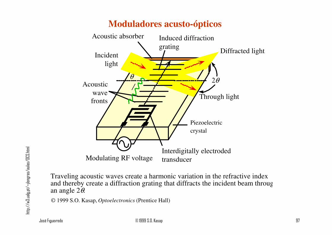
Interdigitally electrodedtransducerModulating RF voltage
Piezoelectriccrystal
Acousticwavefronts
Induced diffractiongrating
Incidentlight
Diffracted light
θ
Through light
Acoustic absorber
2θ
Traveling acoustic waves create a harmonic variation in the refractive indexand thereby create a diffraction grating that diffracts the incident beam throughan angle 2θ.© 1999 S.O. Kasap, Optoelectronics (Prentice Hall)
Moduladores acusto-ópticos

http://w
3.ualg.pt/~jlongras/aulas/OC
S.html
José Figueiredo © 1999 S.O. Kasap 98
θ
A
B
Incident optical beam Diffracted optical beam
O
O'
P Q
B'
A'
Λsinθ Λsinθ
Λ Acousticwave fronts
θ
nmax
nmax
nmin
nmin
nmin n
ma x
x
nmin
nma x
x
nn
Simplified Actual
Acousticwave
vacoustic
Consider two coherent optical waves A and B being "reflected" (strictly,scattered) from two adjacent acoustic wavefronts to become A' and B'. Thesereflected waves can only constitute the diffracted beam if they are in phase. Theangle θ is exaggerated (typically this is a few degrees).
© 1999 S.O. Kasap, Optoelectronics (Prentice Hall)
Moduladores acusto-ópticos
http://w
3.ualg.pt/~jlongras/aulas/OC
S.html
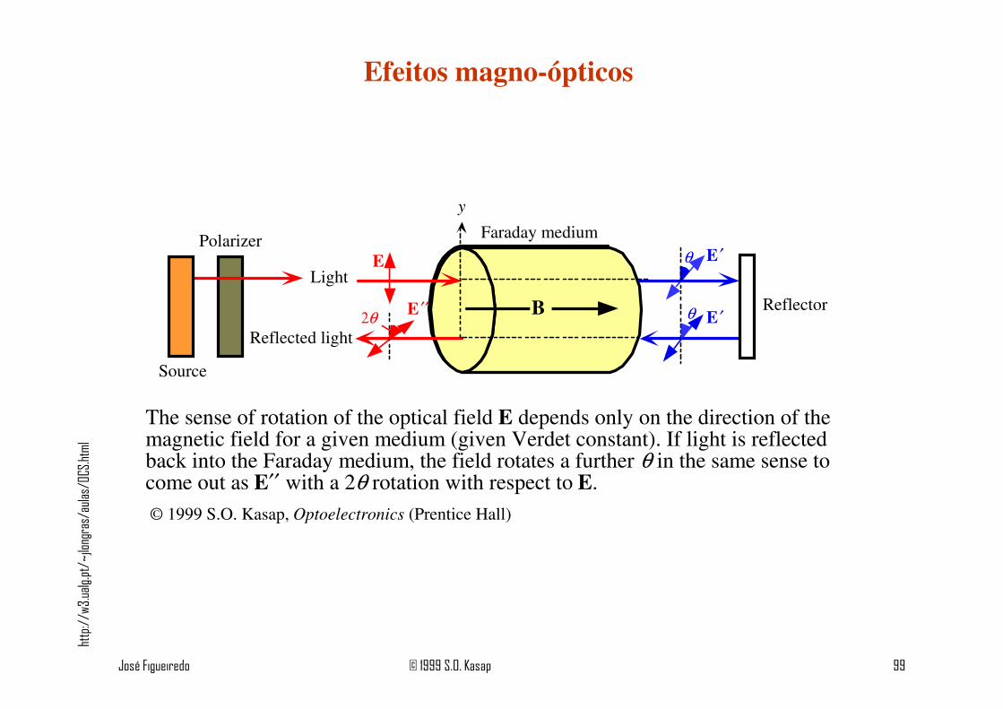
José Figueiredo © 1999 S.O. Kasap 99
E θ E ′
θ E ′2θE ′′
Light
Reflected light
Reflector
Faraday medium
y
Polarizer
Source
The sense of rotation of the optical field E depends only on the direction of themagnetic field for a given medium (given Verdet constant). If light is reflectedback into the Faraday medium, the field rotates a further θ in the same sense tocome out as E′′ with a 2θ rotation with respect to E.
© 1999 S.O. Kasap, Optoelectronics (Prentice Hall)
B
Efeitos magno-ópticos

http://w
3.ualg.pt/~jlongras/aulas/OC
S.html
José Figueiredo © 1999 S.O. Kasap 100
E
P
Eo
−Eo
P+
P-
P
sinωt
-cos2ωt
DC
Eo
−Eo
P+
P-
t
t
t
(a) (b) (c)
(a) Induced polarization vs. optical field for a nonlinear medium. (b) Sinusoidal opticalfield oscillations between ±Eo result in polarization oscillations between P+ and P-. (c)The polarization oscillation can be represented by sinusoidal oscillations at angularfrequencies ω (fundamental), 2ω (second harmonic) and a small DC component.
© 1999 S.O. Kasap, Optoelectronics (Prentice Hall)
Efeitos não-lineares e geração do segundo harmónico

http://w
3.ualg.pt/~jlongras/aulas/OC
S.html
José Figueiredo © 1999 S.O. Kasap 101
S1
Second harmonics
v2
v1
k2
k1
Fundamental
Crystal
S2
S3
As the fundamental wave propagates, it periodically generatessecond harmonic waves (S1, S2, S3, ...) and if these are in phase thenthe amplitude of the second harmonic light builds up.
© 1999 S.O. Kasap, Optoelectronics (Prentice Hall)
Geração do segundo harmónico

http://w
3.ualg.pt/~jlongras/aulas/OC
S.html
José Figueiredo © 1999 S.O. Kasap 102
KDP Optic axisLaser
IMNd:YAGλ = 1064 nm λ = 1064 nm
λ = 532 nm
θλ = 532 nm
Filter
A simplified schematic illustration of optical frequency doubling using a KDP(potassium dihydrogen phosphate) crystal. IM is the index matched direction at anangle θ (about 35°) to the optic axis along which ne(2ω) = no(ω). The focusing ofthe laser beam onto the KDP crystal and the collimation of the light emergingfrom the crystal are not shown.
© 1999 S.O. Kasap, Optoelectronics (Prentice Hall)
Duplicação de frequência
Second harmonicphoton, k2Fundamental photon, k1
Dipole moment-photoninteraction region
Fundamental photon, k1
hω1
hω1
hω2
Photonic interpretation of secondharmonic generation (SHG)
© 1999 S.O. Kasap, Optoelectronics (Prentice Hall)

José Figueiredo 103

http://w
3.ualg.pt/~jlongras/aulas/OC
S.html
José Figueiredo 104
Material semicondutores e sistema MBE
Ver também http://w3.ualg.pt/~jlongras/JLFPhDThesis.pdf (2º capítulo)
© 1998 J Figueiredo
http://w
3.ualg.pt/~jlongras/aulas/OC
S.html
José Figueiredo 105
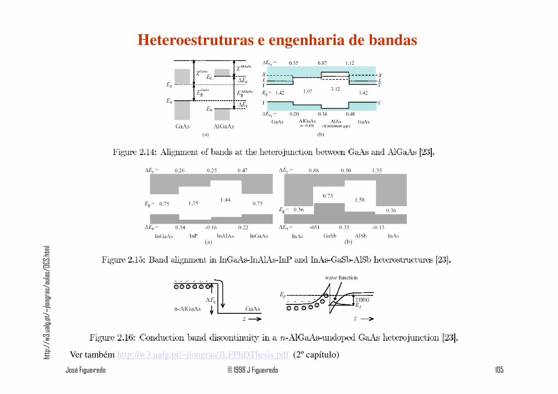
Heteroestruturas e engenharia de bandas
Ver também http://w3.ualg.pt/~jlongras/JLFPhDThesis.pdf (2º capítulo)
© 1998 J Figueiredo
http://w
3.ualg.pt/~jlongras/aulas/OC
S.html
José Figueiredo 106
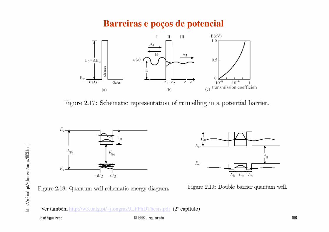
Barreiras e poços de potencial
Ver também http://w3.ualg.pt/~jlongras/JLFPhDThesis.pdf (2º capítulo)
© 1998 J Figueiredo

http://w
3.ualg.pt/~jlongras/aulas/OC
S.html
José Figueiredo 107
Confinamento óptico e confinamento electrónico
Ver também http://w3.ualg.pt/~jlongras/JLFPhDThesis.pdf (2º capítulo)
Guias de onda
© 1998 J Figueiredo

http://w
3.ualg.pt/~jlongras/aulas/OC
S.html
José Figueiredo 108
Perdas em guias de onda
Ver também http://w3.ualg.pt/~jlongras/JLFPhDThesis.pdf (2º capítulo)
© 1998 J Figueiredo

http://w
3.ualg.pt/~jlongras/aulas/OC
S.html
José Figueiredo 109
Electroabsorção em semicondutores
© 1998 J Figueiredo

http://w
3.ualg.pt/~jlongras/aulas/OC
S.html
José Figueiredo 110
Esquemas de modulação
© 1998 J Figueiredo

http://w
3.ualg.pt/~jlongras/aulas/OC
S.html
José Figueiredo 111
Modulação externa por electrorefracção e por electroabsorção
© 1998 J Figueiredo

José Figueiredo 112

http://w
3.ualg.pt/~jlongras/aulas/OC
S.html
José Figueiredo 113
Fabricação de dispositivos ópticos integrados em semincondutores
© 1998 J Figueiredo

http://w
3.ualg.pt/~jlongras/aulas/OC
S.html
José Figueiredo 114
Geração do segundo harmónico
© 1998 J Figueiredo
http://w
3.ualg.pt/~jlongras/aulas/OC
S.html
José Figueiredo © 1998 J Figueiredo 115
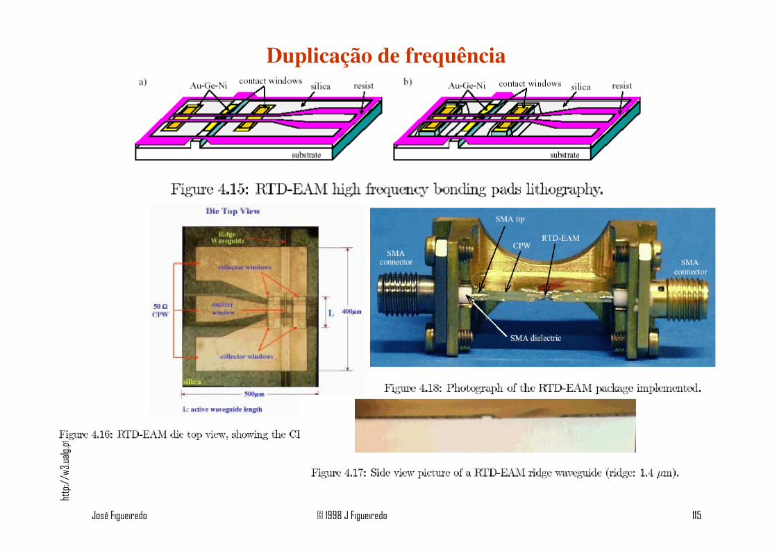
Duplicação de frequência

José Figueiredo © 1999 S.O. Kasap 116

José Figueiredo © 1999 S.O. Kasap 117

José Figueiredo © 1999 S.O. Kasap 118